CN109655944B - Optical element, optical system, and image pickup apparatus - Google Patents
Optical element, optical system, and image pickup apparatus Download PDFInfo
- Publication number
- CN109655944B CN109655944B CN201811190764.6A CN201811190764A CN109655944B CN 109655944 B CN109655944 B CN 109655944B CN 201811190764 A CN201811190764 A CN 201811190764A CN 109655944 B CN109655944 B CN 109655944B
- Authority
- CN
- China
- Prior art keywords
- optical element
- lens
- layer
- refractive index
- element according
- Prior art date
- Legal status (The legal status is an assumption and is not a legal conclusion. Google has not performed a legal analysis and makes no representation as to the accuracy of the status listed.)
- Active
Links
Images


Classifications
-
- G—PHYSICS
- G02—OPTICS
- G02B—OPTICAL ELEMENTS, SYSTEMS OR APPARATUS
- G02B3/00—Simple or compound lenses
-
- G—PHYSICS
- G02—OPTICS
- G02B—OPTICAL ELEMENTS, SYSTEMS OR APPARATUS
- G02B15/00—Optical objectives with means for varying the magnification
- G02B15/14—Optical objectives with means for varying the magnification by axial movement of one or more lenses or groups of lenses relative to the image plane for continuously varying the equivalent focal length of the objective
- G02B15/16—Optical objectives with means for varying the magnification by axial movement of one or more lenses or groups of lenses relative to the image plane for continuously varying the equivalent focal length of the objective with interdependent non-linearly related movements between one lens or lens group, and another lens or lens group
- G02B15/163—Optical objectives with means for varying the magnification by axial movement of one or more lenses or groups of lenses relative to the image plane for continuously varying the equivalent focal length of the objective with interdependent non-linearly related movements between one lens or lens group, and another lens or lens group having a first movable lens or lens group and a second movable lens or lens group, both in front of a fixed lens or lens group
- G02B15/167—Optical objectives with means for varying the magnification by axial movement of one or more lenses or groups of lenses relative to the image plane for continuously varying the equivalent focal length of the objective with interdependent non-linearly related movements between one lens or lens group, and another lens or lens group having a first movable lens or lens group and a second movable lens or lens group, both in front of a fixed lens or lens group having an additional fixed front lens or group of lenses
- G02B15/173—Optical objectives with means for varying the magnification by axial movement of one or more lenses or groups of lenses relative to the image plane for continuously varying the equivalent focal length of the objective with interdependent non-linearly related movements between one lens or lens group, and another lens or lens group having a first movable lens or lens group and a second movable lens or lens group, both in front of a fixed lens or lens group having an additional fixed front lens or group of lenses arranged +-+
-
- G—PHYSICS
- G02—OPTICS
- G02B—OPTICAL ELEMENTS, SYSTEMS OR APPARATUS
- G02B1/00—Optical elements characterised by the material of which they are made; Optical coatings for optical elements
- G02B1/10—Optical coatings produced by application to, or surface treatment of, optical elements
- G02B1/11—Anti-reflection coatings
- G02B1/111—Anti-reflection coatings using layers comprising organic materials
-
- G—PHYSICS
- G02—OPTICS
- G02B—OPTICAL ELEMENTS, SYSTEMS OR APPARATUS
- G02B15/00—Optical objectives with means for varying the magnification
- G02B15/14—Optical objectives with means for varying the magnification by axial movement of one or more lenses or groups of lenses relative to the image plane for continuously varying the equivalent focal length of the objective
- G02B15/144—Optical objectives with means for varying the magnification by axial movement of one or more lenses or groups of lenses relative to the image plane for continuously varying the equivalent focal length of the objective having four groups only
- G02B15/1441—Optical objectives with means for varying the magnification by axial movement of one or more lenses or groups of lenses relative to the image plane for continuously varying the equivalent focal length of the objective having four groups only the first group being positive
- G02B15/144113—Optical objectives with means for varying the magnification by axial movement of one or more lenses or groups of lenses relative to the image plane for continuously varying the equivalent focal length of the objective having four groups only the first group being positive arranged +-++
-
- G—PHYSICS
- G02—OPTICS
- G02B—OPTICAL ELEMENTS, SYSTEMS OR APPARATUS
- G02B27/00—Optical systems or apparatus not provided for by any of the groups G02B1/00 - G02B26/00, G02B30/00
- G02B27/09—Beam shaping, e.g. changing the cross-sectional area, not otherwise provided for
- G02B27/0938—Using specific optical elements
- G02B27/095—Refractive optical elements
- G02B27/0955—Lenses
-
- H—ELECTRICITY
- H04—ELECTRIC COMMUNICATION TECHNIQUE
- H04N—PICTORIAL COMMUNICATION, e.g. TELEVISION
- H04N23/00—Cameras or camera modules comprising electronic image sensors; Control thereof
- H04N23/50—Constructional details
- H04N23/54—Mounting of pick-up tubes, electronic image sensors, deviation or focusing coils
-
- H—ELECTRICITY
- H04—ELECTRIC COMMUNICATION TECHNIQUE
- H04N—PICTORIAL COMMUNICATION, e.g. TELEVISION
- H04N23/00—Cameras or camera modules comprising electronic image sensors; Control thereof
- H04N23/50—Constructional details
- H04N23/55—Optical parts specially adapted for electronic image sensors; Mounting thereof
Landscapes
- Physics & Mathematics (AREA)
- General Physics & Mathematics (AREA)
- Optics & Photonics (AREA)
- Nonlinear Science (AREA)
- Engineering & Computer Science (AREA)
- Multimedia (AREA)
- Signal Processing (AREA)
- Surface Treatment Of Optical Elements (AREA)
- Lenses (AREA)
- Laminated Bodies (AREA)
Abstract
The invention relates to an optical element, an optical system, and an image pickup apparatus. The optical element includes a plurality of substrates, an adhesive bonding the plurality of substrates to each other, and an antireflection film provided to at least one of an incident surface and an exit surface of the optical element. The antireflection film includes a first layer containing an alcohol having a branched structure and having 4 to 7 carbon atoms, the alcohol having at least one of an ether bond and an ester bond. The alcohol content in the first layer was 0.5mg/cm3~5.0mg/cm3. The first layer has a refractive index of 1.1 to 1.3 with respect to light having a wavelength of 550 nm.
Description
Technical Field
The present invention relates to an optical element, an optical system, and an image pickup apparatus (or an image forming apparatus) each having an antireflection film.
Background
A surface of a conventional optical element for an optical system such as a camera lens has an antireflection film for suppressing unnecessary light such as flare (flare) and ghost (ghost) due to reduction in light amount loss and reflection of incident light. Japanese patent laid-open No. (JP) 2012-078597 discloses an antireflection film including a low refractive index layer having a nanoporous silica film.
An optical system such as a camera lens sometimes uses a cemented lens in which a plurality of lenses are attached to each other by an adhesive. JP2012-002888 discloses a method of forming an antireflection film on a cemented lens by using a wet process.
In an attempt to form a wet film on a bonded lens using the method disclosed in JP2012-078597, high-temperature drying and heat treatment after the application of the wet film changes or yellows the bonding adhesive or causes a change in transmittance. Further, the difference in linear expansion coefficient between the glass materials of the two lenses may cause peeling of the adhesive, deformation (distortion) or cracking of the lenses, or the like.
JP2012-002888 discloses shapes of lenses and jigs for preventing a coating liquid from dissolving a binder on a lens joint surface at the time of film formation by a wet process, but there is no description about the composition of the coating liquid and heat treatment after coating.
Disclosure of Invention
The invention provides an optical element having an antireflection film capable of preventing change and peeling of an adhesive and suppressing deterioration of optical performance.
An optical element according to an aspect of the present invention includes a plurality of base materials, an adhesive agent that bonds the plurality of base materials to each other, and a light-emitting element provided to the optical elementAt least one of the light incident surface and the light exit surface of (2). The antireflection film includes a first layer containing an alcohol having a branched structure and having 4 to 7 carbon atoms, the alcohol having at least one of an ether bond and an ester bond. The alcohol content in the first layer was 0.5mg/cm3~5.0mg/cm3. The first layer has a refractive index of 1.1 to 1.3 with respect to light having a wavelength of 550 nm.
Further features of the present invention will become apparent from the following description of exemplary embodiments with reference to the attached drawings.
Drawings
Fig. 1 is a cross-sectional view of a cemented lens as an illustrative optical element according to one embodiment of the present invention.
Fig. 2 is a schematic cross-sectional view of the antireflection film.
Fig. 3 is a schematic view of a low refractive index layer.
Fig. 4 is a schematic diagram of chain-like particles.
Fig. 5 is a sectional view of a cemented lens according to embodiment 1.
Fig. 6 is an electron micrograph of the low refractive index layer according to example 1.
Fig. 7A and 7B are graphs illustrating reflectance characteristics of the anti-reflection film according to example 1.
Fig. 8 is a sectional view of a cemented lens according to embodiment 2.
Fig. 9A and 9B are graphs illustrating reflectance characteristics of the anti-reflection film according to example 2.
Fig. 10 is a sectional view of a cemented lens according to embodiment 3.
Fig. 11A and 11B are graphs illustrating reflectance characteristics of the anti-reflection film according to example 3.
Fig. 12 is a sectional view of an optical system according to embodiment 4.
Fig. 13A and 13B are graphs illustrating reflectance characteristics of the anti-reflection film according to example 4.
Detailed Description
Referring now to the drawings, a description will be given of embodiments of the present invention. In the respective drawings, the same elements will be designated by the same reference numerals, and a repetitive description thereof will be omitted.
Fig. 1 is a cross-sectional view of a cemented lens 10 as an illustrative optical element according to one embodiment of the invention. The cemented lens 10 is an optical element produced by bonding a concave meniscus lens (base material) 11 and a convex meniscus lens (base material) 21 to each other on a bonding surface (or bonding surface) 31 with an adhesive interposed therebetween. The adhesive may be any of acrylic, epoxy and polyene polythiol. This embodiment forms the ordinary antireflection film 12 made of a dielectric thin film layer on the light incident surface 11a, and the antireflection film 22 according to the present invention on the light exit surface 21 b.
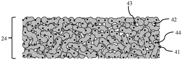
Fig. 2 is a schematic cross-sectional view of the antireflection film 22. In fig. 2, the light exit surface 21b is shown as a flat surface for the sake of simplicity. The antireflection film 22 includes a base layer (or a bottom layer) 23 including a dielectric thin film layer of a single layer or a plurality of layers, and a low refractive index layer (first layer) 24 formed on the base layer 23. This embodiment forms the low refractive index layer 24 on the outermost surface of the antireflection film 22.
The base layer 23 includes a single layer or a plurality of dielectric thin film layers according to the refractive index of the convex meniscus lens 21. In the single layer, the dielectric thin film layer having a refractive index close to the square root of the value obtained by multiplying the refractive index of the convex meniscus lens 21 by the refractive index of the low refractive index layer 24 may be formed so that the optical film thickness (physical film thickness × refractive index) is one quarter of the wavelength at which the reflectance thereof particularly needs to be reduced. In the multilayer, the dielectric thin film layer may be formed by appropriately combining the high refractive index layer and the medium refractive index layer with each other. The high refractive index layer may use zirconium oxide, tantalum oxide, niobium oxide, silicon nitride, silicon oxynitride, titanium oxide, cerium oxide, hafnium oxide, or the like, alone or in combination. As the medium refractive index layer, aluminum oxide, silicon oxynitride, magnesium fluoride, or the like can be used as appropriate. Typically, silicon oxide and magnesium fluoride are often treated as low refractive index layers. Since this embodiment uses the low refractive index layer 24 having a refractive index of 1.1 to 1.3, the medium refractive index layer may also use silicon oxide having a refractive index of about 1.45 and magnesium fluoride having a refractive index of about 1.38.
The base layer 23 is preferably formed by a physical film forming method such as a vacuum deposition method and a sputtering method, but the present invention is not limited to this method. For example, the base layer 23 may be formed by a wet process such as a sol-gel method and a chemical Vapor deposition method such as a cvd (chemical Vapor deposition) method. In the case of using these methods, the base layer 23 needs to be a film that can be formed at a temperature of 80 ℃ or lower, 40 ℃ or lower, or 20 to 25 ℃ so as not to damage the adhesive on the joint surface. The surface of the base layer 23 has a surface hardness of B or more, H or more, or 2H or more in a pencil hardness test defined in JIS K5600.
The low refractive index layer 24 is contained at 0.5mg/cm3~5.0mg/cm3An alcohol having 4 to 7 carbon atoms and a branched structure, having at least one of an ether bond and an ester bond, and having a refractive index of 1.1 to 1.3 with respect to light having a wavelength of 550 nm. The low refractive index layer 24 contains a porous material having a space filling rate of 25% to 85%, and the surface hardness of the surface thereof in a pencil hardness test specified in JIS K5600 is 2B or less. The surface of low refractive index layer 24 may be water-repellent, oil-repellent, or hydrophilic. For example, a fluorine-containing paint, a silicone paint, or the like is applied by vacuum deposition, sputtering, CVD, or the like in a film thickness of about several nm or less that does not give an optical influence.
Referring now to fig. 3, a description will be given of the porous material in low refractive index layer 24. Fig. 3 is a schematic view of low refractive index layer 24. According to this embodiment, the porous material includes secondary particles composed of a plurality of (several to several tens of) particles having as a main component silica particles having an average particle diameter D of 5nm to 40nm, which are connected to each other, and a binder having siloxane bonds. This embodiment uses chain-like particles 41 in which a plurality of fine silica particles having an average particle diameter D of 5nm to 40nm are connected to each other. Instead of the chain-like particles, hollow silica fine particles and magnesium fluoride particles may be used. The use of the secondary particles as chain-like particles made by connecting a plurality of particles in a curved manner can maximize the effect of the present invention and easily manufacture the particles. The average particle size is the average Feret's diameter. The average Ferrett diameter can be measured by processing transmission electron micrographs.
The voids 42 are formed between the chain particles 41 and another chain particle 41, and at least part of the chain particles 41 are linked to each other by the binder 43. The alcohol 44 having an ester bond and a branched structure having 4 to 7 carbon atoms on the surface of the chain particles 41 serves as a spacer between the chain particles 41.
Low refractive index layer 24 contains voids 42 or air having a refractive index of 1.0 and has a refractive index less than that of a film without voids 42. Voids 42 may have a volume fraction of 15% to 75% in low refractive index layer 24. Thus, the chain particles 41, the binder 43, and the alcohol 44 can be prepared at a space filling rate of 25 to 85%. When the space filling rate is 25% or less, the low refractive index layer 24 has an excessively low refractive index of 1.1 or less, good antireflection characteristics cannot be achieved, and a film having significantly low strength and insufficient environmental reliability is produced. When the space filling rate is 85% or more, the refractive index of the low refractive index layer 24 is 1.3 or more and good antireflection characteristics cannot be realized. In order to harmonize the refractive index and the intensity/environmental reliability, the space filling rate can be adjusted to 35% -75% or 45% -65%.
In order to form the low refractive index layer 24 on the surface of the optical element bonded by the adhesive (the light exit surface 21b in this embodiment), the film formation needs to avoid high-temperature heating. This embodiment can obtain a desired porosity by orienting the alcohol 44 in the chain-like particles 41 and form a film without high-temperature heating.
In the following description, "an alcohol having an ether bond or an ester bond, having 4 to 7 carbon atoms, and having a branched structure" will be referred to as "C4-7 branched alcohol". This embodiment applies a dispersion (liquid) containing chain particles 41, a binder 43, and a C4-7 branched alcohol 44 onto the light exit surface 21b, forms a film thickness of 70 to 280nm by allowing the dispersion to stand at room temperature (about 20 to 25 ℃) for about 2 hours, and completes the low refractive index layer 24. When the low refractive index layer placed in a high temperature environment of about 60 ℃ has its characteristics fluctuated only in a practically negligible range, it is determined that the low refractive index layer is "completed". By "practically negligible range" is meant that the thickness and refractive index of the low refractive index film fluctuate within a few percent.
According to this embodiment, the binder 43 has siloxane bonds at the contact portions between the chain particles 41 so as to enhance the film strength, and bonds the chain particles 41 to each other. The binder 43 can be used by mixing a solution containing components necessary for forming the binder 43 composed of a silane alkoxy hydrolysis condensate with a solution in which the chain particles 41 are dispersed in a solvent. Alternatively, a solution in which solid particles connected to each other in a chain-like shape are dispersed in a solvent may be applied, and a solution containing components necessary to form the binder 43 may be applied after aligning the particles.
This embodiment uses a C4-7 branched alcohol 44 as the solvent. Thus, steric hindrance caused by the branched structure of the C4-7 branched alcohol 44 may limit solvent deposition to hydroxyl groups on the particle surface and may be able to maintain a portion of the hydroxyl groups on the particle surface. The C4-7 branched alcohol 44 becomes a spacer and serves to widen the voids 42 between the chain-like particles 41. As shown in fig. 4, the chain particles 41 have a structure in which a plurality of silica particles are bent and connected to each other. The presence of the C4-7 branched alcohol 44 near the contact points between the silica fine particles can provide the effect of widening the voids 42.
The chain length of the C4-7 branched alcohol 44 used as a spacer may be longer in order to lower the refractive index or increase the volume fraction of voids 42 in low refractive index layer 24. However, as the chain length becomes longer, the boiling point of the solvent rises and high temperature heating is required to evaporate the solvent that does not coordinate to the particles. On the other hand, as the chain length becomes too short, the volume ratio of the voids 42 decreases and the refractive index increases. In forming a film by a wet process such as a spin coating method, partial drying starts before a coating film is spread on the surface of an optical element, and the film cannot be uniformly formed. Thus, alcohols having a branched structure of 4 to 7 carbon atoms or 5 to 6 carbon atoms may be favored.
The effect of widening the voids 42 depends on the structure of the ether bond or ester bond. The alcohol having at least one of an ether bond and an ester bond causes an enhanced spacer effect due to a hydrogen bond between an unshared electron pair of an ether bond or oxygen contained in an ester bond and a hydroxyl group on the surface of the particle. This constitution can form a low refractive index film having small scattering in visible light.
The C4-7 branched alcohol 44 includes at least one of 1-propoxy-2-propanol, 1-ethoxy-2-propanol, 2-isopropoxyethanol, 3-methoxy-1-butanol, 1-methoxy-2-propanol, 1-butoxy-2-propanol, methyl lactate, and ethyl lactate.
Low refractive index layer 24 may comprise 0.5mg/cm3~5.0mg/cm3Or 1.0mg/cm3~2.8mg/cm3(inclusive) C4-7 branched alcohol 44. When the amount of C4-7 branched alcohol 44 is less than 0.5mg/cm3When this occurs, the low refractive index layer 24 contracts and the refractive index becomes higher. On the other hand, when the amount of C4-7 branched alcohol 44 is greater than 5.0mg/cm3When the refractive index is lowered by the solvent itself.
As described above, the present invention can form a low refractive index layer having a refractive index of 1.1 to 1.3 (inclusive) for light having a wavelength of 550nm without heating at a high temperature. Since the low refractive index layer 24 according to this embodiment is formed by leaving it in an environment of about 20 to 25 ℃ for about 2 hours, it can be applied not only to a bonded lens but also to a bonded prism, a plastic lens, a film, and the like. In order to form low refractive index layer 24 in a short time, the layer may be heated in an unaffected range on the surface of the optical element.
In order to restrict the adhesive peeling and the lens deformation or crack, a cemented lens manufactured by attaching the first lens and the second lens to each other may satisfy a condition where α1(×10-7K-1) Is the linear expansion coefficient, alpha, of the material of the first lens2(×10-7K-1) Is the linear expansion coefficient of the material of the second lens, and phic(mm) is an outer diameter of a junction surface between the first lens and the second lens.
2.0×10²≤φc×|α1-α2|≤2.0×10⁴ (1)
The following conditions may be satisfied.
5.0×10²≤φc×|α1-α2|≤1.0×10⁴ (2)
Example 1
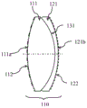
Fig. 5 is a sectional view of the cemented lens 110 according to this embodiment. The cemented lens 110 is an optical element produced by bonding the double convex lens 111 and the concave meniscus lens 121 to each other on the cemented surface 131 with an adhesive interposed therebetween. The lenticular lens 111 consists of a refractive index n for the d-line (wavelength 587.56nm)dS-FPL51, OHARA Corp. of 1.497. The concave meniscus lens 121 consists of a refractive index n to d-linedS-LAH65V, OHARA Corp. 1.804. The outer diameter of the engagement surface 131 is 30.0 mm. This embodiment forms the ordinary antireflection film 112 composed of a dielectric multilayer film on the light incident surface 111a of the cemented lens 110, and the antireflection film 122 according to the present invention on the light exit surface 121b of the cemented lens 110. Table 1 shows the design values of the antireflection film 122.
A description will now be given of an illustrative manufacturing method of the cemented lens 110. First, the optical surfaces (light incident surface and light exit surface) of the lenticular lens 111 and the concave meniscus lens 121 are polished, and the outer peripheral portion (generally referred to as edge) of the lens is centered (center).
Next, the antireflection film 112 is formed on the light incident surface 111a of the lenticular lens 111. It is not necessary to provide the dielectric thin film layer on the light exit surface (the same surface as the bonding surface 131) of the lenticular lens 111. This is because the refractive index of the lenticular lens 111 is close to that of the adhesive for bonding and the reflectance at the interface is sufficiently small.
Next, after an aluminum oxide layer (refractive index of 1.65) was formed on the light incident surface (the same surface as the bonding surface 131) of the concave meniscus lens 121 with a thickness of 83.5nm, the underlayer in the anti-reflection film 122 according to the present invention was formed on the light exit surface 121b by a vacuum deposition method. According to this embodiment, the base layer is a dielectric thin film layer including 8 alternating layers of alumina and zirconia as shown in table 1. Although this embodiment forms the base layer by a vacuum evaporation method, the present invention is not limited to this example, and a sputtering method or a wet method may be used. In addition, as for the membrane material, alumina and zirconia are used in this embodiment, but the present invention is not limited to this example.
Next, the double convex lens 111 and the concave meniscus lens 121 are bonded to each other by an adhesive (a polyene polythiol-based adhesive OP-1045K manufactured by DENKA co. More specifically, when the light exit surface 121b of the concave meniscus lens 121 is directed downward, the adhesive is dropped on the bonding surface 131, the double convex lens 111 is aligned with and pressed against a proper position, and then UV light is irradiated and the adhesive is cured. The thickness of the adhesive may be 1 to 100 μm or 3 to 20 μm. This embodiment sets the thickness of the adhesive to about 7 μm. The cured adhesive according to this embodiment has a refractive index of 1.52. Although this embodiment uses the polyene polythiol-based adhesive DENKA co., ltd. OP-1045K as the adhesive, the present invention is not limited to this example.
Although the adhesive can be dropped by a necessary amount calculated from the thickness and the area and spread completely uniformly on the bonding surface 131, the control is substantially difficult. It is therefore necessary to drop a larger amount of adhesive than necessary and remove the excess adhesive protruding from the outer peripheral portion (edge) of the bonding surface 131. The usual removal method is wiping off with a nonwoven or paper cloth (handkerchief) impregnated with an organic solvent before or after curing. When a porous soft film (having a surface hardness of 2B or less in pencil hardness) is formed on the outermost surface of the anti-reflection film 122, wiping contact or solvent adhesion causes fluctuation in reflectance characteristics or causes scratches and contamination. In this embodiment, the outermost surface of the antireflection film 122 in the bonding step is the outermost surface of the base layer. Therefore, the outermost surface of the base layer has a surface hardness of B or more, H or more, or 2H or more in pencil hardness. According to this embodiment, the outermost surface of the base layer is a zirconia layer having a pencil hardness of 2H or more, and never causes scratches or a poor appearance due to wiping or washing.
After the bonding step is completed, a low refractive index layer is formed on the base layer. A description will now be given of a dispersion liquid containing chain-like particles for the low refractive index layer according to this embodiment.
This example used an IPA dispersion of chain-like particles (IPA-ST-UP (registered trademark); solid content 15 wt%) manufactured by Nissan Chemical Industries, Co., Ltd.) to prepare a dispersion. A 1-propoxy-2-propanol dispersion (solid content concentration 17 wt%) of chain-like particles was prepared by replacing the 2-propanol solvent in the IPA dispersion with 1-propoxy-2-propanol (manufactured by Sigma) using an evaporator. The catalyst ratio was 2-propanol to 1-propoxy-2-propanol-7.5: 92.5.
The binder solution was prepared by: 18.5g of tetraethoxysilane (also referred to as TEOS or ethyl silicate, manufactured by Tokyo Chemical Industry Co., Ltd.) and 16.0g of 0.1 wt% phosphinic acid corresponding to ten equivalents of TEOS were added as catalyst water, and the mixed solution was stirred at 20 ℃ for 60 minutes. 32.8g of a binder solution (equivalent to 0.5 wt% in terms of oxides) was added to the slurry, wherein the binder solution was mixed with 251.3g of a 1-propoxy-2-propanol dispersion of chain particles to form a binder. Thereafter, 174.5g of 1-propoxy-2-propanol and 546.5g of ethyl lactate were added to adjust the solid content (when converted into an oxide) of the chain particles to 4.3 wt%, and the mixture was stirred for 60 minutes, thereby obtaining 1-propoxy-2-propanol and ethyl lactate of 40: 60.
Next, the bonding lens 110 was mounted in a spin coater with its light emitting surface 121b facing upward, and 0.2ml of the dispersion was dropped to spin at 4000rpm for 20 seconds. Thereafter, the product was left at room temperature of 23 ℃ for 2 hours under a clean room atmosphere, and the bonded lens 110 was completed.
Linear expansion coefficient α of glass material of the lenticular lens 1111Is 131 [. times.10 ]-7K-1]Linear expansion coefficient α of glass material of concave meniscus lens 1212Is 60 [. times.10 ]-7K-1]. When the cemented lens 110 has a large difference in linear expansion coefficient, forming the low refractive index layer without heat treatment can prevent peeling of the adhesive, prevent cracking of the lens, or prevent deterioration of the lens surface accuracy due to stress, providing good antireflection performance.
The present inventors have empirically recognized that when the linear expansion coefficient difference is 30 [. times.10 [ ]-7K-1]In the above, problems such as peeling and cracks are caused by the treatment at 80 ℃. Difference in linear expansion coefficient of60[×10-7K-1]The above causes problems such as deterioration of surface accuracy at a temperature of about 40 ℃. Of course, although the degree of the problem depends on the shape such as the outer diameter and thickness of the lens, the brittleness of the glass material, and the like, the above values are rough estimates.
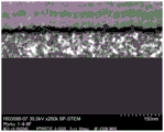
A description will now be given of the evaluation results of the optical element having the antireflection film formed on the silicon substrate. The low refractive index layer is formed on the outermost surface of the antireflection film using a dispersion liquid. Fig. 6 shows a scanning transmission electron microscope photograph of the low refractive index layer. In fig. 6, the treatment for protecting the structure from electron beam irradiation makes the surface of the low refractive index layer black. Voids (white portions in fig. 6) are formed between the curved and connected chain-like particles. The refractive index of the low refractive index layer was 1.238 according to evaluation of the low refractive index layer with a spectroscopic ellipsometer (j.a. woollam Co.).
Silica or silica typically has a refractive index of about 1.45. Since the particles and the binder are also substantially made of silicon oxide, the space filling rate of the low refractive index layer is about 55.1%. The surface hardness of the low refractive index layer is 2B or less.
The amount of solvent residue and binder in the low refractive index layer were measured by using a column such as Thermo Scientific headspace (header) TRIPLUS300, mass spectrum LSQ LT, gas chromatography RAC GC ULTRA, Frontier Laboratories ULTRA Alloy Series (model: UA + -5), and the like. According to the measurement conditions, the heating temperature of the oven in the headspace was 160 ℃, the equilibration time was 30 minutes, the purge time was 3 minutes, the temperature of the ion source in the mass spectrum was 220 ℃, and the heating temperature of the injection port in the gas chromatograph was 200 ℃. The oven heating conditions were as follows: the initial temperature was held at 40 ℃ for 1 minute, the temperature was increased to 200 ℃ at a rate of 5.0 ℃/min, the temperature was held at 200 ℃ for 10 minutes, the temperature was increased to 320 ℃ at a rate of 20.0 ℃/min, and the temperature was held at 320 ℃ for 5 minutes.
The base plate prepared in a 10ml sample tube was set as an internal standard, and sealed with a chloroform solution to which 0.15 wt% of naphthalene was added and measured. Every 1cm3Based on the film thickness on the optical element on which the antireflection film is formedAnd the area of the silicon substrate.
In calculating the solvent residual amount, a calibration curve of the solvent was made by adding 0.13 wt%, 0.23 wt%, 0.35 wt%, and 0.62 wt% of the solvent to be detected to a chloroform solution to which 0.15 wt% of naphthalene was added.
In calculating the binder amount, a calibration curve of pentamers of the ethyl silicate hydrolysis condensate was prepared by adding pentamers of 0.06 wt%, 0.15 wt%, 0.27 wt%, and 0.40 wt% of the ethyl silicate hydrolysis condensate to a chloroform solution to which 0.15 wt% of naphthalene was added. Peak areas from tetramer to octamer of the ethyl silicate hydrolysis condensate obtained by GC-MS were summarized, and the binder amount of pentamer as the ethyl silicate hydrolysis condensate was evaluated. Ethyl silicate 40 (manufactured by Colcoat co., ltd.) was used as a pentamer of the ethyl silicate hydrolysis condensate.
The evaluation result showed that the residual amount of the solvent in the low refractive index layer was 2.4mg/cm3The amount of binder was 0.5 wt%.
The content (solvent residue) of the dispersion in the low refractive index layer was 0.5mg/cm3~5.0mg/cm3And an alcohol having at least one of an ether bond and an ester bond, having 4 to 7 carbon atoms, and having a branched structure. The composition can provide a low refractive index layer having a refractive index of 1.1 to 1.3 (inclusive) for light having a wavelength of 550nm without high-temperature treatment. Wherein a low refractive index layer having a refractive index of 1.20 to 1.26 with respect to light having a wavelength of 550nm, which harmonizes high antireflection performance and environmental reliability, can be prepared by3~2.8mg/cm3To form the dispersion of (a).
Fig. 7A and 7B show spectral reflectance characteristics of the anti-reflection film 122, in which the horizontal axis represents wavelength and the vertical axis represents reflectance. In fig. 7A, the range of the vertical axis is 5%. In fig. 7B, the range of the vertical axis is 1%. As shown in fig. 7A and 7B, the antireflection film 122 has such high antireflection performance of a wavelength of 430 to 670nm that is substantially sensitive to an image pickup element generally used for a digital camera, such as a CCD and a CMOS. More specifically, the anti-reflection film 122 has a high anti-reflection performance of about 0.1% or less for light rays having an incident angle of 0 ° to 30 °, and a high anti-reflection performance of about 0.5% or less for light rays having an incident angle of 45 °. Therefore, an optical system including the cemented lens 110, for example, a camera lens, has high quality in which unnecessary light such as flare and ghost can be suppressed.
TABLE 1

Example 2
Fig. 8 is a cross-sectional view of the cemented lens 210 according to this embodiment. The cemented lens 210 is an optical element produced by bonding a double convex lens 211 and a double concave lens 212 to each other on a bonding surface 231 via an adhesive. The lenticular lens 211 consists of a refractive index n to d-linedTAFD 30 of HOYA corp. 1.883. The bi-concave lens 212 consists of a refractive index n to d-lined1.596 OHARA Corp. S-TIM 8. The outer diameter of the engagement surface 231 is 42.8 mm. This embodiment forms the ordinary antireflection film 212 composed of a dielectric multilayer film on the light incident surface 211a of the cemented lens 210, and the antireflection film 222 according to the present invention on the light exit surface 221b of the cemented lens 210. Table 2 shows the design values of the antireflection film 222. The antireflection film 222 includes a base layer formed by a vacuum deposition method, and a low refractive index layer formed on the base layer. In this embodiment, the base layer is a dielectric thin film layer comprising 6 alternating layers of alumina and zirconia as shown in table 2.
The cemented lens 210 is manufactured by substantially the same method as that of the cemented lens 110 according to embodiment 1. A description will now be given of the difference of the manufacturing method of the cemented lens 210 according to this embodiment from the cemented lens 110 according to embodiment 1.
This example used a polyene polythiol-based adhesive, OP-1055H manufactured by DENKA co. The lenticular lens 211 and the biconcave lens 212 were attached to each other such that the thickness of the adhesive was 10 μm, UV light was irradiated thereto, and then an excessive amount of the adhesive was wiped off. Thereafter, an inner surface antireflection coating (light-shielding coating) GT-7II by Canon Chemicals co.
The low refractive index layer in the antireflection film 222 according to this embodiment is formed in substantially the same manner as in embodiment 1, except that the proportion of the solvent and the like is appropriately adjusted. Linear expansion coefficient α of glass material of the lenticular lens 2111Is 66 [. times.10 ]-7K-1]And the linear expansion coefficient alpha of the glass material of the biconcave lens 2122Is 84 [. times.10 ]-7K-1]。18[×10-7K-1]Is used to cure the antireflective interior surface coating GT-7II applied to the edge, a low refractive index layer is formed and dried by convection oven at a temperature of 80 ℃ for 20 minutes. According to the analysis of the low refractive index layer according to this example formed on the silicon substrate, the residual amount of the solvent in the low refractive index layer was 1.2mg/cm3The amount of binder was 0.7 wt%.
Fig. 9A and 9B illustrate spectral reflectance characteristics of the antireflection film 222. The antireflection film 222 has a high antireflection function for a wavelength of 430nm to 670 nm. More specifically, it has a high anti-reflection property of about 0.1% or less for light rays having an incident angle of 0 ° to 30 °, and a high anti-reflection property of about 0.5% or less for light rays having an incident angle of 45 °. Therefore, an optical system including the cemented lens 210, for example, a camera lens, has high quality in which unnecessary light such as flare and ghost can be suppressed.
TABLE 2

Example 3
Fig. 10 is a sectional view of the cemented lens 310 according to this embodiment. The joint lens 310 is an optical element produced by bonding the concave meniscus lens 311 and the convex meniscus lens 312 to each other on the joint surface 331 with an adhesive interposed therebetween. The concave meniscus lens 311 consists of a refractive index n to d-linedS-LAH60 of OHARA Corp. 1.834. The convex meniscus 312 is formed by a refractive index n to d-linedS-FPL53, OHARA Corp. 1.439. The outer diameter of the engaging surface 331 is84.0 mm. This embodiment forms a general antireflection film 312 made of a dielectric multilayer film on the light incident surface 311a of the cemented lens 310, and an antireflection film 322 according to the present invention on the light exit surface 321b of the cemented lens 310. Table 3 shows the design values of the antireflection film 322. The antireflection film 322 includes a base layer formed by a vacuum deposition method, and a low refractive index layer formed on the base layer. In this embodiment, the base layer is a dielectric thin film layer comprising 4 alternating layers of alumina and zirconia as shown in table 3.
The cemented lens 310 is manufactured by substantially the same method as that of the cemented lenses according to embodiments 1 and 2. A description will now be given of the difference in the manufacturing method of the cemented lens 310 according to this embodiment from those of the cemented lenses according to embodiments 1 and 2.
This example uses cemede co.ltd. two-component adhesive 1565 as the adhesive. The concave meniscus lens 311 and the convex meniscus lens 312 were attached to each other such that the thickness of the adhesive was 10 μm. Then, excess adhesive was wiped off, and the adhesive was left at room temperature of 23 ℃ for 24 hours and cured. Next, GT-7II of an inner surface antireflection coating (light-shielding coating) Canon Chemicals co.
The low refractive index layer in the antireflection film 322 according to this embodiment is formed in substantially the same manner as in embodiment 1. Linear expansion coefficient α of glass material of concave meniscus lens 3111Is 56 [. times.10 ]-7K-1]And the linear expansion coefficient alpha of the glass material of the convex meniscus lens 3122Is 145 [. times.10 ]-7K-1]. Since 89 [. times.10 [)-7K-1]The large difference in linear expansion coefficient of the cemented lens 310 and the large outer diameter of the cemented surface 331 of 84.0mm are highly likely to cause peeling of the adhesive and deterioration of the lens surface accuracy even at a temperature of about 40 ℃. However, the low refractive index layer according to the present invention can be cured at room temperature of 23 ℃, and problems such as peeling and deterioration of surface precision do not occur.
Fig. 11A and 11B show spectral reflectance characteristics of the antireflection film 322. The antireflection film 322 has a high antireflection function for a wavelength of 430nm to 670 nm. More specifically, it has a high anti-reflection property of about 0.1% or less for light rays having an incident angle of 0 ° to 30 °, and a high anti-reflection property of about 0.5% or less for light rays having an incident angle of 45 °. Therefore, an optical system including the joint lens 310, for example, a camera lens has high quality in which unnecessary light such as flare and ghost can be suppressed.
TABLE 3

Example 4
Fig. 12 is a sectional view of the optical system 101 according to this embodiment. The optical system 101 according to this embodiment is provided in an image pickup apparatus. The image pickup apparatus includes an image pickup element 103, such as a CCD and a CMOS, which receives an image formed by the optical system 101. The optical system 101 may be held by a lens barrel (holder), not shown, and the lens barrel may be detachably attached to the image pickup apparatus.
The optical system 101 is a zoom lens, and includes, in order from the object side, a first lens unit L1 having positive refractive power (positive reactive power), a second lens unit L2 having negative refractive power (negative reactive power), a third lens unit L3 having positive refractive power, and a fourth lens unit L4 having positive refractive power. The optical system 101 includes an aperture stop 102.
In zooming from the wide-angle end to the telephoto end, the second lens unit L2 and the third lens unit L3 move on the optical axis so as to widen the distance between the first lens unit L1 and the second lens unit L2 and narrow the distance between the second lens unit L2 and the third lens unit L3.
The first lens unit L1 includes a 1 a-th lens unit L1a including a single lens having a positive refractive power from the object side, and a 1 b-th lens unit L1b having a full positive refractive power. Upon focusing from an infinity object to a close (or short distance) object, the 1 b-th lens unit 1b moves to the object side on the optical axis.
Numerical embodiment 1 shows design values according to this embodiment and a lens surface distance or interval at the time of zooming, where (a) shows design values of the optical system 101, R is a radius of curvature of the lens, D is a surface distance (lens center thickness), n is a refractive index to D-line, and ν is an abbe number.
In the optical system 101 according to this embodiment, the second lens unit L2 moves significantly upon zooming, and optical design for limiting flare and ghost at all positions is difficult. In particular, in the seventh lens image side indicated by a dotted line, the radius of curvature is infinite (or flat), and the light reflected on the surface of the image pickup element 103 is reflected again and is likely to reach the image plane, causing ghost. Thus, this embodiment forms the antireflection film 422 according to the present invention on the imaging side of the seventh lens.
The seventh lens is bonded to the sixth lens with an adhesive, and a cemented lens 410 is formed. The sixth lens consists of a refractive index n to d-linedS-BSL7 of OHARA Corp. at 1.516. The seventh lens has a refractive index n to d-linedS-TIH53W of OHARA Corp. 1.847. The outer diameter of the engaging surface engaging the lens 410 is 28.4 mm.
This example used a polythiol-based binder OP-1055H, DENKA co, ltd, for the binder as in example 2. The sixth lens and the seventh concave lens were attached to each other such that the thickness of the adhesive was 5 μm, UV light was irradiated thereto, and then excess adhesive was wiped off. Next, GT-7II of an inner surface antireflection coating (light-shielding coating) Canon Chemicals co. This embodiment forms a general antireflection film made of a dielectric thin film layer on the light incident surface of the cemented lens 410, and an antireflection film 422 according to the present invention on the light exit surface of the cemented lens 410. Table 4 shows the design values of the antireflection film 422. The antireflection film 422 includes a base layer (underlayer) formed by a vacuum deposition method, and a low refractive index layer formed on the base layer. In this embodiment, the base layer is a dielectric thin film layer comprising 8 alternating layers of alumina and zirconia as shown in table 4.
The low refractive index layer in the antireflection film 422 according to this embodiment is formed in substantially the same manner as in embodiment 1, except that the proportion of the solvent and the like is appropriately adjusted. Linear expansion coefficient alpha of glass material of sixth lens1Is 72 [. times.10 ]-7K-1]And the linear expansion coefficient alpha of the glass material of the seventh lens2Is 88 [. times.10 ]-7K-1]。16[×10- 7K-1]Is used to cure the antireflective interior surface coating GT-7II applied to the edge, a low refractive index layer is formed and dried by convection oven at a temperature of 40 ℃ for 60 minutes. According to the analysis of the low refractive index layer according to this example formed on the silicon substrate, the residual amount of the solvent in the low refractive index layer was 1.8mg/cm3The amount of binder was 0.6 wt%.
Fig. 13A and 13B illustrate spectral reflectance characteristics of the antireflection film 422. The antireflection film 422 has a high antireflection function for a wavelength of 430nm to 670 nm. More specifically, it has a high anti-reflection property of about 0.08% or less for light rays having an incident angle of 0 ° to 30 °, and a high anti-reflection property of about 0.5% or less for light rays having an incident angle of 45 °. Therefore, even when the lens that may cause ghost moves upon zooming, it can suppress unnecessary light such as flare and ghost, and the optical system 101 also has high quality.
TABLE 4

Numerical example 1
(a)

Radius of curvature (R) and surface distance (D) are in mm.
The refractive index (N) is the value for the d-line at a wavelength of 587.56 nm.
And nu is the Abbe number.
(b)

Unit: mm is
Table 5 shows the numerical values of the cemented lenses according to examples 1 to 4.
TABLE 5


Examples 1-4 discuss illustrative cemented lenses made by fitting two lenses to each other, but the present invention is not limited to these examples. The present invention is also applicable to a cemented lens produced by bonding three or more lenses to each other. The cemented lens according to embodiments 1 to 4 has the antireflection film according to the present invention formed on the light exit surface, but it may be formed on the light entrance surface. The optical system according to embodiment 4 has one cemented lens according to the present invention, but may include a plurality of cemented lenses according to the present invention.
While the present invention has been described with reference to exemplary embodiments, it is to be understood that the invention is not limited to the disclosed exemplary embodiments. The scope of the following claims is to be accorded the broadest interpretation so as to encompass all such modifications and equivalent structures and functions.
Claims (15)
1. An optical element, comprising:
a plurality of substrates;
an adhesive for bonding the plurality of base materials to each other; and
an antireflection film provided to at least one of a light incident surface and a light exit surface of the optical element,
characterized in that the antireflection film comprises a first layer containing an alcohol having 4 to 7 carbon atoms and a branched structure, the alcohol having at least one of an ether bond and an ester bond,
wherein the alcohol content in the first layer is 0.5mg/cm3~5.0mg/cm3,
Wherein the first layer has a refractive index of 1.1 to 1.3 with respect to light having a wavelength of 550nm, and
wherein the first layer is made of a porous material with a space filling rate of 25-85%.
2. The optical element of claim 1, wherein the anti-reflective film comprises a substrate layer on which the first layer is disposed.
3. An optical element as recited in claim 2, wherein said base layer comprises a dielectric thin film layer.
4. The optical element of claim 1, wherein the porous material comprises at least one of silicon oxide and magnesium fluoride.
5. The optical element according to claim 1, wherein the porous material comprises secondary particles and a binder having a siloxane bond, and the secondary particles are formed by interconnecting a plurality of particles having an average particle diameter of 5nm to 40nm and containing silica particles as a main component.
6. The optical element according to claim 1, wherein the alcohol comprises at least one of 1-propoxy-2-propanol, 1-ethoxy-2-propanol, 2-isopropoxyethanol, 3-methoxy-1-butanol, 1-methoxy-2-propanol, 1-butoxy-2-propanol, methyl lactate and ethyl lactate.
7. The optical element of claim 1, wherein the alcohol comprises 1-propoxy-2-propanol and ethyl lactate.
8. The optical element according to claim 1, wherein the alcohol content in the first layer is 1.0mg/cm3~2.8mg/cm3。
9. The optical element according to claim 2, wherein the surface of the base layer has a surface hardness of B or more in a pencil hardness test specified in JIS K5600.
10. The optical element according to claim 1, wherein the adhesive is made of any one of acrylic, epoxy and polyene polythiol.
11. The optical element according to claim 2, wherein the base layer comprises two or more of zirconium oxide, tantalum oxide, niobium oxide, silicon nitride, silicon oxynitride, titanium oxide, cerium oxide, hafnium oxide, aluminum oxide, silicon oxide, and magnesium fluoride.
12. An optical element according to claim 1, wherein the optical element includes a first lens and a second lens bonded to each other via the adhesive, and the following condition is satisfied:
2.0×10²≤φc×|α1-α2|≤2.0×10⁴
wherein alpha is1Is the linear expansion coefficient, alpha, of the material of the first lens2Is the linear expansion coefficient of the material of the second lens, phicIs the outer diameter of the junction surface between the first lens and the second lens, where α1And alpha2Has a unit of x 10- 7K-1,φcIn mm.
13. Optical element according to claim 12, characterized in that the following condition is fulfilled:
5.0×10²≤φc×|α1-α2|≤1.0×10⁴。
14. an optical system, comprising:
an optical element according to any one of claims 1 to 13; and
a holder configured to hold the optical element.
15. An image pickup apparatus characterized by comprising:
an optical system comprising the optical element according to any one of claims 1 to 13; and
an image pickup element configured to receive an image formed by the optical system.
Applications Claiming Priority (2)
| Application Number | Priority Date | Filing Date | Title |
|---|---|---|---|
| JP2017198157A JP7118615B2 (en) | 2017-10-12 | 2017-10-12 | Optical element, optical system and imaging device |
| JP2017-198157 | 2017-10-12 |
Publications (2)
| Publication Number | Publication Date |
|---|---|
| CN109655944A CN109655944A (en) | 2019-04-19 |
| CN109655944B true CN109655944B (en) | 2021-09-07 |
Family
ID=66096249
Family Applications (1)
| Application Number | Title | Priority Date | Filing Date |
|---|---|---|---|
| CN201811190764.6A Active CN109655944B (en) | 2017-10-12 | 2018-10-12 | Optical element, optical system, and image pickup apparatus |
Country Status (3)
| Country | Link |
|---|---|
| US (1) | US11553120B2 (en) |
| JP (1) | JP7118615B2 (en) |
| CN (1) | CN109655944B (en) |
Families Citing this family (17)
| Publication number | Priority date | Publication date | Assignee | Title |
|---|---|---|---|---|
| US20170031525A1 (en) | 2010-05-14 | 2017-02-02 | Racing Optics, Inc. | Touch screen shield |
| US9295297B2 (en) | 2014-06-17 | 2016-03-29 | Racing Optics, Inc. | Adhesive mountable stack of removable layers |
| US10459123B2 (en) * | 2017-03-10 | 2019-10-29 | Canon Kabushiki Kaisha | Optical member, image pickup apparatus, and method for manufacturing optical member |
| JP6850200B2 (en) * | 2017-05-31 | 2021-03-31 | 富士フイルム株式会社 | Endoscopes and endoscope devices |
| US11585962B2 (en) * | 2018-10-19 | 2023-02-21 | Racing Optics, Inc. | Transparent covering having anti-reflective coatings |
| US11846788B2 (en) | 2019-02-01 | 2023-12-19 | Racing Optics, Inc. | Thermoform windshield stack with integrated formable mold |
| US11364715B2 (en) | 2019-05-21 | 2022-06-21 | Racing Optics, Inc. | Polymer safety glazing for vehicles |
| US11648723B2 (en) | 2019-12-03 | 2023-05-16 | Racing Optics, Inc. | Method and apparatus for reducing non-normal incidence distortion in glazing films |
| JP7499018B2 (en) * | 2019-12-03 | 2024-06-13 | Hoya株式会社 | Near-infrared cut filter and imaging device equipped with same |
| US11548356B2 (en) | 2020-03-10 | 2023-01-10 | Racing Optics, Inc. | Protective barrier for safety glazing |
| JP7575256B2 (en) * | 2020-12-04 | 2024-10-29 | 株式会社タムロン | Cemented lens, optical system including same, optical device, and method for manufacturing cemented lens |
| JP7604208B2 (en) * | 2020-12-11 | 2024-12-23 | キヤノン株式会社 | Optical element and optical device including same |
| US11490667B1 (en) | 2021-06-08 | 2022-11-08 | Racing Optics, Inc. | Low haze UV blocking removable lens stack |
| US12140781B2 (en) | 2021-07-27 | 2024-11-12 | Laminated Film Llc | Low reflectance removable lens stack |
| US11709296B2 (en) | 2021-07-27 | 2023-07-25 | Racing Optics, Inc. | Low reflectance removable lens stack |
| CN114217451B (en) * | 2021-12-10 | 2023-06-13 | 中国科学院光电技术研究所 | lens system |
| US11808952B1 (en) | 2022-09-26 | 2023-11-07 | Racing Optics, Inc. | Low static optical removable lens stack |
Citations (5)
| Publication number | Priority date | Publication date | Assignee | Title |
|---|---|---|---|---|
| CN1776460A (en) * | 2004-11-18 | 2006-05-24 | 株式会社日立制作所 | Anti-reflection diaphragm and manufacturing, display device, optical storage medium and solar energy conversion device |
| JP2010217699A (en) * | 2009-03-18 | 2010-09-30 | Konica Minolta Opto Inc | Composition for antireflective layer, antireflective film, polarizing plate and image display apparatus |
| CN102186668A (en) * | 2008-10-17 | 2011-09-14 | 日立化成工业株式会社 | Film having low refractive index and method for producing the same, anti-reflection film and method for producing the same, coating liquid set for film having low refractive index, substrate having microparticle-laminated thin film, and method for pr |
| JP2012002888A (en) * | 2010-06-15 | 2012-01-05 | Nikon Corp | Optical member |
| CN102472842A (en) * | 2009-08-04 | 2012-05-23 | 大日本印刷株式会社 | Optical laminate, polarizing plate, and image display device |
Family Cites Families (22)
| Publication number | Priority date | Publication date | Assignee | Title |
|---|---|---|---|---|
| JP2935769B2 (en) | 1992-04-02 | 1999-08-16 | 富士写真光機株式会社 | Manufacturing method of antireflection film |
| JPH07104102A (en) | 1993-09-30 | 1995-04-21 | Olympus Optical Co Ltd | Water repellant reflection preventive film for glass-made optical parts and production thereof |
| JP3497236B2 (en) | 1994-04-28 | 2004-02-16 | オリンパス株式会社 | Anti-reflection coating for high precision optical components |
| JPH0836101A (en) | 1994-07-22 | 1996-02-06 | Victor Co Of Japan Ltd | Antireflection film of optical parts made of synthetic resin |
| JPH08136703A (en) | 1994-11-08 | 1996-05-31 | Olympus Optical Co Ltd | Film formation of antireflection film |
| JPH08201601A (en) | 1995-01-24 | 1996-08-09 | Olympus Optical Co Ltd | Production of antireflection film |
| JPH1171458A (en) | 1996-08-14 | 1999-03-16 | Asahi Optical Co Ltd | Transparent resin and composite with adhesiveness, ultraviolet-curable composition for coating film formation, anti-reflection glass with scattering prevention function, cushioning material, ultraviolet-cutting sheet, ultraviolet-cutting filter for television, filter for vdt, and high-refractive-index primer composition and production of lens with primer using the primer composition |
| JP4836316B2 (en) * | 1999-09-29 | 2011-12-14 | 富士フイルム株式会社 | Antireflection film, polarizing plate, and image display device |
| JP2003140037A (en) * | 2001-11-01 | 2003-05-14 | Pentax Corp | Cemented lens |
| JP2004191741A (en) * | 2002-12-12 | 2004-07-08 | Asahi Kasei Corp | Coating composition for antireflection film |
| JP2005300576A (en) | 2004-04-06 | 2005-10-27 | Konica Minolta Opto Inc | Glare-proof antireflection film, polarizing plate and display device |
| JP2009008901A (en) * | 2007-06-28 | 2009-01-15 | Nikon Corp | Antireflection film, optical element and optical system |
| KR100995401B1 (en) * | 2008-04-30 | 2010-11-19 | 주식회사 엘지화학 | Hollow magnesium fluoride particles, preparation method thereof and anti-reflective coating solution comprising the same |
| JP5403411B2 (en) | 2009-06-17 | 2014-01-29 | 株式会社ニコン | Converter lens and optical apparatus having the same |
| JP5614214B2 (en) | 2010-10-01 | 2014-10-29 | リコーイメージング株式会社 | Antireflection film and optical member having antireflection film |
| JP5340252B2 (en) * | 2010-11-17 | 2013-11-13 | キヤノン株式会社 | Antireflection film and method for manufacturing the same |
| CN103608705B (en) * | 2011-06-06 | 2016-10-12 | 旭硝子株式会社 | Optical filter, solid-state imager, imaging device lens and camera head |
| JP2015108642A (en) * | 2012-03-12 | 2015-06-11 | 富士フイルム株式会社 | Cemented lens |
| JP6360660B2 (en) * | 2013-05-23 | 2018-07-18 | 日揮触媒化成株式会社 | Base material with antireflection film and method for producing the same |
| JP6532228B2 (en) * | 2014-12-10 | 2019-06-19 | キヤノン株式会社 | Optical member and method of manufacturing optical member |
| KR102524754B1 (en) * | 2015-09-09 | 2023-04-21 | 엘지디스플레이 주식회사 | Display device |
| JP2017167271A (en) * | 2016-03-15 | 2017-09-21 | キヤノン株式会社 | Optical member and manufacturing method for optical member |
-
2017
- 2017-10-12 JP JP2017198157A patent/JP7118615B2/en active Active
-
2018
- 2018-10-10 US US16/156,259 patent/US11553120B2/en active Active
- 2018-10-12 CN CN201811190764.6A patent/CN109655944B/en active Active
Patent Citations (5)
| Publication number | Priority date | Publication date | Assignee | Title |
|---|---|---|---|---|
| CN1776460A (en) * | 2004-11-18 | 2006-05-24 | 株式会社日立制作所 | Anti-reflection diaphragm and manufacturing, display device, optical storage medium and solar energy conversion device |
| CN102186668A (en) * | 2008-10-17 | 2011-09-14 | 日立化成工业株式会社 | Film having low refractive index and method for producing the same, anti-reflection film and method for producing the same, coating liquid set for film having low refractive index, substrate having microparticle-laminated thin film, and method for pr |
| JP2010217699A (en) * | 2009-03-18 | 2010-09-30 | Konica Minolta Opto Inc | Composition for antireflective layer, antireflective film, polarizing plate and image display apparatus |
| CN102472842A (en) * | 2009-08-04 | 2012-05-23 | 大日本印刷株式会社 | Optical laminate, polarizing plate, and image display device |
| JP2012002888A (en) * | 2010-06-15 | 2012-01-05 | Nikon Corp | Optical member |
Also Published As
| Publication number | Publication date |
|---|---|
| JP7118615B2 (en) | 2022-08-16 |
| CN109655944A (en) | 2019-04-19 |
| US20190116300A1 (en) | 2019-04-18 |
| JP2019074547A (en) | 2019-05-16 |
| US11553120B2 (en) | 2023-01-10 |
Similar Documents
| Publication | Publication Date | Title |
|---|---|---|
| CN109655944B (en) | Optical element, optical system, and image pickup apparatus | |
| JP4858170B2 (en) | Method for producing MgF2 optical thin film having amorphous silicon oxide binder | |
| JP7301508B2 (en) | Cemented lens, optical system having the same, optical equipment, and cemented lens manufacturing method | |
| TWI432770B (en) | Optical system | |
| JP2019074547A5 (en) | ||
| JP6903994B2 (en) | Optical element and its manufacturing method | |
| CN111263910A (en) | lens unit | |
| WO2018062298A1 (en) | Lens unit and imaging device | |
| JP2018141822A (en) | Optical element, manufacturing method thereof, and optical device | |
| EP3223042B1 (en) | Optical member and method of manufacturing the same | |
| JP2023073340A (en) | Lens unit and camera module | |
| JP2013033124A (en) | Optical element, and optical system and optical equipment using the same | |
| US7626772B2 (en) | Optical system and optical apparatus having the same | |
| JP2017049313A (en) | Antireflection film, optical member, method of manufacturing antireflection film and method of manufacturing optical member | |
| KR20180103763A (en) | Optical member, image pickup apparatus, and method for manufacturing optical member | |
| CN108572404B (en) | Optical member, imaging apparatus, and method of manufacturing optical member | |
| JP7401351B2 (en) | Components, optical equipment, coating fluids, manufacturing methods for components, porous membranes | |
| EP4266089A1 (en) | Article including porous layer containing inorganic particles, and coating liquid for forming porous layer containing inorganic particles | |
| JP2020181073A (en) | Lens with film, lens unit, and camera module | |
| CN204331079U (en) | Antifogging self-cleaning optical mirror | |
| JP7563019B2 (en) | Coverslips | |
| US20220187502A1 (en) | Optical element and optical device including the same | |
| Bae et al. | Endoscope camera using tunable liquid-filled lens with antireflective structures | |
| JP2021096392A (en) | Optical element with antireflection film | |
| JP2019159174A (en) | Film-coated lens, lens unit, and camera module |
Legal Events
| Date | Code | Title | Description |
|---|---|---|---|
| PB01 | Publication | ||
| PB01 | Publication | ||
| SE01 | Entry into force of request for substantive examination | ||
| SE01 | Entry into force of request for substantive examination | ||
| GR01 | Patent grant | ||
| GR01 | Patent grant |