CN108780114B - Method and system for temperature control of devices in an electronic tester - Google Patents
Method and system for temperature control of devices in an electronic tester Download PDFInfo
- Publication number
- CN108780114B CN108780114B CN201780011541.6A CN201780011541A CN108780114B CN 108780114 B CN108780114 B CN 108780114B CN 201780011541 A CN201780011541 A CN 201780011541A CN 108780114 B CN108780114 B CN 108780114B
- Authority
- CN
- China
- Prior art keywords
- temperature
- wafer
- assembly
- slot
- frame
- Prior art date
- Legal status (The legal status is an assumption and is not a legal conclusion. Google has not performed a legal analysis and makes no representation as to the accuracy of the status listed.)
- Active
Links
Images


Classifications
-
- H—ELECTRICITY
- H01—ELECTRIC ELEMENTS
- H01L—SEMICONDUCTOR DEVICES NOT COVERED BY CLASS H10
- H01L22/00—Testing or measuring during manufacture or treatment; Reliability measurements, i.e. testing of parts without further processing to modify the parts as such; Structural arrangements therefor
- H01L22/30—Structural arrangements specially adapted for testing or measuring during manufacture or treatment, or specially adapted for reliability measurements
-
- G—PHYSICS
- G01—MEASURING; TESTING
- G01R—MEASURING ELECTRIC VARIABLES; MEASURING MAGNETIC VARIABLES
- G01R31/00—Arrangements for testing electric properties; Arrangements for locating electric faults; Arrangements for electrical testing characterised by what is being tested not provided for elsewhere
- G01R31/003—Environmental or reliability tests
-
- G—PHYSICS
- G01—MEASURING; TESTING
- G01R—MEASURING ELECTRIC VARIABLES; MEASURING MAGNETIC VARIABLES
- G01R31/00—Arrangements for testing electric properties; Arrangements for locating electric faults; Arrangements for electrical testing characterised by what is being tested not provided for elsewhere
- G01R31/28—Testing of electronic circuits, e.g. by signal tracer
- G01R31/282—Testing of electronic circuits specially adapted for particular applications not provided for elsewhere
- G01R31/2831—Testing of materials or semi-finished products, e.g. semiconductor wafers or substrates
-
- G—PHYSICS
- G01—MEASURING; TESTING
- G01R—MEASURING ELECTRIC VARIABLES; MEASURING MAGNETIC VARIABLES
- G01R31/00—Arrangements for testing electric properties; Arrangements for locating electric faults; Arrangements for electrical testing characterised by what is being tested not provided for elsewhere
- G01R31/28—Testing of electronic circuits, e.g. by signal tracer
- G01R31/2851—Testing of integrated circuits [IC]
- G01R31/2855—Environmental, reliability or burn-in testing
- G01R31/2872—Environmental, reliability or burn-in testing related to electrical or environmental aspects, e.g. temperature, humidity, vibration, nuclear radiation
- G01R31/2874—Environmental, reliability or burn-in testing related to electrical or environmental aspects, e.g. temperature, humidity, vibration, nuclear radiation related to temperature
- G01R31/2875—Environmental, reliability or burn-in testing related to electrical or environmental aspects, e.g. temperature, humidity, vibration, nuclear radiation related to temperature related to heating
-
- G—PHYSICS
- G01—MEASURING; TESTING
- G01R—MEASURING ELECTRIC VARIABLES; MEASURING MAGNETIC VARIABLES
- G01R31/00—Arrangements for testing electric properties; Arrangements for locating electric faults; Arrangements for electrical testing characterised by what is being tested not provided for elsewhere
- G01R31/50—Testing of electric apparatus, lines, cables or components for short-circuits, continuity, leakage current or incorrect line connections
-
- H—ELECTRICITY
- H01—ELECTRIC ELEMENTS
- H01L—SEMICONDUCTOR DEVICES NOT COVERED BY CLASS H10
- H01L21/00—Processes or apparatus adapted for the manufacture or treatment of semiconductor or solid state devices or of parts thereof
- H01L21/02—Manufacture or treatment of semiconductor devices or of parts thereof
- H01L21/04—Manufacture or treatment of semiconductor devices or of parts thereof the devices having at least one potential-jump barrier or surface barrier, e.g. PN junction, depletion layer or carrier concentration layer
- H01L21/18—Manufacture or treatment of semiconductor devices or of parts thereof the devices having at least one potential-jump barrier or surface barrier, e.g. PN junction, depletion layer or carrier concentration layer the devices having semiconductor bodies comprising elements of Group IV of the Periodic System or AIIIBV compounds with or without impurities, e.g. doping materials
- H01L21/30—Treatment of semiconductor bodies using processes or apparatus not provided for in groups H01L21/20 - H01L21/26
- H01L21/324—Thermal treatment for modifying the properties of semiconductor bodies, e.g. annealing, sintering
-
- H—ELECTRICITY
- H01—ELECTRIC ELEMENTS
- H01L—SEMICONDUCTOR DEVICES NOT COVERED BY CLASS H10
- H01L21/00—Processes or apparatus adapted for the manufacture or treatment of semiconductor or solid state devices or of parts thereof
- H01L21/67—Apparatus specially adapted for handling semiconductor or electric solid state devices during manufacture or treatment thereof; Apparatus specially adapted for handling wafers during manufacture or treatment of semiconductor or electric solid state devices or components ; Apparatus not specifically provided for elsewhere
- H01L21/67005—Apparatus not specifically provided for elsewhere
- H01L21/67011—Apparatus for manufacture or treatment
- H01L21/67098—Apparatus for thermal treatment
- H01L21/67103—Apparatus for thermal treatment mainly by conduction
-
- H—ELECTRICITY
- H01—ELECTRIC ELEMENTS
- H01L—SEMICONDUCTOR DEVICES NOT COVERED BY CLASS H10
- H01L21/00—Processes or apparatus adapted for the manufacture or treatment of semiconductor or solid state devices or of parts thereof
- H01L21/67—Apparatus specially adapted for handling semiconductor or electric solid state devices during manufacture or treatment thereof; Apparatus specially adapted for handling wafers during manufacture or treatment of semiconductor or electric solid state devices or components ; Apparatus not specifically provided for elsewhere
- H01L21/67005—Apparatus not specifically provided for elsewhere
- H01L21/67011—Apparatus for manufacture or treatment
- H01L21/67098—Apparatus for thermal treatment
- H01L21/67109—Apparatus for thermal treatment mainly by convection
-
- H—ELECTRICITY
- H01—ELECTRIC ELEMENTS
- H01L—SEMICONDUCTOR DEVICES NOT COVERED BY CLASS H10
- H01L21/00—Processes or apparatus adapted for the manufacture or treatment of semiconductor or solid state devices or of parts thereof
- H01L21/67—Apparatus specially adapted for handling semiconductor or electric solid state devices during manufacture or treatment thereof; Apparatus specially adapted for handling wafers during manufacture or treatment of semiconductor or electric solid state devices or components ; Apparatus not specifically provided for elsewhere
- H01L21/67005—Apparatus not specifically provided for elsewhere
- H01L21/67242—Apparatus for monitoring, sorting or marking
- H01L21/67248—Temperature monitoring
-
- H—ELECTRICITY
- H01—ELECTRIC ELEMENTS
- H01L—SEMICONDUCTOR DEVICES NOT COVERED BY CLASS H10
- H01L21/00—Processes or apparatus adapted for the manufacture or treatment of semiconductor or solid state devices or of parts thereof
- H01L21/67—Apparatus specially adapted for handling semiconductor or electric solid state devices during manufacture or treatment thereof; Apparatus specially adapted for handling wafers during manufacture or treatment of semiconductor or electric solid state devices or components ; Apparatus not specifically provided for elsewhere
- H01L21/683—Apparatus specially adapted for handling semiconductor or electric solid state devices during manufacture or treatment thereof; Apparatus specially adapted for handling wafers during manufacture or treatment of semiconductor or electric solid state devices or components ; Apparatus not specifically provided for elsewhere for supporting or gripping
- H01L21/687—Apparatus specially adapted for handling semiconductor or electric solid state devices during manufacture or treatment thereof; Apparatus specially adapted for handling wafers during manufacture or treatment of semiconductor or electric solid state devices or components ; Apparatus not specifically provided for elsewhere for supporting or gripping using mechanical means, e.g. chucks, clamps or pinches
- H01L21/68714—Apparatus specially adapted for handling semiconductor or electric solid state devices during manufacture or treatment thereof; Apparatus specially adapted for handling wafers during manufacture or treatment of semiconductor or electric solid state devices or components ; Apparatus not specifically provided for elsewhere for supporting or gripping using mechanical means, e.g. chucks, clamps or pinches the wafers being placed on a susceptor, stage or support
- H01L21/68785—Apparatus specially adapted for handling semiconductor or electric solid state devices during manufacture or treatment thereof; Apparatus specially adapted for handling wafers during manufacture or treatment of semiconductor or electric solid state devices or components ; Apparatus not specifically provided for elsewhere for supporting or gripping using mechanical means, e.g. chucks, clamps or pinches the wafers being placed on a susceptor, stage or support characterised by the mechanical construction of the susceptor, stage or support
-
- H—ELECTRICITY
- H01—ELECTRIC ELEMENTS
- H01L—SEMICONDUCTOR DEVICES NOT COVERED BY CLASS H10
- H01L22/00—Testing or measuring during manufacture or treatment; Reliability measurements, i.e. testing of parts without further processing to modify the parts as such; Structural arrangements therefor
- H01L22/20—Sequence of activities consisting of a plurality of measurements, corrections, marking or sorting steps
- H01L22/26—Acting in response to an ongoing measurement without interruption of processing, e.g. endpoint detection, in-situ thickness measurement
-
- G—PHYSICS
- G01—MEASURING; TESTING
- G01R—MEASURING ELECTRIC VARIABLES; MEASURING MAGNETIC VARIABLES
- G01R1/00—Details of instruments or arrangements of the types included in groups G01R5/00 - G01R13/00 and G01R31/00
- G01R1/02—General constructional details
- G01R1/04—Housings; Supporting members; Arrangements of terminals
- G01R1/0408—Test fixtures or contact fields; Connectors or connecting adaptors; Test clips; Test sockets
- G01R1/0491—Test fixtures or contact fields; Connectors or connecting adaptors; Test clips; Test sockets for testing integrated circuits on wafers, e.g. wafer-level test cartridge
Abstract
The invention provides a tester device. The trough assembly is removably mounted to the frame. Each slot assembly allows for individual heating and temperature control of a respective cartridge inserted into the slot assembly. A closed loop air passage is defined by the frame, and a heater and a cooler are located in the closed loop air passage to cool or heat the cartridge with air. Individual cartridges may be inserted or removed while other cartridges are in various stages of testing or in various stages of temperature ramping.
Description
Technical Field
The invention relates to a test device for testing microelectronic circuits.
Background
Microelectronic circuits are commonly fabricated in and on semiconductor wafers. Such wafers are then "singulated" or "diced" into individual dies. Such dies are typically mounted on a supporting substrate to provide rigidity thereto and are in electronic communication with a collection of dies or microelectronic circuitry. The final assembly may include packaging of the die, and the resulting assembly may then be shipped to a customer.
Requiring testing of the die or assembly prior to shipment to the customer. Ideally, the die should be tested at an early stage to identify defects that occurred during the early manufacturing process. Wafer level testing may be accomplished by providing a handler having contacts and a contactor, and then using the handler to move the wafer to bring the contacts on the wafer into contact with the contacts on the contactor. Power and electrical signals may then be provided through the contacts to the microelectronic circuits formed in the wafer.
According to various embodiments, a wafer includes a substrate, such as a silicon substrate or a printed circuit board, and one or more devices fabricated in or mounted to the substrate.
Alternatively, the wafer may be located in a portable cassette having an electrical interface and a thermal chuck. Power and signals may be provided to and from the wafer through the electrical interface while the temperature of the wafer is thermally controlled by heating or cooling the thermal chuck.
Disclosure of Invention
The present invention provides a tester apparatus comprising a frame, a plurality of slot assemblies, each slot assembly comprising a slot assembly body mounted on the frame, a holder mounted on the slot assembly body and forming a test station for placing a respective wafer, the respective wafer having at least one microelectronic device, a plurality of electrical conductors and a temperature detector proximate the respective wafer to detect a temperature of the respective wafer, at least one temperature regulating device that when operated causes heat to be transferred to or from the wafer, at least one thermal controller that controls heat transfer based on the temperature of the wafer detected by the temperature detector, a power supply connected to the wafer in the test station through the electrical conductors and providing at least electrical power to each microelectronic device, and a tester connected to the wafer through the electrical conductors and measuring a performance of the microelectronic device.
The present invention also provides a method of testing a microelectronic device, comprising: placing a respective wafer of a plurality of wafers, each wafer having at least one microelectronic device, in a respective test station provided by a respective holder of a respective slot assembly mounted on a frame, detecting a respective temperature of the respective wafer with a respective temperature detector proximate the respective wafer, transferring heat to or from the wafer, controlling heat transfer based on the temperature of the wafer detected by the temperature detector, testing the microelectronic devices by providing at least power to each microelectronic device and measuring a performance of the microelectronic device.
The present invention also provides a tester apparatus comprising: a frame defining at least a first closed loop air passage; at least a first fan located in the first closed loop air passage to recirculate air through the first closed loop air passage; a plurality of slot assemblies, each slot assembly comprising: a tank assembly body mounted on the frame; a holder mounted on the tank assembly body and forming a test station for placement of a respective wafer having at least one microelectronic device and held in the first closed loop air channel; and a plurality of electrical conductors; a temperature regulating device mounted on the frame in the first closed loop air passage, the temperature regulating device, when in operation, causing heat transfer between air in the first closed loop air passage and the temperature regulating device in the first closed loop air passage; at least one temperature detector for detecting temperature; a thermal controller to control heat transfer based on the temperature; a power supply connected to the wafer in the test station by the electrical conductors and providing at least electrical power to each microelectronic device; and a tester connected to the wafer through the electrical conductors and measuring a performance of the microelectronic device.
The invention also provides a method of testing a microelectronic device, comprising: placing a respective wafer of a plurality of wafers, each having at least one microelectronic device, in a respective test station provided by a respective holder of a respective slot assembly mounted on a frame, the wafer being held in a first closed loop air channel defined by the frame; operating at least a first fan located in the first closed loop air passage to recirculate air through the first closed loop air passage; transferring heat between at least one temperature regulating device mounted on the frame in the first closed loop air passage and air in the first closed loop air passage; detecting the temperature; controlling heat transfer based on the temperature; and testing the microelectronic devices by providing at least power to each microelectronic device and measuring the performance of the microelectronic device.
The present invention also provides a tester apparatus comprising: a frame; a plurality of slot assemblies, each slot assembly comprising: a tank assembly body mounted on the frame; a holder mounted on the pod assembly body and forming a test station for placing a respective wafer, the respective wafer having at least one microelectronic device; a plurality of electrical conductors; and a temperature detector proximate to the respective wafer to detect a temperature of the respective wafer; at least one temperature regulating device that when operated causes heat to be transferred to or from the wafer; and a tester connected to the wafers in the test station by the electrical conductors to test each microelectronic device by providing at least power to the microelectronic device and measuring a performance of the microelectronic device, wherein at least one conductor of a first slot assembly is connectable between a first wafer and the power supply while transferring heat to or from a second wafer connected to the power supply.
The present invention also provides a method of testing a microelectronic device, comprising: placing a respective wafer of a plurality of wafers, each having at least one microelectronic device, in a respective test station provided by a respective holder of a respective slot assembly mounted on a frame; detecting a respective temperature of the respective wafer with a respective temperature detector proximate to the respective wafer; transferring heat to or from the wafer; testing each microelectronic device by providing at least power to the microelectronic device and measuring a performance of the microelectronic device; and connecting at least one conductor of the first tank assembly between the first wafer and the power source while transferring heat to or from a second wafer connected to the power source.
Drawings
The invention is further described by way of example with reference to the accompanying drawings, in which:
FIG. 1 is a cross-sectional side view of a tester device having a slot assembly according to one embodiment of the invention;
FIG. 2 is a cross-sectional side view of the tester device shown in FIG. 1 taken along section line 2-2;
FIG. 3 is a cross-sectional side view of the tester device shown in FIG. 1, taken along section line 3-3;
FIG. 4 is a cross-sectional side view of the tester device shown in FIGS. 2 and 3, taken along section line 4-4;
FIG. 5A is a cross-sectional side view of a tester device having a slot assembly according to another embodiment of the invention;
FIGS. 5B and 5C are cross-sectional side views of a tester device having a slot assembly according to yet another embodiment of the invention;
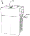
6A, 6B, and 6C are perspective views of the tester apparatus showing insertion or removal of a portable case into or out of an oven defined by a frame;
FIG. 7 is a timing diagram showing how one cassette is inserted and used to test the electronics of a wafer, and then another cassette is inserted; and
FIG. 8 is a perspective view of the tester device showing the insertion or removal of one slot assembly.
Detailed Description
FIG. 1 of the drawings shows a tester apparatus 10 according to one embodiment of the invention, which includes a tester 12, a frame 14, a power bus 16, first and second slot assemblies 18A and 18B, first and second tester interfaces 20A and 20B, first and second power interfaces 22A and 22B, first and second pressurized air interfaces 24A and 24B, first and second vacuum interfaces 26A and 26B, first and second cassettes 28A and 28B, and first and second wafers 30A and 30B.
The tank assembly 18A includes a tank assembly body 32, a thermal chuck 34, a temperature detector 36, a temperature regulating device in the form of a heating element 38, a cooling element 39, a first tank assembly interface 40, and a plurality of second tank assembly interfaces including a control interface 44, a power supply interface 46, and a vacuum interface 48.
The first tank assembly interface 40 is located within the tank assembly body 32 and is mounted to the tank assembly body 32. A second interface in the form of a control interface 44, a power interface 46 and a vacuum interface 48 is mounted to the left wall of the tank assembly body 32, and the tank assembly body 32 is mounted to the frame 14.
The slot assembly 18A may be inserted into the frame 14 and removed from the frame 14. When the slot assembly 18A is inserted into the frame 14, the tester interface 20A, the power interface 22A, and the first vacuum interface 26A are connected to the control interface 44, the power interface 46, and the vacuum interface 48, respectively. When the slot assembly 18A is removed from the frame 14, the tester interface 20A, the power interface 22A, and the first vacuum interface 26A are disconnected from the control interface 44, the power interface 46, and the vacuum interface 48.
The slot assembly 18A includes a main board 60 with test electronics, a plurality of channel module boards 62 with test electronics, a flexible connector 64, and a connection board 6. The control interface 44 and the power interface 46 are connected to a motherboard 60, and the thermal controller 50 is mounted on the motherboard 60. The channel module board 62 is electrically connected to the main board 60. Flexible connectors 64 connect the channel module plate 62 to connection plates 66. The control interface 44 is connected to the motherboard 60 by electrical conductors to provide control functions. Power is provided to the motherboard 60 through the power interface 46. Power and control is provided from the motherboard 60 to the channel module board 62 by conductors. Flexible connectors 64 provide conductors that connect channel module board 62 to connection board 66. The connection plate 66 includes conductors that connect the flexible connector 64 to the first slot assembly interface 40. Thus, the first slot assembly interface 40 is connected to the control interface 44 and the power interface 46 by various conductors so that power and control can be provided to the first slot assembly interface 40 through the control interface 44 and the power interface 46.
The second slot assembly 18B includes similar components to the first slot assembly 18A, and like reference numerals designate similar components. The second slot assembly 18B is inserted into the frame 14 such that the control interface 44, the power interface 46, and the vacuum interface 48 of the second slot assembly 18B are connected to the tester interface 20B, the power interface 22B, and the second vacuum interface 26B, respectively.
The cartridge 28A includes a cartridge body 70 formed by a thin cartridge 72 and a back plate 74. The temperature detector 36 is located in a thin chuck 72. Wafer 30A has a plurality of microelectronic devices formed therein. The wafer 30A is inserted into the cassette 70 between the thin chuck 72 and the back plate 74. The cartridge contacts 76 make contact with respective contacts (not shown) on the wafer 30A. Cassette 28A also includes a cassette interface 78 on backplane 74. Conductors in the backplane 74 connect the cartridge interface 78 to the cartridge contacts 76.
The trough assembly 18A also has a door 82 connected to the trough assembly body 32 by a hinge 84. When the door 82 is rotated to the open position, the cartridge 28A may be inserted into the slot assembly body 32 through the door opening 86. The cassette 28A is then lowered onto the hot chuck 34 and the door 82 is closed. The slot assembly 18A also has a seal 88 between the thermal chuck 34 and the thin chuck 72. Vacuum is applied to the area defined by the seal 88, the hot chuck 34, and the thin chuck 72 through the vacuum interface 48 and the vacuum line 90. The thermal chuck 34 then essentially forms a holder with a test station for the wafer. A thermal chuck 34 is mounted on the tank assembly body 32. Thereby providing a good thermal connection between the thermal chuck 34 and the thin chuck 72. When the heating element 38 generates heat, the heat is conducted through the thermal chuck 34 and the thin chuck 72 to the wafer 30A.
The cartridge interface 78 interfaces with the first slot assembly interface 40. Power and signals are provided to the wafer 30A through the first tank assembly interface 40, the pod interface 78, and the pod contacts 76. The performance of the devices within the wafer 30A are measured through the pod contacts 76, the pod interface 78, and the first tank assembly interface 40.
The door 82 of the slot assembly 18B is shown in a closed position. The front seal 100 is mounted on the upper surface of the tank assembly 18A and seals with the lower surface of the tank assembly 18B. The front seal 102 is mounted to the upper surface of the tank assembly 18B and seals with the lower surface of the frame 14. A continuously sealed front wall 104 is provided by the door 82 and front seals 100 and 102 of the tank assemblies 18A and 18B.
The bowl assembly 18A also includes a thermal controller 50. The temperature detector 36 is connected to the thermal controller 50 by a temperature feedback line 52. Power is provided to the heating element 38 through the power interface 46 and the power cord 54 such that the heating element 38 heats. The heating element 38 then heats the thermal chuck 34 and the wafer 30A on the thermal chuck 34. The cooling element 39 is positioned against the heating element 38 and may be, for example, a cooling element body through which a liquid flows at a controlled rate to control the amount of heat transferred from the wafer and the thermal chuck 34. The heating element 38 and the cooling element 39 are controlled by a thermal controller 50 based on the temperature detected by the temperature detector 36.
The sump assembly 18A includes a separator seal 108, the separator seal 108 being mounted to an upper surface of the sump assembly body 32 above the inner wall 106 of the sump assembly 18A. The separator seal 108 seals with the lower surface of the sump assembly 18B. The tank assembly 18B has a separator seal 110 mounted to an upper surface of its tank assembly body 32. The separator seal 108 seals with the lower surface of the frame 14. A continuously sealed separator wall 112 is provided by the inner wall 106 of the tank assemblies 18A and 18B and the separator seals 108 and 110.
Figure 2 shows a cross-sectional view of the tester device 10 shown in figure 1 along section line 2-2. The frame 14 defines a first closed loop air passage 120. Air inlet and outlet openings (not shown) may be opened to change the first closed-loop air passageway 120 to an open air passageway in which air at room temperature passes through the frame 14 without recirculation. The closed loop passageway is particularly useful in a clean room environment because it results in less particulate material being released into the air.
The tester device 10 also includes a first fan 122, a first fan motor 124, a temperature adjustment device in the form of a water cooler 126, a temperature adjustment device in the form of an electric heater 128, a damper 130, a damper actuator 132, and a thermal controller 134.
A first fan 122 and a first fan motor 124 are installed at an upper portion of the first closed-loop air passage 120. The damper 130 is mounted on the frame 14 for pivotal movement between an upper position and a lower position. A water cooler 126 and an electric heater 128 are mounted to the frame 14 in an upper portion of the first closed loop air passageway 120.
The damper actuator 132 is connected to the damper 130 to rotate the damper between the upper and lower positions. The thermal controller 134 controls the operation of the damper actuator 132 and the current provided to the electric heater 128. Thermal controller 134 receives input from an air temperature measurement device 140 located within first closed loop air passage 120. As shown in block 142, the air temperature set point set by the thermal controller 134 is all of the following functions:
1) wafer temperature set point (user defined);
2) dynamic feedback of bath temperature measurements from the temperature detector 36 shown in FIG. 1;
3) a fixed offset from wafer temperature to sensed wafer temperature, which is primarily calibratable thermocouple variation and temperature drop, which may be a function of wafer wattage; and
4) the wattage of the wafer.
The cassettes 28A and 28B are positioned with the slot assemblies 18A and 18B and are located in the lower half of the first closed loop air passage 120.
In use, electrical current is provided to the first fan motor 124. The first fan motor 124 rotates the first fan 122. The first fan 122 recirculates air in a clockwise direction through the first closed-loop air passage 120.
If it is necessary to cool the air within first closed loop air passage 120, thermal controller 134 reduces the current on electric heater 128 and operates damping actuator 132 to rotate damper 130 to a lower position. In the lower position, the damper 130 biases the air away from the electric heater 128 so that a majority of the air flows through the heat exchanger of the water cooler 126. The water cooler 126 then cools the air. Air then flows through the tank assemblies 18A and 18B over the cassettes 28A or 28B. The cartridge 28A or 28B is then heated or cooled by air by convection.
Figure 3 illustrates a cross-sectional view of the tester device 10 shown in figure 1 along section line 3-3. The frame 14 defines a second closed loop air passage 150. The tester apparatus 10 also includes a second fan 152, a second fan motor 154, and a thermostat. As shown in fig. 2, no electric heater or damper is provided. Air inlet and outlet openings (not shown) may be opened to change the first closed-loop air passageway 150 to an open air passageway in which air at room temperature passes through the frame 14 without recirculation.
The closed loop passageway is particularly useful in a clean room environment because it results in less particulate material being released into the air. A second fan 152 and a second fan motor 154 are located in an upper portion of the second closed-loop air passage 150. A water cooler 156 is located slightly downstream of the second fan 152 within the second closed-loop air passage 150. The main board 60 and channel module board 62 are located in the lower half of the second closed loop air channel 150, with the channel module board 62 forming part of the slot assemblies 18A and 18B.
In use, electrical current is provided to the second fan motor 154, and the second fan motor 154 rotates the second fan 152. The second fan 152 then recirculates air in a clockwise direction through the second closed-loop air passage 150. The air is cooled by the water cooler 156, and then the cooled air passes through the main board 60 and the channel module board 62, so that heat is transferred from the main board 60 and the channel module board 62 to the air by convection.
Air recirculated through the first closed-loop air passageway 120 of fig. 1 is maintained separate from air in the second closed-loop air passageway 150 of fig. 3 by the continuous seal separation wall 112 of fig. 1. The continuous sealing front wall 104 shown in fig. 1 prevents air from escaping from the first closed loop air passage 120.
As shown in fig. 4, the air chamber 160 separates the first closed-loop air passage 120 from the second closed-loop air passage 150 in all areas except the area provided by the continuous sealed dividing wall 112. The frame 14 has left and right walls 162 and 164 that further define the closed- loop air channels 120 and 150.
FIG. 5A illustrates a tester device 210 having a slot assembly 218 in accordance with another embodiment of the invention. The sump assembly 218 includes a heating resistor 220 that operates in a similar manner to the heating element 38 shown in FIG. 1. Heater resistor 220 is located in a thermal chuck 222. The thermal chuck 222 has a thermal fluid channel 224 formed therein. The thermal fluid channel 224 holds thermal fluid. The hot fluid is preferably a liquid rather than a gas because liquids are incompressible and heat is convected to or from the liquid more quickly. Different thermal fluids are used for different applications, with oil being used for the highest temperature application.
The opposite ends of the hot fluid channel 224 are connected to a first cylinder 226 and a second cylinder 228. The slot assembly 218 includes a pneumatic interface 230 and a pneumatic switch 232. The pneumatic interface 230 is connected to a pressurized gas interface 24A on the frame 14 of the tester device 10.
Air pressure above ambient pressure is provided to the first cylinder 226 or the second cylinder 228 through the pneumatic switch 232. When pressurized air is provided to the first cylinder 226, the first cylinder 226 acts as a thermal fluid actuator that pushes thermal fluid in one direction through the thermal fluid channel 224. The second cylinder 228 then receives hot fluid. When air pressure is provided to the second cylinder 228 through the pneumatic switch 232, the second cylinder 228 pushes the thermal fluid in the opposite direction through the thermal fluid channel 224 and the first cylinder 226 receives the thermal fluid. The pneumatic switch 232 continuously alternates its position so that the thermal fluid continuously alternates its direction of motion through the thermal fluid passageway 224. Heating resistor 220 serves as a heater installed at a position where thermal chuck 222 heats fluid, and thermal chuck 222 heats the fluid. By recirculating the heated fluid through the heated fluid passages 224, the thermal chuck 222 provides a more uniform heat distribution to the thermal chuck 34 and ultimately to the wafer 30A.
FIG. 5B shows a tester device 240 having a slot assembly 242 according to yet another embodiment of the invention. The slot assembly 242 has a thermal fluid passage 224, air cylinders 226 and 228, a pneumatic switch 232, and a pneumatic interface 230, as in the embodiment shown in FIG. 5A. The heating resistor 220 in the embodiment shown in fig. 5A is replaced by a heating resistor 244 located outside the thermal chuck 222, the heating resistor 244 being adjacent to or surrounding a line 246 connecting the first cylinder 226 to the thermal fluid channel 224. The heating resistor 244 is used to continuously heat the hot fluid in line 246. More direct thermal fluid heating is provided in the embodiment shown in fig. 5B than in the embodiment shown in fig. 5A.
FIG. 5C illustrates a tester apparatus 340 having a slot assembly 318, the slot assembly 318 being similar to the slot assembly 218 shown in FIG. 5A except that it includes a cooling element 320. The cooling elements are in series with the hot fluid channels 224. In use, heat is transferred to the hot fluid in the hot fluid channel 224. The heated thermal fluid then flows to the cooling element 320. The cooling element is located in the first closed loop air passage 120 shown in fig. 2 such that heat is conducted through the cooling element 320 and then convectively transferred with the air in the first closed loop air passage 120. The cooled thermal fluid then flows to the thermal fluid path 224 through the first cylinder 226 and the second cylinder 228.
Fig. 6A, 6B, and 6C illustrate how cassettes 30C, 30D, and 30E may be inserted or removed at any time while all other cassettes are used to test wafer devices and may be in various temperature ramp states. Fig. 7 illustrates this concept in more detail. At time T1, a first cartridge is inserted into frame 14 and a second cartridge is outside frame 14. Heating of the first cartridge is initiated at T1. Between T1 and T2, the temperature of the first cartridge increased from room temperature (i.e., about 22 ℃) to a test temperature that was 50 ℃ to 150 ℃ higher than room temperature at T2. At T2, the first cartridge is powered and the devices in the first cartridge are tested. At T3, the second cartridge is inserted into the frame 14 and heating of the second cartridge is initiated. At T4, the test of the first cartridge is terminated. At T4, the first cartridge also begins to cool. At T5, the second cassette reaches a test temperature and power is supplied to the second cassette and the wafers in the second cassette are tested. At T6, the second cartridge reaches a temperature near room temperature and is removed from the frame 14. A third cartridge may then be inserted in place of the first cartridge. At T7, the test of the second cartridge was terminated and cooling commenced. At T8, the second cartridge has cooled to room temperature or near room temperature and is removed from the frame 14.
Different tests can be performed at different temperatures. For example, the cartridge may be inserted and tested at room temperature. Another test may be performed during the temperature ramp. Further testing may be performed at elevated temperatures. Further testing may be performed during the temperature ramp down. Two of these tests may be a single test run from one temperature stage to the next.
As shown in FIG. 8, a slot assembly 18A may be removed or inserted into the frame 14. The slot assembly 18A may be inserted or removed while other slot assemblies within the frame 14 are used to test the devices of the wafer, as described above with reference to fig. 7.
While certain exemplary embodiments have been described and shown in the accompanying drawings, it is to be understood that such embodiments are merely illustrative of and not restrictive on the broad invention, and that this invention not be limited to the specific constructions and arrangements shown and described. Modifications may be made by one of ordinary skill in the art.
Claims (51)
1. A tester device, comprising:
a plurality of cartridges, each cartridge comprising:
a cassette for holding respective wafers;
a plurality of cartridge contacts held by the cartridge body for contacting contacts on the wafer;
a cartridge interface connected with the cartridge contacts;
a frame;
a plurality of slot assemblies, each slot assembly comprising:
a tank assembly body mounted on the frame;
a thermal chuck mounted to the tank assembly body;
a respective first slot assembly interface mounted to the slot assembly body, each cassette being insertable into the respective slot assembly body with a respective wafer, wherein a respective cassette body contacts a respective thermal chuck and the respective cassette interface interfaces with the respective first slot assembly interface; and
at least one temperature regulating device supported by the thermal chuck, the temperature regulating device, when in operation, causing heat transfer through a respective cassette between a respective thermal chuck and a respective wafer;
a plurality of electrical conductors; and
a plurality of temperature detectors, each of the temperature detectors mounted proximate to a respective wafer to detect a temperature indicative of a temperature of the respective wafer;
at least one thermal controller that controls heat transfer through the temperature regulating device based on the temperature detected by the temperature detector;
a power supply connected to the wafer in the test station through the electrical conductors and providing at least power to each microelectronic device; and
a tester connected to the wafer through the electrical conductors.
2. The tester apparatus of claim 1, wherein each pod assembly includes a respective thermal controller that controls heat transfer based on a temperature of the wafers placed in the test stations of the respective pod assembly.
3. The tester device of claim 1, wherein the temperature adjustment device is a heating element.
4. The tester device of claim 1, wherein the temperature adjustment device comprises:
a thermal fluid channel in the thermal chuck through which thermal fluid can move.
5. The tester device of claim 4, further comprising:
a thermal fluid actuator that moves the thermal fluid through the thermal fluid channel.
6. The tester device of claim 5, further comprising:
a heater installed at a position to heat the thermal fluid.
7. The tester device of claim 6, wherein the heater is located in the thermal chuck.
8. The tester device of claim 6, wherein the heater is located outside of the thermal chuck.
9. A method of testing a microelectronic device, comprising:
placing a respective wafer of a plurality of wafers in a respective cassette body of a respective cassette, each wafer having at least one microelectronic device;
placing each cartridge in a respective test station provided by a respective thermal chuck of a respective slot assembly mounted on the frame;
detecting a respective temperature indicative of a temperature of the respective wafer with a respective temperature detector proximate to the respective wafer;
transferring heat through a respective cassette between a respective thermal chuck and the respective wafer by changing a temperature of a respective temperature adjustment device held by the respective thermal chuck;
controlling heat transfer based on the temperature detected by the temperature detector;
testing the microelectronic devices by providing at least power to each microelectronic device and measuring a performance of the microelectronic device.
10. The method of claim 9, further comprising: controlling heat transfer with a respective thermal controller forming a portion of a respective bowl assembly based on a temperature of the wafers placed in the test station of the respective bowl assembly.
11. The method of claim 10, wherein the temperature regulating device is a heating element.
12. The method of claim 11, wherein the temperature regulating device is a thermal fluid channel in the thermal chuck, further comprising:
flowing a hot fluid through the hot fluid channel; and
moving the hot fluid through a hot fluid channel in the thermal chuck to transfer heat between the hot fluid and the thermal chuck.
13. The method of claim 12, further comprising:
operating a thermal fluid actuator to move the thermal fluid.
14. The method of claim 12, further comprising:
heating the hot fluid with a heater.
15. The method of claim 14, wherein the heater is located in the thermal chuck.
16. The method of claim 14, wherein the heater is located outside of the thermal chuck.
17. A method of testing a microelectronic device, comprising:
placing respective ones of a plurality of wafers, each having at least one microelectronic device, in respective test stations provided by respective holders of respective slot assemblies mounted on a frame, including at least a first wafer and a second wafer;
detecting a respective temperature indicative of a temperature of the respective wafer with a respective temperature detector proximate to the respective wafer;
transferring heat to or from the wafer;
controlling heat transfer based on the temperature detected by the temperature detector;
testing the microelectronic devices by providing at least power to each microelectronic device and measuring the performance of the microelectronic device, wherein the temperature of the second wafer rises toward an elevated temperature and the temperature of the first wafer falls; and
removing the first wafer from its respective test station while continuing to test the microelectronic devices of the second wafer at an elevated temperature.
18. A tester device, comprising:
a frame defining at least a first closed loop air passage;
at least a first fan located in the first closed loop air passage to recirculate air through the first closed loop air passage;
a plurality of slot assemblies, each slot assembly comprising:
a tank assembly body mounted on the frame;
a holder mounted on the tank assembly body and forming a test station for placement of a respective wafer having at least one microelectronic device and held in the first closed loop air channel; and
a plurality of electrical conductors;
wherein, when the fan is operating, the fan causes air to flow in parallel from the fan through the plurality of slot assemblies and back to the fan;
a temperature conditioning device mounted on the frame in the first closed-loop air channel, the temperature conditioning device, when in operation, causing a heat transfer between air in the first closed-loop air channel and the temperature conditioning device in the first closed-loop air channel, the heat transfer being between a respective slot assembly and air flowing in parallel through the plurality of slot assemblies;
at least one temperature detector for detecting temperature;
a thermal controller that controls heat transfer between the air and the temperature regulating device based on the temperature;
a power supply connected to the wafer in the test station through the electrical conductors and providing at least power to each microelectronic device; and
a tester connected to the wafer through the electrical conductors and measuring a performance of the microelectronic device.
19. A tester device according to claim 18, wherein the temperature detector detects the temperature of the air.
20. The tester apparatus of claim 18, wherein each pod assembly includes a respective thermal controller that controls heat transfer based on a temperature of the wafers placed in the test stations of the respective pod assembly.
21. The tester device of claim 18, wherein each tub assembly includes a respective temperature adjustment device that, in operation, changes temperature to cause a temperature difference between the temperature adjustment device and the wafer and a heat transfer between the temperature adjustment device and the wafer to modify a temperature of microelectronic devices in the wafer based on the temperature measured by the respective temperature detector of the respective tub assembly.
22. The tester device of claim 18, wherein the temperature adjustment device in the first closed loop air channel is a heater, further comprising:
a cooler in the first closed loop air passage; and
a damper in the first closed loop air passage, the damper movable to direct fluid from the cooler to the heater or from the heater to the cooler.
23. The tester device of claim 18, wherein the frame defines at least a second closed loop air channel, further comprising:
at least a second fan located in the second closed-loop air channel to recirculate air through the second closed-loop air channel, wherein each slot assembly comprises:
at least one board with test electronics, the at least one board located in the second closed loop air channel;
a test electronics thermostat mounted on the frame in the second closed loop air channel, the electronics thermostat, when in operation, causing heat to be transferred from air in the second closed loop air channel to the thermostat in the second closed loop air channel.
24. The tester device of claim 23, further comprising:
a plurality of cartridges, each cartridge comprising:
a cassette for holding respective wafers;
a plurality of cartridge contacts held by the cartridge body for contacting contacts on the wafer;
a cartridge interface connected to the cartridge contact; and
a plurality of first slot assembly interfaces, each first slot assembly interface located on a respective one of the slot assemblies, each cassette insertable into the frame with a respective wafer, and a respective cassette interface interfacing with the respective first slot assembly.
25. The tester device of claim 24, further comprising:
a plurality of tester interfaces; and
a plurality of second slot assembly interfaces, each second slot assembly interface located on a respective one of the slot assemblies, each slot assembly insertable into the frame, and the respective second slot assembly interfaces connected with a respective tester interface.
26. The tester device of claim 25, wherein each slot assembly includes a respective inner wall, wherein the inner walls collectively form a continuous divider wall between the first and second closed-loop air channels.
27. The tester device of claim 26, further comprising:
a divider seal located between the respective inner walls and forming a portion of the continuous wall.
28. A method of testing a microelectronic device, comprising:
placing a respective wafer of a plurality of wafers, each having at least one microelectronic device, in a respective test station provided by a respective holder of a respective slot assembly mounted on a frame, the wafer being held in a first closed loop air channel defined by the frame;
operating at least a first fan located in the first closed-loop air channel to recirculate air through the first closed-loop air channel and in parallel through the plurality of slot assemblies and back to the fan;
transferring heat between at least one temperature regulating device mounted on the frame in the first closed loop air passage and air in the first closed loop air passage;
transferring heat between the respective slot assemblies and air flowing in parallel through the plurality of slot assemblies;
detecting the temperature;
controlling heat transfer between the air and the temperature regulating device based on the temperature; and
testing the microelectronic devices by providing at least power to each microelectronic device and measuring a performance of the microelectronic device.
29. The method of claim 28, wherein the temperature detector detects the temperature of air.
30. The method of claim 28, further comprising: controlling heat transfer with a respective thermal controller forming a portion of a respective bowl assembly based on a temperature of the wafers placed in the test station of the respective bowl assembly.
31. The method of claim 28, further comprising: changing a temperature of a respective temperature adjustment device of the respective tub assembly to cause a temperature difference between the temperature adjustment device and the wafer and a heat transfer between the temperature adjustment device and the wafer to modify a temperature of a microelectronic device in the wafer based on a temperature measured by the respective temperature detector of the respective tub assembly.
32. The method of claim 28, wherein the temperature regulating device in the first closed loop air channel is a heater that heats air, further comprising:
cooling air with a cooler in the first closed loop air passage; and
moving a damper between a position where air is directed to flow from the cooler to the heater to heat the air and a position where air is directed to flow from the heater to the cooler to cool the air.
33. The method of claim 28, wherein the frame defines at least a second closed loop air passage, further comprising:
operating at least a second fan located in the second closed-loop air channel to recirculate air through the second closed-loop air channel, wherein each slot assembly comprises:
at least one board with test electronics, the at least one board located in the second closed loop air channel; and
operating a test electronics thermostat mounted on the frame in the second closed loop air channel such that heat is transferred from air in the second closed loop air channel to the thermostat in the second closed loop air channel.
34. The method of claim 33, further comprising:
holding each of the plurality of wafers in a respective cassette of a plurality of cassettes;
making contact between a plurality of pod contacts held by a pod body of the respective pod and contacts on the respective wafer;
inserting each cassette with a corresponding wafer into the frame; and
connecting a respective cartridge interface on each respective cartridge with a respective first slot assembly interface on the respective slot assembly.
35. The method of claim 34, further comprising:
a continuous divider wall is formed between the first closed-loop air passage and the second closed-loop air passage by the respective inner walls of the respective slot assemblies in common.
36. The method of claim 35, further comprising:
a continuous wall of sections is formed by the divider seals between the respective inner walls.
37. A tester device, comprising:
a frame;
a plurality of slot assemblies, each slot assembly comprising:
a body mounted on a trough assembly on the frame;
a holder mounted on the tank assembly body and forming a test station for placement of a respective wafer having at least one microelectronic device;
a plurality of electrical conductors; and
a temperature detector proximate to the respective wafer to detect a temperature of the respective wafer;
at least one temperature regulating device that, when operated, causes heat to be transferred to or from the wafer; and
a tester connected to the wafers in the test station through the electrical conductors to test each microelectronic device by providing at least power to the microelectronic device and measuring a performance of the microelectronic device, wherein at least one conductor of a first slot assembly is connectable between a first wafer and a power supply while transferring heat to or from a second wafer connected to the power supply.
38. The tester apparatus of claim 37, wherein each pod assembly includes a respective thermal controller that controls heat transfer based on a temperature of the wafers placed in the test stations of the respective pod assembly.
39. The tester device of claim 37, further comprising:
a plurality of cartridges, each cartridge comprising:
a cassette for holding respective wafers;
a plurality of cartridge contacts held by the cartridge body for contacting contacts on the wafer;
a cartridge interface connected to the cartridge contact; and
a plurality of first slot assembly interfaces, each first slot assembly interface located on a respective one of the slot assemblies, each cassette insertable into the frame with a respective wafer, and a respective cassette interface interfacing with the respective first slot assembly.
40. The tester device of claim 39, further comprising:
a plurality of tester interfaces; and
a plurality of second slot assembly interfaces, each second slot assembly interface located on a respective one of the slot assemblies, each slot assembly insertable into the frame, and the respective second slot assembly interfaces connected with a respective tester interface.
41. The tester device of claim 40, further comprising:
a plurality of vacuum ports on the frame for providing vacuum air pressure, wherein each slot assembly comprises:
a tank assembly body; and
a vacuum interface on the slot assembly body that engages the vacuum interface on the frame when the slot assembly is inserted into the frame.
42. The tester device of claim 41, wherein each tank assembly includes a respective temperature adjustment device that, in operation, changes temperature to cause a temperature difference between the temperature adjustment device and the wafer and a heat transfer between the temperature adjustment device and the wafer to modify a temperature of a microelectronic device in the wafer based on a temperature measured by the respective temperature detector of the respective tank assembly, wherein the vacuum gas pressure is applied to a space between the temperature adjustment device and the cassette.
43. A tester device according to claim 41, wherein the vacuum pressure is applied to a space within the cassette to ensure contact between the cassette contacts and contacts on the wafer.
44. A method of testing a microelectronic device, comprising:
placing a respective wafer of a plurality of wafers, each having at least one microelectronic device, in a respective test station provided by a respective holder of a respective slot assembly mounted on a frame;
detecting a respective temperature of the respective wafer with a respective temperature detector proximate to the respective wafer;
transferring heat to or from the wafer;
testing each microelectronic device by providing at least power to the microelectronic device and measuring a performance of the microelectronic device; and
at least one conductor of the first tank assembly is connected between the first wafer and a power source while transferring heat to or from a second wafer connected to the power source.
45. The method of claim 44, further comprising: controlling heat transfer with a respective thermal controller forming a portion of a respective bowl assembly based on a temperature of the wafers placed in the test station of the respective bowl assembly.
46. The method of claim 44, further comprising: changing a temperature of a respective temperature adjustment device of the respective tub assembly to cause a temperature difference between the temperature adjustment device and the wafer and a heat transfer between the temperature adjustment device and the wafer to modify a temperature of a microelectronic device in the wafer based on a temperature measured by the respective temperature detector of the respective tub assembly.
47. The method of claim 44, further comprising:
holding each of the plurality of wafers in a respective cassette of a plurality of cassettes;
making contact between a plurality of pod contacts held by a pod body of the respective pod and contacts on the respective wafer;
inserting each cassette with a corresponding wafer into the frame; and
connecting a respective cartridge interface on each respective cartridge with a respective first slot assembly interface on the respective slot assembly.
48. The method of claim 47, further comprising:
inserting each slot assembly into the frame; and
a respective second slot assembly interface on each respective slot assembly is connected with a respective tester interface.
49. The method of claim 48, further comprising:
a plurality of vacuum ports on the frame for providing vacuum air pressure, wherein each slot assembly comprises:
a tank assembly body; and
a vacuum interface on the slot assembly body that engages the vacuum interface on the frame when the slot assembly is inserted into the frame.
50. The method of claim 49, wherein each bowl assembly includes a respective temperature adjustment device that, in operation, changes temperature to cause a temperature difference between the temperature adjustment device and the wafer and a heat transfer between the temperature adjustment device and the wafer to modify a temperature of a microelectronic device in the wafer based on the temperature measured by the respective temperature detector of the respective bowl assembly, wherein the vacuum gas pressure is applied to a space between the temperature adjustment device and the cassette.
51. A method as claimed in claim 49 wherein the vacuum pressure is applied to a space within the cassette to ensure contact between the cassette contacts and contacts on the wafer.
Applications Claiming Priority (3)
| Application Number | Priority Date | Filing Date | Title |
|---|---|---|---|
| US201662276746P | 2016-01-08 | 2016-01-08 | |
| US62/276,746 | 2016-01-08 | ||
| PCT/US2017/012597 WO2017120514A1 (en) | 2016-01-08 | 2017-01-06 | Method and system for thermal control of devices in an electronics tester |
Publications (2)
| Publication Number | Publication Date |
|---|---|
| CN108780114A CN108780114A (en) | 2018-11-09 |
| CN108780114B true CN108780114B (en) | 2021-11-16 |
Family
ID=59274465
Family Applications (1)
| Application Number | Title | Priority Date | Filing Date |
|---|---|---|---|
| CN201780011541.6A Active CN108780114B (en) | 2016-01-08 | 2017-01-06 | Method and system for temperature control of devices in an electronic tester |
Country Status (6)
| Country | Link |
|---|---|
| US (3) | US10466292B2 (en) |
| JP (3) | JP7045995B2 (en) |
| KR (1) | KR20180101476A (en) |
| CN (1) | CN108780114B (en) |
| TW (2) | TWI782508B (en) |
| WO (1) | WO2017120514A1 (en) |
Families Citing this family (1)
| Publication number | Priority date | Publication date | Assignee | Title |
|---|---|---|---|---|
| KR102461321B1 (en) * | 2017-08-18 | 2022-11-02 | (주)테크윙 | Handler for testing electro devices |
Citations (4)
| Publication number | Priority date | Publication date | Assignee | Title |
|---|---|---|---|---|
| US6091060A (en) * | 1997-12-31 | 2000-07-18 | Temptronic Corporation | Power and control system for a workpiece chuck |
| US6124725A (en) * | 1997-11-29 | 2000-09-26 | Tokyo Electron Limited | Apparatus and method for testing semiconductor devices formed on a semiconductor wafer |
| CN1440048A (en) * | 2002-02-18 | 2003-09-03 | 株式会社日立高新技术 | Wafer processor, wafer platform and wafer processing method |
| CN1831525A (en) * | 2005-03-08 | 2006-09-13 | 株式会社电装 | Inspection device for humidity sensor and method for adjusting sensor characteristics of humidity sensor |
Family Cites Families (24)
| Publication number | Priority date | Publication date | Assignee | Title |
|---|---|---|---|---|
| KR0140034B1 (en) | 1993-12-16 | 1998-07-15 | 모리시다 요이치 | Semiconductor wafer case, connection method and apparatus, and inspection method for semiconductor integrated circuit, probe card, and its manufacturing method |
| JP3395304B2 (en) * | 1993-12-16 | 2003-04-14 | 松下電器産業株式会社 | Inspection method for semiconductor integrated circuit |
| JP2925964B2 (en) * | 1994-04-21 | 1999-07-28 | 松下電器産業株式会社 | Semiconductor wafer container and method of inspecting semiconductor integrated circuit |
| US5851143A (en) * | 1996-05-10 | 1998-12-22 | Thermal Industries | Disk drive test chamber |
| JP3611174B2 (en) * | 1998-03-30 | 2005-01-19 | オリオン機械株式会社 | Semiconductor wafer temperature test equipment |
| JP3430015B2 (en) * | 1998-05-20 | 2003-07-28 | 東京エレクトロン株式会社 | Reliability test system |
| US6562636B1 (en) * | 1999-07-14 | 2003-05-13 | Aehr Test Systems | Wafer level burn-in and electrical test system and method |
| US6340895B1 (en) * | 1999-07-14 | 2002-01-22 | Aehr Test Systems, Inc. | Wafer-level burn-in and test cartridge |
| US6822469B1 (en) | 2000-07-31 | 2004-11-23 | Eaglestone Partners I, Llc | Method for testing multiple semiconductor wafers |
| US6552560B2 (en) * | 2001-03-20 | 2003-04-22 | Despatch Industries, L.L.P. | Wafer-level burn-in oven |
| US7131040B2 (en) * | 2003-05-12 | 2006-10-31 | Kingston Technology Corp. | Manifold-Distributed Air Flow Over Removable Test Boards in a Memory-Module Burn-In System With Heat Chamber Isolated by Backplane |
| US6891132B2 (en) * | 2003-10-09 | 2005-05-10 | Micro Control Company | Shutters for burn-in-board connector openings |
| US7053644B1 (en) * | 2004-12-15 | 2006-05-30 | Aehr Test Systems | System for testing and burning in of integrated circuits |
| JP4719460B2 (en) * | 2004-12-27 | 2011-07-06 | 株式会社シキノハイテック | Burn-in equipment |
| CN101137947A (en) * | 2005-03-04 | 2008-03-05 | 天普桑尼克公司 | Apparatus and method for controlling temperature in a chuck system |
| US7285968B2 (en) * | 2005-04-19 | 2007-10-23 | Formfactor, Inc. | Apparatus and method for managing thermally induced motion of a probe card assembly |
| WO2006116767A1 (en) | 2005-04-27 | 2006-11-02 | Aehr Test Systems | Apparatus for testing electronic devices |
| JP2007042911A (en) * | 2005-08-04 | 2007-02-15 | Sumitomo Electric Ind Ltd | Wafer holder and wafer prober mounted with the same |
| JP2008166306A (en) * | 2006-12-26 | 2008-07-17 | Stk Technology Co Ltd | Inspection apparatus for semiconductor device |
| WO2008124068A1 (en) * | 2007-04-05 | 2008-10-16 | Aehr Test Systems | Electronics tester with a signal distribution board and a wafer chuck having different coefficients of thermal expansion |
| US8030957B2 (en) | 2009-03-25 | 2011-10-04 | Aehr Test Systems | System for testing an integrated circuit of a device and its method of use |
| US7969175B2 (en) * | 2009-05-07 | 2011-06-28 | Aehr Test Systems | Separate test electronics and blower modules in an apparatus for testing an integrated circuit |
| JP4482616B1 (en) * | 2009-08-07 | 2010-06-16 | 株式会社アドバンテスト | Test apparatus and test method |
| JP5737536B2 (en) * | 2013-11-21 | 2015-06-17 | 株式会社東京精密 | Prober |
-
2017
- 2017-01-06 WO PCT/US2017/012597 patent/WO2017120514A1/en active Application Filing
- 2017-01-06 CN CN201780011541.6A patent/CN108780114B/en active Active
- 2017-01-06 TW TW110115369A patent/TWI782508B/en active
- 2017-01-06 TW TW106100392A patent/TWI729056B/en active
- 2017-01-06 KR KR1020187022771A patent/KR20180101476A/en unknown
- 2017-01-06 JP JP2018535825A patent/JP7045995B2/en active Active
- 2017-01-06 US US15/400,771 patent/US10466292B2/en active Active
-
2019
- 2019-09-19 US US16/576,555 patent/US11209497B2/en active Active
-
2021
- 2021-11-22 US US17/532,298 patent/US20220082636A1/en active Pending
-
2022
- 2022-03-22 JP JP2022045659A patent/JP7362817B2/en active Active
-
2023
- 2023-10-04 JP JP2023172760A patent/JP2023178335A/en active Pending
Patent Citations (4)
| Publication number | Priority date | Publication date | Assignee | Title |
|---|---|---|---|---|
| US6124725A (en) * | 1997-11-29 | 2000-09-26 | Tokyo Electron Limited | Apparatus and method for testing semiconductor devices formed on a semiconductor wafer |
| US6091060A (en) * | 1997-12-31 | 2000-07-18 | Temptronic Corporation | Power and control system for a workpiece chuck |
| CN1440048A (en) * | 2002-02-18 | 2003-09-03 | 株式会社日立高新技术 | Wafer processor, wafer platform and wafer processing method |
| CN1831525A (en) * | 2005-03-08 | 2006-09-13 | 株式会社电装 | Inspection device for humidity sensor and method for adjusting sensor characteristics of humidity sensor |
Also Published As
| Publication number | Publication date |
|---|---|
| TW201800759A (en) | 2018-01-01 |
| US10466292B2 (en) | 2019-11-05 |
| US20200027799A1 (en) | 2020-01-23 |
| JP2022082613A (en) | 2022-06-02 |
| US20170200660A1 (en) | 2017-07-13 |
| TW202132795A (en) | 2021-09-01 |
| US20220082636A1 (en) | 2022-03-17 |
| JP2019507333A (en) | 2019-03-14 |
| US11209497B2 (en) | 2021-12-28 |
| TW202307446A (en) | 2023-02-16 |
| CN108780114A (en) | 2018-11-09 |
| KR20180101476A (en) | 2018-09-12 |
| JP7045995B2 (en) | 2022-04-01 |
| JP2023178335A (en) | 2023-12-14 |
| WO2017120514A1 (en) | 2017-07-13 |
| TWI782508B (en) | 2022-11-01 |
| JP7362817B2 (en) | 2023-10-17 |
| TWI729056B (en) | 2021-06-01 |
Similar Documents
| Publication | Publication Date | Title |
|---|---|---|
| KR102495427B1 (en) | electronics tester | |
| US8704542B2 (en) | Thermal chamber for IC chip testing | |
| KR101561624B1 (en) | Apparatus and method for testing electronic devices | |
| JP2023178335A (en) | Method and system for thermal control of devices in electronics tester | |
| WO2008032397A1 (en) | Electronic component testing apparatus | |
| US9989557B2 (en) | System and method for analyzing electronic devices having opposing thermal components | |
| JP4514787B2 (en) | Electronic component testing apparatus and temperature control method in electronic component testing apparatus | |
| TWI836645B (en) | Tester apparatus and method of testing microelectronic device | |
| KR20090061028A (en) | Electronic component testing apparatus | |
| JPH1130642A (en) | Testing set of integrated circuit | |
| KR100938363B1 (en) | The reliability testing for temperature regulation system of memory module | |
| KR102659795B1 (en) | Inspection system and inspection method | |
| KR20220158179A (en) | Wafer inspecting apparatus and calibration method |
Legal Events
| Date | Code | Title | Description |
|---|---|---|---|
| PB01 | Publication | ||
| PB01 | Publication | ||
| SE01 | Entry into force of request for substantive examination | ||
| SE01 | Entry into force of request for substantive examination | ||
| GR01 | Patent grant | ||
| GR01 | Patent grant |