CN108702149B - Signal output circuit - Google Patents
Signal output circuit Download PDFInfo
- Publication number
- CN108702149B CN108702149B CN201780014257.4A CN201780014257A CN108702149B CN 108702149 B CN108702149 B CN 108702149B CN 201780014257 A CN201780014257 A CN 201780014257A CN 108702149 B CN108702149 B CN 108702149B
- Authority
- CN
- China
- Prior art keywords
- noise
- circuit
- output
- signal
- voltage
- Prior art date
- Legal status (The legal status is an assumption and is not a legal conclusion. Google has not performed a legal analysis and makes no representation as to the accuracy of the status listed.)
- Active
Links
Images


Classifications
-
- H—ELECTRICITY
- H03—ELECTRONIC CIRCUITRY
- H03K—PULSE TECHNIQUE
- H03K4/00—Generating pulses having essentially a finite slope or stepped portions
- H03K4/06—Generating pulses having essentially a finite slope or stepped portions having triangular shape
- H03K4/08—Generating pulses having essentially a finite slope or stepped portions having triangular shape having sawtooth shape
- H03K4/48—Generating pulses having essentially a finite slope or stepped portions having triangular shape having sawtooth shape using as active elements semiconductor devices
- H03K4/50—Generating pulses having essentially a finite slope or stepped portions having triangular shape having sawtooth shape using as active elements semiconductor devices in which a sawtooth voltage is produced across a capacitor
- H03K4/56—Generating pulses having essentially a finite slope or stepped portions having triangular shape having sawtooth shape using as active elements semiconductor devices in which a sawtooth voltage is produced across a capacitor using a semiconductor device with negative feedback through a capacitor, e.g. Miller integrator
-
- H—ELECTRICITY
- H03—ELECTRONIC CIRCUITRY
- H03K—PULSE TECHNIQUE
- H03K5/00—Manipulating of pulses not covered by one of the other main groups of this subclass
- H03K5/01—Shaping pulses
- H03K5/04—Shaping pulses by increasing duration; by decreasing duration
-
- H—ELECTRICITY
- H03—ELECTRONIC CIRCUITRY
- H03K—PULSE TECHNIQUE
- H03K17/00—Electronic switching or gating, i.e. not by contact-making and –breaking
- H03K17/16—Modifications for eliminating interference voltages or currents
-
- H—ELECTRICITY
- H03—ELECTRONIC CIRCUITRY
- H03K—PULSE TECHNIQUE
- H03K19/00—Logic circuits, i.e. having at least two inputs acting on one output; Inverting circuits
- H03K19/0175—Coupling arrangements; Interface arrangements
-
- H—ELECTRICITY
- H03—ELECTRONIC CIRCUITRY
- H03K—PULSE TECHNIQUE
- H03K19/00—Logic circuits, i.e. having at least two inputs acting on one output; Inverting circuits
- H03K19/0175—Coupling arrangements; Interface arrangements
- H03K19/0185—Coupling arrangements; Interface arrangements using field effect transistors only
- H03K19/018507—Interface arrangements
- H03K19/018521—Interface arrangements of complementary type, e.g. CMOS
-
- H—ELECTRICITY
- H03—ELECTRONIC CIRCUITRY
- H03K—PULSE TECHNIQUE
- H03K5/00—Manipulating of pulses not covered by one of the other main groups of this subclass
- H03K5/01—Shaping pulses
- H03K5/12—Shaping pulses by steepening leading or trailing edges
-
- H—ELECTRICITY
- H03—ELECTRONIC CIRCUITRY
- H03K—PULSE TECHNIQUE
- H03K5/00—Manipulating of pulses not covered by one of the other main groups of this subclass
- H03K5/125—Discriminating pulses
- H03K5/1252—Suppression or limitation of noise or interference
-
- H—ELECTRICITY
- H04—ELECTRIC COMMUNICATION TECHNIQUE
- H04L—TRANSMISSION OF DIGITAL INFORMATION, e.g. TELEGRAPHIC COMMUNICATION
- H04L25/00—Baseband systems
- H04L25/02—Details ; arrangements for supplying electrical power along data transmission lines
- H04L25/03—Shaping networks in transmitter or receiver, e.g. adaptive shaping networks
Abstract
The signal output circuit (1, 51) is provided with a slope control circuit (6), a capacitor (9), a noise detection circuit (14, 31, 41), and a malfunction prevention circuit (7). The slope control circuit controls the slope of an output signal (OUT) by charging and discharging the capacitor having a first terminal connected to an output terminal (4) IN accordance with the level of a control signal (IN) and driving transistors (3, 52) using the voltage Vc of a second terminal of the capacitor. The noise detection circuit detects noise superimposed on the output terminal. The malfunction prevention circuit performs a forced driving operation IN which the transistor is driven so as to output an output signal (OUT) having a level corresponding to a level of a control signal (IN) regardless of driving of the transistor by the slope control circuit when noise is detected.
Description
Cross reference to related applications
The present application is based on Japanese application No. 2016-.
Technical Field
The present disclosure relates to a signal output circuit that outputs a signal corresponding to a level of a control signal.
Background
In a signal output circuit such as a communication driver used for in-vehicle communication, for example, slope control is performed to control the inclination (hereinafter, referred to as a slope) of the rise and fall of an output signal for the purpose of suppressing radiation noise. As the slope control, the following method is generally used: the capacitor is charged and discharged, and a desired slope waveform is obtained using a terminal voltage of the capacitor.
In this case, if the capacitor is connected between the drain and the gate of the output transistor whose drain is connected to the signal output terminal, the apparent electrostatic capacitance (hereinafter also simply referred to as capacitance) when viewed from the input side increases due to the miller effect. Therefore, a desired slope waveform can be obtained using a capacitor having a relatively small capacitance. However, in this configuration, when noise is superimposed on the output terminal, the noise may propagate to an internal circuit through the capacitor, and may cause malfunction.
Documents of the prior art
Patent document
Patent document 1: specification of U.S. Pat. No. 8487663
Disclosure of Invention
However, in the configuration described in patent document 1, it is necessary to operate a circuit, a current mirror circuit, or the like that generates a signal whose slope is controlled at the same voltage as a high-level voltage (hereinafter referred to as an output-side voltage) corresponding to an output signal. Therefore, when the above-described configuration is applied to an application in which the output-side voltage is higher than the operating voltage of the internal circuit, it is necessary to use an element having a high withstand voltage, which may increase the circuit area.
In the above configuration, since the voltage of the output terminal is determined by using the current mirror circuit, the minimum operating voltage increases by the threshold voltage Vt of the transistor constituting the current mirror circuit. When the above-described configuration is applied to a communication driver for on-vehicle communication such as lin (local Interconnect network), for example, it is considered that the voltage of the on-vehicle battery may fluctuate greatly and become the output-side voltage, and therefore, the minimum operating voltage increases to become a large disadvantage.
An object of the present disclosure is to provide a signal output circuit capable of preventing malfunction due to noise superimposed on an output terminal while suppressing an increase in circuit scale and an increase in minimum operating voltage.
In the first aspect of the present disclosure, the signal output circuit controls driving of the output transistor based on a control signal input from the outside, and thereby outputs an output signal of a level corresponding to the level of the control signal from an output terminal connected to one main terminal of the output transistor. The signal output circuit includes a feedback capacitor, a slope control circuit, a noise detection circuit, and a malfunction prevention circuit.
The feedback capacitor includes a first terminal and a second terminal, and the first terminal is connected to the output terminal. The slope control circuit performs charging and discharging of the feedback capacitance according to a level of the control signal, and drives the output transistor using a voltage of the second terminal of the feedback capacitance, thereby controlling a slope of the output signal. The noise detection circuit detects noise superimposed on the output terminal. The malfunction prevention circuit performs a forced driving operation in which the output transistor is driven so as to output an output signal having a level corresponding to a level of the control signal, regardless of driving of the output transistor by the slope control circuit, when the noise detection circuit detects the noise.
According to this configuration, when noise is superimposed on the output terminal, the output transistor is forcibly driven by the malfunction prevention circuit regardless of the driving of the output transistor by the slope control circuit. Therefore, even if the noise is propagated to the slope control circuit through the feedback capacitor, the noise affects the operation of the slope control circuit, and thus, malfunction such that the output signal becomes an unintended level does not occur.
Thus, according to the above configuration, when noise is superimposed on the output terminal, although the control of the slope is lost, the output of the output signal according to the level of the control signal can be continued, and the occurrence of malfunction can be reliably prevented. The noise detection circuit and the malfunction prevention circuit may be configured by elements that operate using the same power supply as the other internal circuits. Therefore, according to the above configuration, even when the output-side voltage is higher than the operating voltage of the internal circuit, it is not necessary to use an element having a high withstand voltage, and an increase in the circuit scale can be suppressed. In the above configuration, since a current mirror circuit for determining the voltage of the output terminal is not required, the restriction of the increase in the minimum operating voltage does not occur.
Drawings
The above and other objects, features, and advantages of the present disclosure will become more apparent from the following detailed description with reference to the accompanying drawings. In the figure:
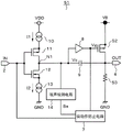
fig. 1 is a diagram schematically showing a configuration of a signal output circuit according to the first embodiment.
Fig. 2 is a diagram showing a specific configuration of the noise detection circuit.
Fig. 3 is a diagram showing a specific configuration of the malfunction prevention circuit.
Fig. 4 is a diagram showing a truth table of a logic circuit constituting the malfunction prevention circuit.
Fig. 5 is a waveform diagram for explaining each part of the noise detection operation.
Fig. 6 is a waveform diagram for explaining respective parts for stopping the forced driving operation.
Fig. 7 is a waveform diagram showing an output signal.
Fig. 8 is a diagram showing a specific configuration of a noise detection circuit according to the second embodiment.
Fig. 9 is a diagram showing a specific configuration example of the voltage conversion unit.
Fig. 10 is a waveform diagram for explaining each part of the noise detection operation.
Fig. 11 is a diagram showing a specific configuration of a noise detection circuit according to the third embodiment.
Fig. 12 is a waveform diagram for explaining each part of the noise detection operation.
Fig. 13 is a diagram schematically showing a configuration of a signal output circuit in which a configuration of an output stage is changed.
Fig. 14 is a diagram showing another specific configuration example of the voltage conversion unit.
Fig. 15 is a second diagram showing another specific configuration example of the voltage conversion unit.
Detailed Description
Hereinafter, a plurality of embodiments will be described with reference to the drawings. In the embodiments, substantially the same components are denoted by the same reference numerals, and description thereof is omitted.
(first embodiment)
Next, a first embodiment will be described with reference to fig. 1 to 7.
As shown IN fig. 1, the signal output circuit 1 controls the driving of the N-channel MOS transistor 3 based on a control signal IN input from the outside through an input terminal 2, thereby outputting an output signal OUT at a level corresponding to the level of the control signal IN from an output terminal 4. The control signal IN and the output signal OUT are both digital signals that represent 2 values at two voltage levels of a high level (hereinafter referred to as an H level) and a low level (hereinafter referred to as an L level). Thus, the above-mentioned levels correspond to voltage levels.
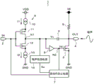
The transistor 3 corresponds to an output transistor, and has a source connected to a ground GND which is a reference potential of the circuit, a drain connected to the output terminal 4, and a power supply VB via a resistor 5. The power supply VB is supplied from a battery, not shown, for example, and has a stable voltage value of about + 12V.
The driving of the transistor 3 is controlled by a Slope control circuit (Slope control circuit)6 or a malfunction prevention circuit 7. Therefore, the gate of the transistor 3 is connected to the node N1 to which the output of the slope control circuit 6 is supplied, and to the node N2 to which the output of the malfunction prevention circuit 7 is supplied, via the buffer 8. The drain of the transistor 3 corresponds to one main terminal, and the gate corresponds to the on control terminal. A capacitor 9 is connected between the output terminal 4 and the node N1. The capacitor 9 corresponds to a feedback capacitance, and of the two terminals, the terminal on the output terminal 4 side corresponds to a first terminal, and the terminal on the node N1 side corresponds to a second terminal.
The slope control circuit 6 includes a current source 10, a P-channel MOS transistor 11, an N-channel MOS transistor 12, and a current source 13 connected in series between a power supply VDD and a ground GND. The power supply VDD is a power supply for operating the signal output circuit 1, and has a stable voltage of about + 5V. The transistors 11 and 12 have drains connected to the node N1, and gates connected to the input terminal 2. The input terminal 2 is supplied with a control signal IN from a control circuit, not shown, for controlling the operation of the signal output circuit 1.
With the above configuration, the slope control circuit 6 charges the capacitor 9 when the control signal IN is at the L level, and discharges the capacitor 9 when the control signal IN is at the H level. The voltage Vc of the second terminal of the capacitor 9 thus charged and discharged is supplied to the gate of the transistor 3 via the buffer 8. Therefore, the transistor 3 is driven by the voltage Vc that varies with the charge and discharge of the capacitor 9, and as a result, the Slope (Slope) of the output signal OUT is controlled. The values of the currents I1 and I2 output by the current sources 10 and 13 are appropriately set in accordance with the control amount of the desired slope, that is, the inclination of the desired output signal OUT.
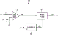
The noise detection circuit 14 indirectly detects noise superimposed on the output terminal OUT based on the voltage Vc, and determines whether the noise has periodicity. The noise detection signal Sa output from the noise detection circuit 14 is supplied to the malfunction prevention circuit 7. When periodic noise is detected, the noise detection signal Sa becomes H level. Specifically, the noise detection circuit 14 may include a comparison circuit 15, a counter 16, a periodicity determination unit 17, and a detection cancellation unit 18, as shown in fig. 2. The comparator circuit 15, the counter 16, the periodicity determining unit 17, and the detection canceling unit 18 all operate by receiving the power supply VDD.
The comparator circuit 15, which is composed of a comparator or the like, compares the voltage Vc with the voltage Vth, and outputs a pulse signal Sb inverted when the voltage Vc reaches the voltage Vth. The voltage Vth is switched according to the level of the control signal IN. Specifically, the period during which the control signal IN is at the H level, that is, the off period of the transistor 3, is set to a voltage higher than the steady value of the voltage Vc during the period and lower than the value of the voltage Vc at the time when the transistor 3 starts to be turned on. IN addition, during a period IN which the control signal IN is at the L level, that is, during the on period of the transistor 3, the voltage Vc is set to a voltage lower than the steady value of the voltage Vc during the period and higher than the value of the voltage Vc at the time when the transistor 3 starts to turn off.
The counting unit 16, which is configured by a counter or the like, counts the number of rising edges or falling edges of the pulse signal Sb, that is, the number of pulses of the pulse signal Sb. When noise having periodicity is superimposed, the period of the pulse signal Sb counted by the counting unit 16 is substantially equal to the period of the noise. Therefore, the count number of the counter 16 corresponds to the number of cycles of the noise. The periodicity determining unit 17, which is configured by a logic circuit or the like, sets the noise detection signal Sa to the H level when the count number (count value cnt) of the counting unit 16 is equal to or more than a predetermined number, for example, 4 times or more.
The detection canceling unit 18, which is configured by a logic circuit or the like, starts measurement of a predetermined end determination period Ta from a time point when the voltage Vc reaches the voltage Vth and the pulse signal Sb is inverted. The measurement of the end determination period Ta is performed based on the clock signal CLK. When the inversion of the pulse signal Sb is not present at all within the end determination period Ta, the detection canceling unit 18 outputs the canceling signal Sc. When the pulse signal Sb is inverted within the end determination period Ta, the detection canceling unit 18 resets the measurement value to zero at this point in time, and restarts the measurement of the end determination period Ta. When the cancel signal Sc is input, the periodicity determining unit 17 sets the noise detection signal Sa to L level.
The malfunction prevention circuit 7 performs a forced driving operation when the noise detection signal Sa supplied from the noise detection circuit 14 is at the H level. The forced driving operation is an operation of driving the transistor 3 so as to output the output signal OUT at a level corresponding to the level of the control signal IN, regardless of the driving of the transistor 3 by the slope control circuit 6. That is, when the noise detection circuit 14 detects periodic noise, the malfunction prevention circuit 7 performs a forced driving operation.
When the noise detection signal Sa is at the L level, the malfunction prevention circuit 7 stops the execution of the forced driving operation. That is, the malfunction prevention circuit 7 does not perform the forced driving operation during the period in which the noise detection circuit 14 does not detect noise and during the period in which noise having no periodicity is detected. After the start of the forced driving operation, the malfunction prevention circuit 7 ends the forced driving operation if the determination period Ta continues to end in a state where the noise detection circuit 14 does not detect noise.
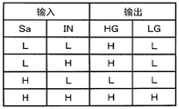
Specifically, the malfunction prevention circuit 7 may include a CMOS circuit 19 and a logic circuit 20 as shown in fig. 3. The P-channel MOS transistor 21 and the N-channel MOS transistor 22 constituting the CMOS circuit 19 are connected in series between the power supply VDD and the ground GND. The drains of the transistors 21 and 22 are connected to the gate of the transistor 3. The gates of the transistors 21 and 22 are supplied with the drive signals HG and LG output from the logic circuit 20, respectively.
The logic circuit 20 is input with a noise detection signal Sa and a control signal IN. The logic circuit 20 generates and outputs the drive signals HG and LG based on the input signals Sa and IN. Specifically, as shown IN fig. 4, when the noise detection signal Sa is at the L level, the logic circuit 20 outputs the drive signals HG and LG for turning off both the transistors 21 and 22 regardless of the level of the control signal IN. That is, when the noise detection signal Sa is at the L level, the forced driving operation is not performed.
When the noise detection signal Sa is at the H level, the logic circuit 20 turns on one of the transistors 21 and 22 IN accordance with the level of the control signal IN, and forcibly drives the transistor 3 to be on or off. That is, when the noise detection signal Sa is at the H level, the forced driving operation is performed.
Next, the operation of the above-described structure will be described.
[1] Action without superimposed noise
When no noise is superimposed on the output terminal 4, the noise detection signal Sa is at the L level, and therefore the forced driving operation of the malfunction prevention circuit 7 is not performed. Thus, the driving of the transistor 3 is controlled by the slope control circuit 6. Therefore, the signal output circuit 1 outputs the output signal OUT whose slope is controlled at a level corresponding to the level of the control signal IN.
[2] Action with superimposed noise having no periodicity
Even if noise having no periodicity is superimposed on the output terminal 4, the noise detection signal Sa is at the L level, and therefore, the forced driving operation of the malfunction prevention circuit 7 is not performed. Therefore, the signal output circuit outputs the output signal OUT whose slope is controlled at a level corresponding to the level of the control signal IN, as IN the case where no noise is superimposed.
[3] Action when noise having periodicity is superimposed
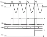
Here, an example is assumed IN which periodic noise is superimposed on the output terminal 4 while the control signal IN is at the H level, that is, while the transistor 3 is driven off to output the output signal OUT at the H level. As shown in fig. 5, if noise having periodicity is superimposed on the output terminal 4, the voltage Vc repeatedly rises and falls across the voltage Vth due to the influence of the noise. Thus, the comparator circuit 15 outputs the pulse signal Sb having the number of pulses corresponding to the number of cycles of the noise.
Then, when the count number of times of the counting section 16 reaches 4 times, the noise detection signal Sa transitions to the H level. Accordingly, the malfunction prevention circuit 7 performs a forced driving operation. In this case, the gate voltage Vg of the transistor 3 is fixed to the L level (═ GND), and the transistor 3 is driven to be off. The signal output circuit 1 outputs an output signal OUT of a level corresponding to the level of the control signal IN. However, the output signal OUT at this time is not subjected to slope control.
[4] Action when forced driving action is released
Here, it is assumed that the occurrence of noise converges after the forced driving operation is started as described above. As shown in fig. 6, if the superposition of the noise disappears, the pulse of the pulse signal Sb disappears. The detection canceling unit 18 starts to end the measurement of the determination period Ta from the falling time point t1 of the last pulse in the pulse signal Sb.
Then, if a state in which there is no superposition of noise until the end of the measurement of the end determination period Ta, that is, a state in which there is no pulse of the pulse signal Sb continues, the detection canceling unit 18 outputs the cancellation signal Sc at a time point t2 at which the measurement ends. Accordingly, the periodic determination unit 17 sets the noise detection signal Sa to the L level, and as a result, the malfunction prevention circuit 7 ends the forced driving operation. Therefore, the signal output circuit 1 outputs the output signal OUT whose slope is controlled at a level corresponding to the level of the control signal IN.
According to the signal output circuit 1 of the present embodiment described above, the following effects can be obtained.
If noise is superimposed on the output terminal 4, a forced driving operation of the malfunction prevention circuit 7 is performed. Therefore, even if the superimposed noise propagates to the slope control circuit 6 through the capacitor 9 and the noise affects the operation of the slope control circuit 6, a malfunction in which the output signal OUT becomes an unintended level does not occur. That is, even if noise is superimposed on the output terminal 4, the signal output circuit 1 simply loses the slope control, and can continue the main operation of the signal output circuit 1 that outputs the output signal OUT at a level corresponding to the level of the control signal IN.
However, even if the forced driving operation is performed, the slope of the output signal OUT is not necessarily lost. This is because, even when the forced driving operation is performed during a period in which the level of the output signal OUT does not change, that is, during a period in which the output signal OUT is stable at the H level or the L level, as in the period Tb in fig. 7, the signal output circuit 1 can output the output signal OUT having a waveform with a slope as in the case of the stable operation.
On the other hand, if the forced driving operation is performed during a period in which the level of the output signal OUT changes, i.e., during a period in which the output signal OUT rises or falls, as in the periods Tc and Td in fig. 7, the slope of the output signal OUT is lost, and a waveform having a sharp rise or fall is obtained. However, it is considered that the surroundings of the signal output circuit 1 are a noise environment when the forced driving operation is performed. In such an environment, since there is a low necessity to suppress noise radiated from the circuit to a low level, even if the slope control of the signal output circuit 1 is lost and the radiated noise increases, a significant problem does not occur.
The noise detection circuit 14 and the malfunction prevention circuit 7 are configured by elements that operate using the same power supply VDD as the other circuits configuring the signal output circuit 1. Therefore, according to the signal output circuit 1, even when the output-side voltage is higher than the operating voltage of the circuit as in the present embodiment, it is not necessary to use an element having a high withstand voltage, and an increase in the circuit scale can be suppressed. Further, in the signal output circuit 1, a current mirror circuit for determining the voltage of the output terminal 4 is not necessary, and therefore, the restriction that the minimum operating voltage becomes high does not occur.
The malfunction prevention circuit 7 performs a forced driving operation when the noise detection circuit 14 detects periodic noise. Therefore, it is possible to prevent a malfunction such as a forced driving operation from being performed based on erroneous detection of noise. For example, even if the voltage Vc overshoots (Overshoot) or undershoots (Undershoot) to reach the voltage Vth due to an operation such as normal slope control, the forced driving operation is not immediately performed.
In addition, the following effects can be obtained thereby. That is, when a single noise such as ESD (electrostatic Discharge) is superimposed on the output terminal 4, the forced driving operation of the malfunction prevention circuit 7 is not performed because the noise does not have periodicity. Therefore, the protection operation by the self-conduction of the transistor 3 is not hindered, and the surge current is easily discharged to the GND by the self-conduction. Thus, the internal circuit elements including the transistor 3 and the capacitor 9 can be protected from being damaged. That is, the internal circuit elements can be kept well resistant to damage by ESD or the like.
The noise detection circuit 14 is configured to detect a periodic noise using a counter 16 that counts the number of pulses of the pulse signal Sb and a periodic determination unit 17 that sets the noise detection signal Sa to an H level when the counted number of times is equal to or more than a predetermined number. These structures can be constituted by counters and small-scale logic circuits. Therefore, the increase in the circuit scale of the noise detection circuit 14 and thus the signal processing circuit 1 can be suppressed.
After the malfunction prevention circuit 7 starts the forced driving operation, if the noise is no longer detected, the forced driving operation is terminated. Thus, if the noise disappears, the slope control is promptly recovered, and the radiation of the noise from the signal output circuit 1 can be suppressed. In this case, the signal output circuit 1 is configured to end the forced driving operation when the state in which the noise is not detected continues to end the determination period Ta. With this configuration, it is possible to prevent the malfunction prevention circuit 7 from repeating the execution and termination of the forced driving operation when noise intermittently generated at relatively short intervals is superimposed.
The signal output circuit 1 can be applied to a communication driver for vehicle-mounted communication, for example, a LIN communication driver. In this case, the noise is assumed to be sinusoidal noise of about 1MHz to 1GHz, and the cycle thereof is shorter than 1 μ s. As described above, the period of the pulse signal Sb counted by the counting unit 16 is substantially equal to the period of the noise. Therefore, when such noise is superimposed on the output terminal 4, the time required for the noise detection circuit 14 to detect the noise is estimated to be at most about 4 μ s.
On the other hand, the communication rate of LIN is about 10kHz, and the pulse width of a pulse signal used for the communication is about 50 μ s. Accordingly, when the signal output circuit 1 is applied to the communication driver of the LIN, the period required for the noise detection circuit 14 to determine that the noise superimposed on the output terminal 4 has periodicity is extremely short compared to the periodicity of communication.
Therefore, in the signal output circuit 1, even if the forced driving operation is performed after the periodic noise is detected, it is possible to prevent a malfunction in which a microcomputer or the like that receives the output signal OUT as the communication signal and performs some processing from erroneously determining the level of the output signal OUT, that is, occurrence of a so-called error.
In this case, the termination determination period Ta measured by the detection canceling unit 18 is preferably set to a period (for example, 8 μ s) shorter than the communication cycle. Accordingly, the slope control is promptly recovered after the noise disappears, and the noise radiated from the signal output circuit 1 can be appropriately suppressed.
The signal output circuit 1 has a structure in which the buffer 8 is interposed between the node N1 and the gate of the transistor 3. When noise is superimposed on the output terminal 4, the main path through which the noise propagates to the inside is the capacitor 9. However, a parasitic capacitance, not shown, exists between the drain and the gate of the transistor 3. Since the transistor 3 is provided in the output stage, the size thereof is increased to ensure the driving capability, and the parasitic capacitance is also relatively large. Therefore, the noise superimposed on the output terminal 4 may be propagated to an internal circuit such as the slope control circuit 6 via the parasitic capacitance. By providing the buffer 8 as described above, the propagation path of noise via the parasitic capacitance is cut off, and therefore, it is possible to prevent the occurrence of malfunction in which the transistor 3 malfunctions due to the influence of the noise and the output signal OUT becomes an unintended level. Further, by providing the buffer 8, the impedance of the gate node of the transistor 3 can be reduced, and the amplitude of noise can be suppressed.
(second embodiment)
Next, a second embodiment in which the specific configuration of the noise detection circuit is changed from the first embodiment will be described with reference to fig. 8 to 10.
As shown in fig. 8, the noise detection circuit 31 includes a voltage conversion unit 32, a comparison circuit 33, and a periodicity determination unit 34. When the voltage Vc changes due to noise superimposed on the output terminal 4, the voltage converter 32 generates a voltage Va that gradually increases every time the change occurs. That is, the voltage Va corresponds to the number of cycles of noise integrated.
As the voltage conversion unit 32, a configuration using a diode D1 and a capacitor C1 shown in fig. 9 can be employed.
The comparator circuit 33, which is configured by a comparator or the like, compares the voltage Va with the voltage Vth, and outputs a pulse signal Sd that becomes H level when the voltage Va reaches the voltage Vth. In this case, the voltage Vth corresponds to the determination voltage. The voltage Vth is switched according to the level of the control signal IN. Specifically, the control signal IN is set to a predetermined voltage higher than GND and lower than VDD while the control signal IN is at the H level. Further, the control signal IN is set to a predetermined voltage higher than VDD while at the L level. When the pulse signal Sd changes to the H level, the periodicity determining section 34 sets the noise detection signal Sa to the H level and outputs the reset signal Se. When the reset signal Se is supplied, the voltage conversion unit 32 resets the voltage Va to zero.
The periodicity determining unit 34 starts measurement of the reset period Te from the output timing point of the reset signal Se. The reset period Te is set to a period longer than a period required for the voltage Va to rise from zero to the voltage Vth when noise having periodicity is supposed to be superimposed on the output terminal 4. The periodicity judging section 34 holds the noise detection signal Sa at the H level if the pulse signal Sd again transitions to the H level before the measurement of the reset period Te ends, and starts the output of the reset signal Se and the measurement of the reset period Te again. The periodicity judging section 34 sets the noise detection signal Sa to the L level if the pulse signal Sd does not transition to the H level again before the measurement of the reset period Te ends.
Next, the operation of the above-described structure will be described.
[1] Action without superimposed noise
When no noise is superimposed on the output terminal 4, the voltage Va does not reach the voltage Vth, and the noise detection signal Sa is at the L level, so that the forced driving operation of the malfunction prevention circuit 7 is not performed. Therefore, the operation of the entire signal output circuit 1 at this time is the same as that of the first embodiment.
[2] Action with superimposed noise having no periodicity
Even if noise having no periodicity is superimposed on the output terminal 4, the noise detection signal Sa is at the L level because the voltage Va does not reach the voltage Vth, and therefore the forced driving operation of the malfunction prevention circuit 7 is not performed. However, there is a possibility that: since there is no frequent superposition of periodic noise, the voltage Va reaches the voltage Vth soon, and the noise detection signal Sa transitions to the H level. However, in this case, the voltage Va does not reach the voltage Vth again until the measurement of the reset period Te is completed, and the noise detection signal Sa transitions to the L level, so that the forced driving operation of the malfunction prevention circuit 7 is not continued. Therefore, the operation of the entire signal output circuit 1 at this time is the same as that of the first embodiment.
[3] Action when noise having periodicity is superimposed
Here, it is assumed that periodic noise is superimposed on the output terminal 4 while the control signal IN is at the H level. As shown in fig. 10, if a noise having periodicity is superimposed on the output terminal 4, the voltage Va gradually rises and reaches the voltage Vth in the near future. Then, the noise detection signal Sa transitions to the H level, and the malfunction prevention circuit 7 performs a forced driving operation. Further, a waveform of the voltage Va is schematically shown in fig. 10. When a configuration including a diode and a capacitor as shown in fig. 9 is used as the voltage conversion unit 32, the waveform of the actual voltage Va is a waveform in which the following states are repeated: the noise rises at a relatively steep slope while the noise is above GND, and falls at a relatively gentle slope while the noise is below GND.
In this case, the forced driving operation is continued because the voltage Va is again increased to the voltage Vth during the period until the measurement of the reset period Te by the periodicity determining unit 34 is completed, and the H level of the noise detection signal Sa is maintained. Therefore, the operation of the entire signal output circuit 1 at this time is the same as that of the first embodiment.
[4] Action when forced driving action is released
Here, it is assumed that the occurrence of noise converges after the forced driving operation is started as described above. If the superposition of the noise disappears, the voltage Va does not rise. Therefore, the voltage Va does not reach the voltage Vth during the period until the measurement of the reset period Te by the period determination unit 34 is completed, and the noise detection signal Sa transitions to the L level, so that the forced driving operation of the malfunction prevention circuit 7 is completed. Therefore, the operation of the entire signal output circuit 1 at this time is the same as that of the first embodiment.
The same effects as those of the first embodiment can be obtained by the present embodiment described above.
The noise detection circuit 31 detects the noise based on whether or not the voltage Va corresponding to the value obtained by integrating the number of cycles of the noise reaches the voltage Vth. Therefore, according to the present embodiment, it is possible to detect noise having a frequency sufficiently higher than the frequency characteristics of the comparator and the like constituting the comparison circuit 33, regardless of the frequency characteristics.
(third embodiment)
Next, a third embodiment in which the specific configuration of the noise detection circuit is changed from the first embodiment will be described with reference to fig. 11 and 12.
As shown in fig. 11, the noise detection circuit 41 is different from the noise detection circuit 14 of the first embodiment in that a periodicity determining unit 42 is provided instead of the counting unit 16 and the periodicity determining unit 17.
As shown in fig. 12, the periodicity determining unit 42 measures a predetermined periodicity determining period Tf from a time point t1 when the first pulse signal Sb is inverted. When the edge of the pulse signal Sb is continuously detected during the period determination period Tf, the period determination unit 42 sets the noise detection signal Sa to the H level at the end time point t2 of the measurement period.
With this configuration, the same operation and effect as those of the first embodiment can be obtained.
Further, according to the noise detection circuit 41 of the present embodiment, since whether or not a periodic noise is superimposed is determined based on whether or not the edge of the pulse signal Sb is continuously detected within the predetermined periodicity determination period Tf, the period required for the determination is fixed without depending on the period of the noise. As described above, according to the present embodiment, since the presence or absence of periodic noise can be detected within a predetermined period of time regardless of the period of noise, even when noise having a low frequency is superimposed, the time until the noise is detected does not become excessively long.
(other embodiments)
The present disclosure is not limited to the embodiments described above and shown in the drawings, and can be modified or expanded as follows.
The pulse width of the pulse signal Sb in the first and third embodiments changes in accordance with the period in which the voltage Vc exceeds the voltage Vth, in other words, the pulse width changes in accordance with the temporal change in noise. However, the pulse width of the pulse signal Sb may be fixed. For example, if a configuration is adopted in which the pulse signal is changed to the H level when the voltage Vc reaches the voltage Vth, and the pulse signal is changed to the L level after a predetermined fixed period of time has elapsed from that point in time, the pulse width of the pulse signal Sb can be fixed. In this way, the pulse signal Sb having a fixed pulse width is provided regardless of the noise variation, and therefore, pulse omission in which a pulse that must be generated is not generated does not occur.
In the above embodiments, the signal output circuit has been described as a configuration in which the N-channel MOS transistor 3 is used as the output transistor and the drain thereof is pulled up by the resistor 5, that is, a low-voltage side driving configuration, but the configuration of the output stage is not limited to this. For example, as in the signal output circuit 51 shown in fig. 13, a P-channel MOS transistor 52 may be used as an output transistor, and the drain thereof may be pulled down by a resistor 53, that is, a high-voltage side driving configuration may be employed.
The noise detection circuit may not determine whether the periodicity of the noise exists, when it is not considered that the malfunction due to the false detection of the noise does not have a problem, when the destruction resistance to ESD or the like is sufficient, or the like. That is, the forced driving operation may be performed immediately when it is detected that noise is superimposed on the output terminal 4.
When the influence of noise that propagates to the internal circuit via the parasitic capacitance of the output transistor is not considered, the buffer 8 may not be provided.
As a specific configuration of the voltage converting unit 32, for example, a configuration as shown in fig. 14 and 15 may be adopted. The structure of fig. 14 is obtained by adding a resistor R1 to the structure of fig. 9. The resistor R1 discharges the charge charged in the capacitor C1, and is connected in parallel with the capacitor C1. With this configuration, the operation of the periodic determination unit 34 for releasing the forced driving operation can be changed as follows.
That is, in the configuration of fig. 14, if the superposition of noise disappears, the charging of the capacitor C1 is stopped, and the voltage Va drops according to the RC time constant. Therefore, the periodicity determining unit 34 has the following configuration: the noise detection signal Sa is transitioned to the L level when the voltage Va falls to a threshold value such as the voltage Vth. In this way, the release of the forced driving operation can be realized with a simpler configuration. In this case, the release time until the forced driving operation is completed can be adjusted by setting the capacitance value of the capacitor C1, the resistance value of the resistor R1, the threshold value of the voltage Vth, and the like.
The structure of fig. 15 includes a diode D2, a capacitor C2, and a resistor R2. The diode D2 has the output node side connected as an anode between the input node to which the voltage Vc is supplied and the output node of the output voltage Va. The capacitor C2 is connected between the output node and ground. The resistor R2 is used to charge the capacitor C2 and is connected in parallel with the diode D2.
In this case, in a normal state where no noise is superimposed, the capacitor C2 is charged through the resistor R2, and the voltage Va becomes a voltage near VDD. Then, if noise is superimposed, the capacitor C2 is discharged through the diode D2 every time noise is superimposed, and the voltage Va gradually decreases. When the voltage Va reaches the voltage Vth, the noise detection signal Sa changes to the H level, and the malfunction prevention circuit 7 performs a forced driving operation.
Further, if such a configuration is adopted, the operation of the periodicity determining unit 34 for canceling the forced driving operation can be changed as follows. That is, in the configuration of fig. 15, if the superposition of noise disappears, the discharge of the capacitor C2 stops, and the voltage Va rises according to the RC time constant. Therefore, the periodicity determining unit 34 has the following configuration: the noise detection signal Sa is shifted to the L level when the voltage Va rises to a threshold value such as the voltage Vth. In this way, the release of the forced driving operation can be realized with a simpler configuration. In this case, the cancellation time can be adjusted by setting each circuit constant as in the configuration of fig. 14.
The present disclosure has been described in terms of embodiments, but it should be understood that the present disclosure is not limited to the embodiments, constructions. The present disclosure also includes various modifications and modifications within an equivalent range. In addition, various combinations and modes and other combinations and modes in which only one element is included, or more than one element or less than one element are included in the scope and the spirit of the present disclosure.
Claims (10)
1. A signal output circuit (1, 51) which controls driving of an output transistor (3, 52) based on a control signal inputted from the outside, and outputs an output signal having a level corresponding to the level of the control signal from an output terminal (4) connected to one main terminal of the output transistor, the signal output circuit comprising:
a noise detection circuit (14, 31, 41) that detects noise superimposed on the output terminal;
a feedback capacitor (9) having a first terminal and a second terminal, the first terminal being connected to the output terminal, and the second terminal being connected to the noise detection circuit;
a slope control circuit (6) that controls the slope of the output signal by charging and discharging the feedback capacitor in accordance with the level of the control signal and driving the output transistor using the voltage of the second terminal of the feedback capacitor; and
and a malfunction prevention circuit (7) that performs a forced driving operation in which the output transistor is driven so as to output the output signal at a level corresponding to the level of the control signal, regardless of the driving of the output transistor by the slope control circuit, when the noise is detected by the noise detection circuit.
2. The signal output circuit of claim 1,
the malfunction prevention circuit performs the forced driving operation when the noise detection circuit detects a periodic noise.
3. The signal output circuit of claim 2,
the noise detection circuit (14) is provided with: a counting unit (16) that counts the number of cycles of noise superimposed on the output terminal; and a periodicity determination unit (17) that determines that the noise has periodicity when the number of noise cycles counted by the counting unit is equal to or greater than a predetermined number.
4. The signal output circuit of claim 2,
the noise detection circuit (31) is provided with: a voltage conversion unit (32) that outputs a voltage that changes due to noise superimposed on the output terminal; and a periodicity determination unit (34) that determines that the noise has periodicity when the output voltage of the voltage conversion unit reaches a predetermined determination voltage.
5. The signal output circuit of claim 4,
the voltage conversion unit (32) is provided with capacitors (C1, C2) that are charged or discharged by a current generated by noise superimposed on the output terminal, and outputs the terminal voltage of the capacitors.
6. The signal output circuit of claim 2,
the noise detection circuit (41) is provided with a periodicity determination unit (42), and the periodicity determination unit (42) measures a predetermined periodicity determination period from the time point when the noise superimposed on the output terminal is first detected, and determines that the noise has periodicity when the noise is continuously detected within the periodicity determination period.
7. The signal output circuit of claim 2,
the output signal is a signal used in communication,
the period required for the noise detection circuit to determine that the noise superimposed on the output terminal has periodicity is shorter than the period of the communication.
8. The signal output circuit of claim 1,
the malfunction prevention circuit terminates the forced driving operation when the noise is not detected by the noise detection circuit after the forced driving operation is started.
9. The signal output circuit of claim 8,
the malfunction prevention circuit terminates the forced driving operation when a state in which the noise is not detected by the noise detection circuit continues for a predetermined termination determination period after the forced driving operation is started.
10. The signal output circuit according to any one of claims 1 to 9,
the circuit further comprises a buffer (8) connected between the second terminal of the feedback capacitor and the conduction control terminal of the output transistor.
Applications Claiming Priority (3)
| Application Number | Priority Date | Filing Date | Title |
|---|---|---|---|
| JP2016-038953 | 2016-03-01 | ||
| JP2016038953A JP6638474B2 (en) | 2016-03-01 | 2016-03-01 | Signal output circuit |
| PCT/JP2017/001215 WO2017149956A1 (en) | 2016-03-01 | 2017-01-16 | Signal output circuit |
Publications (2)
| Publication Number | Publication Date |
|---|---|
| CN108702149A CN108702149A (en) | 2018-10-23 |
| CN108702149B true CN108702149B (en) | 2022-03-22 |
Family
ID=59743720
Family Applications (1)
| Application Number | Title | Priority Date | Filing Date |
|---|---|---|---|
| CN201780014257.4A Active CN108702149B (en) | 2016-03-01 | 2017-01-16 | Signal output circuit |
Country Status (4)
| Country | Link |
|---|---|
| US (1) | US10425069B2 (en) |
| JP (1) | JP6638474B2 (en) |
| CN (1) | CN108702149B (en) |
| WO (1) | WO2017149956A1 (en) |
Families Citing this family (5)
| Publication number | Priority date | Publication date | Assignee | Title |
|---|---|---|---|---|
| JP6638474B2 (en) * | 2016-03-01 | 2020-01-29 | 株式会社デンソー | Signal output circuit |
| JP6988670B2 (en) * | 2018-04-24 | 2022-01-05 | 三菱電機株式会社 | Drive circuit, power module and power conversion system |
| JP6852719B2 (en) * | 2018-07-12 | 2021-03-31 | 株式会社デンソー | Signal output circuit |
| CN112260664B (en) * | 2020-11-03 | 2023-06-02 | 电子科技大学 | Digital filter and high-voltage driving circuit applying same |
| CN112671421B (en) * | 2020-12-24 | 2022-03-18 | 西安翔腾微电子科技有限公司 | Wide common mode input range receiving circuit with failure protection and method |
Citations (7)
| Publication number | Priority date | Publication date | Assignee | Title |
|---|---|---|---|---|
| JPS57166735A (en) * | 1981-04-08 | 1982-10-14 | Nec Corp | Driving circuit |
| JP2006067334A (en) * | 2004-08-27 | 2006-03-09 | Fujitsu Ten Ltd | Noise reduction device and receiver |
| CN1825445A (en) * | 2005-02-22 | 2006-08-30 | 松下电器产业株式会社 | Drive apparatus |
| JP2012114793A (en) * | 2010-11-26 | 2012-06-14 | Denso Corp | Communication driver circuit |
| WO2012132215A1 (en) * | 2011-03-31 | 2012-10-04 | ルネサスエレクトロニクス株式会社 | Serial communication device |
| CN204498098U (en) * | 2014-06-27 | 2015-07-22 | 松下神视株式会社 | output circuit, detecting sensor |
| CN105009452A (en) * | 2013-02-28 | 2015-10-28 | 日立汽车系统株式会社 | Load drive control device |
Family Cites Families (7)
| Publication number | Priority date | Publication date | Assignee | Title |
|---|---|---|---|---|
| JPH04222113A (en) | 1990-12-25 | 1992-08-12 | Matsushita Electric Works Ltd | Digital filter circuit |
| US7292075B2 (en) * | 2005-01-04 | 2007-11-06 | Ahmed Kamal Abdel-Hamid | Rail-to-rail pad driver with load independent rise and fall times |
| JP2006245977A (en) | 2005-03-03 | 2006-09-14 | Fuji Xerox Co Ltd | Pulse signal reproducing apparatus |
| ATE455395T1 (en) * | 2006-08-08 | 2010-01-15 | Semiconductor Components Ind | DRIVER CIRCUIT |
| JP2011151576A (en) | 2010-01-21 | 2011-08-04 | Nec Saitama Ltd | Signal detection circuit, and incorrect detection preventing method |
| JP6233270B2 (en) * | 2014-10-21 | 2017-11-22 | 株式会社デンソー | Protection circuit |
| JP6638474B2 (en) * | 2016-03-01 | 2020-01-29 | 株式会社デンソー | Signal output circuit |
-
2016
- 2016-03-01 JP JP2016038953A patent/JP6638474B2/en active Active
-
2017
- 2017-01-16 WO PCT/JP2017/001215 patent/WO2017149956A1/en active Application Filing
- 2017-01-16 CN CN201780014257.4A patent/CN108702149B/en active Active
- 2017-01-16 US US16/065,199 patent/US10425069B2/en active Active
Patent Citations (7)
| Publication number | Priority date | Publication date | Assignee | Title |
|---|---|---|---|---|
| JPS57166735A (en) * | 1981-04-08 | 1982-10-14 | Nec Corp | Driving circuit |
| JP2006067334A (en) * | 2004-08-27 | 2006-03-09 | Fujitsu Ten Ltd | Noise reduction device and receiver |
| CN1825445A (en) * | 2005-02-22 | 2006-08-30 | 松下电器产业株式会社 | Drive apparatus |
| JP2012114793A (en) * | 2010-11-26 | 2012-06-14 | Denso Corp | Communication driver circuit |
| WO2012132215A1 (en) * | 2011-03-31 | 2012-10-04 | ルネサスエレクトロニクス株式会社 | Serial communication device |
| CN105009452A (en) * | 2013-02-28 | 2015-10-28 | 日立汽车系统株式会社 | Load drive control device |
| CN204498098U (en) * | 2014-06-27 | 2015-07-22 | 松下神视株式会社 | output circuit, detecting sensor |
Also Published As
| Publication number | Publication date |
|---|---|
| JP2017158010A (en) | 2017-09-07 |
| US10425069B2 (en) | 2019-09-24 |
| WO2017149956A1 (en) | 2017-09-08 |
| US20190020332A1 (en) | 2019-01-17 |
| CN108702149A (en) | 2018-10-23 |
| JP6638474B2 (en) | 2020-01-29 |
Similar Documents
| Publication | Publication Date | Title |
|---|---|---|
| CN108702149B (en) | Signal output circuit | |
| US7057427B2 (en) | Power on reset circuit | |
| US4920282A (en) | Dynamic latch circuit for preventing short-circuit current from flowing during absence of clock pulses when under test | |
| JP5133804B2 (en) | Reset signal generation circuit | |
| JP6335069B2 (en) | Power-on reset circuit | |
| JP2007243922A (en) | Oscillation circuit | |
| WO2005020437A1 (en) | Semiconductor integrated circuit device and power supply voltage monitor system employing it | |
| US11296691B2 (en) | Power-on reset circuit with reset transition delay | |
| EP3154199B1 (en) | A new power-on reset circuit | |
| US20050184783A1 (en) | Short pulse rejection circuit | |
| US7221199B2 (en) | Circuit and method for generating level-triggered power up reset signal | |
| US7902898B2 (en) | Delay circuit | |
| EP0035345B1 (en) | A power-on reset circuit | |
| US9729138B1 (en) | Circuits and systems having low power power-on-reset and/or brown out detection | |
| WO2016063494A1 (en) | Protection circuit | |
| US6198318B1 (en) | Power-on-reset circuit | |
| JP2008092271A (en) | Delay circuit | |
| JP2022085364A (en) | Control device of switching power supply | |
| KR20210067685A (en) | Power-on reset signal generating device | |
| WO2017149957A1 (en) | Signal output circuit | |
| KR100189746B1 (en) | Signal output circuit for power on reset | |
| KR100313512B1 (en) | Power on detect circuit | |
| JPH0446011B2 (en) | ||
| JP5262981B2 (en) | Latch device and latch method | |
| JP2002100973A (en) | Power-on reset circuit |
Legal Events
| Date | Code | Title | Description |
|---|---|---|---|
| PB01 | Publication | ||
| PB01 | Publication | ||
| SE01 | Entry into force of request for substantive examination | ||
| SE01 | Entry into force of request for substantive examination | ||
| GR01 | Patent grant | ||
| GR01 | Patent grant |