CN107833552B - Gate driving unit, gate driving circuit, driving method of gate driving circuit and display device - Google Patents
Gate driving unit, gate driving circuit, driving method of gate driving circuit and display device Download PDFInfo
- Publication number
- CN107833552B CN107833552B CN201711145565.9A CN201711145565A CN107833552B CN 107833552 B CN107833552 B CN 107833552B CN 201711145565 A CN201711145565 A CN 201711145565A CN 107833552 B CN107833552 B CN 107833552B
- Authority
- CN
- China
- Prior art keywords
- pull
- node
- transistor
- module
- electrode
- Prior art date
- Legal status (The legal status is an assumption and is not a legal conclusion. Google has not performed a legal analysis and makes no representation as to the accuracy of the status listed.)
- Active
Links
Images


Classifications
-
- G—PHYSICS
- G09—EDUCATION; CRYPTOGRAPHY; DISPLAY; ADVERTISING; SEALS
- G09G—ARRANGEMENTS OR CIRCUITS FOR CONTROL OF INDICATING DEVICES USING STATIC MEANS TO PRESENT VARIABLE INFORMATION
- G09G3/00—Control arrangements or circuits, of interest only in connection with visual indicators other than cathode-ray tubes
- G09G3/20—Control arrangements or circuits, of interest only in connection with visual indicators other than cathode-ray tubes for presentation of an assembly of a number of characters, e.g. a page, by composing the assembly by combination of individual elements arranged in a matrix no fixed position being assigned to or needed to be assigned to the individual characters or partial characters
- G09G3/34—Control arrangements or circuits, of interest only in connection with visual indicators other than cathode-ray tubes for presentation of an assembly of a number of characters, e.g. a page, by composing the assembly by combination of individual elements arranged in a matrix no fixed position being assigned to or needed to be assigned to the individual characters or partial characters by control of light from an independent source
- G09G3/36—Control arrangements or circuits, of interest only in connection with visual indicators other than cathode-ray tubes for presentation of an assembly of a number of characters, e.g. a page, by composing the assembly by combination of individual elements arranged in a matrix no fixed position being assigned to or needed to be assigned to the individual characters or partial characters by control of light from an independent source using liquid crystals
- G09G3/3611—Control of matrices with row and column drivers
- G09G3/3674—Details of drivers for scan electrodes
-
- G—PHYSICS
- G09—EDUCATION; CRYPTOGRAPHY; DISPLAY; ADVERTISING; SEALS
- G09G—ARRANGEMENTS OR CIRCUITS FOR CONTROL OF INDICATING DEVICES USING STATIC MEANS TO PRESENT VARIABLE INFORMATION
- G09G3/00—Control arrangements or circuits, of interest only in connection with visual indicators other than cathode-ray tubes
- G09G3/20—Control arrangements or circuits, of interest only in connection with visual indicators other than cathode-ray tubes for presentation of an assembly of a number of characters, e.g. a page, by composing the assembly by combination of individual elements arranged in a matrix no fixed position being assigned to or needed to be assigned to the individual characters or partial characters
- G09G3/22—Control arrangements or circuits, of interest only in connection with visual indicators other than cathode-ray tubes for presentation of an assembly of a number of characters, e.g. a page, by composing the assembly by combination of individual elements arranged in a matrix no fixed position being assigned to or needed to be assigned to the individual characters or partial characters using controlled light sources
- G09G3/30—Control arrangements or circuits, of interest only in connection with visual indicators other than cathode-ray tubes for presentation of an assembly of a number of characters, e.g. a page, by composing the assembly by combination of individual elements arranged in a matrix no fixed position being assigned to or needed to be assigned to the individual characters or partial characters using controlled light sources using electroluminescent panels
- G09G3/32—Control arrangements or circuits, of interest only in connection with visual indicators other than cathode-ray tubes for presentation of an assembly of a number of characters, e.g. a page, by composing the assembly by combination of individual elements arranged in a matrix no fixed position being assigned to or needed to be assigned to the individual characters or partial characters using controlled light sources using electroluminescent panels semiconductive, e.g. using light-emitting diodes [LED]
- G09G3/3208—Control arrangements or circuits, of interest only in connection with visual indicators other than cathode-ray tubes for presentation of an assembly of a number of characters, e.g. a page, by composing the assembly by combination of individual elements arranged in a matrix no fixed position being assigned to or needed to be assigned to the individual characters or partial characters using controlled light sources using electroluminescent panels semiconductive, e.g. using light-emitting diodes [LED] organic, e.g. using organic light-emitting diodes [OLED]
- G09G3/3266—Details of drivers for scan electrodes
-
- G—PHYSICS
- G09—EDUCATION; CRYPTOGRAPHY; DISPLAY; ADVERTISING; SEALS
- G09G—ARRANGEMENTS OR CIRCUITS FOR CONTROL OF INDICATING DEVICES USING STATIC MEANS TO PRESENT VARIABLE INFORMATION
- G09G2310/00—Command of the display device
- G09G2310/02—Addressing, scanning or driving the display screen or processing steps related thereto
- G09G2310/0264—Details of driving circuits
- G09G2310/0267—Details of drivers for scan electrodes, other than drivers for liquid crystal, plasma or OLED displays
-
- G—PHYSICS
- G09—EDUCATION; CRYPTOGRAPHY; DISPLAY; ADVERTISING; SEALS
- G09G—ARRANGEMENTS OR CIRCUITS FOR CONTROL OF INDICATING DEVICES USING STATIC MEANS TO PRESENT VARIABLE INFORMATION
- G09G2310/00—Command of the display device
- G09G2310/02—Addressing, scanning or driving the display screen or processing steps related thereto
- G09G2310/0264—Details of driving circuits
- G09G2310/0286—Details of a shift registers arranged for use in a driving circuit
-
- G—PHYSICS
- G09—EDUCATION; CRYPTOGRAPHY; DISPLAY; ADVERTISING; SEALS
- G09G—ARRANGEMENTS OR CIRCUITS FOR CONTROL OF INDICATING DEVICES USING STATIC MEANS TO PRESENT VARIABLE INFORMATION
- G09G2310/00—Command of the display device
- G09G2310/08—Details of timing specific for flat panels, other than clock recovery
Landscapes
- Engineering & Computer Science (AREA)
- Physics & Mathematics (AREA)
- Computer Hardware Design (AREA)
- General Physics & Mathematics (AREA)
- Theoretical Computer Science (AREA)
- Chemical & Material Sciences (AREA)
- Crystallography & Structural Chemistry (AREA)
- Control Of Indicators Other Than Cathode Ray Tubes (AREA)
Abstract
本发明属于显示技术领域,具体涉及栅极驱动单元、栅极驱动电路及其驱动方法和显示装置。该栅极驱动电路的每一栅极驱动单元中:输入模块用于对上拉节点充电以将上拉节点的电压上拉为高电平;下拉控制模块用于将预下拉节点和下拉节点下拉为低电平;预下拉模块用于将下拉节点和预下拉节点在上拉节点充电前下拉为低电平;下拉模块用于将下拉节点下拉为低电平;降噪模块用于对上拉节点和输出端进行降噪;复位模块用于复位上拉节点和输出端的电压;输出模块用于输出第N级栅极驱动信号。该栅极驱动单元、电路及其方法,在上拉节点预充电之前,分别对下拉节点和预下拉节点下拉,从而将下拉节点和预下拉节点较上拉节点充电提前拉低,具有较高的信赖性。
This invention belongs to the field of display technology, specifically relating to gate driving units, gate driving circuits, driving methods, and display devices. In each gate driving unit of the gate driving circuit: an input module is used to charge the pull-up node to pull its voltage to a high level; a pull-down control module is used to pull the pre-pull-down node and the pull-down node to a low level; a pre-pull-down module is used to pull the pull-down node and the pre-pull-down node to a low level before the pull-up node is charged; a pull-down module is used to pull the pull-down node to a low level; a noise reduction module is used to reduce noise at the pull-up node and the output terminal; a reset module is used to reset the voltages of the pull-up node and the output terminal; and an output module is used to output the Nth level gate driving signal. This gate driving unit, circuit, and method pull down the pull-down node and the pre-pull-down node respectively before the pull-up node is pre-charged, thereby pulling the pull-down node and the pre-pull-down node low before the pull-up node is charged, resulting in high reliability.
Description
技术领域technical field
本发明属于显示技术领域,具体涉及一种栅极驱动单元、栅极驱动电路、栅极驱动电路的驱动方法和显示装置。The invention belongs to the field of display technology, and in particular relates to a gate driving unit, a gate driving circuit, a driving method of the gate driving circuit, and a display device.
背景技术Background technique
GOA(Gate driver On Array)技术,即在基板上集成薄膜晶体管(Thin FilmTransistor,简称TFT)组成的栅极驱动电路,由于GOA技术具有降低成本、提升模组工艺产量、利于实现窄边框等优点,因此得到越来越广泛的应用。GOA (Gate driver On Array) technology, that is, a gate drive circuit composed of a thin film transistor (Thin Film Transistor, TFT for short) on a substrate, because GOA technology has the advantages of reducing cost, improving module process output, and facilitating the realization of narrow borders, etc. Therefore, it is more and more widely used.
GOA栅极驱动电路设计的关键点在于移位寄存的实现和电路的信赖性。如图1所示,现有的栅极驱动电路在实际工作中,由于TFT特性存在阈值漂移(Vth Shift),导致相应信号存在一定的延迟(Delay),进而导致不同功能模块中的薄膜晶体管在不同时序阶段出现本不应同时开启却同时开启的情况,从而影响栅极驱动电路的信赖性。The key point of GOA gate drive circuit design lies in the realization of the shift register and the reliability of the circuit. As shown in Figure 1, in the actual operation of the existing gate drive circuit, due to the threshold shift (Vth Shift) of the TFT characteristics, the corresponding signal has a certain delay (Delay), which in turn leads to the thin film transistors in different functional modules. In different timing stages, situations that should not be turned on at the same time occur at the same time, thereby affecting the reliability of the gate drive circuit.
可见,设计一种能有效避免薄膜晶体管误开启,具有高信赖性的栅极驱动电路成为目前亟待解决的技术问题。It can be seen that designing a gate driving circuit with high reliability that can effectively prevent the thin film transistor from turning on by mistake has become a technical problem to be solved urgently at present.
发明内容SUMMARY OF THE INVENTION
本发明所要解决的技术问题是针对现有技术中上述不足,提供一种栅极驱动单元、栅极驱动电路、栅极驱动电路的驱动方法和显示装置,至少解决同一时间不同模块中薄膜晶体管误开启的问题,具有较高的信赖性。The technical problem to be solved by the present invention is to provide a gate driving unit, a gate driving circuit, a driving method for a gate driving circuit and a display device aiming at the above deficiencies in the prior art, at least solving the problem of thin film transistor errors in different modules at the same time. Open questions have high reliability.
解决本发明技术问题所采用的技术方案是该栅极驱动单元,所述栅极驱动单元包括输入模块、下拉控制模块、预下拉模块、下拉模块、降噪模块、复位模块和输出模块,其中:The technical solution adopted to solve the technical problem of the present invention is the gate drive unit, the gate drive unit includes an input module, a pull-down control module, a pre-pull-down module, a pull-down module, a noise reduction module, a reset module and an output module, wherein:
所述输入模块,分别连接所述下拉模块、所述输出模块和输入信号,用于对上拉节点充电以将上拉节点的电压上拉为高电平,所述上拉节点为所述输入模块与所述下拉模块和所述输出模块之间的连接点;The input module is connected to the pull-down module, the output module and the input signal respectively, and is used for charging the pull-up node to pull up the voltage of the pull-up node to a high level, and the pull-up node is the input a connection point between the module and the pull-down module and the output module;
所述下拉控制模块,分别连接所述预下拉模块、所述下拉模块和预设电源,用于将预下拉节点和下拉节点下拉为低电平,所述预下拉节点为所述下拉控制模块与所述预下拉模块、所述下拉模块之间的连接点,所述下拉节点为所述下拉控制模块与所述下拉模块、所述降噪模块之间的连接点;The pull-down control module is connected to the pre-pull-down module, the pull-down module and the preset power supply respectively, and is used to pull down the pre-pull-down node and the pull-down node to a low level, and the pre-pull-down node is the pull-down control module and the pull-down control module. a connection point between the pre-pull-down module and the pull-down module, and the pull-down node is a connection point between the pull-down control module, the pull-down module, and the noise reduction module;
所述预下拉模块,还分别连接所述下拉节点和参考电源,用于在所述预下拉信号的电压控制下,将所述下拉节点和所述预下拉节点在所述上拉节点充电前下拉为低电平;The pre-pull-down module is further connected to the pull-down node and a reference power supply, respectively, for pulling down the pull-down node and the pre-pull-down node before charging the pull-up node under the voltage control of the pre-pull-down signal is low level;
所述下拉模块,还连接参考电源,用于在所述上拉节点的电压控制下将所述下拉节点下拉为低电平;The pull-down module is also connected to a reference power supply, and is used to pull down the pull-down node to a low level under the voltage control of the pull-up node;
所述降噪模块,还连接所述上拉节点、输出端和参考电压,用于在所述下拉节点的电压控制下对所述上拉节点和输出端进行降噪;The noise reduction module is further connected to the pull-up node, the output terminal and the reference voltage, for performing noise reduction on the pull-up node and the output terminal under the voltage control of the pull-down node;
所述复位模块,分别连接所述上拉节点、输出端、重置信号和参考电压,用于在重置信号的控制下复位所述上拉节点和输出端的电压;The reset module is respectively connected to the pull-up node, the output terminal, the reset signal and the reference voltage, and is used for resetting the voltage of the pull-up node and the output terminal under the control of the reset signal;
所述输出模块,还与时钟信号连接,用于在时钟信号和所述上拉节点的电压控制下,通过输出端输出本级栅极驱动信号。The output module is also connected with a clock signal, and is used for outputting the gate driving signal of the current stage through the output end under the control of the clock signal and the voltage of the pull-up node.
优选的是,所述输入模块包括第一晶体管,所述第一晶体管的控制极和第一极与所述输入信号连接,第二极与所述上拉节点连接。Preferably, the input module includes a first transistor, a control electrode and a first electrode of the first transistor are connected to the input signal, and a second electrode is connected to the pull-up node.
优选的是,所述下拉控制模块包括第五晶体管和第六晶体管,其中:Preferably, the pull-down control module includes a fifth transistor and a sixth transistor, wherein:
所述第五晶体管,其控制极与其第一极和预设电源连接,第二极与所述预下拉节点连接;the control electrode of the fifth transistor is connected to the first electrode and the preset power supply, and the second electrode is connected to the pre-pull-down node;
所述第六晶体管,其控制极与所述预下拉节点连接,第一极与所述第五晶体管的第一极连接,第二极与所述下拉节点连接。The control electrode of the sixth transistor is connected to the pre-pull-down node, the first electrode is connected to the first electrode of the fifth transistor, and the second electrode is connected to the pull-down node.
优选的是,所述预下拉模块包括第十一晶体管和第十二晶体管,其中:Preferably, the pre-pull-down module includes an eleventh transistor and a twelfth transistor, wherein:
所述第十一晶体管,其控制极与预下拉信号连接,第一极与参考电源连接,第二极与所述预下拉节点连接;the eleventh transistor, the control electrode is connected to the pre-pull-down signal, the first electrode is connected to the reference power supply, and the second electrode is connected to the pre-pull-down node;
所述第十二晶体管,其控制极与预下拉信号连接,第一极与参考电源连接,第二极与所述下拉节点连接。The control electrode of the twelfth transistor is connected to the pre-pull-down signal, the first electrode is connected to the reference power supply, and the second electrode is connected to the pull-down node.
优选的是,所述下拉模块包括第七晶体管和第八晶体管,其中:Preferably, the pull-down module includes a seventh transistor and an eighth transistor, wherein:
所述第七晶体管,其控制极与所述上拉节点连接,第一极与所述参考电源连接,第二极与所述预下拉节点连接;a control electrode of the seventh transistor is connected to the pull-up node, a first electrode is connected to the reference power supply, and a second electrode is connected to the pre-pull-down node;
所述第八晶体管,其控制极与所述上拉节点连接,第一极与所述参考电源连接,第二极与所述下拉节点连接。The control electrode of the eighth transistor is connected to the pull-up node, the first electrode is connected to the reference power supply, and the second electrode is connected to the pull-down node.
优选的是,所述复位模块包括第二晶体管和第四晶体管,其中:Preferably, the reset module includes a second transistor and a fourth transistor, wherein:
所述第二晶体管,其控制极与复位信号连接,第一极与参考电源连接,第一极与所述上拉节点连接;the control pole of the second transistor is connected to the reset signal, the first pole is connected to the reference power supply, and the first pole is connected to the pull-up node;
所述第四晶体管,其控制极与复位信号连接,第一极与参考电源连接接,第二极与输出端连接。The control pole of the fourth transistor is connected with the reset signal, the first pole is connected with the reference power supply, and the second pole is connected with the output end.
优选的是,所述降噪模块包括第九晶体管和第十晶体管,其中:Preferably, the noise reduction module includes a ninth transistor and a tenth transistor, wherein:
所述第九晶体管,其控制极与所述下拉节点连接,第一极与参考电源连接,第二极与所述上拉节点连接;the control electrode of the ninth transistor is connected to the pull-down node, the first electrode is connected to the reference power supply, and the second electrode is connected to the pull-up node;
所述第十晶体管,其控制极与所述下拉节点连接,第一极与所述参考电源连接,第二极与输出端连接。The control electrode of the tenth transistor is connected to the pull-down node, the first electrode is connected to the reference power supply, and the second electrode is connected to the output end.
优选的是,所述输出模块包括第三晶体管和存储电容,其中:Preferably, the output module includes a third transistor and a storage capacitor, wherein:
所述第三晶体管,其控制极和所述存储电容的第一端与所述上拉节点连接,第一极与时钟信号连接,第二极与所述存储电容的第二端连接,第二极与所述存储电容的第二端的连接点为输出端。The control electrode of the third transistor and the first end of the storage capacitor are connected to the pull-up node, the first electrode is connected to the clock signal, the second electrode is connected to the second end of the storage capacitor, and the second electrode is connected to the second end of the storage capacitor. The connection point between the pole and the second end of the storage capacitor is the output end.
优选的是,所述输入模块、所述下拉控制模块、所述预下拉模块、所述下拉模块、所述降噪模块、所述复位模块和所述输出模块中的晶体管,为N型薄膜晶体管,或者为P型薄膜晶体管,或者为N型薄膜晶体管与P型薄膜晶体管的组合。Preferably, the transistors in the input module, the pull-down control module, the pre-pull-down module, the pull-down module, the noise reduction module, the reset module and the output module are N-type thin film transistors , or a P-type thin film transistor, or a combination of an N-type thin film transistor and a P-type thin film transistor.
一种栅极驱动电路,包括多个级联的栅极驱动单元,每一所述栅极驱动单元用于为一条栅线提供栅极驱动信号,其中,所述栅极驱动单元为上述的栅极驱动单元。A gate drive circuit, comprising a plurality of cascaded gate drive units, each of the gate drive units is used to provide a gate drive signal for a gate line, wherein the gate drive unit is the above-mentioned gate drive unit pole drive unit.
优选的是,第N-2级所述栅极驱动单元的输出信号与第N级所述栅极驱动单元的所述输入模块连接,第N-1级所述栅极驱动单元的输入信号与第N级所述栅极驱动单元的所述预下拉模块连接,第N+2级所述栅极驱动单元的输出信号与第N级所述栅极驱动单元的所述复位模块连接,其中,N为大于2的整数。Preferably, the output signal of the gate driving unit at the N-2 stage is connected to the input module of the gate driving unit at the N-th stage, and the input signal of the gate driving unit at the N-1 stage is connected to the input module of the gate driving unit at the N-1 stage. The pre-pull-down module of the gate driving unit of the Nth stage is connected, and the output signal of the gate driving unit of the N+2th stage is connected to the reset module of the gate driving unit of the Nth stage, wherein, N is an integer greater than 2.
一种上述的栅极驱动电路的驱动方法,包括像素保持阶段、预下拉阶段、下拉阶段、输入阶段、输出阶段和复位阶段,其中:A driving method for the above-mentioned gate driving circuit, comprising a pixel holding stage, a pre-pull-down stage, a pull-down stage, an input stage, an output stage and a reset stage, wherein:
所述输入阶段:所述输入模块接收第N-2级所述栅极驱动单元的所述输出模块的输出信号、并将该输出信号存储于所述上拉节点以对所述上拉节点充电;The input stage: the input module receives the output signal of the output module of the gate driving unit of the N-2th stage, and stores the output signal in the pull-up node to charge the pull-up node ;
所述输出阶段:在时钟信号的控制下,通过所述输出模块的输出端输出高电平;The output stage: under the control of the clock signal, the output terminal of the output module outputs a high level;
所述像素保持阶段,在所述下拉节点的电压控制下,对所述上拉节点和所述输出端进行降噪;In the pixel holding stage, under the voltage control of the pull-down node, noise reduction is performed on the pull-up node and the output terminal;
所述预下拉阶段:在第N-1级所述栅极驱动单元的输入信号的控制下,在所述上拉节点充电前预下拉所述预下拉节点和所述下拉节点的电压;the pre-pull-down stage: under the control of the input signal of the gate driving unit in the N-1th stage, pre-pull down the voltage of the pre-pull-down node and the pull-down node before charging the pull-up node;
所述下拉阶段:在所述上拉节点的电压控制下,下拉所述预下拉节点和所述下拉节点的电压;the pull-down stage: under the voltage control of the pull-up node, pull down the voltages of the pre-pull-down node and the pull-down node;
所述复位阶段:以第N+2级所述栅极驱动单元的所述输出模块的输出信号,并根据该输出信号拉低所述上拉节点和所述输出端的电压。The reset stage: using the output signal of the output module of the gate driving unit in the N+2 stage, and pulling down the voltage of the pull-up node and the output terminal according to the output signal.
优选的是,所述预下拉阶段中,在对所述上拉节点预充电的至少第N-1个充电周期,将所述下拉节点和所述预下拉节点的电压提前拉低。Preferably, in the pre-pull-down stage, the voltages of the pull-down node and the pre-pull-down node are pulled down in advance in at least the N-1th charging cycle of pre-charging the pull-up node.
优选的是,包括:Preferably, include:
在所述输入阶段,第一晶体管开启,在第N-2级所述栅极驱动单元的电压控制下,对所述上拉节点充电;In the input stage, the first transistor is turned on, and the pull-up node is charged under the voltage control of the gate driving unit in the N-2th stage;
在所述输出阶段,在时钟信号的控制下,第三晶体管开启,输出端输出第N级栅极驱动信号;In the output stage, under the control of the clock signal, the third transistor is turned on, and the output terminal outputs the Nth gate drive signal;
在所述像素保持阶段,交替为高电平的预设电源控制第五晶体管和第六晶体管开启,分别控制所述预下拉节点和所述下拉节点的电压,通过第九晶体管为所述上拉节点降噪,通过第十晶体管为所述输出端降噪;In the pixel holding stage, the preset power supply that is alternately high level controls the fifth transistor and the sixth transistor to turn on, respectively controls the voltage of the pre-pull-down node and the pull-down node, and the ninth transistor is used for the pull-up node noise reduction, noise reduction for the output terminal through the tenth transistor;
在所述预下拉阶段,第N-1级所述栅极驱动单元的输入信号有效,第十一晶体管开启,将所述预下拉节点拉低;以及,第十二晶体管开启,将所述下拉节点拉低;同时,使得第九晶体管和第十晶体管关闭;In the pre-pull-down stage, the input signal of the gate driving unit of the N-1th stage is valid, the eleventh transistor is turned on, and the pre-pull-down node is pulled down; and the twelfth transistor is turned on, and the pull-down node is turned on. The node is pulled low; at the same time, the ninth transistor and the tenth transistor are turned off;
在所述下拉阶段,在所述上拉节点的电压控制下,第七晶体管和第八晶体管开启,分别预下拉所述预下拉节点和所述下拉节点的电压;In the pull-down stage, under the control of the voltage of the pull-up node, the seventh transistor and the eighth transistor are turned on to pre-pull down the voltages of the pre-pull-down node and the pull-down node, respectively;
在所述复位阶段,复位信号有效,第二晶体管和第四晶体管开启,分别将所述上拉节点和所述输出端下拉至低电平。In the reset phase, the reset signal is valid, the second transistor and the fourth transistor are turned on, and the pull-up node and the output terminal are respectively pulled down to a low level.
优选的是,第N-2级所述栅极驱动单元的输出信号为第N级所述栅极驱动单元的输入信号,第N-1级所述栅极驱动单元的输入信号为第N级所述栅极驱动单元的预下拉信号,第N+2级所述栅极驱动单元的输出信号为第N级所述栅极驱动单元的复位信号。Preferably, the output signal of the gate driving unit in the N-2th stage is the input signal of the gate driving unit in the N-th stage, and the input signal of the gate driving unit in the N-1th stage is the Nth stage. The pre-pull-down signal of the gate driving unit, the output signal of the gate driving unit of the N+2th stage is the reset signal of the gate driving unit of the Nth stage.
一种显示装置,包括上述的栅极驱动电路。A display device includes the above-mentioned gate driving circuit.
本发明的有益效果是:本发明中的栅极驱动单元、栅极驱动电路和相应的驱动方法,在上拉节点预充电之前,分别对下拉节点和预下拉节点下拉,从而将下拉节点和预下拉节点较上拉节点充电提前拉低,具有较高的信赖性。The beneficial effects of the present invention are: in the gate driving unit, the gate driving circuit and the corresponding driving method in the present invention, before the pull-up node is precharged, the pull-down node and the pre-pull-down node are respectively pulled down, so that the pull-down node and the pre-pull-down node are pulled down respectively. The pull-down node is pulled down earlier than the pull-up node for charging, which has higher reliability.
附图说明Description of drawings
图1为现有技术中栅极驱动电路在信号延迟情况下的INPUT和PD时序图;1 is an INPUT and PD timing diagram of a gate drive circuit in the prior art under the condition of signal delay;
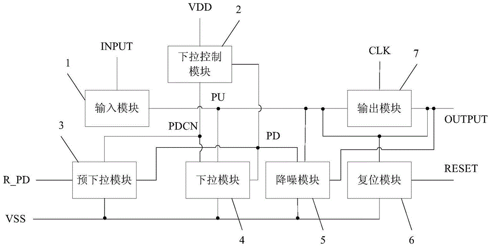
图2为本发明实施例1中栅极驱动单元的结构框图;2 is a structural block diagram of a gate driving unit in
图3为本发明实施例1中栅极驱动单元的电路原理示意图;3 is a schematic diagram of the circuit principle of the gate driving unit in
图4为本发明实施例1中栅极驱动电路的级联结构示意图;4 is a schematic diagram of a cascaded structure of a gate drive circuit in
图5为本发明实施例2中栅极驱动电路的时序图;5 is a timing diagram of a gate drive circuit in
图6为现有技术中栅极驱动电路的时序图;6 is a timing diagram of a gate drive circuit in the prior art;
附图标识中:In the attached drawings:
1-输入模块;2-下拉控制模块;3-预下拉模块;4-下拉模块;5-降噪模块;6-复位模块;7-输出模块。1-input module; 2-pull-down control module; 3-pre-pull-down module; 4-pull-down module; 5-noise reduction module; 6-reset module; 7-output module.
具体实施方式Detailed ways
为使本领域技术人员更好地理解本发明的技术方案,下面结合附图和具体实施方式对本发明栅极驱动单元、栅极驱动电路、栅极驱动电路的驱动方法和显示装置作进一步详细描述。In order to make those skilled in the art better understand the technical solutions of the present invention, the gate driving unit, the gate driving circuit, the driving method of the gate driving circuit and the display device of the present invention will be described in further detail below with reference to the accompanying drawings and specific embodiments. .
本发明的技术构思在于:根据现有技术中存在的不同模块不同阶段有同时开启的晶体管,造成信赖性降低的问题,设置使得可能因开启而影响信赖性的晶体管及时关闭的电路,即通过避免降噪模块中的晶体管与其他模块中的薄膜晶体管同时开启,提高信赖性。The technical idea of the present invention is: according to different modules existing in the prior art, there are transistors that are turned on at the same time at different stages, causing the problem of reduced reliability, and to set up a circuit that can turn off the transistors that may affect the reliability due to turning on in time, that is, by avoiding The transistors in the noise reduction module are turned on at the same time as the thin film transistors in other modules, improving reliability.
实施例1:Example 1:
本实施例提供一种栅极驱动单元及包括该栅极驱动单元的栅极驱动电路,该栅极驱动单元通过增加PD和PDCN的下拉级联设计,减小晶体管阈值偏移对栅极驱动电路的影响,从而提高其信赖性。This embodiment provides a gate drive unit and a gate drive circuit including the gate drive unit. The gate drive unit reduces the effect of transistor threshold shift on the gate drive circuit by adding a pull-down cascade design of PD and PDCN. influence, thereby increasing its reliability.
该栅极驱动电路包括多个级联的栅极驱动单元,每一栅极驱动单元用于为一条栅线提供栅极驱动信号。如图2所示,该栅极驱动单元包括输入模块1、下拉控制模块2、预下拉模块3、下拉模块4、降噪模块5、复位模块6和输出模块7,其中:The gate driving circuit includes a plurality of cascaded gate driving units, and each gate driving unit is used for providing a gate driving signal for one gate line. As shown in FIG. 2 , the gate driving unit includes an
输入模块1,分别连接下拉模块4、输出模块7和输入信号INPUT,用于对上拉节点PU充电以将上拉节点PU的电压上拉为高电平,上拉节点PU为输入模块1与下拉模块4和输出模块7之间的连接点;The
下拉控制模块2,分别连接预下拉模块3、下拉模块4和预设电源VDD,用于将预下拉节点PDCN和下拉节点PD下拉为低电平,预下拉节点PDCN为下拉控制模块2与预下拉模块3、下拉模块4之间的连接点,下拉节点PD为下拉控制模块2与下拉模块4、降噪模块5之间的连接点;The pull-
预下拉模块3,还分别连接下拉节点PD和参考电源VSS,用于在预下拉信号R_PD的电压控制下将下拉节点PD和预下拉节点PDCN在上拉节点PU充电前下拉为低电平;The pre-pull-down
下拉模块4,还连接参考电源VSS,用于在上拉节点PU的电压控制下将下拉节点PD下拉为低电平;The pull-
降噪模块5,还连接上拉节点PU、输出端OUTPUT和参考电压VSS,用于在下拉节点PD的电压控制下对上拉节点PU和输出端OUTPUT进行降噪;The
复位模块6,分别连接上拉节点PU、输出端OUTPUT、重置信号和参考电压,用于在重置信号的控制下复位上拉节点PU和输出端OUTPUT的电压;The
输出模块7,还与时钟信号CLK连接,用于在时钟信号CLK和上拉节点PU的电压控制下,通过输出端OUTPUT输出本级(即第N级,其中,N为大于2的整数)栅极驱动信号。The
该栅极驱动电路,通过避免降噪模块中的晶体管与其他模块中的薄膜晶体管同时开启,提高信赖性。栅极驱动单元中各模块的具体结构和连接关系如图3所示,以下将进行详细说明:The gate driving circuit improves reliability by preventing the transistors in the noise reduction module from being turned on simultaneously with the thin film transistors in other modules. The specific structure and connection relationship of each module in the gate drive unit is shown in Figure 3, and the following will be described in detail:
输入模块1引入输入信号INPUT,输入模块1包括第一晶体管M1,第一晶体管M1的控制极和第一极与输入信号INPUT连接,第二极与上拉节点PU连接。The
下拉控制模块2提供下拉控制,下拉控制模块2包括第五晶体管M5和第六晶体管M6,其中:The pull-
第五晶体管M5,其控制极与其第一极和预设电源VDD连接,第二极与预下拉节点PDCN连接;the control pole of the fifth transistor M5 is connected to its first pole and the preset power supply VDD, and its second pole is connected to the pre-pull-down node PDCN;
第六晶体管M6,其控制极与预下拉节点PDCN连接,第一极与第五晶体管M的第一极连接(即与预设电源VDD连接),第二极与下拉节点PD连接。The control electrode of the sixth transistor M6 is connected to the pre-pull-down node PDCN, the first electrode is connected to the first electrode of the fifth transistor M (ie, is connected to the preset power supply VDD), and the second electrode is connected to the pull-down node PD.
预下拉模块3提前将PD和PDCN拉低,从而提前关闭降噪模块5中的晶体管。预下拉模块3包括第十一晶体管M11和第十二晶体管M12,其中:The pre-pull-down
第十一晶体管M11,其控制极与预下拉信号R_PD连接,第一极与参考电源VSS连接,第二极与预下拉节点PDCN连接;The eleventh transistor M11 has a control pole connected to the pre-pull-down signal R_PD, a first pole connected to the reference power supply VSS, and a second pole connected to the pre-pull-down node PDCN;
第十二晶体管M12,其控制极与预下拉信号R_PD连接,第一极与参考电源VSS连接,第二极与下拉节点PD连接。The control electrode of the twelfth transistor M12 is connected to the pre-pull-down signal R_PD, the first electrode is connected to the reference power supply VSS, and the second electrode is connected to the pull-down node PD.
下拉模块4将PD和PDCN拉低,下拉模块4包括第七晶体管M7和第八晶体管M8,其中:The pull-
第七晶体管M7,其控制极与上拉节点PU连接,第一极与参考电源VSS连接,第二极与预下拉节点PDCN连接;the seventh transistor M7, the control pole of which is connected to the pull-up node PU, the first pole is connected to the reference power supply VSS, and the second pole is connected to the pre-pull-down node PDCN;
第八晶体管M8,其控制极与上拉节点PU连接,第一极与参考电源VSS连接,第二极与下拉节点PD连接.The control pole of the eighth transistor M8 is connected to the pull-up node PU, the first pole is connected to the reference power supply VSS, and the second pole is connected to the pull-down node PD.
复位模块6实现复位功能,复位模块6包括第二晶体管M2和第四晶体管M4,其中:The
第二晶体管M2,其控制极与复位信号RESET连接,第一极与参考电源VSS连接,第一极与上拉节点PU连接;The second transistor M2, the control pole of which is connected to the reset signal RESET, the first pole is connected to the reference power supply VSS, and the first pole is connected to the pull-up node PU;
第四晶体管M4,其控制极与复位信号RESET连接,第一极与参考电源VSS连接接,第二极与输出端OUTPUT连接。The control pole of the fourth transistor M4 is connected to the reset signal RESET, the first pole is connected to the reference power supply VSS, and the second pole is connected to the output terminal OUTPUT.
降噪模块5提供降噪功能,保证信号纯度。降噪模块5包括第九晶体管M9和第十晶体管M10,其中:The
第九晶体管M9,其控制极与下拉节点PD连接,第一极与参考电源VSS连接,第二极与上拉节点PU连接;The ninth transistor M9, the control pole of which is connected to the pull-down node PD, the first pole is connected to the reference power supply VSS, and the second pole is connected to the pull-up node PU;
第十晶体管M10,其控制极与下拉节点PD连接,第一极与参考电源VSS连接,第二极与输出端OUTPUT连接。The control electrode of the tenth transistor M10 is connected to the pull-down node PD, the first electrode is connected to the reference power supply VSS, and the second electrode is connected to the output terminal OUTPUT.
输出模块7输出本级(即第N级)栅极驱动信号,输出模块7包括第三晶体管M3和存储电容C,其中:The
第三晶体管M3,其控制极和存储电容C的第一端与上拉节点PU连接,第一极与时钟信号CLK连接,第二极与存储电容C的第二端连接,第二极与存储电容C的第二端的连接点为输出端OUTPUT。The third transistor M3, the control electrode and the first end of the storage capacitor C are connected to the pull-up node PU, the first electrode is connected to the clock signal CLK, the second electrode is connected to the second end of the storage capacitor C, and the second electrode is connected to the storage capacitor C. The connection point of the second end of the capacitor C is the output end OUTPUT.
其中,输入模块1、下拉控制模块2、预下拉模块3、下拉模块4、降噪模块5、复位模块6和输出模块7中的晶体管,为N型薄膜晶体管或者P型薄膜晶体管,此时,其第一极或第二极可以分别对应源极或者漏极;或者为N型薄膜晶体管与P型薄膜晶体管的组合。根据不同的应用场合,可以选用不同类型的薄膜晶体管,只需同时将选定类型的晶体管的端口极性按本实施例晶体管的端口极性在连接上做相应的改变即可,从而实现灵活控制,这里不再详述。The transistors in the
在进行多个栅极驱动单元级联时,前两级(即第N-2级)栅极驱动单元的输出信号与本级(即第N级)栅极驱动单元的输入模块1连接,前一级(即第N-1级)栅极驱动单元的输入信号INPUT与本级(即第N级)栅极驱动单元的预下拉模块3连接,第N+2级栅极驱动单元的输出信号与本级(即第N级)栅极驱动单元的复位模块6连接,从而形成多行驱动。When multiple gate driving units are cascaded, the output signals of the gate driving units of the first two stages (ie the N-2th stage) are connected to the
以4CLK模型为例,该栅极驱动电路中多个栅极驱动单元的级联如图4所示。n-2行的OUTPUT是n行GOA的INPUT,同时n+2行的OUTPUT是n行的RESET,n-3行的OUTPUT为n行的R_PD。Taking the 4CLK model as an example, the cascade connection of multiple gate drive units in the gate drive circuit is shown in Figure 4. The OUTPUT of row n-2 is the INPUT of the GOA of row n, while the OUTPUT of row n+2 is the RESET of row n, and the OUTPUT of row n-3 is the R_PD of row n.
本实施例的栅极驱动电路中,通过M11和M12,将n-3行的Ouput与R_PD连接,在INPUT信号给PU充电之前,提前将PD和PDCN拉低,提前关闭M9和M10,从而避免M1和M9同时开启的情况,从而能有效避免薄膜晶体管误开启,具有高信赖性。In the gate driving circuit of this embodiment, through M11 and M12, the Ouput of the n-3 row is connected to R_PD, and before the INPUT signal charges the PU, PD and PDCN are pulled down in advance, and M9 and M10 are turned off in advance, so as to avoid M1 and M9 are turned on at the same time, which can effectively prevent the thin film transistor from being turned on by mistake, and has high reliability.
实施例2:Example 2:
与实施例1的栅极驱动电路相对应,本实施例提供一种栅极驱动电路的驱动方法,能有效避免薄膜晶体管误开启,具有高信赖性。Corresponding to the gate driving circuit of the first embodiment, the present embodiment provides a driving method of the gate driving circuit, which can effectively prevent the thin film transistor from being turned on by mistake, and has high reliability.
根据图5所示的时序图,该驱动方法包括像素保持阶段、预下拉阶段、下拉阶段、输入阶段、输出阶段和复位阶段,其中:According to the timing diagram shown in FIG. 5 , the driving method includes a pixel retention stage, a pre-pull-down stage, a pull-down stage, an input stage, an output stage and a reset stage, wherein:
输入阶段:输入模块1接收前两级(即第N-2级)栅极驱动单元的输出模块7的输出信号作、并将该输出信号存储于上拉节点PU以对上拉节点PU充电;Input stage: the
输出阶段:在时钟信号CLK的控制下,通过输出模块7的输出端OUTPUT输出高电平;Output stage: under the control of the clock signal CLK, the output terminal OUTPUT of the
像素保持阶段,在下拉节点PD的电压控制下,对上拉节点PU和输出端OUTPUT进行降噪;In the pixel holding stage, under the control of the voltage of the pull-down node PD, noise reduction is performed on the pull-up node PU and the output terminal OUTPUT;
预下拉阶段:在前一级(即第N-1级)栅极驱动单元的输入信号INPUT的控制下,在上拉节点PU充电前预下拉预下拉节点PDCN和下拉节点PD的电压;Pre-pull-down stage: under the control of the input signal INPUT of the gate drive unit of the previous stage (ie, the N-1st stage), the voltages of the pre-pull-down node PDCN and the pull-down node PD are pre-pulled down before the pull-up node PU is charged;
下拉阶段:在上拉节点PU的电压控制下,下拉预下拉节点PDCN和下拉节点PD的电压;Pull-down stage: under the voltage control of the pull-up node PU, pull down the voltages of the pre-pull-down node PDCN and the pull-down node PD;
复位阶段:以第N+2级栅极驱动单元的输出模块7的输出信号,并根据该输出信号拉低上拉节点PU和输出端OUTPUT的电压。Reset stage: use the output signal of the
该栅极驱动电路的驱动方法,预下拉阶段中,在对上拉节点PU预充电的至少前一个(即第N-1个)充电周期,将下拉节点PD和预下拉节点PDCN的电压提前拉低,即通过预下拉模块3提前将PD和PDCN拉低,避免降噪模块5中的晶体管与其他模块中的薄膜晶体管同时开启,提高信赖性。图5中,相对于本级(即第N级)栅极驱动信号OUTPUT,下拉节点PD和预下拉节点PDCN提前了三个充电周期预下拉至低电平,上拉节点PU提前了两个充电周期进行预充电。In the driving method of the gate driving circuit, in the pre-pull-down stage, the voltages of the pull-down node PD and the pre-pull-down node PDCN are pulled up in advance in at least one charging cycle (ie, the N-1 th) before the pull-up node PU is pre-charged. Low, that is, the PD and PDCN are pulled down in advance by the pre-pull-down
该栅极驱动电路的驱动方法具体包括步骤:The driving method of the gate driving circuit specifically includes the steps:
在输入阶段,第一晶体管M1开启,在前两级(即第N-2级)栅极驱动单元的电压控制下,对上拉节点PU充电;In the input stage, the first transistor M1 is turned on, and the pull-up node PU is charged under the voltage control of the gate driving units of the first two stages (ie, the N-2th stage);
在输出阶段,在时钟信号CLK的控制下,第三晶体管M3开启,输出端OUTPUT输出本级(即第N级)栅极驱动信号;In the output stage, under the control of the clock signal CLK, the third transistor M3 is turned on, and the output terminal OUTPUT outputs the gate drive signal of the current stage (ie, the Nth stage);
在像素保持阶段,交替为高电平的预设电源VDD控制第五晶体管M5和第六晶体管M6开启,分别控制预下拉节点PDCN和下拉节点PD的电压,通过第九晶体管M9为上拉节点PU降噪,通过第十晶体管M10为输出端OUTPUT降噪。即,交替高电平的VDD控制PD,通过M9/M10一直给PU和OUTPUT降噪;In the pixel holding stage, the preset power supply VDD, which is alternately high level, controls the fifth transistor M5 and the sixth transistor M6 to turn on, respectively controls the voltages of the pre-pull-down node PDCN and the pull-down node PD, and the ninth transistor M9 is the pull-up node PU. Noise reduction, through the tenth transistor M10 to reduce noise for the output terminal OUTPUT. That is, the alternating high-level VDD controls the PD, and always reduces noise to the PU and OUTPUT through M9/M10;
在预下拉阶段,前一级(即第N-1级)栅极驱动单元的输入信号INPUT有效,第十一晶体管M11开启,将预下拉节点PDCN拉低;以及,第十二晶体管M12开启,将下拉节点PD拉低;同时,使得第九晶体管M9和第十晶体管M10关闭。即,R_PD信号为高电平,M11和M12开启,将PD和PDCN拉低,关闭M9和M10,如图5中的时间段b,通过预下拉模块3中的M11和M12提前将PD和PDCN拉低,从而提前关闭M9和M10;In the pre-pull-down stage, the input signal INPUT of the gate driving unit of the previous stage (ie, the N-1th stage) is valid, the eleventh transistor M11 is turned on, and the pre-pull-down node PDCN is pulled down; and the twelfth transistor M12 is turned on, The pull-down node PD is pulled down; at the same time, the ninth transistor M9 and the tenth transistor M10 are turned off. That is, when the R_PD signal is at a high level, M11 and M12 are turned on, PD and PDCN are pulled down, and M9 and M10 are turned off. Pull low, thereby closing M9 and M10 in advance;
在下拉阶段,在上拉节点PU的电压控制下,第七晶体管M7和第八晶体管M8开启,分别下拉预下拉节点PDCN和下拉节点PD的电压。该下拉阶段也即PU充电阶段,M1的栅极、源极为高电平,其开启给PU充电,M3开启,CLK为低电平,OUTPUT输出电平,即为VGH;在PU自举阶段,在存储电容C和M3 Cgs的自举作用下,PU点电位自举至约2VGH,消除M3的Vth漂移对输出信号的影响,实现更好的输出;In the pull-down stage, under the control of the voltage of the pull-up node PU, the seventh transistor M7 and the eighth transistor M8 are turned on to pull down the voltages of the pre-pull-down node PDCN and the pull-down node PD, respectively. This pull-down stage is also the PU charging stage. The gate and source of M1 are at a high level, which is turned on to charge the PU, M3 is turned on, CLK is at a low level, and the output level of OUTPUT is VGH; in the PU bootstrap stage, Under the bootstrapping action of the storage capacitor C and M3 Cgs, the potential of the PU point is bootstrapped to about 2VGH, which eliminates the influence of the Vth drift of M3 on the output signal and achieves better output;
在复位阶段,复位信号RESET有效,第二晶体管M2和第四晶体管M4开启,分别将上拉节点PU和输出端OUTPUT下拉至低电平。即RESET信号为高电平,M2和M4开启,将PU和OUTPUT拉至低电平。In the reset stage, the reset signal RESET is valid, the second transistor M2 and the fourth transistor M4 are turned on, and pull down the pull-up node PU and the output terminal OUTPUT to a low level, respectively. That is, the RESET signal is high, M2 and M4 are turned on, and PU and OUTPUT are pulled to low.
其中,前两级(即第N-2级)栅极驱动单元的输出信号为本级(即第N级)栅极驱动单元的输入信号INPUT,前一级(即第N-1级)栅极驱动单元的输入信号INPUT为本级(即第N级)栅极驱动单元的预下拉信号R_PD,第N+2级栅极驱动单元的输出信号为本级(即第N级)栅极驱动单元的复位信号RESET。即,n-2行的OUTPUT是n行的INPUT,n+2行的OUTPUT是n行的RESET;n-3行的OUTPUT为n行的R_PD,在INPUT信号给PU充电前,提前将PD和PDCN拉直低电平,关闭M9和M10。Among them, the output signal of the gate driving unit of the first two stages (ie the N-2th stage) is the input signal INPUT of the gate driving unit of this stage (ie the Nth stage), and the gate driving unit of the previous stage (ie the N-1th stage) The input signal INPUT of the pole driving unit is the pre-pull-down signal R_PD of the gate driving unit of this stage (ie, the Nth stage), and the output signal of the gate driving unit of the N+2th stage is the gate driving unit of this stage (ie, the Nth stage) Cell reset signal RESET. That is, the OUTPUT of row n-2 is the INPUT of row n, the OUTPUT of row n+2 is the RESET of row n; the OUTPUT of row n-3 is R_PD of row n, before the INPUT signal charges the PU, the PD and PDCN is pulled low, turning off M9 and M10.
在像素保持阶段,PDCN和PD为高电平,M9和M10开启,持续为GOA栅极驱动单元的PU和OUTPUT降噪。在PU充电、自举和复位阶段,即PU为高电平时,M7和M8开启,PDCN和PD电位被拉低,M9和M10关闭,栅极驱动单元正常输出。In the pixel holding phase, PDCN and PD are high, M9 and M10 are turned on, and continue to reduce noise for the PU and OUTPUT of the GOA gate drive unit. In the PU charging, bootstrapping and reset stages, that is, when the PU is at a high level, M7 and M8 are turned on, the PDCN and PD potentials are pulled down, M9 and M10 are turned off, and the gate drive unit outputs normally.
本实施例的栅极驱动电路的驱动方法中,在上拉节点PU预充电之前,分别对PD和PDCN下拉,从而将PD和PDCN较PU充电提前拉低,具有较高的信赖性。In the driving method of the gate driving circuit of this embodiment, before the pull-up node PU is precharged, PD and PDCN are pulled down respectively, so that PD and PDCN are pulled down earlier than PU charging, which has high reliability.
PD和PDCN点的拉低通过M7和M8进行,即当PU为高电平,M7和M8开启,PD和PDCN才被拉低,从而在PU预充电阶段,Input为高电平给PU充电,PU升为高电平,将PD和PDCN拉低,可见PU拉高与PD和PDCN拉低是同时的,各端点信号的时序图参考图5。The PD and PDCN points are pulled down through M7 and M8, that is, when the PU is at a high level, M7 and M8 are turned on, and PD and PDCN are pulled down. Therefore, in the PU pre-charging stage, the Input is at a high level to charge the PU. PU is raised to high level, and PD and PDCN are pulled down. It can be seen that PU is pulled up at the same time as PD and PDCN are pulled down. Refer to Figure 5 for the timing diagram of each endpoint signal.
而在现有技术中,并不设置预下拉模块,则根据当前的电路连接关系和驱动时序,如图6所示的时序图可知,PU电平上升沿和PD电平下降沿是同时的。在长时间工作后,GOA栅极驱动单元的晶体管Vth有不同程度的漂移,信号也会有相应的延迟,如图1所示考虑信号延迟之后的INPUT和PD信号。在时间段a内,INPUT为高电平,M1开启,INPUT给PU充电;同时PD为高电平,M9开启,PD给PU降噪;则存在将INPUT信号(即n-2行OUTPUT)拉低的风险。另外,实际工作中,TFT特性会有漂移,相应信号存在一定的延迟,因此通常会出现如图1所示的延迟:即INPUT信号有一定的延迟,在时间段a内,Input为高平,M1开启给PU充电;PU为高电平,理论上要M7和M8开启及时将PD和PDCN拉低;而实际产品中PD和PDCN点拉低需要一个过程,尤其在M7和M8 Vth存在漂移时,这个过程会延长。从而,会存在INPUT、PD和PDCN同时为高电平的时间段,此时M1和M9同时开启,将INPUT(即n-2行的output)拉低。经Smartspice模拟,也确实发现M7和M8的阈值Vth漂移量的余裕(margin)非常小,可接受的Vth漂移量小,从而影响其信赖性。However, in the prior art, a pre-pull-down module is not provided, and according to the current circuit connection relationship and driving timing, as shown in the timing diagram in FIG. 6 , the rising edge of the PU level and the falling edge of the PD level are simultaneous. After working for a long time, the transistor Vth of the GOA gate driving unit has different degrees of drift, and the signal will also have a corresponding delay. As shown in Figure 1, consider the INPUT and PD signals after the signal delay. During time period a, INPUT is high, M1 is turned on, INPUT charges the PU; at the same time, PD is high, M9 is turned on, and PD reduces noise to the PU; then there is a pull-up of the INPUT signal (ie, n-2 lines of OUTPUT). low risk. In addition, in actual work, the TFT characteristics will drift, and the corresponding signal has a certain delay, so the delay shown in Figure 1 usually occurs: that is, the INPUT signal has a certain delay, in the time period a, the Input is high level, M1 Turn on to charge PU; PU is high level, in theory, M7 and M8 must be turned on to pull down PD and PDCN in time; but in actual products, it takes a process to pull down PD and PDCN points, especially when M7 and M8 Vth drift, This process will be extended. Therefore, there will be a time period in which INPUT, PD, and PDCN are at a high level at the same time. At this time, M1 and M9 are turned on at the same time, pulling down INPUT (ie, the output of row n-2). Through Smartspice simulation, it is indeed found that the margin of the threshold Vth drift of M7 and M8 is very small, and the acceptable Vth drift is small, thus affecting their reliability.
可见,实施例1中的栅极驱动电路和实施例2中相应的驱动方法,即使长期使用过程中M7和M8的Vth有漂移,其栅极驱动电路也可以正常工作。而且,M11和M12的作用只是将PD和PDCN提前拉低,其需要的尺寸很小,对于边框影响非常小。It can be seen that the gate driving circuit in
由于目前车载、工控等显示产品为节省费用,需要采用GOA设计;同时其对显示面板信赖性高要求很高,需要采用高信赖性的GOA设计,本发明中的栅极驱动电路和相应的驱动方法能较好的应用于这些高信赖性要求场合。Because the current vehicle, industrial control and other display products need to adopt GOA design in order to save costs; at the same time, they have high requirements on the reliability of the display panel, and need to adopt the highly reliable GOA design, the gate driving circuit in the present invention and the corresponding driver The method can be better applied to these high reliability requirements.
实施例3:Example 3:
本实施例提供一种显示装置,该显示装置包括实施例1的栅极驱动电路,且采用实施例2中的栅极驱动电路的驱动方法。This embodiment provides a display device, which includes the gate driving circuit of the first embodiment, and adopts the driving method of the gate driving circuit of the second embodiment.
该显示装置可以为:台式电脑、平板电脑、笔记本电脑、手机、PDA、GPS、车载显示、投影显示、摄像机、数码相机、电子手表、计算器、电子仪器、仪表、液晶面板、电子纸、电视机、显示器、数码相框、导航仪等任何具有显示功能的产品或部件,可应用于公共显示和虚幻显示等多个领域。The display device can be: desktop computer, tablet computer, notebook computer, mobile phone, PDA, GPS, vehicle display, projection display, video camera, digital camera, electronic watch, calculator, electronic instrument, meter, liquid crystal panel, electronic paper, TV Any product or component with display function such as computer, monitor, digital photo frame, navigator, etc., can be used in many fields such as public display and unreal display.
该显示装置具有较好的显示品质。The display device has better display quality.
可以理解的是,以上实施方式仅仅是为了说明本发明的原理而采用的示例性实施方式,然而本发明并不局限于此。对于本领域内的普通技术人员而言,在不脱离本发明的精神和实质的情况下,可以做出各种变型和改进,这些变型和改进也视为本发明的保护范围。It can be understood that the above embodiments are only exemplary embodiments adopted to illustrate the principle of the present invention, but the present invention is not limited thereto. For those skilled in the art, without departing from the spirit and essence of the present invention, various modifications and improvements can be made, and these modifications and improvements are also regarded as the protection scope of the present invention.
Claims (16)
Priority Applications (4)
| Application Number | Priority Date | Filing Date | Title |
|---|---|---|---|
| CN201711145565.9A CN107833552B (en) | 2017-11-17 | 2017-11-17 | Gate driving unit, gate driving circuit, driving method of gate driving circuit and display device |
| US16/314,757 US11289039B2 (en) | 2017-11-17 | 2018-06-07 | Gate-driving unit circuit having pre-pull down sub-circuit, gate driver on array circuit, driving method, and display apparatus thereof |
| EP18847180.9A EP3714450A4 (en) | 2017-11-17 | 2018-06-07 | CIRCUIT FOR UNIT FOR GATE CONTROL, GATE DRIVER ON A MATRIX CIRCUIT, CONTROL PROCESS AND DISPLAY DEVICE |
| PCT/CN2018/090259 WO2019095679A1 (en) | 2017-11-17 | 2018-06-07 | Gate-driving unit circuit, gate driver on array circuit, driving method, and display apparatus |
Applications Claiming Priority (1)
| Application Number | Priority Date | Filing Date | Title |
|---|---|---|---|
| CN201711145565.9A CN107833552B (en) | 2017-11-17 | 2017-11-17 | Gate driving unit, gate driving circuit, driving method of gate driving circuit and display device |
Publications (2)
| Publication Number | Publication Date |
|---|---|
| CN107833552A CN107833552A (en) | 2018-03-23 |
| CN107833552B true CN107833552B (en) | 2020-09-25 |
Family
ID=61651883
Family Applications (1)
| Application Number | Title | Priority Date | Filing Date |
|---|---|---|---|
| CN201711145565.9A Active CN107833552B (en) | 2017-11-17 | 2017-11-17 | Gate driving unit, gate driving circuit, driving method of gate driving circuit and display device |
Country Status (4)
| Country | Link |
|---|---|
| US (1) | US11289039B2 (en) |
| EP (1) | EP3714450A4 (en) |
| CN (1) | CN107833552B (en) |
| WO (1) | WO2019095679A1 (en) |
Families Citing this family (17)
| Publication number | Priority date | Publication date | Assignee | Title |
|---|---|---|---|---|
| CN107833552B (en) * | 2017-11-17 | 2020-09-25 | 合肥鑫晟光电科技有限公司 | Gate driving unit, gate driving circuit, driving method of gate driving circuit and display device |
| CN108877716B (en) | 2018-07-20 | 2021-01-26 | 京东方科技集团股份有限公司 | Shift register unit and driving method thereof, gate driving circuit and display device |
| CN108766340B (en) * | 2018-08-06 | 2021-05-18 | 京东方科技集团股份有限公司 | Shifting register unit and driving method thereof, grid driving circuit and display device |
| CN108717846B (en) * | 2018-08-13 | 2021-04-16 | 惠科股份有限公司 | Shift register circuit and display device |
| CN108962121B (en) * | 2018-08-13 | 2021-04-16 | 惠科股份有限公司 | Shift register circuit and display device |
| CN111696490B (en) * | 2019-03-15 | 2025-03-04 | 合肥鑫晟光电科技有限公司 | Shift register unit and driving method thereof, gate driving circuit and display device |
| CN109872699B (en) * | 2019-04-15 | 2021-08-06 | 合肥鑫晟光电科技有限公司 | Shift register, gate drive circuit and display device |
| CN112309322B (en) * | 2019-07-31 | 2022-01-18 | 京东方科技集团股份有限公司 | Shift register and driving method thereof, grid driving circuit and display device |
| CN110599978B (en) * | 2019-09-19 | 2021-11-05 | 京东方科技集团股份有限公司 | Shift register, gate driving circuit and display device |
| CN110880301B (en) * | 2019-12-12 | 2022-07-01 | 京东方科技集团股份有限公司 | Shifting register, driving method thereof and grid driving circuit |
| CN111090195B (en) * | 2020-03-22 | 2020-06-23 | 深圳市华星光电半导体显示技术有限公司 | Display panel and electronic equipment |
| CN114495783A (en) * | 2020-10-27 | 2022-05-13 | 京东方科技集团股份有限公司 | Gate driving unit, gate driving circuit, gate driving method and display device |
| CN114220402B (en) * | 2021-09-29 | 2023-06-27 | 华映科技(集团)股份有限公司 | GIP circuit for improving splash screen and method thereof |
| US12354512B2 (en) * | 2022-04-28 | 2025-07-08 | Beijing Boe Optoelectronics Technology Co., Ltd. | Driving circuit, driving method and display device |
| US12205530B2 (en) * | 2022-09-26 | 2025-01-21 | Beijing Boe Optoelectronics Technology Co., Ltd. | Scan circuit and display apparatus |
| CN115512672B (en) * | 2022-10-25 | 2023-10-27 | 业成科技(成都)有限公司 | Scan driving circuit and operation method thereof |
| CN119400120A (en) * | 2024-12-24 | 2025-02-07 | 惠科股份有限公司 | Scanning drive circuit and display panel |
Citations (1)
| Publication number | Priority date | Publication date | Assignee | Title |
|---|---|---|---|---|
| CN102682699A (en) * | 2012-04-20 | 2012-09-19 | 京东方科技集团股份有限公司 | Grid electrode driving circuit and display |
Family Cites Families (18)
| Publication number | Priority date | Publication date | Assignee | Title |
|---|---|---|---|---|
| CN100410989C (en) * | 2005-03-22 | 2008-08-13 | 友达光电股份有限公司 | Pixel array and image quality improving method thereof |
| TWI394134B (en) * | 2008-12-12 | 2013-04-21 | Au Optronics Corp | Shift register with pre-pull-down circuit |
| CN101447232B (en) * | 2008-12-31 | 2012-01-11 | 友达光电股份有限公司 | Shift buffer of pre-pull-down forward stage surge |
| CN103050106B (en) * | 2012-12-26 | 2015-02-11 | 京东方科技集团股份有限公司 | Gate driving circuit, display module and displayer |
| CN103915052B (en) * | 2013-01-05 | 2017-05-10 | 北京京东方光电科技有限公司 | Grid driving circuit and method and display device |
| KR102060801B1 (en) * | 2013-04-25 | 2019-12-31 | 삼성디스플레이 주식회사 | Display device and image signal compensating method |
| CN103956146B (en) | 2014-04-17 | 2017-04-12 | 深圳市华星光电技术有限公司 | Liquid crystal panel drive circuit, liquid crystal display device and drive method |
| CN104732939A (en) * | 2015-03-27 | 2015-06-24 | 京东方科技集团股份有限公司 | Shifting register, grid drive circuit, display device and grid drive method |
| CN104700812A (en) * | 2015-03-31 | 2015-06-10 | 京东方科技集团股份有限公司 | Shifting register and array substrate grid drive device |
| CN104835475B (en) * | 2015-06-08 | 2017-03-29 | 京东方科技集团股份有限公司 | Shift register cell and its driving method, gate driver circuit and display device |
| CN105551421B (en) * | 2016-03-02 | 2019-08-02 | 京东方科技集团股份有限公司 | Shift register unit, driving method, gate driving circuit and display device |
| KR102457481B1 (en) * | 2016-04-14 | 2022-10-24 | 삼성디스플레이 주식회사 | Gate driving circuit and display device having the same |
| CN106448594B (en) * | 2016-10-24 | 2019-01-29 | 南京华东电子信息科技股份有限公司 | A high reliability gate drive circuit |
| CN106652933B (en) * | 2016-11-18 | 2021-02-26 | 南京中电熊猫液晶显示科技有限公司 | Grid drive circuit with forward and reverse scanning function |
| CN107068087B (en) * | 2017-03-31 | 2019-11-26 | 深圳市华星光电技术有限公司 | A kind of GOA driving circuit |
| TWI618042B (en) | 2017-05-19 | 2018-03-11 | 友達光電股份有限公司 | Driving circuit and display panel |
| CN107274856A (en) | 2017-08-22 | 2017-10-20 | 京东方科技集团股份有限公司 | A kind of shift register and its driving method, gate driving circuit |
| CN107833552B (en) * | 2017-11-17 | 2020-09-25 | 合肥鑫晟光电科技有限公司 | Gate driving unit, gate driving circuit, driving method of gate driving circuit and display device |
-
2017
- 2017-11-17 CN CN201711145565.9A patent/CN107833552B/en active Active
-
2018
- 2018-06-07 EP EP18847180.9A patent/EP3714450A4/en not_active Withdrawn
- 2018-06-07 US US16/314,757 patent/US11289039B2/en active Active
- 2018-06-07 WO PCT/CN2018/090259 patent/WO2019095679A1/en not_active Ceased
Patent Citations (1)
| Publication number | Priority date | Publication date | Assignee | Title |
|---|---|---|---|---|
| CN102682699A (en) * | 2012-04-20 | 2012-09-19 | 京东方科技集团股份有限公司 | Grid electrode driving circuit and display |
Also Published As
| Publication number | Publication date |
|---|---|
| US20210327377A1 (en) | 2021-10-21 |
| US11289039B2 (en) | 2022-03-29 |
| WO2019095679A1 (en) | 2019-05-23 |
| EP3714450A1 (en) | 2020-09-30 |
| EP3714450A4 (en) | 2021-06-16 |
| CN107833552A (en) | 2018-03-23 |
Similar Documents
| Publication | Publication Date | Title |
|---|---|---|
| CN107833552B (en) | Gate driving unit, gate driving circuit, driving method of gate driving circuit and display device | |
| CN108564930B (en) | Shift register and driving method thereof, grid driving circuit and display device | |
| US10891913B2 (en) | Shift register circuitry, gate driving circuit, and display device | |
| CN104464600B (en) | Shifting register unit, driving method of shifting register unit, shifting register circuit and display device | |
| CN102945657B (en) | Shift register unit, grid drive circuit, array substrate and display device | |
| CN108962154B (en) | Shifting register unit, array substrate grid driving circuit, display and grid driving method | |
| US10121437B2 (en) | Shift register and method for driving the same, gate driving circuit and display device | |
| CN107331418B (en) | Shift register and driving method thereof, grid driving circuit and display device | |
| KR101989721B1 (en) | Liquid crystal display device and gate driver thereof | |
| WO2020010852A1 (en) | Shift register unit, driving method, gate driving circuit, and display device | |
| CN107564459B (en) | Shift register unit, grid driving circuit, display device and driving method | |
| CN103413514A (en) | Shifting register unit, shifting register and displaying device | |
| CN103915074B (en) | A kind of shift register cell, gate drive apparatus and display panel | |
| WO2022089070A1 (en) | Shift register, gate driving circuit, and display panel | |
| CN204406959U (en) | Shift register cell, shift-register circuit and display device | |
| CN103489425A (en) | Level switching circuit, array substrate and display device | |
| CN107909959A (en) | Shift register cell, its driving method, gate driving circuit and display device | |
| CN106504719A (en) | Shift register cell, driving method, gate driver circuit and display device | |
| CN110648621B (en) | Shift register and driving method thereof, grid driving circuit and display device | |
| CN110534048B (en) | Shift register unit, driving method, gate driving circuit and display device | |
| CN105761758A (en) | Shifting register unit, driving method, grid driving circuit and display device | |
| CN108766381B (en) | Shift register circuit, array substrate and display device | |
| CN106952604A (en) | Shift register, gate driving circuit and its driving method, display device | |
| CN103165190A (en) | Shifting register units, shifting register, array substrate and display device | |
| US10438554B2 (en) | Shift register and driving method thereof, gate on array circuit and display apparatus |
Legal Events
| Date | Code | Title | Description |
|---|---|---|---|
| PB01 | Publication | ||
| PB01 | Publication | ||
| SE01 | Entry into force of request for substantive examination | ||
| SE01 | Entry into force of request for substantive examination | ||
| GR01 | Patent grant | ||
| GR01 | Patent grant |