CN107704403B - Device and method for optimizing signal transmission of main back plate - Google Patents
Device and method for optimizing signal transmission of main back plate Download PDFInfo
- Publication number
- CN107704403B CN107704403B CN201710900309.XA CN201710900309A CN107704403B CN 107704403 B CN107704403 B CN 107704403B CN 201710900309 A CN201710900309 A CN 201710900309A CN 107704403 B CN107704403 B CN 107704403B
- Authority
- CN
- China
- Prior art keywords
- slim
- interfaces
- cable
- signal
- main board
- Prior art date
- Legal status (The legal status is an assumption and is not a legal conclusion. Google has not performed a legal analysis and makes no representation as to the accuracy of the status listed.)
- Active
Links
- 238000000034 method Methods 0.000 title claims abstract description 20
- 230000008054 signal transmission Effects 0.000 title claims abstract description 12
- 101100439969 Arabidopsis thaliana CLPD gene Proteins 0.000 claims description 2
- 238000013461 design Methods 0.000 abstract description 7
- 238000004891 communication Methods 0.000 description 4
- 238000010586 diagram Methods 0.000 description 4
- 230000000694 effects Effects 0.000 description 3
- 239000000969 carrier Substances 0.000 description 2
- 238000003780 insertion Methods 0.000 description 2
- 230000037431 insertion Effects 0.000 description 2
- 238000012986 modification Methods 0.000 description 2
- 230000004048 modification Effects 0.000 description 2
- 238000012544 monitoring process Methods 0.000 description 2
- 230000009286 beneficial effect Effects 0.000 description 1
- 238000012545 processing Methods 0.000 description 1
- 239000007787 solid Substances 0.000 description 1
Images


Classifications
-
- G—PHYSICS
- G06—COMPUTING; CALCULATING OR COUNTING
- G06F—ELECTRIC DIGITAL DATA PROCESSING
- G06F13/00—Interconnection of, or transfer of information or other signals between, memories, input/output devices or central processing units
- G06F13/10—Program control for peripheral devices
- G06F13/12—Program control for peripheral devices using hardware independent of the central processor, e.g. channel or peripheral processor
- G06F13/124—Program control for peripheral devices using hardware independent of the central processor, e.g. channel or peripheral processor where hardware is a sequential transfer control unit, e.g. microprocessor, peripheral processor or state-machine
- G06F13/126—Program control for peripheral devices using hardware independent of the central processor, e.g. channel or peripheral processor where hardware is a sequential transfer control unit, e.g. microprocessor, peripheral processor or state-machine and has means for transferring I/O instructions and statuses between control unit and main processor
-
- G—PHYSICS
- G06—COMPUTING; CALCULATING OR COUNTING
- G06F—ELECTRIC DIGITAL DATA PROCESSING
- G06F2213/00—Indexing scheme relating to interconnection of, or transfer of information or other signals between, memories, input/output devices or central processing units
- G06F2213/0016—Inter-integrated circuit (I2C)
Landscapes
- Engineering & Computer Science (AREA)
- Theoretical Computer Science (AREA)
- Computer Hardware Design (AREA)
- Microelectronics & Electronic Packaging (AREA)
- Physics & Mathematics (AREA)
- General Engineering & Computer Science (AREA)
- General Physics & Mathematics (AREA)
- Communication Control (AREA)
- Cable Transmission Systems, Equalization Of Radio And Reduction Of Echo (AREA)
Abstract
The invention discloses a device and a method for optimizing signal transmission of a main backboard, wherein a circuit comprises a main board, a backboard and a cable for connecting the main board and the backboard, and the device is characterized in that: two ends of the cable are respectively connected with corresponding slim interfaces on the main board and the back board, a plurality of slim interfaces at the main board end are connected with an I2C signal output end of the CPU, and the back board end sends an I2C signal to the CPLD through the corresponding slim interfaces. The method comprises the steps that a main board and a back board are connected through a cable, and two ends of the cable are respectively connected with corresponding slim interfaces on the main board and the back board; and a plurality of slim interfaces at the end of the main board are all connected with an I2C signal output end of the CPU, and the CPLD selects an I2C channel to realize I2C analysis by judging the in-place signal of the newly added slim cable according to a set priority rule. The invention has simple design structure, makes the system configuration more flexible and improves the reliability of the system on the premise of not increasing the cost.
Description
Technical Field
The invention relates to the technical field of computers, in particular to a device and a method for optimizing signal transmission of a main back plate.
Background
As a new extensible storage application protocol, NVMe (Non-Volatile Memory standard) has the advantages of high IOPS (Input/Output Per connected, throughput), low latency, low power consumption, and the like, and can fully exert PCIe SSD (PCIe, a high-speed serial computer extended bus standard; SSD, Solid State Drives) performance, thereby achieving increasingly wide applications in enterprise-level and large-data scenarios.
The NVMe SSD is communicated with the CPU based on a PCIe bus, and the interconnection and intercommunication are realized by taking a high-speed cable and a back plate as carriers. As shown in fig. 1, in the backplane design, the CPU HP _ I2C signal is generally analyzed by a CPLD connected to the backplane through a first slim line0 interface to implement NVMe SSD lighting control.
This method requires that the first slim interface cable must be connected, if the cable is not connected or an unexpected condition occurs to cause a link disconnection, the I2C signal at the main board end cannot be transmitted to the back board CPLD (Complex Programmable Logic Device), other 3 normally operating NVMe SSD status lamps on the back board cannot be controlled, and the CPU cannot receive the hard disk on-site information at the back board end.
Disclosure of Invention
The invention aims to provide a device and a method for optimizing signal transmission of a main back board, which are used for solving the problem that I2C communication cannot be carried out between the main back boards under the condition that a certain slim interface cable is not connected or other links are accidentally disconnected.
The technical scheme adopted by the invention for solving the technical problems is as follows: a device for optimizing signal transmission of a main backboard comprises a main board, a backboard and a cable for connecting the main board and the backboard, wherein two ends of the cable are respectively connected with corresponding slim interfaces on the main board and the backboard, a plurality of slim interfaces at the main board end are all connected with an I2C signal output end of a CPU, and the backboard end sends an I2C signal to a CPLD through the corresponding slim interfaces.
Further, the slim line interface at the main board end is grounded, the slim line interface at the back board end is pulled up, and the CPLD gates an I2C signal channel by detecting a level signal of the slim line interface at the back board end.
Further, the backplane side slim interface is connected to a power supply VDD through a pull-up resistor.
A method for optimizing signal transmission of a main back plate comprises the following steps:
connecting the main board and the back board through a cable, wherein two ends of the cable are respectively connected with corresponding slim interfaces on the main board and the back board;
and connecting a plurality of slim interfaces at the end of the main board to the I2C signal output end of the CPU, and sending an I2C signal to the CPLD through the corresponding slim interfaces at the end of the back board.
Further, the method further comprises a step of gating the I2C signal at the backplane end, and the specific implementation process is as follows:
grounding a slim line interface at a mainboard end, and pulling up a slim line interface at a backboard end;
the CLPD gates an I2C channel by detecting the high and low of a slim interface level signal at the back plate end.
Further, the backplane side slim interface is connected to a power supply VDD through a pull-up resistor.
The effect provided in the summary of the invention is only the effect of the embodiment, not all the effects of the invention, and one of the above technical solutions has the following advantages or beneficial effects:
1. a plurality of slim interfaces on the mainboard are all connected with an I2C signal, the slim interfaces on the corresponding back plates are all connected with a CPLD, even if the slim _0 interfaces are in failure, I2C communication can still be carried out between the main back plates, the normal work of a computer is ensured, the design structure is simple, the system configuration is more flexible on the premise of not increasing the cost, and the reliability of the system is improved.
2. CPLD judgment logic is set for I2C channels of a plurality of slim interfaces, and normal and orderly work of the system is guaranteed. Potentially improving the product image and competitiveness.
Drawings
FIG. 1 is a schematic diagram of a main backplane connection in the prior art;
FIG. 2 is a schematic diagram of the interconnection topology of the main backplane of the present invention;
FIG. 3 is a schematic diagram of the main backplane connection of the present invention;
FIG. 4 is a schematic flow diagram of the method of the present invention.
Detailed Description
In order to clearly explain the technical features of the present invention, the following detailed description of the present invention is provided with reference to the accompanying drawings. The following disclosure provides many different embodiments, or examples, for implementing different features of the invention. To simplify the disclosure of the present invention, the components and arrangements of specific examples are described below. Furthermore, the present invention may repeat reference numerals and/or letters in the various examples. This repetition is for the purpose of simplicity and clarity and does not in itself dictate a relationship between the various embodiments and/or configurations discussed. It should be noted that the components illustrated in the figures are not necessarily drawn to scale. Descriptions of well-known components and processing techniques and procedures are omitted so as to not unnecessarily limit the invention.
The following examples are described with NVMe 4 ports as an example, but are equally applicable to design improvements of other NVMe port count backplanes.
As shown in fig. 2, the NVMe SSD communicates with the CPU based on the PCIe bus, and realizes interconnection and intercommunication by using the high-speed cable and the backplane as carriers. In the invention, a cable terminal (main board end) and a corresponding main board/back board high-speed interface (back board end) adopt a slim line interface which accords with SFF-9402 specification, and an interface which accords with SFF-8639 specification is adopted for connecting an SSD hard disk end.
In the backplane design of fig. 1, the I2C signal of the CPU is generally analyzed by the CPLD connected to the backplane through the first slim 0 interface to implement NVMe SSD lighting control.
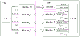
As shown in fig. 3, the apparatus for optimizing signal transmission of a main backplane of the present invention includes a main board, a backplane, and a cable (cable) connecting the main board and the backplane, where two ends of the cable are respectively connected to corresponding slim line interfaces on the main board and the backplane, for example, a slim line _0 interface at the main board end is connected to a slim line _0 interface at the backplane end. The slim interfaces on the mainboard end are all connected with the I2C signal output end of the CPU, and the backboard end sends the I2C signal to the CPLD through the corresponding slim interfaces. I.e., 4I 2C channels are all connected to the CPLD. At this time, even if the first or some other cable is not connected, the I2C signal at the host end still has a physical path to the backplane without affecting the communication between the two.
There are 4I 2C channels connected to the CPLD, which need the CPLD to select the channel for parsing. The solution of this embodiment is to select 1pin CPRNT # (CPRNT is an abbreviation of Cable Present, and # represents that this signal is active low) in the slim interface to be set as a judgment signal for judging whether the Cable is in place, and connect to the CPLD. The specific implementation scheme is that a main board end slim is connected with GND, a back board end slim is pulled up (high level), and the main board end slim is connected with a power supply VDD through a pull-up resistor to realize pull-up. If the cable is inserted, the pin at the backplane end becomes low level, and the CPLD receives the signal and becomes low, that is, knows that the cable is inserted into the interface.
The CPLD performs I2C channel selection by monitoring the cable in-place signal condition of 4 slim interfaces, and the priority level is reduced from slim _0 to slim _3 in sequence. The CPLD can know whether the cable is in place (inserted) by reading CPRNT # levels of 4 slim interfaces. Only one set of I2C is actually selected for resolution. For example, if a slim _0 cable insertion is detected, the slim _ 0I 2C signal is resolved, and the remaining I2C channels are not processed; if the slim _0 cable is inserted and it is detected that the slim _1 is inserted, the I2C of the slim _1 is analyzed, and so on. Therefore, the CPLD can automatically select the I2C analytic channel by judging the cable in-place condition, and the problem of limitation on a cable connection port in the design scheme before improvement is solved. Of course, the priority of the slim line can be customized and is within the scope of the present invention.
As shown in fig. 4, a method for optimizing signal transmission of a main backplane of the present invention includes the following steps:
s1, connecting the main board and the back board through a cable, wherein two ends of the cable are respectively connected with corresponding slim interfaces on the main board and the back board;
and S2, connecting the plurality of slim interfaces at the main board end with the I2C signal output end of the CPU, and sending the I2C signal to the CPLD through the slim interfaces corresponding to the back board end.
In step S1, the slim interfaces connecting the motherboard and the backplane are corresponding to each other, for example, the slim _0 interface at the motherboard end is connected to the slim _0 interface corresponding to the backplane end.
In step S2, the slim interfaces on the motherboard end are all connected to the I2C signal output end of the CPU, and the backplane end sends the I2C signal to the CPLD through the corresponding slim interfaces. I.e., 4I 2C channels are all connected to the CPLD. At this time, even if the first or some other cable is not connected, the I2C signal at the host end still has a physical path to the backplane without affecting the communication between the two.
After the operations of steps S1 and S2, 4I 2C channels are connected to the CPLD, and the CPLD is required to select a channel for analysis. The solution of this embodiment is to select 1pin CPRNT # (CPRNT is an abbreviation of Cable Present, and # represents that this signal is active low) in the slim interface to be set as a judgment signal for judging whether the Cable is in place, and connect to the CPLD. The specific implementation scheme is that a main board end slim is connected with GND, a back board end slim is pulled up (high level), and the main board end slim is connected with a power supply VDD through a pull-up resistor to realize pull-up. If the cable is inserted, the pin at the backplane end becomes low level, and the CPLD receives the signal and becomes low, that is, knows that the cable is inserted into the interface.
The CPLD performs I2C channel selection by monitoring the cable in-place signal condition of 4 slim interfaces, and the priority level is reduced from slim _0 to slim _3 in sequence. The CPLD can know whether the cable is in place (inserted) by reading CPRNT # levels of 4 slim interfaces. Only one set of I2C is actually selected for resolution. For example, if a slim _0 cable insertion is detected, the I2C signal of slim _0 is resolved, and the remaining I2C channels are not processed; if the slim _0 wireless cable is inserted and it is detected that the slim _1 is inserted, the signal I2C of the slim _1 is analyzed, and so on. Therefore, the CPLD can automatically select the I2C analytic channel by judging the cable in-place condition, and the problem of limitation on a cable connection port in the design scheme before improvement is solved. Of course, the priority of the slim line can be customized and is within the scope of the present invention.
The foregoing is only a preferred embodiment of the present invention, and it will be apparent to those skilled in the art that various modifications and improvements can be made without departing from the principle of the invention, and such modifications and improvements are also considered to be within the scope of the invention.
Claims (4)
1. The utility model provides an optimize main backplate signal transmission's device, includes mainboard, backplate and connects cable between them, characterized by: two ends of the cable are respectively connected with corresponding slim interfaces on the main board and the back board, a plurality of slim interfaces at the main board end are connected with an I2C signal output end of the CPU, and the back board end sends an I2C signal to the CPLD through the corresponding slim interfaces;
the main board end slim line interface is grounded, the backboard end slim line interface is pulled up, and the CPLD gates an I2C signal channel by detecting a backplane end slim line interface level signal.
2. The apparatus of claim 1, wherein the apparatus for optimizing signal transmission of the main backplane comprises: the backplane end slim interface is connected with a power supply VDD through a pull-up resistor.
3. A method for optimizing signal transmission of a main back plate is characterized by comprising the following steps: the method comprises the following steps:
connecting the main board and the back board through a cable, wherein two ends of the cable are respectively connected with corresponding slim interfaces on the main board and the back board;
connecting a plurality of slim interfaces at the end of the main board with an I2C signal output end of a CPU, and sending an I2C signal to a CPLD through the corresponding slim interfaces at the end of the back board;
the method also comprises a step of gating the I2C signal by the backboard terminal, and the specific implementation process is as follows:
grounding a slim line interface at a mainboard end, and pulling up a slim line interface at a backboard end;
the CLPD gates an I2C channel by detecting the high and low of a slim interface level signal at the back plate end.
4. The method of claim 3, wherein the method further comprises the steps of: the backplane end slim interface is connected with a power supply VDD through a pull-up resistor.
Priority Applications (1)
| Application Number | Priority Date | Filing Date | Title |
|---|---|---|---|
| CN201710900309.XA CN107704403B (en) | 2017-09-28 | 2017-09-28 | Device and method for optimizing signal transmission of main back plate |
Applications Claiming Priority (1)
| Application Number | Priority Date | Filing Date | Title |
|---|---|---|---|
| CN201710900309.XA CN107704403B (en) | 2017-09-28 | 2017-09-28 | Device and method for optimizing signal transmission of main back plate |
Publications (2)
| Publication Number | Publication Date |
|---|---|
| CN107704403A CN107704403A (en) | 2018-02-16 |
| CN107704403B true CN107704403B (en) | 2021-05-25 |
Family
ID=61174597
Family Applications (1)
| Application Number | Title | Priority Date | Filing Date |
|---|---|---|---|
| CN201710900309.XA Active CN107704403B (en) | 2017-09-28 | 2017-09-28 | Device and method for optimizing signal transmission of main back plate |
Country Status (1)
| Country | Link |
|---|---|
| CN (1) | CN107704403B (en) |
Families Citing this family (1)
| Publication number | Priority date | Publication date | Assignee | Title |
|---|---|---|---|---|
| CN110825679A (en) * | 2019-11-08 | 2020-02-21 | 苏州浪潮智能科技有限公司 | Backboard information acquisition method, equipment and storage medium |
Citations (4)
| Publication number | Priority date | Publication date | Assignee | Title |
|---|---|---|---|---|
| CN102955733A (en) * | 2012-11-12 | 2013-03-06 | 中兴通讯股份有限公司 | Method and device for detecting single board hot plug |
| CN103617145A (en) * | 2013-12-04 | 2014-03-05 | 包头市稀宝博为医疗系统有限公司 | User-defined bus and achievement method thereof |
| CN105955898A (en) * | 2016-05-25 | 2016-09-21 | 浪潮电子信息产业股份有限公司 | SAS hard disk and NVMe hard disk compatible hard disk backplane |
| CN206162320U (en) * | 2016-11-02 | 2017-05-10 | 郑州云海信息技术有限公司 | Multipurpose interconnection keysets |
Family Cites Families (6)
| Publication number | Priority date | Publication date | Assignee | Title |
|---|---|---|---|---|
| CN100424668C (en) * | 2005-12-20 | 2008-10-08 | 英业达股份有限公司 | Automatic configurating system for PCI-E bus |
| KR20140058984A (en) * | 2012-11-07 | 2014-05-15 | 한국전자통신연구원 | Apparatus for supporting power redundant of rack mount server |
| CN106250340A (en) * | 2016-07-27 | 2016-12-21 | 杭州宏杉科技有限公司 | A kind of hardware control circuit and control method thereof |
| CN206312134U (en) * | 2016-12-29 | 2017-07-07 | 郑州云海信息技术有限公司 | A kind of switching device suitable for multipath server |
| CN106959932A (en) * | 2017-04-14 | 2017-07-18 | 广东浪潮大数据研究有限公司 | A kind of Riser card methods for designing of automatic switchover PCIe signals |
| CN107132888A (en) * | 2017-05-02 | 2017-09-05 | 郑州云海信息技术有限公司 | A kind of SATA & NVME composite hard discs backboards and its application process |
-
2017
- 2017-09-28 CN CN201710900309.XA patent/CN107704403B/en active Active
Patent Citations (4)
| Publication number | Priority date | Publication date | Assignee | Title |
|---|---|---|---|---|
| CN102955733A (en) * | 2012-11-12 | 2013-03-06 | 中兴通讯股份有限公司 | Method and device for detecting single board hot plug |
| CN103617145A (en) * | 2013-12-04 | 2014-03-05 | 包头市稀宝博为医疗系统有限公司 | User-defined bus and achievement method thereof |
| CN105955898A (en) * | 2016-05-25 | 2016-09-21 | 浪潮电子信息产业股份有限公司 | SAS hard disk and NVMe hard disk compatible hard disk backplane |
| CN206162320U (en) * | 2016-11-02 | 2017-05-10 | 郑州云海信息技术有限公司 | Multipurpose interconnection keysets |
Non-Patent Citations (1)
| Title |
|---|
| 《基于CPLD的可管理SAS硬盘背板设计》;朱琳等;《电子元件及应用》;20120430;第14卷(第4期);9-13 * |
Also Published As
| Publication number | Publication date |
|---|---|
| CN107704403A (en) | 2018-02-16 |
Similar Documents
| Publication | Publication Date | Title |
|---|---|---|
| EP3234788B1 (en) | DATA TRANSMISSION USING PCIe PROTOCOL VIA USB PORT | |
| US7814255B1 (en) | Multi-interface multi-channel modular hot plug I/O expansion | |
| US8898358B2 (en) | Multi-protocol communication on an I2C bus | |
| US11762801B2 (en) | Detection of DISPLAYPORT alternate mode communication and connector plug orientation without use of a power distribution controller | |
| CN202564744U (en) | Bridger between high-speed peripheral assembly interconnection port and USB 3.0 device | |
| CN112463702B (en) | CPLD I2C channel address allocation method and system of cascade backplane | |
| CN106951383A (en) | The mainboard and method of a kind of raising PCIE data channel utilization rates | |
| CN112951315A (en) | NVME \ AHCI compatible dual-protocol hard disk testing device and method | |
| CN204904151U (en) | Built -in switching card | |
| CN204883525U (en) | External switching card | |
| CN110824387B (en) | Device and method for detecting cable connection | |
| CN107704403B (en) | Device and method for optimizing signal transmission of main back plate | |
| CN100414526C (en) | Method and device for automatically adjusting bus width | |
| CN102253686B (en) | Server system and switching method thereof | |
| US8954623B2 (en) | Universal Serial Bus devices supporting super speed and non-super speed connections for communication with a host device and methods using the same | |
| CN115729872A (en) | Computing device and detection method for PCIE cable connection | |
| CN213276462U (en) | Two-way server mainboard and two-way server | |
| CN114265731A (en) | PCIE interface verification board, test system and test method | |
| CN114138354A (en) | Onboard OCP network card system supporting multi host and server | |
| TWI512482B (en) | Motherboard assembly and information handling system thereof | |
| CN112306920A (en) | Method for reducing hard disk logic controllers and server | |
| CN206892854U (en) | A kind of mainboard of raising PCIE data channel utilization rates | |
| CN205247380U (en) | Backplate based on serial data transmission | |
| CN213904335U (en) | BMC management system based on XMC interface | |
| CN220475065U (en) | Interface conversion device based on monitoring network safety equipment |
Legal Events
| Date | Code | Title | Description |
|---|---|---|---|
| PB01 | Publication | ||
| PB01 | Publication | ||
| SE01 | Entry into force of request for substantive examination | ||
| SE01 | Entry into force of request for substantive examination | ||
| GR01 | Patent grant | ||
| GR01 | Patent grant |