CN107532574B - Shape memory alloy wire attachment structure for suspension assembly - Google Patents
Shape memory alloy wire attachment structure for suspension assembly Download PDFInfo
- Publication number
- CN107532574B CN107532574B CN201680025323.3A CN201680025323A CN107532574B CN 107532574 B CN107532574 B CN 107532574B CN 201680025323 A CN201680025323 A CN 201680025323A CN 107532574 B CN107532574 B CN 107532574B
- Authority
- CN
- China
- Prior art keywords
- suspension assembly
- portions
- attachment structure
- space
- base layer
- Prior art date
- Legal status (The legal status is an assumption and is not a legal conclusion. Google has not performed a legal analysis and makes no representation as to the accuracy of the status listed.)
- Active
Links
Images


Classifications
-
- G—PHYSICS
- G02—OPTICS
- G02B—OPTICAL ELEMENTS, SYSTEMS OR APPARATUS
- G02B27/00—Optical systems or apparatus not provided for by any of the groups G02B1/00 - G02B26/00, G02B30/00
- G02B27/64—Imaging systems using optical elements for stabilisation of the lateral and angular position of the image
- G02B27/646—Imaging systems using optical elements for stabilisation of the lateral and angular position of the image compensating for small deviations, e.g. due to vibration or shake
-
- F—MECHANICAL ENGINEERING; LIGHTING; HEATING; WEAPONS; BLASTING
- F03—MACHINES OR ENGINES FOR LIQUIDS; WIND, SPRING, OR WEIGHT MOTORS; PRODUCING MECHANICAL POWER OR A REACTIVE PROPULSIVE THRUST, NOT OTHERWISE PROVIDED FOR
- F03G—SPRING, WEIGHT, INERTIA OR LIKE MOTORS; MECHANICAL-POWER PRODUCING DEVICES OR MECHANISMS, NOT OTHERWISE PROVIDED FOR OR USING ENERGY SOURCES NOT OTHERWISE PROVIDED FOR
- F03G7/00—Mechanical-power-producing mechanisms, not otherwise provided for or using energy sources not otherwise provided for
- F03G7/06—Mechanical-power-producing mechanisms, not otherwise provided for or using energy sources not otherwise provided for using expansion or contraction of bodies due to heating, cooling, moistening, drying or the like
- F03G7/061—Mechanical-power-producing mechanisms, not otherwise provided for or using energy sources not otherwise provided for using expansion or contraction of bodies due to heating, cooling, moistening, drying or the like characterised by the actuating element
- F03G7/0614—Mechanical-power-producing mechanisms, not otherwise provided for or using energy sources not otherwise provided for using expansion or contraction of bodies due to heating, cooling, moistening, drying or the like characterised by the actuating element using shape memory elements
- F03G7/06143—Wires
-
- F—MECHANICAL ENGINEERING; LIGHTING; HEATING; WEAPONS; BLASTING
- F03—MACHINES OR ENGINES FOR LIQUIDS; WIND, SPRING, OR WEIGHT MOTORS; PRODUCING MECHANICAL POWER OR A REACTIVE PROPULSIVE THRUST, NOT OTHERWISE PROVIDED FOR
- F03G—SPRING, WEIGHT, INERTIA OR LIKE MOTORS; MECHANICAL-POWER PRODUCING DEVICES OR MECHANISMS, NOT OTHERWISE PROVIDED FOR OR USING ENERGY SOURCES NOT OTHERWISE PROVIDED FOR
- F03G7/00—Mechanical-power-producing mechanisms, not otherwise provided for or using energy sources not otherwise provided for
- F03G7/06—Mechanical-power-producing mechanisms, not otherwise provided for or using energy sources not otherwise provided for using expansion or contraction of bodies due to heating, cooling, moistening, drying or the like
- F03G7/065—Mechanical-power-producing mechanisms, not otherwise provided for or using energy sources not otherwise provided for using expansion or contraction of bodies due to heating, cooling, moistening, drying or the like using a shape memory element
-
- F—MECHANICAL ENGINEERING; LIGHTING; HEATING; WEAPONS; BLASTING
- F16—ENGINEERING ELEMENTS AND UNITS; GENERAL MEASURES FOR PRODUCING AND MAINTAINING EFFECTIVE FUNCTIONING OF MACHINES OR INSTALLATIONS; THERMAL INSULATION IN GENERAL
- F16F—SPRINGS; SHOCK-ABSORBERS; MEANS FOR DAMPING VIBRATION
- F16F1/00—Springs
- F16F1/02—Springs made of steel or other material having low internal friction; Wound, torsion, leaf, cup, ring or the like springs, the material of the spring not being relevant
- F16F1/025—Springs made of steel or other material having low internal friction; Wound, torsion, leaf, cup, ring or the like springs, the material of the spring not being relevant characterised by having a particular shape
- F16F1/027—Planar, e.g. in sheet form; leaf springs
-
- F—MECHANICAL ENGINEERING; LIGHTING; HEATING; WEAPONS; BLASTING
- F16—ENGINEERING ELEMENTS AND UNITS; GENERAL MEASURES FOR PRODUCING AND MAINTAINING EFFECTIVE FUNCTIONING OF MACHINES OR INSTALLATIONS; THERMAL INSULATION IN GENERAL
- F16F—SPRINGS; SHOCK-ABSORBERS; MEANS FOR DAMPING VIBRATION
- F16F15/00—Suppression of vibrations in systems; Means or arrangements for avoiding or reducing out-of-balance forces, e.g. due to motion
- F16F15/005—Suppression of vibrations in systems; Means or arrangements for avoiding or reducing out-of-balance forces, e.g. due to motion using electro- or magnetostrictive actuation means
-
- G—PHYSICS
- G02—OPTICS
- G02B—OPTICAL ELEMENTS, SYSTEMS OR APPARATUS
- G02B7/00—Mountings, adjusting means, or light-tight connections, for optical elements
- G02B7/02—Mountings, adjusting means, or light-tight connections, for optical elements for lenses
- G02B7/023—Mountings, adjusting means, or light-tight connections, for optical elements for lenses permitting adjustment
-
- G—PHYSICS
- G02—OPTICS
- G02B—OPTICAL ELEMENTS, SYSTEMS OR APPARATUS
- G02B7/00—Mountings, adjusting means, or light-tight connections, for optical elements
- G02B7/02—Mountings, adjusting means, or light-tight connections, for optical elements for lenses
- G02B7/04—Mountings, adjusting means, or light-tight connections, for optical elements for lenses with mechanism for focusing or varying magnification
- G02B7/08—Mountings, adjusting means, or light-tight connections, for optical elements for lenses with mechanism for focusing or varying magnification adapted to co-operate with a remote control mechanism
-
- G—PHYSICS
- G02—OPTICS
- G02B—OPTICAL ELEMENTS, SYSTEMS OR APPARATUS
- G02B7/00—Mountings, adjusting means, or light-tight connections, for optical elements
- G02B7/02—Mountings, adjusting means, or light-tight connections, for optical elements for lenses
- G02B7/04—Mountings, adjusting means, or light-tight connections, for optical elements for lenses with mechanism for focusing or varying magnification
- G02B7/09—Mountings, adjusting means, or light-tight connections, for optical elements for lenses with mechanism for focusing or varying magnification adapted for automatic focusing or varying magnification
-
- H—ELECTRICITY
- H05—ELECTRIC TECHNIQUES NOT OTHERWISE PROVIDED FOR
- H05K—PRINTED CIRCUITS; CASINGS OR CONSTRUCTIONAL DETAILS OF ELECTRIC APPARATUS; MANUFACTURE OF ASSEMBLAGES OF ELECTRICAL COMPONENTS
- H05K1/00—Printed circuits
- H05K1/02—Details
- H05K1/0277—Bendability or stretchability details
- H05K1/028—Bending or folding regions of flexible printed circuits
-
- H—ELECTRICITY
- H05—ELECTRIC TECHNIQUES NOT OTHERWISE PROVIDED FOR
- H05K—PRINTED CIRCUITS; CASINGS OR CONSTRUCTIONAL DETAILS OF ELECTRIC APPARATUS; MANUFACTURE OF ASSEMBLAGES OF ELECTRICAL COMPONENTS
- H05K7/00—Constructional details common to different types of electric apparatus
- H05K7/14—Mounting supporting structure in casing or on frame or rack
- H05K7/1417—Mounting supporting structure in casing or on frame or rack having securing means for mounting boards, plates or wiring boards
-
- H—ELECTRICITY
- H05—ELECTRIC TECHNIQUES NOT OTHERWISE PROVIDED FOR
- H05K—PRINTED CIRCUITS; CASINGS OR CONSTRUCTIONAL DETAILS OF ELECTRIC APPARATUS; MANUFACTURE OF ASSEMBLAGES OF ELECTRICAL COMPONENTS
- H05K7/00—Constructional details common to different types of electric apparatus
- H05K7/14—Mounting supporting structure in casing or on frame or rack
- H05K7/1422—Printed circuit boards receptacles, e.g. stacked structures, electronic circuit modules or box like frames
Landscapes
- Physics & Mathematics (AREA)
- Engineering & Computer Science (AREA)
- General Physics & Mathematics (AREA)
- Optics & Photonics (AREA)
- Chemical & Material Sciences (AREA)
- Combustion & Propulsion (AREA)
- General Engineering & Computer Science (AREA)
- Mechanical Engineering (AREA)
- Acoustics & Sound (AREA)
- Aviation & Aerospace Engineering (AREA)
- Supporting Of Heads In Record-Carrier Devices (AREA)
- Adjustment Of Camera Lenses (AREA)
- Lens Barrels (AREA)
- Studio Devices (AREA)
Abstract
Embodiments of the present invention include a suspension assembly having a support member, a movable member movably coupled to the support member, and a shape metal alloy wire coupled between the support member and the movable member by an attachment structure. In an embodiment, the attachment structure includes a first portion and a second portion configured to be crimped together. In an embodiment, at least one of the first portion and the second portion comprises an etched recess.
Description
Cross Reference to Related Applications
The present application claims the benefit of U.S. provisional application entitled "two-piece camera lens mount with integrated electrical leads," application No. 62/129,562, filed on 3/6/2015, which is incorporated herein by reference in its entirety and for all purposes.
Technical Field
Embodiments of the present invention generally relate to suspension assemblies using Shape Memory Alloy (SMA) wires. In particular, embodiments of the present invention relate to attachment structures that crimp SMA wires that couple a support member of a suspension assembly to a moving member of the suspension assembly.
Background
Various suspension assemblies utilize SMA wires to couple the support member of the suspension assembly to the moving member of the suspension assembly. For example, a mount utilizing SMA wires can be found in a camera lens mount system. PCT international application publications WO2014/083318 and WO2013/175197 disclose a camera lens Optical Image Stabilization (OIS) suspension system having a movable assembly (to which a camera lens element may be mounted) supported by a flexure element or spring plate on a fixed support assembly. A flexure element formed of a metal such as phosphor bronze has a movable plate and a flexure. The flexure extends between the movable plate and the fixed support assembly and acts as a spring to enable movement of the movable assembly relative to the fixed support assembly. In addition to this mechanical action, the flexures provide electrical connections from the support assembly to structures mounted to the moving assembly, such as a camera lens element. The movable and support assemblies are coupled by a Shape Memory Alloy (SMA) wire extending between the assemblies. Each of the SMA wires has one end attached to the support assembly and an opposite end attached to the movable assembly. The suspension is actuated by applying an electrical drive signal to the SMA wires. The above PCT publication is incorporated herein by reference for all purposes.
There is a continuing need for improved lens suspensions. In particular, there is a need for a suspension structure having an improved structure for coupling electrical signals to the suspension when the suspension is in use without damaging and/or with less damage to the SMA wires. It would be particularly desirable to obtain these types of suspension structures that are highly practical, durable, and efficiently manufactured.
Disclosure of Invention
Embodiments of the present invention are directed to improved suspensions having electrical traces coupling SMA wires in a manner that may reduce the likelihood of damage to the SMA wires. The suspension is practical, durable and efficient to manufacture.
In an embodiment, a suspension assembly includes: a support member comprising a metal base layer, wherein the metal base layer comprises a first attachment structure comprising: a first portion including a first conductive trace separating a first space and a dielectric between the base layer and the first trace; and a second portion configured to be crimped together with the first portion, the second portion including a second conductive trace spaced apart by a second space and a dielectric between the base layer and the second trace, wherein the first space is generally aligned with the second trace and the first trace is generally aligned with the second space; and a movable member movably coupled to the support member, the movable member comprising a plate, wherein the plate comprises a second attachment structure; and a shape memory alloy wire coupled to the first and second portions and the second attachment structure.
In another embodiment, a suspension assembly includes: a support member comprising a metal base layer, wherein the metal base layer comprises a first attachment structure; a movable member movably coupled to the support member, the movable member comprising a plate, wherein the plate comprises a second attachment structure comprising: a first portion including a first dielectric member separating a first space; and a second portion configured to be crimped together with the first portion, the second portion comprising a second dielectric member separated by a second space, wherein the first space is substantially aligned with the second member and the first member is substantially aligned with the second space; and a shape memory alloy wire coupled to the first attachment structure and the first and second portions.
In yet another embodiment, a suspension assembly includes: a support member comprising a metal base layer, wherein the base layer comprises a first attachment structure; a movable member movably coupled to the support member, the movable member comprising a plate, wherein the plate comprises a second attachment structure comprising: a first portion; and a second portion configured to be crimped together with the first portion, wherein at least one of the first portion and the second portion comprises at least one etched recess; and a shape memory alloy wire coupled to the first attachment structure and the first and second portions.
In yet another embodiment, a suspension assembly includes: a support member, the support member comprising: a metal base layer, wherein the base layer comprises a first attachment structure comprising: a first portion comprising a recess, a land, and a first edge between the recess and the land; and a second portion configured to be crimped together with the first portion, the second portion including a second edge offset relative to the first edge, the first and second edges forming a cutting edge when the first and second portions are crimped together; a movable member movably coupled to the support member, the movable member comprising a plate, wherein the plate comprises a second attachment structure; and a shape memory alloy wire coupled to the second structure and the first and second portions.
In yet another embodiment, a suspension assembly includes: a support member comprising a metal base layer, wherein the base layer comprises a first attachment structure; a movable member movably coupled to the support member, the movable member comprising a plate, wherein the plate comprises a second attachment structure comprising: a first portion; a second portion configured to be crimped together with the first portion; and a member extending from at least one side of the first and second portions when the first and second portions are crimped together; and a shape memory alloy wire coupled to the first attachment structure, the first and second portions, and the mechanical engagement member.
In yet another embodiment, a suspension assembly includes: a support member comprising a metal base layer, wherein the base layer comprises a first attachment structure; a movable member movably coupled to the support member, the movable member comprising: a plate comprising a first portion; and a second portion configured to be crimped together with the first portion, wherein the second portion is not integral with the first portion and is coupled together with at least one of an adhesive, a weld, and a weld joint; and a shape memory alloy wire coupled to the first attachment structure and the first and second portions.
The support member includes a metal base layer, a conductive trace on the base layer, a dielectric between the base layer and the trace, and a shape memory alloy wire attachment structure. The movable member includes a plate, flexure arms extending from the plate and coupled to the movable member, a metal base layer in the plate and the flexure arms, conductive traces on the flexure arms and optionally the base layer of the plate, a dielectric between the base layer and the traces, and a shape memory alloy wire attachment structure. The conductive traces of the flexure arms are electrically connected to the conductive traces on the support member.
Drawings
Fig. 1A is a top isometric view of a suspension according to an embodiment of the invention.
Fig. 1B is a top plan view of the suspension shown in fig. 1A.
Figure 2A is a top isometric view of the support member of the suspension shown in figure 1A.
Fig. 2B is a bottom plan view of the support member shown in fig. 2A.
Fig. 3A is a detailed top isometric view of the mounting area of the support member shown in fig. 2A.
Fig. 3B is a detailed bottom isometric view of the mounting area of the support member shown in fig. 2A.
Figure 4A is a top isometric view of the mobility member of the suspension shown in figure 1A.
Fig. 4B is a bottom plan view of the movable member shown in fig. 4A.
Figure 5 is a detailed top isometric view of the flexure arm mounting region and wire attachment portion of the movable member shown in figure 4A.
Figure 6 is a detailed top isometric view of the flexure arm mounting region and wire attachment portion of the movable member shown in figure 4A.
Figure 7 is a detailed top isometric view of the support member mounting area and flexure arm mounting area of the suspension shown in figure 1A.
Fig. 8 to 14 are explanatory views of an embodiment of the suspension.
Fig. 15A is a top isometric view of an attachment structure that can be incorporated into a support member according to an embodiment of the invention.
Fig. 15B is a top plan view of the attachment structure shown in fig. 15A.
Fig. 16 shows a cross-sectional view of a crimp that can be incorporated into the attachment structure shown in fig. 15A-15B.
Fig. 17 shows a top isometric view of an attachment member including an exemplary cutting mat.
FIG. 18 shows a top isometric view of an attachment member including another illustrative cutting pad.
Fig. 19 illustrates an attachment structure that can be incorporated into a movable member.
Fig. 20A-20C illustrate an embodiment of a crimp that can be incorporated into the attachment structures disclosed herein.
FIG. 21 illustrates a base layer of an active member according to an embodiment of the invention.
Fig. 22A-24B illustrate an embodiment of a partial etch pattern that can be etched into the attachment structures disclosed herein.
Fig. 25A to 25C illustrate an attachment structure that can be incorporated into a movable member.
Fig. 26A-26B illustrate another embodiment of a crimp that can be incorporated into the attachment structures disclosed herein.
Fig. 27A-27C illustrate yet another embodiment of a crimp that can be incorporated into the attachment structures disclosed herein.
Fig. 28A-28B illustrate yet another embodiment of a crimp that can be incorporated into the attachment structures disclosed herein.
Figure 29 illustrates another substrate layer of an active member according to an embodiment of the invention.
Detailed Description
Fig. 1A and 1B illustrate a suspension assembly 10 according to an embodiment of the present invention. As shown, the suspension assembly 10 includes a Flexible Printed Circuit (FPC) or support member 12 and a spring crimp circuit or movable member 14 coupled to the support member. Shape Memory Alloy (SMA) wires 15 extend between the support member 12 and the movable member 14 and can be electrically actuated to move and control the position of the movable member relative to the support member. In an embodiment, the suspension assembly 10 is a camera lens Optical Image Stabilization (OIS) device that may be incorporated in, for example, a mobile phone, tablet, laptop computer.
Fig. 2A, 2B, 3A and 3B show the support member 12 in more detail. As shown, the support member 12 includes a base layer 16 and a plurality of conductive traces 18, such as traces 18a-18d, located within a conductor layer on the base layer. A layer of dielectric 20 is located between the conductive traces 18 and the base layer 16 to electrically insulate the traces from the base layer 16. A plurality of wire attachment structures such as crimps 24 (i.e., static crimps, four crimps shown in the illustrated embodiment) are located on the base layer 16. In the illustrated embodiment, the crimps 24 are organized into two pairs of adjacent structures integrally formed on projections 25 in the base layer 16 at a height spaced from a major planar portion 26 (e.g., in the z-direction) of the base layer 16. Other embodiments (not shown) include other wire attach structures (e.g., solder pads) and/or wire attach structures that make up other arrangements (e.g., singly rather than in pairs). In an embodiment, bearing-retaining recesses 28 are formed in the portion 26 of the base layer 16. A bearing (not shown) in the recess 28 may engage the movable member 14 and movably support it relative to the support member 12. The traces 18 include terminals 30 and contact pads 32 located in conductor layers on the base layer 16. Each of the traces 18 couples a terminal 30 to a contact pad 32. For example, contact pad 32a and contact pad 32b are at a first mounting region 33 of support member 12, and traces 18a and 18b couple terminals 30a and 30b to pads 32a and 32b, respectively. Contact pads 32 at the second mounting region 35 are similarly attached to the terminals 30 by traces 18. In the illustrated embodiment, a contact pad 32 is located at each of the crimps 24, and each of the contact pads is coupled to a separate terminal 30 by a separate trace (e.g., trace 18d couples terminal 30d to pad 32 d). The portion of base layer 16 where terminals 30 are located is formed out of the plane of major planar portion 26 (e.g., perpendicular to the plane of the major planar portion in the illustrated embodiment).
Fig. 3A and 3B illustrate an embodiment of the mounting region 33 of the support member 12 in more detail. As shown, the mounting region 33 includes a first mounting pad 40 and a second mounting pad 42. The mounting pad 42 includes an island or pad portion 44 located in the base layer 16 and electrically isolated from other portions of the base layer. The island pad portion 44 may be partially supported from adjacent portions of the base layer 16 by regions of the dielectric 20 extending between the island pad portion and the adjacent portions of the base layer. The traces 18a and contact pads 32a extend to the island pad portions 44 and are electrically connected to the island pad portions 44 in embodiments by electrical connections such as plated or other vias 46 that extend through the dielectric 20 at the mounting pads 42. Other embodiments include other electrical connections in place of or in addition to vias 46, such as a conductive adhesive extending across the edges of dielectric 20 between contact pad 32a and island pad portion 44. Mounting pad 40 is adjacent mounting pad 42 and includes: a pad portion 48, the pad portion 48 being located in the base layer 16 (functioning as an electrical ground or common structure in embodiments); and electrical connections, such as vias 50, connecting contact pads 32b to pad portions 48. The mounting area 35 may be similar to the mounting area 33.
Fig. 4A, 4B, 5, 6 and 7 illustrate an embodiment of the mobility member 14 in more detail. As shown, the movable member 14 includes a plate 60 and a spring or flexure arm 62 extending from the plate 60. In the illustrated embodiment, the plate 60 is a rectangular member and each flexure arm 62 is an elongated member having a first portion 64 and a second portion 66 extending along both sides of the periphery of the plate. The plate 60 and flexure arms 62 are formed in a spring metal base layer 68, such as stainless steel. The moving part 14 also includes an SMA wire attachment structure such as crimps 70 (a moving crimp; four crimps organized in pairs are shown in the illustrated embodiment). In the illustrated embodiment, the crimps 70 are integral with the plate 60 and are formed from the same spring metal base layer 68 as the plate 60 (i.e., at the ends of arms 72 that extend from the plate). In other embodiments, the mobility member 14 is configured differently. For example, in other embodiments (not shown), the flexure arms 62 may be shaped differently, be different in number, be organized differently, and/or may extend from other locations on the plate 60. In other embodiments (not shown), the crimp 70 may be formed as a separate structure attached to the plate 60 (i.e., not integral with the plate). Other embodiments (not shown) include other types of wire attach structures (e.g., solder pads) and/or wire attach structures that make up other arrangements (e.g., singly rather than in pairs).
The ends of the flexure arms 62 have mounting regions 74 configured to mount to the mounting regions 33 and 35 of the support member 12. Conductive traces 76 on the base layer 68 extend from the mounting region 74 over the flexure arms 62. In an embodiment, traces 76 also extend across portions of board 60 on base layer 68. In the embodiment shown, the traces 76 also extend to contact pads 77 on the arms 72 on the board 60. In the illustrated embodiment, the contact pads 77 are located on a platform that extends from the major plane of the plate 60. In other embodiments (not shown), the contact pads are located elsewhere (e.g., on the board 60). A layer of dielectric 78 is located between the conductive traces 76 and the base layer 68 to electrically insulate the traces from the base layer. Mounting region 74 includes a first mounting pad 80 and a second mounting pad 82. Each mounting pad 82 includes an island or pad portion 84 located in the base layer 68 and electrically isolated from other portions of the base layer. Each trace 76 extends from a mounting pad 82, past mounting pad 80 (and is electrically insulated from mounting pad 80). In the illustrated embodiment, the portion of the trace 76 extending between the mounting pad 80 and the mounting pad 82 is enlarged over the portion of the trace located on the flexure arm 62 to provide support for the island pad portion 84 in the base layer 68. The traces 76 extend to the island pad portions 84 and are electrically connected to the island pad portions in embodiments by electrical connections such as plated or other vias 86 that extend through the dielectric 78 at the mounting pads 82. Other embodiments include other electrical connections instead of or in addition to vias 86, such as a conductive adhesive extending between traces 76 and island pad portions 84 on the edges of dielectric 78. The mounting pad 80 includes a pad portion 90 located in the base layer 68 and electrically isolated from the trace 76 by the dielectric 78. Although in the illustrated embodiment the portions of the traces 76 on the mounting pads 80 and 82 are circular and open in the center, other forms are used in other embodiments (not shown).
As perhaps best shown in fig. 1A and 7, the mounting regions 74 of the movable member flexure arms 62 are mechanically attached to the mounting regions 33 and 35 of the support member 12. The traces 76 on the flexure arms 62 are electrically connected to the associated traces 18 on the support member 12. In an embodiment, the mechanical connection is made by a weld between the pad portions 84 and 90 in the base layer 68 of the mobility member 14 and the respective pad portions 44 and 48 in the base layer 16 of the support member 12. The solder may be made, for example, via openings in the traces 76 at the pad portions 84 and 90. The welds also ensure electrical connection between the pad portions 84 and 90 of the movable member 14 and the respective pad portions 44 and 48 of the support member 12. Through these electrical connections, the metal base layer 68 of the movable member 14, and thus the movable crimps 70, are collectively electrically connected to the associated traces 18 (i.e., to the traces 18b, e.g., via vias 50). Similarly, each flexure arm trace 76 is electrically connected to the associated trace 18 (i.e., to trace 18a, e.g., via 46). Other embodiments of the invention (not shown) have other structures for mechanically mounting the flexure arms 62 to the support member 12 and/or for electrically connecting the traces 76 on the flexure arms to the associated traces 18 on the support member. In the illustrated embodiment, the conductive metal region 94 is positioned directly on the metal base layer 68 of the movable member 14 at the crimp 70 (i.e. there is no dielectric or other insulating material between the conductive metal region and the metal base layer) in order to enhance the electrical connection between the metal base layer and the SMA wire 15 to which the crimp is joined.
As described in more detail below, the support member 12 and the movable member 14 may be formed using an additive (additive) process and/or a subtractive (subtractive) process. In an embodiment, substrate layer 16 and/or substrate layer 68 is stainless steel. In other embodiments, substrate layer 16 and/or substrate layer 68 are other metals or materials such as phosphor bronze. The traces 18 and traces 76, terminals 30 and contact pads 32 may be formed of copper, copper alloys or other conductors. Polyimide or other insulating material may be used as dielectric 20 and dielectric 78. Other embodiments (not shown) of the support member 12 and/or the movable member 14 have more or fewer traces 18 and traces 76, and the traces may be arranged in different layouts. Structures other than crimps 24, such as welds, may be used to attach the SMA wire 15 to the base layer 16. Other embodiments of the invention (not shown) have more or fewer crimps 24 and crimps 70 and the crimps may be located at different locations on the support and movable members 12 and 14, respectively.
Fig. 8-14 are annotated diagrams of an improved camera lens suspension assembly according to an embodiment of the invention. The suspension assembly has two main components-a substrate or support member (referred to as a static FPC (flexible printed circuit) in fig. 8-14) and a movable/spring member (referred to as a spring crimp circuit in fig. 8-14). In the illustrated embodiment, the static FPC (base member) and the spring crimp circuit (movable member) are both monolithic lead structures in that they have electrical structures such as leads, contact pads and terminals formed on a base metal (stainless steel (SST) in the illustrated embodiment), for example, in a copper "Cu" or copper alloy layer. A layer of insulator (e.g., polyimide or "polymer") separates the portions of the electrical structure that are to be electrically isolated from the SST (the other portions of the Cu layer are connected to or directly on the SST layer). In some locations, the electrical structure may be electrically connected to the SST layer by electrical connections (e.g., "vias") extending from the Cu trace or lead layer to the SST layer through openings in the polymer layer. In an embodiment, the lens may be mounted to a spring crimp circuit. In other embodiments, the autofocus system supporting the lens may be mounted to a spring crimp circuit.
As described above, the static FPC and spring crimp circuit may be formed from a laminate of base metal (e.g., a spring metal such as SST), polymer, and Cu (i.e., a "trace" layer). An insulating coating (covercoat) may be applied over all or a portion of the Cu. A corrosion-resistant metal, such as gold (Au) and/or nickel (Ni), may be plated or otherwise applied over portions of the trace layer to provide corrosion resistance. Conventional additive deposition and/or subtractive processes such as wet (e.g., chemical) and dry (e.g., plasma) etching, electroplating and electroless plating processes associated with photolithography, and sputtering processes (e.g., using patterned and/or unpatterned photoresist masks), as well as mechanical forming processes (e.g., using punches and templates) may be used to fabricate static FPCs and spring crimp circuits in accordance with embodiments of the present invention. These types of additive and subtractive processes are known and used, for example, in connection with the manufacture of disk drive head suspensions and are generally disclosed in the following U.S. patents: U.S. patent No. 8,885,299 entitled "low resistance ground contact for dual stage drive disk drive suspension" in the name of Bennin et al, U.S. patent No. 8,169,746 entitled "integrated lead suspension with multiple trace configuration" in the name of Rice et al, U.S. patent No. 8,144,430 entitled "multilayer ground plane structure for integrated lead suspension" in the name of Hentges et al, U.S. patent No. 7,929,252 entitled "multilayer ground plane structure for integrated lead suspension" in the name of Hentges et al, U.S. patent No. 7,388,733 entitled "method of making noble metal wire for suspension assembly" in the name of Swanson et al, U.S. patent No. 7,384,531 entitled "plated ground feature for integrated lead suspension" in the name of Peltoma et al; the above-mentioned U.S. patents are incorporated by reference herein in their entirety for all purposes.
In the illustrated embodiment, the static FPC is a one-piece component and has two static crimps (attachment structures) on each of the two diagonal corners of the component (4 static crimps total). The terminal pad section includes terminal pads in the trace layer that are connected to traces extending on the surface of the member. As shown, for example, a separate trace extends to each of the four static crimps. There is an electrical contact or terminal formed from the trace layer and the polymer layer at each of the static crimps. The shaped dimples extending from the upper surface of the static FPC member engage the back surface of the spring crimp circuit member and act as sliding interface supports, thereby enabling low friction movement of the spring crimp circuit member relative to the static FPC. Traces on the static FPC also couple the terminal pads to electrical pad locations (electrical pads) on the static FPC that are electrically and mechanically coupled to the spring crimp circuit member (e.g., to provide electrical signals to an Auto Focus (AF) assembly and to provide a common or ground signal path to the SST layer of the spring crimp circuit member). Vias couple respective traces on the static FPC to portions of the SST layer connected to the feet.
In the illustrated embodiment, the spring crimp circuit is a one-piece member and includes a central member for supporting a lens or an autofocus system and one or more (two in the illustrated embodiment) spring arms extending from the central member. The spring crimp member has two movable crimps (four movable crimps in total) located on each of two diagonal corners of the member. The stubs or feet in the SST layer (located at the ends of the spring arms facing away from the central member in the illustrated embodiment) are configured to be soldered or otherwise attached to corresponding locations on the static FPC. The traces on the spring crimp member are configured to electrically couple (e.g., via the feet) to traces on the static FPC and to couple signals to terminal pads such as Autofocus (AF) terminal pads. In the embodiment shown, the SST layer of the spring crimp circuit serves as a signal path to the end of the SMA wire attached to the movable crimp. Electrical connection between the respective terminal pads and traces on the static FPC leading to the SST layer of the spring crimp circuit is provided by the connection between the feet of the spring arms and the SST layer of the static FPC (i.e., the SST layers of the two members in an embodiment are electrically coupled and at a common ground potential).
A suspension having traces on the flexure arms of the movable member according to embodiments provides significant advantages. For example, they can be efficiently manufactured and assembled. Traces are an effective structure to couple electrical signals to a structure mounted to a board or other portion of the active member.
As described above, the suspension assembly 10 includes the SMA wire 15 extending between the support member 12 and the movable member 14. The SMA wire 15 is coupled to the support member 12 and the movable member 14 by an attachment structure. The attachment structure may include a crimp such as crimps 24 and 70 shown in fig. 2A-2B and 4A-4B, respectively. In an embodiment, as shown in fig. 1B and 4B, respectively, the support member 12 and the movable member 14 each include attachment structures on two diagonal corners.
Fig. 15A to 15B show an attachment structure 91 according to an embodiment of the present invention. In an embodiment, the attachment structure 91 is incorporated into one or more diagonal corners of the support member 12. For example, the attachment structures 91 may be incorporated into two diagonal corners of the support member 12. Further, the attachment structure 91 is configured to crimp one or more SMA wires 15, such as SMA wires 15a and 15b, with one or more crimps 92a and 92 b.
As shown, the attachment structure 91 is integral with the base layer 16 and includes two crimps 92a and 92 b. Two crimps 92A and 92B are formed in the base layer 16 on the projections 25 at a height spaced from the major planar section 26 (as shown in fig. 2A and 2B), for example in the z-direction. As shown, each crimp 92a and 92b includes a first portion 94a, 94b and a second portion 96a, 96 b. The first portions 94a, 94b are configured to fold generally along the respective axes 97a, 97b to crimp the first portions 94a, 94b and the second portions 96a, 96b together. Once crimped together, the first and second portions 94a, 94b, 96a, 96b hold the SMA wires 15a, 15b in place as shown by the crimp 92b and SMA wire 15 b. As shown above in fig. 1A and 1B, the other end of the SMA wire 15 is coupled to the movable member 14.
As shown, the first portions 94a, 94b and the second portions 96a, 96b are a unitary piece of material. However, in embodiments, as shown below in fig. 30A-30B, the first and second portions 94a, 94B, 96a, 96B may be non-monolithic and coupled together with an adhesive, a weld joint, and/or the like.
As shown by the crimp 92a, the first portion 94a of the crimp 92a includes a set of conductive traces 98 and the second portion 96a includes a set of conductive traces 99. In an embodiment, conductive trace 99 extends from conductive trace 18 a. The crimp portion 92b may have a similar configuration. As described above, the conductive traces 18a and 18b may be coupled to separate terminal pads 30a and 30b, respectively. In addition, one or more layers of dielectric 100 are positioned between conductive traces 98, 99 and base layer 16 to electrically insulate traces 98, 99 from base layer 16. In an embodiment, dielectric 100 located between conductive traces 98 and 99 may be a single piece of dielectric; or alternatively, dielectric 100 between conductive traces 98 and 99 may have discontinuities along axes 97a and 97B, respectively (as shown by crimps 92a in fig. 15B) to assist in folding first portions 94a and 94B along axes 97a and 97B. Further, in an embodiment, as shown in fig. 15B, the lengths of traces 98 and traces 99 may be staggered. Staggering the lengths of traces 98 and 99 may reduce the likelihood of SMA wire 15 contacting a bend between first portion 98 and second portion 99 that may short SMA wire 15 to base layer 16. In embodiments, traces 98 and traces 99 may be formed from copper, copper alloys, or other conductors. In an embodiment, an insulating cover layer may be applied over all or portions of traces 98 and traces 99. A corrosion-resistant metal such as gold (Au) and/or nickel (Ni) may be plated or otherwise applied over portions of traces 98 and 99 to provide corrosion resistance. Polyimide or other insulating material may be used as the dielectric 100.
Since the layer of dielectric 100 isolates the traces 98 and 99 from the base layer 16, and since the conductive traces 18a and 18b may be coupled to separate terminal pads 30a and 30b, respectively, each SMA wire 15a and 15b may be independently actuated to move and control the movable member 14. Due to this configuration, the base layer 16 may be a single piece. In contrast, conventional embodiments may require a base layer that is divided into four pieces so that each SMA wire 15 can be actuated independently of one another. Because the base layer 16 may be made of a single piece in the embodiments presented herein, the base layer 16 may have more structural integrity and rigidity than base layers used in conventional embodiments.
As shown, traces 98 include spaces (voids) 102 therebetween, and traces 99 also include spaces (voids) 104 therebetween. In an embodiment, one or more of the spaces 102 are aligned with one or more of the traces 99 and one or more of the spaces 104 are aligned with one or more of the traces 98. In embodiments, traces 98 and traces 99 may include elongated features such as fingers, sheets, stems, and/or the like. Traces 98 and traces 99 are offset relative to one another, such as in an interleaved, staggered, and/or the like relationship, such that traces 98 are located in space 104 and traces 99 are located in space 102 when first portion 94a and second portion 96a are crimped together. The crimp 92b may include similar traces and spatial configurations as the crimp 92 a. As described above, in an embodiment, as shown in fig. 15A, the conductive trace 99 may protrude from the conductive trace 18 a. Thus, as shown in fig. 16, when the first and second portions 94a, 94b, 96a, 96b are crimped together, the SMA wire 15 is bent around the conductive trace 98 and the conductive trace 99.
Fig. 16 shows a cross-sectional view of the crimp portion 92 b. In an embodiment, the crimp 92a may have a similar configuration when the first and second portions 94a, 96a of the crimp 92a are crimped together. As shown, when the first and second portions 94b, 96b are crimped together, the conductive traces 98 and 99 provide a force perpendicular to the longitudinal axis of the SMA wire 15. Thus, the traces 98 and 90 deform the SMA wire 15 and into the spaces 102 and 104. Due to this configuration, the SMA wire 15 may be held in place more firmly by the crimps 92b than if the SMA wire 15 were held in place by two flat pieces of material.
In an embodiment, the widths 106 of the conductive traces 98 and 99, the widths 108 of the spaces 102 and 104, and the distance 110 between the conductive traces 98 and 99 may vary depending on the flexibility of the SMA wire 15. For example, if the first SMA wire 15 is stiffer than the second SMA wire 15 and the first SMA wire 15 is being used, the width 108 of the space 104 and the distance 110 between the conductive trace 98 and the conductive trace 99 may be greater than if the second SMA wire 15 is being used. As another example, if a first SMA wire 15 is being used, the width 106 of the trace 98 may be smaller than if a second SMA wire 15 is being used in order to provide a more localized vertical force on the SMA wire 15.
In an embodiment, after one or more SMA wires 15 are crimped between the crimps 92a and 92b, it may be necessary to sever the SMA wire 15 from the spool of SMA wire 15. Additionally or alternatively, it may be necessary to remove excess SMA wire 15 extending beyond the edges of the crimps 92a and 92 b. In an embodiment, the SMA wires 15 may be cut using a tool that presses the wires in the base layer 16 and/or the dielectric 100 separating the traces 18 from the base layer 16. However, in some cases, this may cause the SMA wire 15 to contact and short to the base layer 16. Thus, in an embodiment, the pad may be placed on top of the dielectric, under the SMA wire 15.
Fig. 17 and 18 illustrate attachment members including exemplary cutting mats 112a and 112b, respectively, according to embodiments of the invention. As described above, the cutting pads 112a and 112b may be used to sever the SMA wire 15 from the spool and/or sever any excess SMA wire 15 that is not needed. This may reduce the likelihood of the SMA wires 15 shorting to the base layer 16. In an embodiment, the pads 112a and 112b may be located on the flange 25 adjacent to the edge 113a of the crimp 92a and the edge 113b of the crimp 92b, respectively. The pads 112a and 112b may be positioned outside of the crimp portion 92a and 92b such that the pads 112a and 112b are exposed when the crimp portion 92a and 92b are crimped, and/or the pads 112a and 112b may include portions that extend beyond the edges 113a and 113b of the crimp portion 92a and 92b such that the pads 112a and 112b are exposed when the crimp portion 92a and 92b are crimped.
In an embodiment, the pads 112a and 112b may be made of metal. For example, the pads 112a and 112b may be made of the same material as the traces 18, such as copper, copper alloys, or other conductors. Thus, as shown in fig. 17, the pad 112a may be coupled to the trace 18. Alternatively, as shown in fig. 18, the pad 112b may not be coupled with the trace 18. In other embodiments, pads 112a and 112b may be made of a non-metallic material and/or include a cover layer over the pad.
Fig. 19 illustrates an attachment structure 114 that can be incorporated into the mobility member 14 according to an embodiment of the present invention. As shown, the attachment structure 114 includes two crimps 115. Two crimps 115 are integral with the plate 60 and each crimp 115 comprises a first part 116 and a second part 118. The first portion 116 is configured to fold generally along the respective axes 120a and 120b such that the first portion 116 and the second portion 118 are crimped together. When the first and second portions 116, 118 are crimped together, they hold the SMA wire 15 in place. As shown above in fig. 1A and 1B, the other end of the SMA wire 15 is coupled to the support member 12.
The first and second portions 116, 118 include elongate features 122a-122d provided on the plate 60. In addition, the elongate features 122a-122d include spaces 124a-124d therebetween. In an embodiment, one or more of the spaces 124a-124d are aligned with one or more of the elongate features 122a-122 d. In embodiments, the elongate features 122a-122d may be, for example, fingers, tabs, stems, and/or the like. The elongate features 122a and 122b and the elongate features 122c and 122d are offset relative to one another, such as in an interlaced, interleaved, staggered, and/or the like relationship, such that the elongate features 122a and 122b are located in the spaces 124c and 124d and the elongate features 122c and 122d are located in the spaces 124a and 124b when the first portion 116 and the second portion 118 are crimped together. Thus, when the first and second portions 116, 118 are crimped together, the elongate features 122a-122d provide a force perpendicular to the longitudinal axis of the SMA wire 15. Thus, the elongated features 122a-122d deform the SMA wire 15 and into the spaces 124a-124 d. Due to this configuration, the SMA wire 15 may be held in place more firmly by the crimps 115 than if the SMA wire 15 were held in place by two flat pieces of material.
In embodiments, the elongated features 122a-122d may be made of a conductive material or a dielectric. For example, the elongate features 122a-122d may be formed from copper, copper alloys or other conductors, or polyimide or other insulating materials.
In an embodiment, the conductive layer 126 may be disposed on the elongated features 122. However, because the portion of the elongated feature 122 includes the spaces 124a-124d, when the elongated features 122a-122d are made of a dielectric, the SMA wire 15 may be electrically coupled to the plate 60 via the conductive layer 126. Similar to the width 108 of the spaces 104 and the distance 110 between the conductive traces 98 and 99 discussed above, the widths of the elongate features 122a-122d and the widths of the spaces 124a-124d may vary depending on the flexibility of the SMA. In embodiments, the conductive layer 126 may be formed of copper, copper alloys, or other conductors. In an embodiment, an insulating cover layer may be applied over all or a portion of conductive layer 126. A corrosion-resistant metal, such as gold (Au) and/or nickel (Ni), may be plated or otherwise applied over portions of the conductive layer 126 to provide corrosion resistance. Polyimide or other insulating material may be used as the elongate features 122.
Fig. 20A-20C illustrate another embodiment of a crimp 128 that may be incorporated into one or more of the attachment structures described above. In an embodiment, a plurality of crimps 128 may be incorporated into each of one or more diagonal corners of the movable member 14. For example, as shown in fig. 21, four crimps 128 may be joined to two diagonal corners of the movable member 14 with two crimps 128 per diagonal corner.
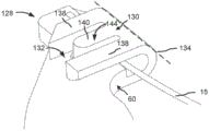
As shown, the crimp 128 is integral with the plate 60 and includes a first portion 130 and a second portion 132. The first portion 130 is configured to fold generally along the axis 134 to crimp the first and second portions 130, 132 together. As shown in fig. 20B and 20C, when the first and second portions 130, 132 are crimped together, they hold the SMA wire 15 in place. As shown above in fig. 1A and 1B, the other end of the SMA wire 15 is coupled to the support member 12.
In this embodiment, the crimp 128 includes a recess 136. As shown in fig. 20A, a recess 136 may be etched from the second portion 132 of the plate 60. Further, the first portion 130 may include a plurality of elongated members 138, 140 that include spaces therebetween. Although three elongated members 138, 140 are shown, alternative embodiments may include more or fewer elongated members 138, 140. When the first and second portions 130, 132 are crimped together, at least one of the elongated members, such as the elongated member 140, extends into the recess 136. Although only one elongate member 140 is shown extending into the recess 136, in other embodiments other elongate members may extend into respective recesses or the same recess. Further, as shown in fig. 20B and 20C, when the first portion 130 and the second portion 132 are crimped together, the elongated member 138 may contact the top of the second portion 132. In an embodiment, the edges of the recess 136 and the edges of the elongated members 138 and 140 may be rounded so that the SMA wire 15 is less likely to be damaged when the SMA wire 15 is pressed into the recess 136 by the elongated member 140.
Because the elongated member 140 extends into the recess 136, when the first and second portions 130, 132 are crimped together, the elongated member 140 provides a force perpendicular to the longitudinal axis of the SMA wire 15. Thus, the elongated member 140 deforms the SMA wire 15 and into the recess 136. Due to this configuration, the SMA wire 15 may be held in place more firmly by the crimps 128 than if the SMA wire 15 were held in place by two flat pieces of material.
In embodiments, the elongated member 140 may include additional layers of material 142 on a bottom side 143 (not shown) and/or a top side 144 (as shown in fig. 20C) of the elongated member 140 such that the elongated member 140 extends into the recess 136 and/or such that the elongated member 140 extends further into the recess 136 than the elongated member 140 would otherwise. Thus, a flat crimping tool may be used to crimp the first and second portions 130, 132 together.
Figure 21 illustrates a base layer 60 of the mobility member 14 according to an embodiment of the present invention. As shown, the base layer 60 may be substantially planar and include an attachment structure 146. In an embodiment, two diagonal corners 148 of the plate 60 may include two attachment structures 146. Each attachment structure 146 may include a crimp, such as crimps 115 and crimps 128 shown in fig. 19 and 20A-20C, respectively. Additionally or alternatively, the attachment structure 146 of the plate 60 may include one or more recesses, such as an array of multiple recesses, one or more etched patterns, and/or an array of partially etched patterns. The one or more recesses included in the attachment structure 146 may hold the SMA wire 15 more securely than if the SMA wire 15 were held in place by two pieces of flat material. The etch pattern may be formed using one or more of the etch methods described above with respect to fig. 8-14. In an embodiment, a dielectric layer and a conductive layer may be disposed on the etching pattern. After the etch pattern is made, the corners of the partial etch pattern may be rounded to reduce the likelihood of damage to the SMA wire 15.
Fig. 22A-24B illustrate an embodiment of a partial etch pattern that may be etched into the attachment structure 146. In each of the embodiments shown in fig. 22A-24B, the SMA wire 15 secured to the attachment structure 146 may be deformed by a partial etching pattern. Thus, the SMA wire 15 may be held in place more securely by the attachment structure 146 than if the SMA wire 15 were held in place by two flat pieces of material.
As an example, as shown in fig. 22A to 22B, the partial etching pattern 150 may be a staggered linear recess. In an embodiment, the partially etched patterns 150 may be offset relative to each other, for example, in an interwoven, interleaved, staggered, and/or the like relationship when the crimps included in the attachment structure 146 are crimped. As another example, as shown in fig. 23A to 23B, the partial etching pattern 152 may be an array of concave portions. As yet another example, as shown in fig. 24A to 24B, the partial etching pattern 154 may be a parallel zigzag (zig-zag).
Fig. 25A-25C illustrate another attachment structure 160 that can be incorporated into the mobility member 14 according to an embodiment of the present invention. In embodiments, the features of the attachment structure 160 discussed below may be incorporated into other attachment structures discussed herein. As shown, the attachment structure 160 includes two crimps 162. The crimp 162 is integral with the plate 60 and includes a first portion 164 and a second portion 166. First portion 164 is configured to fold generally along axis 168 to crimp first portion 164 and second portion 166 together. When the first and second portions 164, 166 are crimped together, they are able to hold the SMA wire 15 in place. As shown above in fig. 1A and 1B, the other end of the SMA wire 15 is coupled to the support member 12.
As shown, the first portion 164 includes a recess 170 and the second portion 166 includes an elongated member 172. When the first and second portions 164, 166 are crimped together, the elongated member 172 extends into the recess 170. When the first and second portions 164, 166 are crimped together, the elongated member 172 deforms the SMA wire 15 and into the recess 170. Due to this configuration, the SMA wire 15 may be held in place more firmly by the crimps 162 than if the SMA wire 15 were held in place by two flat pieces of material. In an embodiment, as shown in fig. 25B and 25C, the edge 176 may include a portion 177 that extends beyond the edge 174 such that the first portion 164 is mated to the second portion 166 when the first portion 164 and the second portion 166 are crimped together.
Further, first portion 164 includes an edge 174, and second portion 166 includes an edge 176 that is offset relative to edge 174. When the first and second portions 164, 166 are crimped together, the edges 174, 176 are configured to form cutting edges capable of severing the SMA wire 15. Fig. 25B shows the attachment structure 160 with both crimps 162 closed, and fig. 25C shows the attachment structure 160 after the edges 174 and 176 cut the end portion of the SMA wire 15.
Fig. 26A-26B illustrate another embodiment of a crimp 178 in accordance with an embodiment of the present invention. Similar to the crimps described above, the crimps 178 may be incorporated into the movable member 14 and/or the attachment structures described above. The crimp 178 is integral with the plate 60 and includes a first portion 180 and a second portion 182 configured to fold together. As shown in fig. 26B, when the first and second portions 180, 182 are folded together, they are able to crimp the SMA wire 15 in place.
As shown, the crimp 178 includes an etched recess 184. The recess 184 is generally located at a bend 186 of the crimp 178 when the first and second portions 180, 182 are crimped together. Also, the recess 184 is located on an outer portion of the bend 186. The recess 184 may reduce stress on the bend 186, which may reduce the likelihood of the plate 60 cracking when the first and second portions 180, 182 are crimped together. In embodiments, this may be advantageous when the plate 60 is made of a thicker metal and/or when the plate 60 is made of a metal having a lower plasticity (ductility) and/or a lower ductility. In an embodiment, the recess 184 may be formed by etching, such as the etching methods described above with respect to fig. 8-14.
In an embodiment, an etched recess similar to the etched recess 184 may be included in the support member 12. That is, the etched recess may be located, for example, substantially at the bend of the crimp 92a and the crimp 92b when the first portions 94a and 94b and the second portions 96a and 96b are crimped together.
Fig. 27A to 27C show another embodiment of the crimping portion 187 according to the embodiment of the invention. Similar to the crimps described above, the crimps 187 may be incorporated into the support member 12, the movable member 14, and/or the attachment structures shown above with respect to the support member 12 and the movable member 14, respectively. The crimp 187 is integral with the plate 60 and includes a first section 188 and a second section 190 configured to fold together. As shown, when the first and second portions 164, 166 are folded together, they are able to crimp the SMA wire 15 in place.
The crimp 187 includes a strain relief member 192 extending from at least one side of the crimp 187 and supporting the SMA wire 15 and/or providing a compressive force on the SMA wire 15. As shown, strain relief members 192 extend from both sides of crimp 187; however, in other embodiments, the strain relief member 192 extends from only one side of the crimp 187.
In conventional embodiments, when the suspension assembly 10 is stressed, the SMA wire 15 may be damaged and/or broken in the area adjacent to the side of the SMA wire exiting the crimp, since the area of the side of the SMA wire exiting the crimp is an inherently high stress area. When the suspension assembly 10 is stressed, the strain relief member 192 reduces the stress on the SMA wire 15, thereby increasing the bend radius of the SMA wire 15, as the strain relief member 192 can bend with the SMA wire 15. That is, instead of, for example, a length of SMA wire 15 having a width x that may be bent at an angle θ, the strain relief member 192 may increase the width of the length bent at the angle θ to, for example, 2 x, 3 x, 4 x, etc. This distributes the stress on the SMA wire 15 over a larger portion of the SMA wire 15. In embodiments, the distance that the strain relief member 192 protrudes from the side of the crimp 187 may vary depending on the type, stiffness, and/or thickness of the material used for the SMA wire 15.
In an embodiment, the strain relief member 192 may be made of metal. For example, the strain relief member 192 may be made of the same material as the trace 18, such as copper, copper alloys, or other conductors. Thus, the strain relief member 192 may be coupled to the trace 18. In an embodiment, an insulating cover layer may be applied over all or a portion of the strain relief layer 192. A corrosion-resistant metal such as gold (Au) and/or nickel (Ni) may be plated or otherwise applied over portions of the strain relief layer 192 to provide corrosion resistance. Additionally or alternatively, the strain relief member 192 may be made of a dielectric. For example, the strain relief member 192 may be made of the same material as the dielectric 78. Examples of dielectrics may include polyimide or other insulating materials. Additionally or alternatively, as shown in fig. 27B and 27C, the strain relief member 192 may include a metal pad 194 on the strain relief interior. In an embodiment, the metal pads 194 may help grip the SMA wire 15 and reduce the likelihood of the SMA wire 15 slipping out of the strain relief member 192.
Fig. 28A to 28B show another embodiment of the crimping part 196 according to an embodiment of the present invention. Similar to the crimps described above, the crimps 196 may be bonded to the support member 12, the movable member 14, and/or the attachment structures shown above with respect to the support member 12 and the movable member 14, respectively. The crimp 196 comprises two parts: a first portion 198 and a second portion 200 configured to be folded together. When the first and second portions 198, 200 are folded together, they are able to crimp the SMA wire 15 in place. One or more of the above embodiments may be incorporated into the crimp 196 to increase the holding strength of the crimp 196 and/or reduce the strain on the SMA wire 15 when the support member 10 is stressed.
The second portion 200 may be integral with the plate 60. The first portion 198 is not integral with the second portion 200, but may be coupled to the second portion 200 with an adhesive, a weld joint, and/or the like. The first and second portions 198, 200 may be coupled together on either side of the SMA wire 15. That is, in embodiments, the first and second portions 198, 200 may be coupled on an inner side 202 of the crimp 196 or an outer side 204 of the crimp.
Figure 29 illustrates a base layer 60 of the mobility member 14 according to an embodiment of the present invention. As shown, the base layer 60 may be substantially planar and include an attachment structure 206. In an embodiment, two diagonal corners 208 of the plate 60 may include two attachment structures 206. Each attachment structure 206 may include a crimp 210 such as the crimp 196 shown in fig. 28A-28B. For example, the crimp 210 included in the attachment structure 206 may include a first portion 212 that is not integral with a second portion 214 but is coupled to the second portion 214 with an adhesive, a weld joint, and/or the like. Additionally or alternatively, the attachment structure 206 of the plate 60 may include an etched pattern. The etched pattern included in the attachment structure 206 may hold the SMA wire 15 more securely than if the SMA wire 15 were held in place by two flat pieces of material. The etch pattern may be formed using one or more of the etch methods described above with respect to fig. 8-14. In an embodiment, a dielectric layer and a conductive layer may be disposed on the etching pattern. After the etch pattern is made, the corners of the partial etch pattern may be rounded to reduce the likelihood of damage to the SMA wire 15.
Although embodiments of the present invention have been described with reference to preferred embodiments, workers skilled in the art will recognize that changes may be made in form and detail without departing from the spirit and scope of the invention. For example, while the illustrated embodiment includes traces on the side of the flexure arms opposite the support member (i.e., on the top side of the traces), other embodiments can alternatively or additionally include traces on the side of the flexure arms facing the active member (i.e., on the bottom side of the traces).
Claims (50)
1. A suspension assembly comprising:
a support member comprising a metal base layer, wherein the metal base layer comprises a first attachment structure comprising:
a first portion comprising a first conductive trace separating a first space and a dielectric between the base layer and the first conductive trace; and
a second portion configured to be crimped together with the first portion, the second portion comprising a second conductive trace spaced apart by a second space and a dielectric between the base layer and the second conductive trace, wherein the first space is substantially aligned with the second conductive trace and the first conductive trace is substantially aligned with the second space; and
a movable member movably coupled to the support member, the movable member comprising a plate, wherein the plate comprises a second attachment structure; and
a shape memory alloy wire coupled to the first and second portions and the second attachment structure.
2. The suspension assembly of claim 1, wherein the metal substrate is a monolithic metal substrate.
3. The suspension assembly of claim 1, wherein the first and second portions are integral with the metal base.
4. The suspension assembly of claim 3, wherein the metal base includes a partially etched recess on an outer portion of a bend of the first and second portions when the first and second portions are crimped together.
5. The suspension assembly of claim 1, wherein the first and second portions are non-monolithic and are coupled together with at least one of an adhesive, a weld, and a weld joint.
6. The suspension assembly of claim 1, further comprising a member extending from at least one side of the first and second portions when the first and second portions are crimped together.
7. The suspension assembly of claim 6, wherein the member is integral with the dielectric.
8. A suspension assembly comprising:
a support member comprising a metal base layer, wherein the metal base layer comprises a first attachment structure;
a movable member movably coupled to the support member, the movable member comprising a plate, wherein the plate comprises a second attachment structure comprising:
a first portion comprising first elongate features separating a first space; and
a second portion configured to be crimped together with the first portion, the second portion including second elongated features spaced apart by a second space, wherein the first space is substantially aligned with the second elongated features and the first elongated features are substantially aligned with the second space; and
a shape memory alloy wire coupled to the first attachment structure and the first and second portions.
9. The suspension assembly of claim 8, wherein the first and second elongated features are formed of an electrically conductive material.
10. The suspension assembly of claim 8, wherein the first and second elongated features are formed of a dielectric.
11. The suspension assembly of claim 10, further comprising: a first electrically conductive layer disposed over the first elongated feature and the first space and a second electrically conductive layer disposed over the second elongated feature and the second space.
12. The suspension assembly of claim 11, wherein the first and second conductive layers are electrically coupled to the plate.
13. The suspension assembly of claim 11, wherein the first and second conductive layers are continuous conductive layers.
14. The suspension assembly of claim 8, wherein the first portion includes an etched recess that receives the first elongated feature and the second portion includes an etched recess that receives the second elongated feature.
15. The suspension assembly of claim 14, wherein the etched recess includes a rounded edge.
16. The suspension assembly of claim 8, further comprising a member extending from at least one side of the first and second portions, wherein the shape memory alloy wire is crimped by the member.
17. The suspension assembly of claim 8, wherein the first and second portions are integral with the plate.
18. The suspension assembly of claim 17, wherein the plate includes a partially etched recess on an outer portion of the bend of the first and second portions when the first and second portions are crimped together.
19. The suspension assembly of claim 8, wherein the first and second portions are non-monolithic and are coupled together with at least one of an adhesive, a weld, and a weld joint.
20. The suspension assembly of claim 8, further comprising a shape alloy wire cutting pad disposed on the plate.
21. A suspension assembly comprising:
a support member comprising a metal base layer, wherein the base layer comprises a first attachment structure;
a movable member movably coupled to the support member, the movable member comprising a plate, wherein the plate comprises a second attachment structure comprising:
a first portion; and
a second portion configured to be crimped together with the first portion, wherein at least one of the first portion and the second portion comprises at least one etched recess; and
a shape memory alloy wire coupled to the first attachment structure and the first and second portions.
22. The suspension assembly of claim 21, wherein the first and second portions each include at least one etched recess.
23. The suspension assembly of claim 21, further comprising: a conductive layer disposed on the first portion and the second portion.
24. The suspension assembly of claim 21, wherein the first and second portions are non-monolithic and are coupled together with at least one of an adhesive, a weld, and a weld joint.
25. The suspension assembly of claim 21, further comprising a member extending from at least one side of the first and second portions, wherein the shape memory alloy wire is crimped by the member.
26. The suspension assembly of claim 21, further comprising a shape alloy wire cutting pad disposed on the plate.
27. The suspension assembly of claim 21, wherein the etched recess comprises an array of a plurality of recesses.
28. The suspension assembly of claim 27, wherein the plurality of recesses comprises at least one of the following patterns: an array of recesses, parallel saw-tooth shaped, parallel linear recesses.
29. A suspension assembly comprising:
a support member, the support member comprising: a metal base layer, wherein the base layer comprises a first attachment structure comprising:
a first portion comprising a recess, a land, and a first edge between the recess and the land; and
a second portion configured to be crimped together with the first portion, the second portion including a second edge offset relative to the first edge, the first and second edges forming a cutting edge when the first and second portions are crimped together;
a movable member movably coupled to the support member, the movable member comprising a plate, wherein the plate comprises a second attachment structure; and
a shape memory alloy wire coupled to the second attachment structure and the first and second portions.
30. The suspension assembly of claim 29, further comprising: a conductive layer disposed on the first portion and the second portion.
31. The suspension assembly of claim 29, wherein the first and second portions are non-monolithic and are coupled together with at least one of an adhesive, a weld, and a weld joint.
32. The suspension assembly of claim 29, further comprising a member extending from at least one side of the first and second portions, wherein the shape memory alloy wire is crimped by the member.
33. A suspension assembly comprising:
a support member comprising a metal base layer, wherein the base layer comprises a first attachment structure;
a movable member movably coupled to the support member, the movable member comprising a plate, wherein the plate comprises a second attachment structure comprising:
a first portion;
a second portion configured to be crimped together with the first portion; and
a member extending from at least one side of the first and second portions when the first and second portions are crimped together; and
a shape memory alloy wire coupled to the first attachment structure, the first and second portions, and a mechanical engagement member.
34. The suspension assembly of claim 33, wherein the first and second portions include etched recesses.
35. The suspension assembly of claim 33, wherein the first portion includes first dielectric features that space a first space; and the second portion includes a second dielectric feature spaced apart by a second space, wherein the first space is substantially aligned with the second dielectric feature and the first dielectric feature is substantially aligned with the second space.
36. The suspension assembly of claim 35, wherein the member extending from at least one side of the first and second portions is integral with at least one of the dielectric features.
37. The suspension assembly of claim 35, further comprising: a first conductive layer disposed over the first dielectric feature and the first space and a second conductive layer disposed over the second dielectric feature and the second space.
38. The suspension assembly of claim 37, wherein the first and second conductive layers are electrically coupled to the plate.
39. The suspension assembly of claim 37, wherein the first and second conductive layers are continuous conductive layers.
40. The suspension assembly of claim 35, wherein the first portion includes an etched recess that receives a first member and the second portion includes an etched recess that receives a second member.
41. The suspension assembly of claim 34, wherein the etched recess includes a rounded edge.
42. The suspension assembly of claim 33, wherein the first and second portions are non-monolithic and are coupled together with at least one of an adhesive, a weld, and a weld joint.
43. A suspension assembly comprising:
a support member comprising a metal base layer, wherein the base layer comprises a first attachment structure;
a movable member movably coupled to the support member, the movable member comprising:
a plate comprising a first portion; and
a second portion configured to be crimped together with the first portion, wherein the second portion is not integral with the first portion and is coupled together with at least one of an adhesive, a weld, and a weld joint; and
a shape memory alloy wire coupled to the first attachment structure and the first and second portions.
44. The suspension assembly of claim 43, wherein the first and second portions include etched recesses.
45. The suspension assembly of claim 43, wherein the first portion includes first dielectric features that space a first space; and the second portion includes a second dielectric feature spaced apart by a second space, wherein the first space is substantially aligned with the second dielectric feature and the first dielectric feature is substantially aligned with the second space.
46. The suspension assembly of claim 45, further comprising: a first conductive layer disposed over the first dielectric feature and the first space and a second conductive layer disposed over the second dielectric feature and the second space.
47. The suspension assembly of claim 46, wherein the first and second conductive layers are electrically coupled to the plate.
48. The suspension assembly of claim 46, wherein the first and second conductive layers are continuous conductive layers.
49. The suspension assembly of claim 45, wherein the first portion includes an etched recess that receives the first dielectric feature and the second portion includes an etched recess that receives the second dielectric feature.
50. The suspension assembly of claim 44, wherein the etched recess includes a rounded edge.
Priority Applications (1)
| Application Number | Priority Date | Filing Date | Title |
|---|---|---|---|
| CN202010257836.5A CN111562681B (en) | 2015-03-06 | 2016-03-07 | Shape memory alloy wire attachment structure for suspension assembly |
Applications Claiming Priority (3)
| Application Number | Priority Date | Filing Date | Title |
|---|---|---|---|
| US201562129562P | 2015-03-06 | 2015-03-06 | |
| US62/129,562 | 2015-03-06 | ||
| PCT/US2016/021230 WO2016144895A1 (en) | 2015-03-06 | 2016-03-07 | Shape memory alloy wire attachment structures for a suspension assembly |
Related Child Applications (1)
| Application Number | Title | Priority Date | Filing Date |
|---|---|---|---|
| CN202010257836.5A Division CN111562681B (en) | 2015-03-06 | 2016-03-07 | Shape memory alloy wire attachment structure for suspension assembly |
Publications (2)
| Publication Number | Publication Date |
|---|---|
| CN107532574A CN107532574A (en) | 2018-01-02 |
| CN107532574B true CN107532574B (en) | 2020-05-05 |
Family
ID=56849866
Family Applications (2)
| Application Number | Title | Priority Date | Filing Date |
|---|---|---|---|
| CN201680025323.3A Active CN107532574B (en) | 2015-03-06 | 2016-03-07 | Shape memory alloy wire attachment structure for suspension assembly |
| CN202010257836.5A Active CN111562681B (en) | 2015-03-06 | 2016-03-07 | Shape memory alloy wire attachment structure for suspension assembly |
Family Applications After (1)
| Application Number | Title | Priority Date | Filing Date |
|---|---|---|---|
| CN202010257836.5A Active CN111562681B (en) | 2015-03-06 | 2016-03-07 | Shape memory alloy wire attachment structure for suspension assembly |
Country Status (6)
| Country | Link |
|---|---|
| US (3) | US9454016B1 (en) |
| EP (1) | EP3265678B1 (en) |
| JP (2) | JP7185400B2 (en) |
| KR (1) | KR102619009B1 (en) |
| CN (2) | CN107532574B (en) |
| WO (1) | WO2016144895A1 (en) |
Families Citing this family (30)
| Publication number | Priority date | Publication date | Assignee | Title |
|---|---|---|---|---|
| GB201412848D0 (en) | 2014-07-18 | 2014-09-03 | Cambridge Mechatronics Ltd | Suspension system for a camera lens element |
| US9366879B1 (en) | 2014-12-02 | 2016-06-14 | Hutchinson Technology Incorporated | Camera lens suspension with polymer bearings |
| US9454016B1 (en) * | 2015-03-06 | 2016-09-27 | Hutchinson Technology Incorporated | Camera lens suspension with integrated electrical leads |
| US10670878B2 (en) | 2016-05-19 | 2020-06-02 | Hutchinson Technology Incorporated | Camera lens suspensions |
| KR20190015528A (en) | 2016-06-09 | 2019-02-13 | 허친슨 테크놀로지 인코포레이티드 | Shape memory alloy wire attachment structure having an adhesive for a suspension assembly |
| CN110199119B (en) * | 2016-12-16 | 2022-11-18 | 哈钦森技术股份有限公司 | Suspension assembly |
| US11199182B2 (en) | 2016-12-16 | 2021-12-14 | Hutchinson Technology Incorporated | Sensor shift structures in optical image stabilization suspensions |
| EP3982196A1 (en) * | 2017-04-06 | 2022-04-13 | LG Innotek Co., Ltd. | Lens driving unit, and camera module and optical apparatus including same |
| KR102400118B1 (en) * | 2017-08-14 | 2022-05-19 | 엘지이노텍 주식회사 | A lens moving unit, and camera module and optical instrument including the same |
| GB201707542D0 (en) * | 2017-05-11 | 2017-06-28 | Cambridge Mechatronics Ltd | Compact SMA shutter actuator |
| US11231022B2 (en) * | 2017-05-17 | 2022-01-25 | Cambridge Mechatronics Limited | Electrical connections for SMA actuators |
| CN109212710B (en) * | 2017-06-29 | 2021-01-15 | 台湾东电化股份有限公司 | Lens driving system and circuit module thereof |
| KR102148513B1 (en) | 2017-09-28 | 2020-08-26 | 주식회사 엘지화학 | A carbon -surfur complex, manufacturing method thereof and lithium secondary battery comprising the same |
| US10634929B2 (en) * | 2017-10-19 | 2020-04-28 | Tdk Taiwan Corp. | Optical driving mechanism |
| CN108247309B (en) * | 2017-12-20 | 2020-05-22 | 东莞市亚登电子有限公司 | Memory alloy wire mounting method for micro optical camera module |
| CN108111724B (en) * | 2017-12-20 | 2020-05-19 | 东莞市亚登电子有限公司 | Memory alloy wire implantation method for micro optical camera module |
| US11454221B2 (en) * | 2018-01-22 | 2022-09-27 | Cambridge Mechatronics Limited | Shape memory alloy actuation apparatus |
| US11019266B1 (en) | 2018-08-31 | 2021-05-25 | Apple Inc. | Blunting optical suspension springs for particle reduction |
| JP2020056379A (en) * | 2018-10-03 | 2020-04-09 | フォスター電機株式会社 | Actuator |
| US11226466B2 (en) * | 2019-02-01 | 2022-01-18 | Tdk Taiwan Corp. | Optical element driving mechanism |
| WO2020243861A1 (en) * | 2019-06-01 | 2020-12-10 | 瑞声光学解决方案私人有限公司 | Automatic focusing lens assembly |
| US11503211B2 (en) | 2019-08-16 | 2022-11-15 | Hutchinson Technology Incorporated | Stabilization suspensions and methods of manufacture |
| GB2587906A (en) * | 2019-08-16 | 2021-04-14 | Hutchinson Technology | Stabilization suspensions and methods of manufacture |
| CN110703404A (en) * | 2019-09-11 | 2020-01-17 | 瑞声科技(新加坡)有限公司 | Lens module |
| CN112698462A (en) | 2019-10-18 | 2021-04-23 | 新思考电机有限公司 | Optical member driving device, camera device, and electronic apparatus |
| CN212211175U (en) * | 2020-06-23 | 2020-12-22 | 新思考电机有限公司 | OIS motor drive structure, OIS motor, camera device |
| US11582389B2 (en) * | 2020-08-11 | 2023-02-14 | Apple Inc. | Electrical traces in suspension assemblies |
| JP2022038456A (en) * | 2020-08-26 | 2022-03-10 | アルプスアルパイン株式会社 | Lens drive device and camera module |
| US11194115B1 (en) | 2020-09-02 | 2021-12-07 | Hutchinson Technology Incorporated | Guided autofocus assembly |
| GB2607269A (en) * | 2021-04-14 | 2022-12-07 | Cambridge Mechatronics Ltd | SMA actuator assembly |
Citations (4)
| Publication number | Priority date | Publication date | Assignee | Title |
|---|---|---|---|---|
| EP1870962A2 (en) * | 2006-06-22 | 2007-12-26 | Autosplice, Inc. | Apparatus and methods for filament crimping and manufacturing of crimp element assemblies |
| CN101668947A (en) * | 2007-02-12 | 2010-03-10 | 剑桥机电有限公司 | Shape memory alloy actuation apparatus |
| CN101876742A (en) * | 2009-04-28 | 2010-11-03 | 三美电机株式会社 | Lens driver |
| CN102089695A (en) * | 2008-07-11 | 2011-06-08 | 精工电子有限公司 | Drive module, method of assembling the same, and electronic apparatus |
Family Cites Families (111)
| Publication number | Priority date | Publication date | Assignee | Title |
|---|---|---|---|---|
| CH457131A (en) | 1967-09-06 | 1968-05-31 | Koch Carl | Photographic focusing screen camera |
| US3776447A (en) | 1969-06-30 | 1973-12-04 | Texas Instruments Inc | Automatic semiconductor bonding machine |
| US3734386A (en) | 1971-06-30 | 1973-05-22 | Ibm | Wiring apparatus with wire path forming means |
| US4140265A (en) | 1975-06-26 | 1979-02-20 | Kollmorgen Technologies Corporation | Method and apparatus for positioning the end of a conductive filament at a predetermined and repeatable geometric location for coupling to a predetermined terminal area of an element |
| JPS5698900A (en) | 1980-01-07 | 1981-08-08 | Hitachi Ltd | Device for automatically wiring printed circuit board |
| JPS57201739U (en) | 1981-06-19 | 1982-12-22 | ||
| JPS59104565U (en) | 1982-12-29 | 1984-07-13 | 日本メクトロン株式会社 | flexible circuit board |
| EP0203597B1 (en) | 1985-05-31 | 1990-07-11 | Emhart Industries, Inc. | Bonding head |
| US5743654A (en) | 1987-05-29 | 1998-04-28 | Kmc, Inc. | Hydrostatic and active control movable pad bearing |
| JPS6473754A (en) | 1987-09-16 | 1989-03-20 | Nec Corp | Manufacture of lead frame for semiconductor device |
| JPH01186577A (en) | 1988-01-13 | 1989-07-26 | Shin Nippon Koki Kk | Connector connection tool |
| US4984581A (en) | 1988-10-12 | 1991-01-15 | Flexmedics Corporation | Flexible guide having two-way shape memory alloy |
| JPH0358464A (en) | 1989-07-26 | 1991-03-13 | Nec Corp | Semiconductor device |
| JPH05283146A (en) | 1992-03-31 | 1993-10-29 | Toshiba Lighting & Technol Corp | Thick-film resistance heating element |
| US5269810A (en) | 1992-06-19 | 1993-12-14 | W. L. Gore & Associates, Inc. | Patch electrode |
| JP2959322B2 (en) | 1993-03-09 | 1999-10-06 | 住友電装株式会社 | Harness electric wire manufacturing apparatus and manufacturing method |
| JPH06275325A (en) | 1993-03-24 | 1994-09-30 | Mitsubishi Electric Home Appliance Co Ltd | Connecting structure for conducting wire |
| US5667884A (en) | 1993-04-12 | 1997-09-16 | Bolger; Justin C. | Area bonding conductive adhesive preforms |
| JPH07259725A (en) | 1994-03-17 | 1995-10-09 | Olympus Optical Co Ltd | Flexible tube curing device |
| JP2955829B2 (en) * | 1994-04-15 | 1999-10-04 | ハッチンソン テクノロジー インコーポレイテッド | Head suspension |
| DE19549174A1 (en) * | 1995-10-28 | 1997-07-03 | Bosch Gmbh Robert | Contact element with crimp section |
| US5831820A (en) | 1996-12-30 | 1998-11-03 | Huang; James | Peripheral docking module using a shape memory alloy actuator wire |
| US6149742A (en) | 1998-05-26 | 2000-11-21 | Lockheed Martin Corporation | Process for conditioning shape memory alloys |
| JP3488100B2 (en) | 1998-10-13 | 2004-01-19 | 矢崎総業株式会社 | Automatic cutting and crimping equipment |
| KR20020021809A (en) | 1999-08-12 | 2002-03-22 | 추후기재 | Shape-memory alloy actuators and control methods |
| US6639411B1 (en) | 2000-09-05 | 2003-10-28 | Hutchinson Technology Incorporated | Microactuated suspension motor failure detection system |
| JP2002130114A (en) | 2000-10-20 | 2002-05-09 | Toshiba Corp | Actuator device |
| EP1364125A1 (en) | 2001-01-17 | 2003-11-26 | M 2 Medical A/S | Shape memory alloy actuator |
| JP4406707B2 (en) | 2001-06-06 | 2010-02-03 | ソニー株式会社 | Two-axis device for optical disk device |
| JP4278364B2 (en) | 2002-11-08 | 2009-06-10 | パイオニア株式会社 | Actuator for pickup device |
| US6916115B1 (en) | 2003-03-04 | 2005-07-12 | University Of Kentucky Research Foundation | System and device for characterizing shape memory alloy wires |
| WO2005076069A1 (en) | 2004-02-06 | 2005-08-18 | Koninklijke Philips Electronics N.V. | Camera arrangement, mobile phone comprising a camera arrangement, method of manufacturing a camera arrangement |
| JP2005227365A (en) | 2004-02-10 | 2005-08-25 | Sony Corp | Method for manufacturing optical component |
| US7384531B1 (en) | 2004-02-19 | 2008-06-10 | Hutchinson Technology Incorporated | Plated ground features for integrated lead suspensions |
| JP2007537562A (en) | 2004-05-14 | 2007-12-20 | ハッチンソン テクノロジー インコーポレーティッド | Method for producing noble metal conductive lead for suspension assembly |
| US7679647B2 (en) | 2004-07-21 | 2010-03-16 | Hewlett-Packard Development Company, L.P. | Flexible suspension for image stabilization |
| CN1843058B (en) | 2004-08-12 | 2012-07-04 | 株式会社村田制作所 | Piezoelectric electroacoustic transducer |
| JP4186907B2 (en) | 2004-10-14 | 2008-11-26 | ソニー株式会社 | Electronics |
| JP2007092556A (en) | 2005-09-27 | 2007-04-12 | Konica Minolta Opto Inc | Drive device and its manufacturing method |
| US7777782B2 (en) | 2005-11-04 | 2010-08-17 | Nokia Corporation | Stabilization of an image produced by optics |
| JP4737756B2 (en) | 2006-02-27 | 2011-08-03 | Necトーキン株式会社 | Solid electrolytic capacitor |
| GB0606425D0 (en) | 2006-03-30 | 2006-05-10 | 1 Ltd | Camera lens actuation apparatus |
| EP2372428B1 (en) | 2006-03-30 | 2012-10-10 | Cambridge Mechatronics Limited | Camera lens actuation apparatus |
| US8175449B2 (en) | 2006-05-30 | 2012-05-08 | Konica Minolta Opto, Inc. | Driving device, driving mechanism, and image sensing apparatus |
| US7832082B1 (en) | 2006-10-10 | 2010-11-16 | Hutchinson Technology Incorporated | Method for manufacturing an integrated lead suspension component |
| US7929252B1 (en) | 2006-10-10 | 2011-04-19 | Hutchinson Technology Incorporated | Multi-layer ground plane structures for integrated lead suspensions |
| JP4816397B2 (en) | 2006-10-12 | 2011-11-16 | 住友電気工業株式会社 | Photoelectric conversion module |
| AU2008210504B2 (en) | 2007-01-29 | 2012-07-26 | Spinal Modulation, Inc. | Sutureless lead retention features |
| GB2457860B (en) | 2007-02-12 | 2010-06-30 | Cambridge Mechatronics Ltd | Shape memory alloy actuation apparatus |
| GB0702835D0 (en) | 2007-02-14 | 2007-03-28 | Johnson Electric Sa | Lens module |
| JP2008233526A (en) | 2007-03-20 | 2008-10-02 | Tamron Co Ltd | Actuator for preventing image shake and camera equipped therewith |
| US7974025B2 (en) | 2007-04-23 | 2011-07-05 | Cambridge Mechatronics Limited | Shape memory alloy actuation apparatus |
| EP2140138B1 (en) | 2007-04-23 | 2012-04-11 | Cambridge Mechatronics Limited | Shape memory alloy actuation apparatus |
| JP5194622B2 (en) | 2007-08-02 | 2013-05-08 | コニカミノルタアドバンストレイヤー株式会社 | Drive mechanism, drive device, and lens drive device |
| CN101408655B (en) | 2007-10-11 | 2011-07-27 | 鸿富锦精密工业(深圳)有限公司 | Lens module |
| JP5101984B2 (en) | 2007-10-23 | 2012-12-19 | セイコーインスツル株式会社 | Drive module |
| JP4355742B2 (en) | 2007-10-31 | 2009-11-04 | 三菱電機エンジニアリング株式会社 | Short-circuit plate |
| KR20090081855A (en) | 2008-01-25 | 2009-07-29 | 이-핀 옵티칼 인더스트리 컴퍼니 리미티드 | Lens displacement mechanism using shaped memory alloy |
| US8388773B2 (en) | 2008-03-07 | 2013-03-05 | GM Global Technology Operations LLC | Apparatus for and method of conditioning shape memory alloy wire |
| US8169746B1 (en) | 2008-04-08 | 2012-05-01 | Hutchinson Technology Incorporated | Integrated lead suspension with multiple trace configurations |
| GB2481146B (en) * | 2008-07-30 | 2012-05-23 | Cambridge Mechatronics Ltd | Shape memory alloy actuation apparatus |
| JP5458101B2 (en) | 2008-09-12 | 2014-04-02 | ケンブリッジ メカトロニクス リミテッド | Optical image stabilization |
| JP2010128262A (en) | 2008-11-28 | 2010-06-10 | Mitsumi Electric Co Ltd | Lens drive unit and connection method |
| WO2010089526A2 (en) | 2009-02-09 | 2010-08-12 | Cambridge Mechatronics Limited | Shape memory alloy actuation apparatus |
| US8570384B2 (en) | 2009-02-09 | 2013-10-29 | Cambridge Mechatronics Limited | Camera apparatus having an SMA actuator system |
| JP2010192036A (en) | 2009-02-18 | 2010-09-02 | Funai Electric Co Ltd | Objective lens actuator |
| CN102356508B (en) | 2009-03-16 | 2016-04-13 | 永备电池有限公司 | There is the oxygen consumption battery pack of the high rate capability of improvement |
| WO2010110122A1 (en) | 2009-03-25 | 2010-09-30 | コニカミノルタオプト株式会社 | Actuator, drive device, and imaging device |
| JP2011039485A (en) | 2009-07-14 | 2011-02-24 | Seiko Instruments Inc | Drive module and electronic device |
| JP4804564B2 (en) | 2009-07-14 | 2011-11-02 | キヤノン株式会社 | Optical apparatus having shake correction device |
| JP5846346B2 (en) | 2009-08-21 | 2016-01-20 | ミツミ電機株式会社 | Camera shake correction device |
| JP2011107413A (en) | 2009-11-17 | 2011-06-02 | Morioka Seiko Instruments Inc | Actuator, drive module, and electronic equipment |
| JP2011175160A (en) | 2010-02-25 | 2011-09-08 | Mitsumi Electric Co Ltd | Lens driving device |
| WO2011104518A1 (en) | 2010-02-26 | 2011-09-01 | Cambridge Mechatronics Limited | Sma actuation apparatus |
| US9999763B2 (en) | 2012-06-13 | 2018-06-19 | Mainstay Medical Limited | Apparatus and methods for anchoring electrode leads adjacent to nervous tissue |
| US8885299B1 (en) | 2010-05-24 | 2014-11-11 | Hutchinson Technology Incorporated | Low resistance ground joints for dual stage actuation disk drive suspensions |
| JP2012032470A (en) | 2010-07-29 | 2012-02-16 | Sony Corp | Lens module and camera |
| KR101893229B1 (en) * | 2010-08-09 | 2018-08-29 | 캠브리지 메카트로닉스 리미티드 | Camera apparatus |
| WO2012038703A2 (en) | 2010-09-22 | 2012-03-29 | Cambridge Mechatronics Limited | Optical image stabilisation |
| GB201019532D0 (en) | 2010-11-18 | 2010-12-29 | Cambridge Mechatronics Ltd | Optical image stablisation drive |
| WO2012071003A1 (en) | 2010-11-22 | 2012-05-31 | Senseair Ab | Method for the wafer-level integration of shape memory alloy wires |
| US8851443B2 (en) | 2010-12-15 | 2014-10-07 | Autosplice, Inc. | Memory alloy-actuated apparatus and methods for making and using the same |
| JP5821356B2 (en) | 2011-07-15 | 2015-11-24 | ミツミ電機株式会社 | Lens drive device |
| DE102012113093A1 (en) | 2011-12-29 | 2013-07-04 | Johnson Electric S.A. | storekeeper |
| JP2013178457A (en) | 2012-02-01 | 2013-09-09 | Seiko Instruments Inc | Drive module and electronic apparatus |
| US9288394B2 (en) | 2012-02-01 | 2016-03-15 | Ricoh Imaging Company, Ltd. | Stage apparatus and camera shake correction apparatus |
| CN104204935B (en) | 2012-02-16 | 2017-05-10 | 剑桥机电有限公司 | shape memory alloy actuation apparatus |
| KR20130098635A (en) | 2012-02-28 | 2013-09-05 | 삼성전자주식회사 | Capillary exchange system of semiconductor wire bond |
| GB201206490D0 (en) | 2012-04-12 | 2012-05-30 | Cambridge Mechatronics Ltd | Compact camera |
| JP2013238848A (en) | 2012-04-20 | 2013-11-28 | Hoya Corp | Imaging apparatus |
| CN104335101B (en) | 2012-05-25 | 2017-04-19 | 剑桥机电有限公司 | shape memory alloy actuation apparatus |
| JP5967366B2 (en) | 2012-09-11 | 2016-08-10 | Smk株式会社 | Flat shape memory cable body and driving device using the same |
| GB201220485D0 (en) | 2012-11-14 | 2012-12-26 | Cambridge Mechatronics Ltd | Control of an SMA actuation apparatus |
| GB201221306D0 (en) | 2012-11-27 | 2013-01-09 | Cambridge Mechatronics Ltd | Suspension system for a camera lens element |
| WO2014100516A1 (en) | 2012-12-20 | 2014-06-26 | Bynlac Laboratories Llc | Voice coil motor optical image stabilization |
| JP2014225378A (en) | 2013-05-16 | 2014-12-04 | 株式会社日立製作所 | Sealant for tab lead, tab lead and lithium ion secondary battery |
| KR101569345B1 (en) | 2013-07-25 | 2015-11-16 | 크루셜텍 (주) | Actuator Using Shape Memory Alloy Wire |
| US9277789B2 (en) * | 2013-09-10 | 2016-03-08 | Texas Instruments Incorporated | Current, temperature or electromagnetic field actuated fasteners |
| WO2015036761A1 (en) | 2013-09-12 | 2015-03-19 | Cambridge Mechatronics Limited | Insulation of sma actuator wires in a miniature camera |
| JP2015128267A (en) | 2013-12-27 | 2015-07-09 | セイコーエプソン株式会社 | Vibration piece, vibrator, oscillator, electronic apparatus, sensor and movable body |
| GB201403803D0 (en) | 2014-03-04 | 2014-04-16 | Cambridge Mechatronics Ltd | SMA actuator |
| GB201412848D0 (en) | 2014-07-18 | 2014-09-03 | Cambridge Mechatronics Ltd | Suspension system for a camera lens element |
| US9366879B1 (en) | 2014-12-02 | 2016-06-14 | Hutchinson Technology Incorporated | Camera lens suspension with polymer bearings |
| US9454016B1 (en) | 2015-03-06 | 2016-09-27 | Hutchinson Technology Incorporated | Camera lens suspension with integrated electrical leads |
| JP6447819B2 (en) | 2015-03-10 | 2019-01-09 | セイコーエプソン株式会社 | Head and liquid ejecting apparatus |
| EP3278354B1 (en) | 2015-04-02 | 2024-03-20 | Hutchinson Technology Incorporated | Wire feeding and attaching system for camera lens suspensions |
| GB201517202D0 (en) | 2015-09-29 | 2015-11-11 | Cambridge Mechatronics Ltd | OIS actuator improvements |
| CN116055845A (en) | 2015-10-28 | 2023-05-02 | 剑桥机电有限公司 | Camera assembly providing optical image stabilization |
| US10670878B2 (en) | 2016-05-19 | 2020-06-02 | Hutchinson Technology Incorporated | Camera lens suspensions |
| KR20190015528A (en) | 2016-06-09 | 2019-02-13 | 허친슨 테크놀로지 인코포레이티드 | Shape memory alloy wire attachment structure having an adhesive for a suspension assembly |
| CN111405743B (en) | 2019-01-03 | 2023-09-05 | 新科实业有限公司 | Suspension assembly of optical image stabilizer |
-
2015
- 2015-09-23 US US14/863,046 patent/US9454016B1/en active Active
-
2016
- 2016-03-07 CN CN201680025323.3A patent/CN107532574B/en active Active
- 2016-03-07 WO PCT/US2016/021230 patent/WO2016144895A1/en active Application Filing
- 2016-03-07 KR KR1020177027642A patent/KR102619009B1/en active IP Right Grant
- 2016-03-07 US US15/063,151 patent/US11782286B2/en active Active
- 2016-03-07 EP EP16762309.9A patent/EP3265678B1/en active Active
- 2016-03-07 JP JP2017546796A patent/JP7185400B2/en active Active
- 2016-03-07 CN CN202010257836.5A patent/CN111562681B/en active Active
- 2016-09-26 US US15/276,115 patent/US10036897B2/en active Active
-
2021
- 2021-04-15 JP JP2021068927A patent/JP7200286B2/en active Active
Patent Citations (4)
| Publication number | Priority date | Publication date | Assignee | Title |
|---|---|---|---|---|
| EP1870962A2 (en) * | 2006-06-22 | 2007-12-26 | Autosplice, Inc. | Apparatus and methods for filament crimping and manufacturing of crimp element assemblies |
| CN101668947A (en) * | 2007-02-12 | 2010-03-10 | 剑桥机电有限公司 | Shape memory alloy actuation apparatus |
| CN102089695A (en) * | 2008-07-11 | 2011-06-08 | 精工电子有限公司 | Drive module, method of assembling the same, and electronic apparatus |
| CN101876742A (en) * | 2009-04-28 | 2010-11-03 | 三美电机株式会社 | Lens driver |
Also Published As
| Publication number | Publication date |
|---|---|
| US20160259177A1 (en) | 2016-09-08 |
| CN111562681B (en) | 2024-03-15 |
| KR20170125909A (en) | 2017-11-15 |
| JP7200286B2 (en) | 2023-01-06 |
| EP3265678B1 (en) | 2020-08-19 |
| US20170131562A1 (en) | 2017-05-11 |
| JP2021193443A (en) | 2021-12-23 |
| US10036897B2 (en) | 2018-07-31 |
| CN111562681A (en) | 2020-08-21 |
| EP3265678A1 (en) | 2018-01-10 |
| EP3265678A4 (en) | 2018-08-29 |
| US11782286B2 (en) | 2023-10-10 |
| JP2018514679A (en) | 2018-06-07 |
| US20160258425A1 (en) | 2016-09-08 |
| CN107532574A (en) | 2018-01-02 |
| KR102619009B1 (en) | 2023-12-29 |
| JP7185400B2 (en) | 2022-12-07 |
| WO2016144895A1 (en) | 2016-09-15 |
| US9454016B1 (en) | 2016-09-27 |
Similar Documents
| Publication | Publication Date | Title |
|---|---|---|
| CN107532574B (en) | Shape memory alloy wire attachment structure for suspension assembly | |
| CN109562592B (en) | Shape memory alloy wire attachment structure with adhesive for suspension assembly | |
| US11635631B2 (en) | Integrated camera lens suspension | |
| JP4944210B2 (en) | Communication jack with multi-layer plug interface contacts | |
| JP5826620B2 (en) | connector |
Legal Events
| Date | Code | Title | Description |
|---|---|---|---|
| PB01 | Publication | ||
| PB01 | Publication | ||
| SE01 | Entry into force of request for substantive examination | ||
| SE01 | Entry into force of request for substantive examination | ||
| GR01 | Patent grant | ||
| GR01 | Patent grant |