JP4944210B2 - Communication jack with multi-layer plug interface contacts - Google Patents
Communication jack with multi-layer plug interface contacts Download PDFInfo
- Publication number
- JP4944210B2 JP4944210B2 JP2009541588A JP2009541588A JP4944210B2 JP 4944210 B2 JP4944210 B2 JP 4944210B2 JP 2009541588 A JP2009541588 A JP 2009541588A JP 2009541588 A JP2009541588 A JP 2009541588A JP 4944210 B2 JP4944210 B2 JP 4944210B2
- Authority
- JP
- Japan
- Prior art keywords
- plug
- jack
- communication
- plug interface
- contact
- Prior art date
- Legal status (The legal status is an assumption and is not a legal conclusion. Google has not performed a legal analysis and makes no representation as to the accuracy of the status listed.)
- Expired - Fee Related
Links
Images


Classifications
-
- H—ELECTRICITY
- H01—ELECTRIC ELEMENTS
- H01R—ELECTRICALLY-CONDUCTIVE CONNECTIONS; STRUCTURAL ASSOCIATIONS OF A PLURALITY OF MUTUALLY-INSULATED ELECTRICAL CONNECTING ELEMENTS; COUPLING DEVICES; CURRENT COLLECTORS
- H01R13/00—Details of coupling devices of the kinds covered by groups H01R12/70 or H01R24/00 - H01R33/00
- H01R13/66—Structural association with built-in electrical component
- H01R13/665—Structural association with built-in electrical component with built-in electronic circuit
- H01R13/6658—Structural association with built-in electrical component with built-in electronic circuit on printed circuit board
-
- H—ELECTRICITY
- H01—ELECTRIC ELEMENTS
- H01R—ELECTRICALLY-CONDUCTIVE CONNECTIONS; STRUCTURAL ASSOCIATIONS OF A PLURALITY OF MUTUALLY-INSULATED ELECTRICAL CONNECTING ELEMENTS; COUPLING DEVICES; CURRENT COLLECTORS
- H01R13/00—Details of coupling devices of the kinds covered by groups H01R12/70 or H01R24/00 - H01R33/00
- H01R13/02—Contact members
- H01R13/04—Pins or blades for co-operation with sockets
- H01R13/08—Resiliently-mounted rigid pins or blades
-
- H—ELECTRICITY
- H01—ELECTRIC ELEMENTS
- H01R—ELECTRICALLY-CONDUCTIVE CONNECTIONS; STRUCTURAL ASSOCIATIONS OF A PLURALITY OF MUTUALLY-INSULATED ELECTRICAL CONNECTING ELEMENTS; COUPLING DEVICES; CURRENT COLLECTORS
- H01R13/00—Details of coupling devices of the kinds covered by groups H01R12/70 or H01R24/00 - H01R33/00
- H01R13/46—Bases; Cases
-
- H—ELECTRICITY
- H01—ELECTRIC ELEMENTS
- H01R—ELECTRICALLY-CONDUCTIVE CONNECTIONS; STRUCTURAL ASSOCIATIONS OF A PLURALITY OF MUTUALLY-INSULATED ELECTRICAL CONNECTING ELEMENTS; COUPLING DEVICES; CURRENT COLLECTORS
- H01R13/00—Details of coupling devices of the kinds covered by groups H01R12/70 or H01R24/00 - H01R33/00
- H01R13/646—Details of coupling devices of the kinds covered by groups H01R12/70 or H01R24/00 - H01R33/00 specially adapted for high-frequency, e.g. structures providing an impedance match or phase match
- H01R13/6461—Means for preventing cross-talk
- H01R13/6464—Means for preventing cross-talk by adding capacitive elements
-
- H—ELECTRICITY
- H01—ELECTRIC ELEMENTS
- H01R—ELECTRICALLY-CONDUCTIVE CONNECTIONS; STRUCTURAL ASSOCIATIONS OF A PLURALITY OF MUTUALLY-INSULATED ELECTRICAL CONNECTING ELEMENTS; COUPLING DEVICES; CURRENT COLLECTORS
- H01R24/00—Two-part coupling devices, or either of their cooperating parts, characterised by their overall structure
- H01R24/28—Coupling parts carrying pins, blades or analogous contacts and secured only to wire or cable
-
- H—ELECTRICITY
- H01—ELECTRIC ELEMENTS
- H01R—ELECTRICALLY-CONDUCTIVE CONNECTIONS; STRUCTURAL ASSOCIATIONS OF A PLURALITY OF MUTUALLY-INSULATED ELECTRICAL CONNECTING ELEMENTS; COUPLING DEVICES; CURRENT COLLECTORS
- H01R24/00—Two-part coupling devices, or either of their cooperating parts, characterised by their overall structure
- H01R24/60—Contacts spaced along planar side wall transverse to longitudinal axis of engagement
- H01R24/62—Sliding engagements with one side only, e.g. modular jack coupling devices
- H01R24/64—Sliding engagements with one side only, e.g. modular jack coupling devices for high frequency, e.g. RJ 45
-
- H—ELECTRICITY
- H01—ELECTRIC ELEMENTS
- H01R—ELECTRICALLY-CONDUCTIVE CONNECTIONS; STRUCTURAL ASSOCIATIONS OF A PLURALITY OF MUTUALLY-INSULATED ELECTRICAL CONNECTING ELEMENTS; COUPLING DEVICES; CURRENT COLLECTORS
- H01R2107/00—Four or more poles
-
- H—ELECTRICITY
- H05—ELECTRIC TECHNIQUES NOT OTHERWISE PROVIDED FOR
- H05K—PRINTED CIRCUITS; CASINGS OR CONSTRUCTIONAL DETAILS OF ELECTRIC APPARATUS; MANUFACTURE OF ASSEMBLAGES OF ELECTRICAL COMPONENTS
- H05K1/00—Printed circuits
- H05K1/02—Details
- H05K1/0213—Electrical arrangements not otherwise provided for
- H05K1/0216—Reduction of cross-talk, noise or electromagnetic interference
- H05K1/0228—Compensation of cross-talk by a mutually correlated lay-out of printed circuit traces, e.g. for compensation of cross-talk in mounted connectors
-
- H—ELECTRICITY
- H05—ELECTRIC TECHNIQUES NOT OTHERWISE PROVIDED FOR
- H05K—PRINTED CIRCUITS; CASINGS OR CONSTRUCTIONAL DETAILS OF ELECTRIC APPARATUS; MANUFACTURE OF ASSEMBLAGES OF ELECTRICAL COMPONENTS
- H05K1/00—Printed circuits
- H05K1/02—Details
- H05K1/14—Structural association of two or more printed circuits
- H05K1/147—Structural association of two or more printed circuits at least one of the printed circuits being bent or folded, e.g. by using a flexible printed circuit
-
- H—ELECTRICITY
- H05—ELECTRIC TECHNIQUES NOT OTHERWISE PROVIDED FOR
- H05K—PRINTED CIRCUITS; CASINGS OR CONSTRUCTIONAL DETAILS OF ELECTRIC APPARATUS; MANUFACTURE OF ASSEMBLAGES OF ELECTRICAL COMPONENTS
- H05K2201/00—Indexing scheme relating to printed circuits covered by H05K1/00
- H05K2201/10—Details of components or other objects attached to or integrated in a printed circuit board
- H05K2201/10007—Types of components
- H05K2201/10189—Non-printed connector
-
- Y—GENERAL TAGGING OF NEW TECHNOLOGICAL DEVELOPMENTS; GENERAL TAGGING OF CROSS-SECTIONAL TECHNOLOGIES SPANNING OVER SEVERAL SECTIONS OF THE IPC; TECHNICAL SUBJECTS COVERED BY FORMER USPC CROSS-REFERENCE ART COLLECTIONS [XRACs] AND DIGESTS
- Y10—TECHNICAL SUBJECTS COVERED BY FORMER USPC
- Y10S—TECHNICAL SUBJECTS COVERED BY FORMER USPC CROSS-REFERENCE ART COLLECTIONS [XRACs] AND DIGESTS
- Y10S439/00—Electrical connectors
- Y10S439/941—Crosstalk suppression
Abstract
Description
本発明は、概して通信ジャックに関し、より具体的には、複数層プラグインターフェース接触子を有した通信ジャックに関する。 The present invention relates generally to communication jacks, and more particularly to communication jacks having multiple layer plug interface contacts.
通信システムにおいて、ケーブルの端のプラグが、接続されるべき機器のジャックに挿入されると、ケーブル接続が確立する。プラグをジャックに挿入する前には、ジャック内の金属接触子は、挿入前位置にある。プラグをジャックに挿入した後は、ジャックの金属プラグインターフェース接触子は、プラグの金属プラグ接触子と接触する挿入後位置に位置づけられる。 In a communication system, a cable connection is established when a plug at the end of the cable is inserted into the jack of the device to be connected. Prior to inserting the plug into the jack, the metal contacts in the jack are in the pre-insertion position. After inserting the plug into the jack, the jack's metal plug interface contact is positioned in the post-insertion position where it contacts the plug's metal plug contact.
プラグをジャックに何回も挿入すると、プラグインターフェース接触子は、挿入前又は挿入後の位置を維持することができないこともある。このことは、プラグインターフェース接触子が挿入後位置にあると想定されているときのプラグ接触子との接続に問題を生じさせる可能性がある。 If the plug is inserted into the jack many times, the plug interface contacts may not be able to maintain the position before or after insertion. This can cause problems with the connection with the plug contact when the plug interface contact is assumed to be in the post-insertion position.
プラグインターフェース接触子のその位置の維持という問題は、複数の異なるプラグがジャックに挿入される場合に、悪化する。プラグが異なれば、フラグ接触子の数も異なってくる。プラグ接触子の数が異なるものの、プラグのサイズは、そのプラグ接触子の数とは無関係に同じであるということもあり得る。そうするとプラグが挿入されるべき空洞も標準化されたサイズとなるようになる。プラグは、その各接触子が絶縁材料内に離して設置されてそれぞれが電気的に物理的に隔絶されるように、形成される。プラグ接触子の数が減るということは、最も外側のプラグ接触子が削られるということであり、それによりこの部分のプラグの厚さがよりより厚くなることになる。そうすると、例えば、6つのプラグ接触子を有するプラグが、8つのプラグインターフェース接触子を有するジャックに挿入されるとすると、外側の2つのプラグインターフェース接触子は他の6つのプラグインターフェース接触子よりも曲げられてしまう、ということである。このことは、プラグインターフェース接触子に応力をかけ、結局、挿入前又は挿入後の位置付けを極端に歪めてしまう。そうすると、同じ数のプラグ接触子を有するプラグがジャックに挿入されるときも、いくつかのプラグインターフェース接触子がプラグ接触子に接触できないということにもなりかねない。 The problem of maintaining that position of the plug interface contact is exacerbated when multiple different plugs are inserted into the jack. Different plugs have different numbers of flag contacts. Although the number of plug contacts is different, the plug size may be the same regardless of the number of plug contacts. As a result, the cavity into which the plug is to be inserted also has a standardized size. The plug is formed such that its contacts are spaced apart in the insulating material and each is electrically and physically isolated. The reduction in the number of plug contacts means that the outermost plug contact is scraped, thereby increasing the thickness of the plug in this part. Then, for example, if a plug with six plug contacts is inserted into a jack with eight plug interface contacts, the outer two plug interface contacts will bend more than the other six plug interface contacts. It is that it will be. This puts stress on the plug interface contacts, which ultimately distorts the positioning before or after insertion. Then, even when a plug having the same number of plug contacts is inserted into the jack, some plug interface contacts may not be able to contact the plug contacts.
いずれにしても、プラグインターフェース接触子の機械的頑健性が増すことが望まれる。 In any case, it is desirable to increase the mechanical robustness of the plug interface contact.
通信ジャック、そのジャックを使用したシステム、及びそのジャックを組立て製造する方法が開示される。ジャックは、通信プラグを受け入れて通信コネクターを形成するように構成された空洞を有する。ジャックは、空洞内に延びる複数のプラグインターフェース接触子を備え、空洞内に挿入されたプラグは、プラグインターフェース接触子のプラグ/ジャックインターフェース部においてプラグインターフェース接触子と電気的に接触する。1つ以上のプラグインターフェース接触子が、複数の導電性層を備えている。 A communication jack, a system using the jack, and a method of assembling and manufacturing the jack are disclosed. The jack has a cavity configured to receive a communication plug and form a communication connector. The jack includes a plurality of plug interface contacts extending into the cavity, and the plug inserted into the cavity is in electrical contact with the plug interface contacts at the plug / jack interface portion of the plug interface contact. One or more plug interface contacts include a plurality of conductive layers.
一実施形態においては、導電性層は、空洞内で、又はプラグ/ジャックインターフェース部のところで、互いに接触し、またそれらは同一材料で形成されている。他の実施形態においては、導電性層は、その厚さ方向には制約されており、その少なくとも一端において互いに対して長手方向に移動可能である。他の実施形態においては、導電性層は、空洞内で、又はプラグ/ジャックインターフェース部のところで、互いに接触し、その少なくとも一端において互いに対して長手方向に移動可能である。他の実施形態においては、誘電体層が導電性層の間に配設され得る。他の実施形態においては、フレキシブルプリント回路基板がプラグ/ジャックインターフェース部のところで導電性層の間に配設され得る。 In one embodiment, the conductive layers contact each other in the cavity or at the plug / jack interface section, and they are formed of the same material. In other embodiments, the conductive layers are constrained in their thickness direction and are movable longitudinally relative to each other at least at one end thereof. In other embodiments, the conductive layers contact each other within the cavity or at the plug / jack interface portion and are movable longitudinally relative to each other at least at one end thereof. In other embodiments, a dielectric layer can be disposed between the conductive layers. In other embodiments, a flexible printed circuit board may be disposed between the conductive layers at the plug / jack interface portion.
以下説明する各実施形態は、いろいろな方法で組み合わせることが可能であり、ある実施形態の特徴は、必要に応じて、他の実施形態にも利用できる。 The embodiments described below can be combined in various ways, and the features of one embodiment can be used in other embodiments as necessary.
以下の図面を参照しつつ、発明が詳細に説明される。その各図面においては、同じ参照番号は同じ構成要素を示している。 The invention will be described in detail with reference to the following drawings. In the drawings, the same reference numerals indicate the same components.
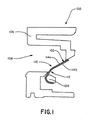
図1及び2は、一実施形態による、プラグが挿入される前の、及び挿入された後のジャックの概略断面図である。ジャック100は、主ハウジング106と、プラグインターフェース接触子102を支持するように配置されたスレッド104とを有する。スレッド104は、一以上の部材で構成されていてもよい。主ハウジング106及びスレッド104は、一以上の絶縁材で構成されており、プラグが挿入される空洞108を形成している。プラグインターフェース接触子102は、その一以上の点において、フレキシブルプリント回路を介して、硬質プリント回路基板(PCB)に電気的に接続されている。IDC(圧接接触子)が、PCBのスルーホールを介して背面からPCBに関わっている、他の実施形態においては、プラグインターフェース接触子は、PCB及びFPCの一方又は双方を使用することなく、IDCに接触する。IDCのための通路及びワイヤキャップを有するリアハウジングは、ツイストペア通信ケーブル又はパンチダウンブロックに対してインターフェースを提供する役目を果たしている。図1又は2には表れていないが、これらの特徴のいくつかは、図6−18の各種実施形態に示されている。
1 and 2 are schematic cross-sectional views of a jack before and after a plug is inserted, according to one embodiment. The
挿入前位置のプラグインターフェース接触子102が図1に示されている。挿入前位置において、プラグインターフェース接触子102はジャックハウジング106と接触するように示されているが、それらがジャックハウジング106と接触と接触しないような実施形態もある。図示された実施形態においては、各プラグインターフェース接触子102は、片持ち部110と屈曲部112の組み合わせからなる。屈曲部112は、スレッド104により保持されている。プラグインターフェース接触子102が曲がると、制約場所に、又はその近くに機械的応力集中が生じる。その応力が、プラグインターフェース接触子102を形成する材料の弾性限界を超えると、接触子の永久変形(へたり)が生じる。プラグインターフェース接触子102の形状は変形し、プラグのプラグ接触子と、ジャックのプラグインターフェース接触子との間の電気的接触に悪影響が生じ、それにより接触したりしなかったりになったり、または接触が途絶えてしまったりした。
The
永久変形を防止する方法としては、プラグインターフェース接触子102の厚さを薄くするということがある。しかしながら、プラグインターフェース接触子102の厚さを薄くすると、接触垂直抗力(すなわち、変位に対する抵抗)も減少する。所望の接触垂直抗力を維持し、同時に永久変形の可能性を減らすために、プラグインターフェース接触子102は、導電性条片の個々の(分かれた)層であるマルチ導電性層114a,114bを備えている。2枚のマルチ導電性層114a,114bのみが示されているが、何枚でも可能である。導電性層114a,114bは、空洞108内のプラグ/ジャックインターフェースのところ(すなわち、プラグ接触子が、ジャックのプラグインターフェース接触子と電気的及び機械的に接触するところ)で、又はその近くで、及び/又は最大機械的応力の場所で、互いに接触している。導電性層114a,114bは、同じサイズに示されているが、それらは、所望の特性に応じて異なる長さ、幅、又は厚さを有していてもよい。以下の具体的実施形態を参照しつつ、異なる寸法で導電性層114a,114bを形成する各種利点を説明する。
One method of preventing permanent deformation is to reduce the thickness of the
導電性層114a,114bは、同じ導電体で形成されていてもよいし、異なる導電体で形成されていてもよい。導電性層114a,114bを構成する各種導電体の例としては、銅、アルミニウム、金、銀、及びそれらの合金(例えば青銅)、ステンレススチール等の金属や、又は導電性粒子を含有した一般的絶縁材料がある。ある環境下においては、異なる材料を使用することが有利であろうが、各種方法による異なる材料の永久的重畳は問題も多く、構造特性を変化させてしまう可能性もある。また、異なる材料を使用すると、ガルバノ効果(異種金属接触腐食)が生ずる可能性もある。従って、いくつかの実施形態においては、同一材料の導電性層114a,114bでプラグインターフェース接触子112を作り上げるのが好ましい。
The
導電性層114a,114bは、特定の場所で所望の厚さを有するように互いに接触させて配設できる。その場所というのは、プラグインターフェース接触子102の最大応力及び/又はプラグ/ジャックインターフェースの位置である。導電性層114a,114bは、積層された原材料を圧搾して形成してもよいし、ジャック100を組みたてながら重ね合わせて形成してもよい。複数のプラグインターフェース接触子102の全部又は一部のみが、導電性層114a,114bから形成される。同様に、異なるプラグインターフェース接触子102が一組以上の異なる材料から形成される。
The
図2は、ジャック100の空洞108にプラグ260を挿入したところを示している。この図において、プラグ260は、空洞108内に十分深く挿入されて、プラグ接触子270がジャック100のプラグインターフェース接触子102に接触して挿入後の位置に押しやることとなる。導電性層114a,114bは、特定の場所で所望の厚さを有するように互いに接触させて配設できる。
FIG. 2 shows the
導電性層114a,114bは、その導電性層114a,114b全体に渡って固着されている必要はない。この場合、導電性層114a,114bは、プラグ260がプラグインターフェース接触子102の上側(又は外側)導電性層114aに接触するときに、互いにずれて動く。個々の導電性層114a,114bの薄さと相まって、このずれる動作により、各導電性層114a,114bは、永久変形することなく、プラグ160から受ける変位負荷に耐えることができる。いくつかの実施形態においては、導電性層114a,114bは、プラグの挿入に伴って下方に変位するので、図2に示すように、下側の(内側の)導電性層114bが、上側の導電性層114aよりも余計に延び、それにより変位差d1が生じる。一実施形態においては、導電性層114a,114bは、どの点でも互いに固着していない。また、他の実施形態においては、導電性層114a,114bは、両端のうちの一端、すなわち、スレッド104により保持されている一端又は空洞108内に配設されている一端、のところ、またはその近くで固着されている。導電性層114a,114bは、溶接、はんだ付け、締付け具、又は接着等の如何なる手段で固着されていてもよい。あるいは、又は加えて、導電性層114a,114bは、一以上の箇所で固着されていてもよく、そうでなければ、それらが互いに十分に摺動できて所望の接触垂直抗力が生じている限り、厚さ方向に制約されているようにしてもよい。例えば、プラグインターフェース接触子の一端が、スレッド104内に保持されているプリント回路基板(PCB)にはんだ付けされていてもよい。
The
導電性層の一層以上が、横(幅)方向に制約されていてもよく、それにより他の導電性層に接触する可能性が抑えられる。図3A及び3Bは、それぞれ、第一実施形態の断面図及び平面図であり、導電性層の一層316が実質的に導電性層310の全長さに渡って他の導電性層318を制約している。図3Aは、図3BのA−Aに沿って切って得られた断面図である。図3C及び3Dは、それぞれ、第二実施形態の斜視図及び断面図であり、導電性層の一層326(制約側)が、導電性層320の1以上の位置において他の導電性層328(被制約層)を制約している。第二実施形態においては、被制約層328は一方の側又は両側にノッチ(切欠き)324を有しており、制約側326は、各ノッチ324に嵌合するタブ322を有している。図3Dの断面図は、第二実施形態の一部分である、タブ322がノッチ324に重なる場所のものである。図3Dは、図3Cの平面Bに沿って得られた断面図である。
One or more of the conductive layers may be constrained in the lateral (width) direction, thereby reducing the possibility of contact with other conductive layers. 3A and 3B are a cross-sectional view and a plan view, respectively, of the first embodiment, where one
他の実施形態(図示せず)においては、制約側316は、1以上のタブを有しているが、非制約層328はノッチを1つも有していなくてもよい。あるいは、導電性層は、ノッチもタブも全く使用せずに横方向に制約されていてもよい。例えば、絶縁材料でできた1以上のバントが、少なくとも部分的に、プラグインターフェース接触子の一層以上の導電性層を取り囲むようにしてもよい。そのようなバンドは、導電性層が互いに長手方向に摺動するのを実質的に阻害する可能性もある。そのようなバンドを有した、又は有していない実施形態において、複数のプラグインターフェース接触子は、互いに機械的に隔絶されるように、絶縁体(例えばプラスチック)により分離されている。
In other embodiments (not shown), the constraining
ジャックの他の実施形態が、図4の概略断面図に示されている。同図において、図1と同様、プラグが挿入される前のジャック400が示されている。ジャック400は、主ハウジング406と、プラグインターフェース接触子410を支持するように配置されたスレッド404とから成っている。主ハウジング406とスレッド404とは、プラグが挿入される空洞408を形成している。プラグインターフェース接触子410は、誘電体層418により分離された導電性層414,416を備えている。上記のように、二層の導電性層と一層の誘電体層のみが示されているが、何層であってもよい。導電性層414,416は同じ材料で形成されていてもよいし、異なる材料で形成されていてもよく、同じサイズであってもよいし、異なるサイズであってもよい。誘電体層418は、同一材料又は異なる材料の一層以上で形成される。
Another embodiment of a jack is shown in the schematic cross-sectional view of FIG. In the same figure, the
導電性層414,416及び誘電体層418は、同調容量を形成してもよい。その容量においては、外側導電性層416がプラグのプラグ接触子に接触し、FPC又はPCB(図示せず)の第一ピン接触子に接続される。内側導電性層414は、回路基板の第二ピン接触子に接続される。容量を形成する導電性層は、空洞408の下方領域で、適切なピンに遷移できるようになっている。例えば、第三プラグインターフェース接触子の外側導電性層は、回路基板の第三ピン接触子に接続されており、一方、第三プラグインターフェース接触子の内側導電性層(及び第五プラグインターフェース接触子の外側導電性層)は、第五ピン接触子に接続されており、それにより3−5接触容量が形成されている。かかる容量は、プラグの45−36対の同調のために使用される。他の(例えば外側)導電性層についての容量を形成する一方の(例えば内側)導電性層の幅を短くすることにより、接触層間の大電位差による問題を排除し易くなっている。内側導電性層と特定のピンとの接続は、プラグの動きを妨げたり、他のピントの短絡が起きたりしないように設計される。
前記実施形態と同様、導電性層414,416及び誘電体層418は、互いに対して自由に動くことが可能であるか、1以上の方向に制約されている。加えて、上に示したように、導電性層414,416及び誘電体層418は、それらの各種層の全長さに渡って同じように伸びているが、それらの一層以上の各寸法の1以上の寸法が制限されていてもよい。例えば、それらの導電性層の一層が、他の導電性層より薄く又は狭くてもよく、また、誘電体層が導電性層と同一の厚さを有していてもよく、また異なる厚さを有していてもよい。導電性層の一層又は誘電体層の幅が狭くなると、導電性層間の平行板容量が同様に減少する。導電性層及び/又は誘電体層は、プラグインターフェース接触子の1以上の局所領域に設けられ、それによりプラグインターフェース接触子の電気的及び機械的特性を変更することができる。
As with the previous embodiment, the
プラグインターフェース接触子の機械的頑健性に加えて、コネクターのクロストーク(ノイズ)の削減のような、好適な電気的特性を提供することが望ましい。コネクターにおけるノイズ抑制の幅広い議論は、2005年7月13日出願の米国特許出願第11/180,216号、名称「フレキシブルプリント回路基板を有した通信コネクター」になされており、その内容は全てここに引用されているものとする。ノイズ補償回路の効果は、プラグ/ジャックインターフェースからの距離が短くなれば、増大する。 In addition to the mechanical robustness of the plug interface contacts, it is desirable to provide suitable electrical characteristics such as reduced connector crosstalk (noise). A broad discussion of noise suppression in connectors is given in US patent application Ser. No. 11 / 180,216, filed Jul. 13, 2005, entitled “Communication Connector with Flexible Printed Circuit Board”, all of which are here. Shall be quoted in The effect of the noise compensation circuit increases as the distance from the plug / jack interface decreases.
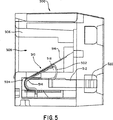
ジャックの他の実施形態の断面図が図5に示されており、スレッドの斜視図及び断面図が図6A−6Cに示されている。同図において、プラグが挿入される前のジャック500が示されている。ジャック500は、主ハウジング506と、プラグインターフェース接触子510を支持するように配置されたスレッド504とから成っている。主ハウジング506とスレッド504とは、プラグが挿入される空洞508を形成している。プラグインターフェース接触子510は、導電性層514,516と、導電性層514,516の間に配設されたフレキシブルプリント回路(FPC)502とを有している。具体的には、FPC502の一端は、空洞508内の本質的にプラグ/ジャックインターフェース部518の部分のみで導電性層514,516で挟まれている。FPC502の他端は、例えばはんだ付けにより、スレッド504に保持されたPCB512に接続されている。かかる構成を採用すると、接触子/FPCインターフェースがプラグ/ジャックインターフェース部518の部分にあることから、プラグインターフェース接触子510に流れる電流量を減らすことができる。そしてこれにより、クロストークや他のノイズ源が削減される。FPC502はフレキシブルであるので、プラグが挿入されると正確に一括して動いてしまうようなプラグインターフェース接触子の全てに接続することができる。FPC502は、隣接するプラグインターフェース接触子510の間に配設されていてもよく、または櫛形状に形成されて、PCB512に接触する箇所が実質的に矩形である一方、個々の素子がその矩形部から延びて個々のプラグインターフェース接触子510に接触するようになっていてもよい。
A cross-sectional view of another embodiment of the jack is shown in FIG. 5, and a perspective view and a cross-sectional view of the sled are shown in FIGS. 6A-6C. In the figure, the
他の実施形態では、導電性層514,516は同じ厚さを有しているが、示されている通り、上部導電性層516は、底部導電性層514よりも厚さが薄くなっている。底部導電性層514は、FPC502の保持するように構成されたオフセットを有している。そのような構成により、プラグ/ジャックインターフェース518からPCB512までの距離を最短にすることができる。PCB512の孔520は、圧接接触子(IDC)を備えることができる。導電性層514,516の一方又は双方のFPC502に近い端部は、丸くなっており、及び/又は削られて鋭利な角やバリが取り去られ、それによりFPC502を傷つける可能性を減らしている。導電性層514,516は、上で示した通り、自由であるか、又は制約されている。導電性層514,516が制約されている場合には、記述のように1以上の箇所で制約されているか、又はプラグインターフェース接触子502の本質的に長さ方向の全体に渡って制約されている。FPC502は、いろいろな箇所に、例えば、接触パッド、電流搬送線、並びに容量及び/又はインダクタンス領域等を有している。
In other embodiments, the
プラグインターフェース接触子及びFPCを介したプラグとPCBの間の電気的通信が有効になっている限り、PCBは、ジャック内の他の場所に配設されることも可能である。 The PCB can be placed elsewhere in the jack as long as electrical communication between the plug and PCB via the plug interface contacts and FPC is enabled.
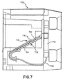
図7−13は、本発明による複数層接触子及びPCB配置の異なる実施形態を示している。図7−13において、同じ構成要素には同じ参照番号が付されている。図7のジャック700の一実施形態の断面図には、PCB712が水平(すなわち、プラグの動きの方向に平行)ではなく、垂直(すなわち、プラグの動きの方向に垂直)に配設されている。同図において、プラグが挿入される前のジャック700が示されている。プラグインターフェース接触子710は、導電性層714,716と、導電性層714,716の間に配設されたフレキシブルプリント回路(FPC)702と、を有している。FPC702は、導電性層714,716で挟まれている。FPC702の一端は、垂直に配設されたPCB712に接続されている。
Figures 7-13 show different embodiments of multi-layer contacts and PCB arrangement according to the present invention. 7-13, the same reference numerals are given to the same components. In the cross-sectional view of one embodiment of
プラグ(図示せず)が空洞に挿入されるとき、プラグのプラグ接触子(図示せず)は、FPC702上の接触子パッドを介してプラグ/ジャックインターフェース部718でFPC702と通信する。この実施形態で示される通り、底部導電性層714は、上部導電性層716よりも長く、それによりプラグ/ジャックインターフェース部718の近くのFPC702端部に相互接続容量を与えることができる。底部導電性層714は、プラグ/ジャックインターフェース部718に突起領域722も有している。突起領域722は、曲ってFPC702に接触する弧を形成しており、その突起領域722により、FPC702の接触パッド/線に対する底部接触子714の垂直抗力が増すようになっている。他の実施形態においては、上部導電性層716は、底部導電性層714よりも長くてもよい。
When a plug (not shown) is inserted into the cavity, the plug contact (not shown) of the plug communicates with the
図8は、本発明の他の実施形態による通信ジャック800の断面図である。プラグインターフェース接触子810は、異なる長さと厚さを有する導電性層814,816を有している。図8に示す実施形態においては、底部導電性層814は、上部導電性層816よりも厚く、プラグインターフェース接触子810の機械的力の主体となっている。底部導電性層814は、プラグ/ジャックインターフェース部818の近くで終端する。上部導電性層816は、底部導電性層814より更にプラグ/ジャックインターフェース部818から空洞内に延びる。上部導電性層816は、プラグ/ジャックインターフェース部818からジャック800の背部方向に延び、そこで、上部導電性層816は、鋭角を形成するように曲がる。上部導電性層816は、水平に配設されたPCB812の接触パッド824に接触する。
FIG. 8 is a cross-sectional view of a
図9は、ジャック900の他の実施形態の断面図である。プラグインターフェース接触子910は、異なる長さと厚さを有する導電性層914,916を有している。導電性層914,916は、FPC902により隔てられている。底部導電性層914は、上部導電性層916よりも厚く、プラグインターフェース接触子910の機械的力の主体となっている。底部導電性層914は、プラグ/ジャックインターフェース部918の近くで終端する。
FIG. 9 is a cross-sectional view of another embodiment of a
FPC902は、導電性層914,916の長さ全体に渡ってそれらの間に配設されている。FPC902は、図7に示された実施形態と同様、その一端が、垂直に配設されたPCB912に接続されている。底部導電性層914は、上部導電性層916よりも短い。上部導電性層916は、FPC902上の接触子パッドを介してプラグ/ジャックインターフェース部918でFPC902と通信する。底部導電性層914は、プラグ/ジャックインターフェース部918から離れた部分で、FPC902から僅かに離れるように形成されており、またプラグ/ジャックインターフェース部918においては、FPC902の接触パッド/線と接触する平坦突起部922を有している。その突起領域922により、プラグ/ジャックインターフェース部918における底部接触子914の垂直抗力が増すようになっている。FPC902は、底部導電性層914の突起領域902よりも更に延び、それによりプラグ/ジャックインターフェース部918の近くのFPC902端部に相互接続容量を与えることができる。
The
図10は、ジャック1000の他の実施形態の断面図である。プラグインターフェース接触子1010は、異なる長さと厚さを有する導電性層1014,1016を有している。導電性層1014,1016は、プラグ/ジャックインターフェース部1018とスレッド1004に保持された端部の間の少なくともいくつかの場所で接触している。底部導電性層1014は、上部導電性層1016よりも厚く、プラグインターフェース接触子1010の機械的力の主体となっている。底部導電性層1014は、プラグ/ジャックインターフェース部1018の近くで終端している一方、上部導電性層1016は、ジャック1000の空洞1008内を更に延びている。
FIG. 10 is a cross-sectional view of another embodiment of the
FPC1002は、本質的にプラグ/ジャックインターフェース部1018のところでのみ、導電性層1014,1016の間に配設されている。FPC1002は、その一端が、垂直に配設されたPCB1012に接続されている。上部導電性層1016は、FPC1002上の接触子パッドを介してプラグ/ジャックインターフェース部1018でFPC1002と通信する。底部導電性層1014は、プラグ/ジャックインターフェース部1018に配設されたFPC1002により、上部導電性層1016から僅かに離れている。あるいは、底部導電性層は、上記と同様、突起領域を有していてもよい。FPC1002は、電流搬送線及び容量領域を有している。
図11は、ジャック1100の他の実施形態の断面図である。プラグインターフェース接触子1110は、異なる長さと厚さを有する導電性層1114,1116を有している。底部導電性層1114は、上部導電性層1116よりも厚く、プラグインターフェース接触子1110の機械的力の主体となっている。底部導電性層1114は、プラグ/ジャックインターフェース部1118の近くで終端している。上部導電性層1116は、底部導電性層1114よりも更に延びている。
FIG. 11 is a cross-sectional view of another embodiment of a
FPC1102は、プラグ/ジャックインターフェース部1118のところで、導電性層1114,1116の間に配設されている。底部導電性層1114は、プラグ/ジャックインターフェース部1118から離れた部分で、FPC1102から僅かに離れており、またプラグ/ジャックインターフェース部1118においては、FPC1102と接触する平坦オフセット1122を有している。
The
FPC1102は二つ折にされており、その両端が、垂直に配設された1つ以上のPCB1112に接続されている。FPC1102は、各端部がはんだ付けによりPCB1112に接続されるようにしてもよい。FPC1102を二つ折にすることにより、組み立ての融通性を最大にしつつ、四層の線を使用することが可能となる。オフセット1122により十分に分離されているので、二つ折FPC1102は、上部導電性層1116と底部導電性層1114の間に適合できる。
The
図12は、一実施形態によるジャックの接触子アセンブリ1200の断面図である。接触子アセンブリ1200は、プラグインターフェース接触子1210が延びる本体1204を有している。プラグインターフェース接触子1210は、異なる長さと厚さを有する導電性層1214,1216を有している。プラグインターフェース接触子1210は、本体1204により保持されている。導電性層1214,1216は、プラグ/ジャックインターフェース部1218から本体1204内で保持される一端まで延設されている。プラグインターフェース接触子1210は、本体1204から延びるピン1230に接続される。導電性層1214,1216は、プラグ/ジャックインターフェース部1218と本体1204内に保持された端部の間の少なくともいくつかの場所で接触している。底部導電性層1214は、上部導電性層1216よりも厚く、プラグインターフェース接触子1210の機械的力の主体となっている。底部導電性層1214は、プラグ/ジャックインターフェース部1218の近くで終端している一方、上部導電性層1216は、底部導電性層1214よりも更に延びている。フレキシブルキャパシター1226が、プラグ/ジャックインターフェース部1218のところで導電性層1214,1216の間に配設されている。これにより、プラグ/ジャックインターフェース部1218とキャパシター1226の容量との間の距離を短くすることができる。
FIG. 12 is a cross-sectional view of a
図13は、図11に示した実施形態と同様のジャック1300の他の実施形態の断面図である。プラグインターフェース接触子1310は、異なる長さと厚さを有する導電性層1314,1316を有している。導電性層1314,1316は、プラグ/ジャックインターフェース部1318とスレッドに保持された端部の間の少なくともいくつかの場所で接触している。底部導電性層1314は、等しい厚さの副層1314a,1314bで構成されている。副層1314a,1314bの各々の厚さは、上部導電性層1316の厚さに等しい。つまり、底部導電性層1314は、上部導電性層1316の約2倍であり、プラグインターフェース接触子1310の機械的力の主体となっている。他の実施形態においては、上部導電性層1316と副層1314a,1314bの各々の相対的厚さは、要望に応じて変更可能である。例えば、副層1314a,1314bは、同じ厚さを有していてもよいし、異なる厚さを有していてもよく、また、副層1314a,1314bの一方又は双方が上部導電性層1316と異なる厚さを有していてもよい。底部導電性層1314は、プラグ/ジャックインターフェース部1318の近くで終端している一方、上部導電性層1316は、ジャック1300の空洞1308内に更に延びている。
FIG. 13 is a cross-sectional view of another embodiment of a
FPC1302は、プラグ/ジャックインターフェース部1318のところでのみ、導電性層1314,1316の間に配設されている。FPC1302は、その一端が、垂直に配設されたPCB1312に接続されている。底部導電性層1314は、上部導電性層1316よりも短い。プラグ(図示せず)が空洞1308に挿入されると、プラグのプラグ接触子(図示せず)は、FPC1302上の接触子パッドを介してプラグ/ジャックインターフェース部1318でFPC1302と通信する。底部導電性層1314は、プラグ/ジャックインターフェース部1318に配設されたFPC1302により、上部導電性層1316から僅かに離れている。
The
上に示したように、上記実施形態のいずれの特徴も可能な方法で組み合わせることも可能である。ジャックの各種実施形態は、通信機器等のあらゆる装置に使用可能である。例えば、ジャックを、壁付きコンセント、コンピュータ等のエンドユーザー機器、パッチパネル等の中間域機器、又はネットワークマネージャー等のネットワーク機器に組み込むことは有益である。 As indicated above, any of the features of the above embodiments can be combined in a possible manner. Various embodiments of the jack can be used in any device such as a communication device. For example, it may be beneficial to incorporate the jack into a wall outlet, an end user device such as a computer, a mid-range device such as a patch panel, or a network device such as a network manager.
各種の上で開示された特徴及び機能や他の特徴及び機能、又は択一的特徴及び機能が、要望に応じて組み合わされて他の異なるシステムや応用品となり得る。例えば、単数は、1つ以上の構成要素の使用を意図している。ここで提示されているものは、限定ではなく例示である。また、現在予想されない多態形又は予見されない択一形、変形、その多態形又は改良形は、当業者によれば結果的に形成可能であり、以下の請求の範囲より包含されていると意図されている。 Various features and functions disclosed above, other features and functions, or alternative features and functions may be combined as desired to provide other different systems and applications. For example, the singular contemplates the use of one or more components. What is presented here is illustrative rather than limiting. In addition, polymorphs that are not currently anticipated or alternatives that are not foreseen, variations, polymorphs, or improvements thereof can be formed by those skilled in the art, and are encompassed by the following claims. Is intended.
Claims (17)
前記通信プラグを受け入れるように構成された空洞と、
前記空洞内に延びる複数のプラグインターフェース接触子と、
を備え、
前記空洞内のプラグが、前記プラグインターフェース接触子のプラグ/ジャックインターフェース部において前記プラグインターフェース接触子と電気的に接触し、前記プラグインターフェース接触子の少なくとも1つが、同じ材料で形成される個々の複数層導電性条片を備え、
前記導電性条片の少なくとも1つは、制約体により横方向に制約されて、被制約層を形成しており、
前記制約体は、前記被制約層の少なくとも一側面に隣接した、他の前記導電性条片の少なくとも1つであることを特徴とする通信ジャック。A communication jack configured to accept a communication plug to form a communication connector;
A cavity configured to receive the communication plug;
A plurality of plug interface contacts extending into the cavity;
With
A plug in the cavity is in electrical contact with the plug interface contact at a plug / jack interface portion of the plug interface contact, wherein at least one of the plug interface contacts is formed of the same material. for example Bei the layer conductive strip,
At least one of the conductive strips is constrained in the lateral direction by a constraining body to form a constrained layer,
The communication jack according to claim 1, wherein the restriction body is at least one of the other conductive strips adjacent to at least one side surface of the restricted layer .
前記通信プラグを受け入れるように構成された空洞と、
前記空洞内に延びる複数のプラグインターフェース接触子と、
を備え、
前記空洞内のプラグが、前記プラグインターフェース接触子のプラグ/ジャックインターフェース部において前記プラグインターフェース接触子と電気的に接触し、前記プラグインターフェース接触子の少なくとも1つが、その金属層の少なくとも一端において互いに長手方向に移動可能な複数の導電性層を備え、
前記導電性層の少なくとも一層は、制約体により横方向に制約されて、被制約層を形成しており、
前記制約体は、前記被制約層の少なくとも一側面に隣接した、他の前記導電性条片の少なくとも1つであることを特徴とする通信ジャック。A communication jack configured to accept a communication plug to form a communication connector;
A cavity configured to receive the communication plug;
A plurality of plug interface contacts extending into the cavity;
With
Plugs in the cavity are in electrical contact with the plug interface contacts at the plug / jack interface portion of the plug interface contact, and at least one of the plug interface contacts extends longitudinally from at least one end of the metal layer. e Bei a plurality of conductive layer movable in a direction,
At least one of the conductive layers is constrained in a lateral direction by a constraint body to form a constrained layer,
The communication jack according to claim 1, wherein the restriction body is at least one of the other conductive strips adjacent to at least one side surface of the restricted layer .
前記通信プラグを受け入れるように構成された空洞と、
前記空洞内に延びる複数のプラグインターフェース接触子と、
を備え、
前記空洞内のプラグが、前記プラグインターフェース接触子のプラグ/ジャックインターフェース部において前記プラグインターフェース接触子と電気的に接触し、前記プラグインターフェース接触子の少なくとも1つが、その厚さ方向には制約されているが、その少なくとも一端において互いに長手方向に移動可能な複数の導電性層を備え、
前記導電性層は、その一端の近傍に配設された制約体により制約されていることを特徴とする通信ジャック。A communication jack configured to accept a communication plug to form a communication connector;
A cavity configured to receive the communication plug;
A plurality of plug interface contacts extending into the cavity;
With
A plug in the cavity is in electrical contact with the plug interface contact at a plug / jack interface portion of the plug interface contact, and at least one of the plug interface contacts is restricted in its thickness direction. It is but Bei to give a plurality of conductive layers longitudinally movable to each other in at least one end,
The communication jack is characterized in that the conductive layer is restricted by a restriction body disposed in the vicinity of one end thereof .
Applications Claiming Priority (3)
| Application Number | Priority Date | Filing Date | Title |
|---|---|---|---|
| US86983406P | 2006-12-13 | 2006-12-13 | |
| US60/869,834 | 2006-12-13 | ||
| PCT/US2007/087410 WO2008076813A2 (en) | 2006-12-13 | 2007-12-13 | Communication jack having layered plug interface contacts |
Publications (3)
| Publication Number | Publication Date |
|---|---|
| JP2010514104A JP2010514104A (en) | 2010-04-30 |
| JP2010514104A5 JP2010514104A5 (en) | 2011-01-13 |
| JP4944210B2 true JP4944210B2 (en) | 2012-05-30 |
Family
ID=39482408
Family Applications (1)
| Application Number | Title | Priority Date | Filing Date |
|---|---|---|---|
| JP2009541588A Expired - Fee Related JP4944210B2 (en) | 2006-12-13 | 2007-12-13 | Communication jack with multi-layer plug interface contacts |
Country Status (6)
| Country | Link |
|---|---|
| US (6) | US7874877B2 (en) |
| EP (1) | EP2102947B1 (en) |
| JP (1) | JP4944210B2 (en) |
| CN (1) | CN101584089B (en) |
| AT (1) | ATE531103T1 (en) |
| WO (1) | WO2008076813A2 (en) |
Cited By (1)
| Publication number | Priority date | Publication date | Assignee | Title |
|---|---|---|---|---|
| JP2019511825A (en) * | 2016-04-13 | 2019-04-25 | パンドウィット・コーポレーション | Communication jack with dielectric film between plug interface contacts |
Families Citing this family (24)
| Publication number | Priority date | Publication date | Assignee | Title |
|---|---|---|---|---|
| CN102082367B (en) | 2004-03-12 | 2013-11-20 | 泛达公司 | Methods and apparatus for reducing crosstalk in electrical connectors |
| CN101584089B (en) * | 2006-12-13 | 2012-06-13 | 泛达公司 | Communication jack having layered plug interface contacts |
| WO2011005972A1 (en) * | 2009-07-10 | 2011-01-13 | Panduit Corp. | Communications connector with a short conductive path to compensation |
| US8641452B2 (en) | 2011-03-22 | 2014-02-04 | Panduit Corp. | Communication jack having an insulating element connecting a spring element and a spring end of a contact element |
| US8568176B2 (en) * | 2011-06-03 | 2013-10-29 | Telebox Industries Corp. | Terminal module for electric connector |
| US9653847B2 (en) | 2013-01-11 | 2017-05-16 | Sentinel Connector System, Inc. | High speed communication jack |
| US8858266B2 (en) * | 2012-02-13 | 2014-10-14 | Sentinel Connector Systems, Inc. | High speed communication jack |
| US9337592B2 (en) | 2012-02-13 | 2016-05-10 | Sentinel Connector Systems, Inc. | High speed communication jack |
| US9627816B2 (en) | 2012-02-13 | 2017-04-18 | Sentinel Connector System Inc. | High speed grounded communication jack |
| US9239633B1 (en) | 2012-09-07 | 2016-01-19 | Google Inc. | System and method for device having internal reset/restart button that is activated via insertion tool accessiable throught single transmission path of plug connection |
| EP2763243B1 (en) * | 2013-01-30 | 2017-06-07 | Alcatel-Lucent Shanghai Bell Co., Ltd. | Connecting element and method of manufacturing a connecting element |
| US9118134B2 (en) * | 2013-03-01 | 2015-08-25 | Panduit Corp. | RJ-45-compatible communication connector with contacts having wider distal ends |
| EP3134945B1 (en) * | 2014-04-23 | 2019-06-12 | TE Connectivity Corporation | Electrical connector with shield cap and shielded terminals |
| US9865960B2 (en) * | 2014-09-04 | 2018-01-09 | Belden Canada Inc. | Coupler connector and cable terminator with side contacts |
| RU2017114931A (en) | 2014-10-01 | 2018-11-02 | Сентинл Коннектор Системз, Инк. | HIGH SPEED CONNECTOR |
| US9966703B2 (en) | 2014-10-17 | 2018-05-08 | Panduit Corp. | Communication connector |
| US10050383B2 (en) * | 2015-05-19 | 2018-08-14 | Panduit Corp. | Communication connectors |
| US9912083B2 (en) | 2015-07-21 | 2018-03-06 | Sentinel Connector Systems, Inc. | High speed plug |
| EP3375052A1 (en) * | 2015-11-11 | 2018-09-19 | Bel Fuse (Macao Commercial Offshore) Limited | Modular jack connector |
| US20170317450A1 (en) * | 2016-04-29 | 2017-11-02 | Panduit Corp. | RJ Communication Connectors |
| US9899765B2 (en) | 2016-05-04 | 2018-02-20 | Sentinel Connector Systems, Inc. | Large conductor industrial plug |
| US9985373B2 (en) * | 2016-10-12 | 2018-05-29 | Surtec Industries, Inc. | Communication connector |
| US10361514B2 (en) * | 2017-03-02 | 2019-07-23 | Panduit Corp. | Communication connectors utilizing multiple contact points |
| US10530106B2 (en) | 2018-01-31 | 2020-01-07 | Bel Fuse (Macao Commercial Offshore) Limited | Modular plug connector with multilayer PCB for very high speed applications |
Family Cites Families (48)
| Publication number | Priority date | Publication date | Assignee | Title |
|---|---|---|---|---|
| US2755453A (en) * | 1952-08-06 | 1956-07-17 | Metals & Controls Corp | Electrical terminal |
| DE1802130A1 (en) * | 1968-10-09 | 1970-04-23 | Siemens Ag | Multiple plug |
| US4367907A (en) * | 1980-08-04 | 1983-01-11 | Magnetic Controls Company | Circuit monitoring jack |
| KR890004702Y1 (en) | 1983-03-15 | 1989-07-15 | 호시덴기세이조오 가부시기가이샤 | Telephone connector |
| US4720269A (en) | 1987-03-10 | 1988-01-19 | Northern Telecom Limited | Modular telephone jack with elastomeric contact member |
| US5004426A (en) * | 1989-09-19 | 1991-04-02 | Teradyne, Inc. | Electrically connecting |
| US5230632A (en) | 1991-12-19 | 1993-07-27 | International Business Machines Corporation | Dual element electrical contact and connector assembly utilizing same |
| US5240420A (en) * | 1992-03-31 | 1993-08-31 | Research Organization For Circuit Knowledge | Self-aligning high-density printed circuit connector |
| JP3380913B2 (en) | 1992-06-11 | 2003-02-24 | ソニー株式会社 | Solid-state imaging device |
| US5328390A (en) * | 1992-09-01 | 1994-07-12 | Hubbell Incorporated | Modular telecommunication jack adapter |
| US5810620A (en) * | 1992-10-29 | 1998-09-22 | Olympus Optical Co., Ltd. | Electric connector provided with a shielding part for electrical contacts at the distal end of the plug |
| US5639266A (en) * | 1994-01-11 | 1997-06-17 | Stewart Connector Systems, Inc. | High frequency electrical connector |
| US5716237A (en) * | 1996-06-21 | 1998-02-10 | Lucent Technologies Inc. | Electrical connector with crosstalk compensation |
| CA2182438C (en) * | 1996-07-31 | 2001-05-29 | Peter Craig | Circuit connector |
| US5971806A (en) * | 1997-11-26 | 1999-10-26 | Berg Technology, Inc. | Electrical connector for connecting conductor areas of a flexible circuit with associated conductor pads of a circuit board |
| US5957734A (en) * | 1998-01-21 | 1999-09-28 | General Motors Corporation | Tuning fork inline connection system |
| JP2000077125A (en) * | 1998-08-28 | 2000-03-14 | Kel Corp | Male-and-female fitting type connector |
| US6238225B1 (en) * | 1998-09-23 | 2001-05-29 | Tvm Group, Inc. | Bus bar assembly |
| CA2291373C (en) * | 1998-12-02 | 2002-08-06 | Nordx/Cdt, Inc. | Modular connectors with compensation structures |
| US6375516B1 (en) | 1999-02-24 | 2002-04-23 | Xircom, Inc. | RJ-45 receptacle with stops preventing insertion of RJ-11 plugs |
| US6220900B1 (en) | 1999-10-27 | 2001-04-24 | Hon Hai Precision Ind. Co., Ltd. | Low profile electrical connector assembly with low insertion force |
| US6360437B1 (en) | 2000-03-15 | 2002-03-26 | Japan Aviation Electronics Industry, Limited | Electrical contact having surface coating layer with irregular surface due to hard particles dispersed in the surface coating layer |
| US6283796B1 (en) | 2000-03-23 | 2001-09-04 | Hon Hai Precision Ind. Co., Ltd. | RJ-receptacle connector with anti-incorrect-insertion device |
| US6402560B1 (en) * | 2000-05-31 | 2002-06-11 | Avaya Technology Corp. | Communication connector with crosstalk compensation |
| TW456610U (en) | 2000-07-12 | 2001-09-21 | Hon Hai Prec Ind Co Ltd | Socket connector |
| US6244907B1 (en) | 2000-08-02 | 2001-06-12 | Avaya Technology Corp. | Selectable compatibility electrical connector assembly |
| TW454993U (en) | 2000-08-08 | 2001-09-11 | Hon Hai Prec Ind Co Ltd | Socket connector |
| US6780035B2 (en) * | 2001-03-12 | 2004-08-24 | Nordx/Cdt, Inc. | Electrostatic discharge protected jack |
| FR2828590B1 (en) * | 2001-08-08 | 2003-09-26 | Framatome Connectors Int | BUS BAR |
| JP2003142183A (en) * | 2001-11-01 | 2003-05-16 | Fujitsu Component Ltd | Contact module, connector and manufacturing method for contact module |
| US6767257B2 (en) | 2002-01-04 | 2004-07-27 | Avaya Technology Corp. | Communication jack that withstands insertion of a communication plug that the jack is not specifically configured to mate with without being damage |
| US6736681B2 (en) | 2002-10-03 | 2004-05-18 | Avaya Technology Corp. | Communications connector that operates in multiple modes for handling multiple signal types |
| US7059907B2 (en) * | 2003-07-24 | 2006-06-13 | Fci Americas Technology, Inc. | Modular electrical connector |
| DE10352761B4 (en) * | 2003-11-12 | 2006-06-08 | Wolf Neumann-Henneberg | Connection contact for electrical contacting of a printed circuit board or a punched grid |
| US7125288B2 (en) | 2003-12-16 | 2006-10-24 | Bel-Fuse Inc. | Preventing damage to RJ jacks from improper plug insertion |
| US7179131B2 (en) * | 2004-02-12 | 2007-02-20 | Panduit Corp. | Methods and apparatus for reducing crosstalk in electrical connectors |
| CN102082367B (en) * | 2004-03-12 | 2013-11-20 | 泛达公司 | Methods and apparatus for reducing crosstalk in electrical connectors |
| US7153168B2 (en) * | 2004-04-06 | 2006-12-26 | Panduit Corp. | Electrical connector with improved crosstalk compensation |
| EP1774625B1 (en) * | 2004-07-13 | 2014-06-25 | Panduit Corporation | Communications connector with flexible printed circuit board |
| EP1643599B1 (en) * | 2004-09-29 | 2008-12-17 | Sumitomo Wiring Systems, Ltd. | A terminal fitting and a connector using such a terminal fitting |
| US7104812B1 (en) | 2005-02-24 | 2006-09-12 | Molex Incorporated | Laminated electrical terminal |
| US7357683B2 (en) * | 2005-07-15 | 2008-04-15 | Panduit Corp. | Communications connector with crimped contacts |
| CN101584089B (en) * | 2006-12-13 | 2012-06-13 | 泛达公司 | Communication jack having layered plug interface contacts |
| DE102007005959A1 (en) * | 2007-02-06 | 2008-08-14 | Adc Gmbh | Connectors |
| US7967645B2 (en) * | 2007-09-19 | 2011-06-28 | Leviton Manufacturing Co., Inc. | High speed data communications connector circuits, systems, and methods for reducing crosstalk in communications systems |
| US7601034B1 (en) * | 2008-05-07 | 2009-10-13 | Ortronics, Inc. | Modular insert and jack including moveable reactance section |
| WO2011005972A1 (en) * | 2009-07-10 | 2011-01-13 | Panduit Corp. | Communications connector with a short conductive path to compensation |
| EP2403069B1 (en) * | 2010-07-02 | 2017-05-17 | Nexans | Communication assembly comprising a plug connector and a jack assembly provided to be connected |
-
2007
- 2007-12-13 CN CN2007800462193A patent/CN101584089B/en not_active Expired - Fee Related
- 2007-12-13 JP JP2009541588A patent/JP4944210B2/en not_active Expired - Fee Related
- 2007-12-13 WO PCT/US2007/087410 patent/WO2008076813A2/en active Application Filing
- 2007-12-13 US US11/955,699 patent/US7874877B2/en active Active
- 2007-12-13 AT AT07869226T patent/ATE531103T1/en not_active IP Right Cessation
- 2007-12-13 EP EP07869226A patent/EP2102947B1/en not_active Not-in-force
-
2011
- 2011-01-14 US US13/007,118 patent/US8105116B2/en not_active Expired - Fee Related
-
2012
- 2012-01-30 US US13/360,899 patent/US8435084B2/en active Active
-
2013
- 2013-05-03 US US13/886,702 patent/US8758060B2/en not_active Expired - Fee Related
-
2014
- 2014-05-05 US US14/269,356 patent/US8992264B2/en not_active Expired - Fee Related
-
2015
- 2015-03-27 US US14/670,942 patent/US9281632B2/en not_active Expired - Fee Related
Cited By (2)
| Publication number | Priority date | Publication date | Assignee | Title |
|---|---|---|---|---|
| JP2019511825A (en) * | 2016-04-13 | 2019-04-25 | パンドウィット・コーポレーション | Communication jack with dielectric film between plug interface contacts |
| JP7282522B2 (en) | 2016-04-13 | 2023-05-29 | パンドウィット・コーポレーション | Communication jack with dielectric film between plug interface contacts |
Also Published As
| Publication number | Publication date |
|---|---|
| US8105116B2 (en) | 2012-01-31 |
| US8758060B2 (en) | 2014-06-24 |
| EP2102947B1 (en) | 2011-10-26 |
| WO2008076813A3 (en) | 2008-08-21 |
| WO2008076813A2 (en) | 2008-06-26 |
| US20140256191A1 (en) | 2014-09-11 |
| US9281632B2 (en) | 2016-03-08 |
| US20120129404A1 (en) | 2012-05-24 |
| US20080146093A1 (en) | 2008-06-19 |
| US20130288538A1 (en) | 2013-10-31 |
| CN101584089B (en) | 2012-06-13 |
| CN101584089A (en) | 2009-11-18 |
| JP2010514104A (en) | 2010-04-30 |
| US8435084B2 (en) | 2013-05-07 |
| US7874877B2 (en) | 2011-01-25 |
| US8992264B2 (en) | 2015-03-31 |
| ATE531103T1 (en) | 2011-11-15 |
| US20150200507A1 (en) | 2015-07-16 |
| EP2102947A2 (en) | 2009-09-23 |
| US20110111645A1 (en) | 2011-05-12 |
Similar Documents
| Publication | Publication Date | Title |
|---|---|---|
| JP4944210B2 (en) | Communication jack with multi-layer plug interface contacts | |
| JP7200286B2 (en) | Shape memory alloy wire mounting structure for suspension assembly | |
| JP5092243B2 (en) | Narrow pitch flexible wiring | |
| JP4881291B2 (en) | Method and apparatus for reducing crosstalk in electrical connectors | |
| CN103515730B (en) | Without cage adapter | |
| JP4906964B2 (en) | Coaxial harness connection structure | |
| US9318820B2 (en) | Connector for multi-layered board | |
| JPS6056380A (en) | Circuit board conductor unnecessary for soldering | |
| WO2021106546A1 (en) | Press-fit terminal, substrate with press-fit terminal, and device | |
| JP4910895B2 (en) | Card edge connector connection structure | |
| JP2006019025A (en) | Connector | |
| JP3977636B2 (en) | Flat flexible cable connector | |
| JP2008177148A (en) | Connector | |
| JP3126063U (en) | Pattern connection structure on circuit board | |
| JPH0543489U (en) | Connection structure of card type board and connector | |
| JP2010045724A (en) | Electronic apparatus | |
| JP2007173140A (en) | Flat circuit body |
Legal Events
| Date | Code | Title | Description |
|---|---|---|---|
| A521 | Request for written amendment filed |
Free format text: JAPANESE INTERMEDIATE CODE: A523 Effective date: 20101117 |
|
| A621 | Written request for application examination |
Free format text: JAPANESE INTERMEDIATE CODE: A621 Effective date: 20101117 |
|
| TRDD | Decision of grant or rejection written | ||
| A01 | Written decision to grant a patent or to grant a registration (utility model) |
Free format text: JAPANESE INTERMEDIATE CODE: A01 Effective date: 20120131 |
|
| A01 | Written decision to grant a patent or to grant a registration (utility model) |
Free format text: JAPANESE INTERMEDIATE CODE: A01 |
|
| A61 | First payment of annual fees (during grant procedure) |
Free format text: JAPANESE INTERMEDIATE CODE: A61 Effective date: 20120301 |
|
| R150 | Certificate of patent or registration of utility model |
Free format text: JAPANESE INTERMEDIATE CODE: R150 |
|
| FPAY | Renewal fee payment (event date is renewal date of database) |
Free format text: PAYMENT UNTIL: 20150309 Year of fee payment: 3 |
|
| LAPS | Cancellation because of no payment of annual fees |