CN106354674B - Semiconductor device and system - Google Patents
Semiconductor device and system Download PDFInfo
- Publication number
- CN106354674B CN106354674B CN201610478818.3A CN201610478818A CN106354674B CN 106354674 B CN106354674 B CN 106354674B CN 201610478818 A CN201610478818 A CN 201610478818A CN 106354674 B CN106354674 B CN 106354674B
- Authority
- CN
- China
- Prior art keywords
- data
- reception
- transmission
- data transfer
- mode
- Prior art date
- Legal status (The legal status is an assumption and is not a legal conclusion. Google has not performed a legal analysis and makes no representation as to the accuracy of the status listed.)
- Active
Links
Images


Classifications
-
- G—PHYSICS
- G06—COMPUTING; CALCULATING OR COUNTING
- G06F—ELECTRIC DIGITAL DATA PROCESSING
- G06F13/00—Interconnection of, or transfer of information or other signals between, memories, input/output devices or central processing units
- G06F13/38—Information transfer, e.g. on bus
- G06F13/42—Bus transfer protocol, e.g. handshake; Synchronisation
- G06F13/4282—Bus transfer protocol, e.g. handshake; Synchronisation on a serial bus, e.g. I2C bus, SPI bus
-
- G—PHYSICS
- G06—COMPUTING; CALCULATING OR COUNTING
- G06F—ELECTRIC DIGITAL DATA PROCESSING
- G06F13/00—Interconnection of, or transfer of information or other signals between, memories, input/output devices or central processing units
- G06F13/38—Information transfer, e.g. on bus
- G06F13/382—Information transfer, e.g. on bus using universal interface adapter
- G06F13/385—Information transfer, e.g. on bus using universal interface adapter for adaptation of a particular data processing system to different peripheral devices
-
- G—PHYSICS
- G06—COMPUTING; CALCULATING OR COUNTING
- G06F—ELECTRIC DIGITAL DATA PROCESSING
- G06F13/00—Interconnection of, or transfer of information or other signals between, memories, input/output devices or central processing units
- G06F13/38—Information transfer, e.g. on bus
- G06F13/40—Bus structure
- G06F13/4063—Device-to-bus coupling
- G06F13/4068—Electrical coupling
- G06F13/4072—Drivers or receivers
-
- G—PHYSICS
- G06—COMPUTING; CALCULATING OR COUNTING
- G06F—ELECTRIC DIGITAL DATA PROCESSING
- G06F13/00—Interconnection of, or transfer of information or other signals between, memories, input/output devices or central processing units
- G06F13/38—Information transfer, e.g. on bus
- G06F13/42—Bus transfer protocol, e.g. handshake; Synchronisation
- G06F13/4282—Bus transfer protocol, e.g. handshake; Synchronisation on a serial bus, e.g. I2C bus, SPI bus
- G06F13/4291—Bus transfer protocol, e.g. handshake; Synchronisation on a serial bus, e.g. I2C bus, SPI bus using a clocked protocol
-
- G—PHYSICS
- G06—COMPUTING; CALCULATING OR COUNTING
- G06F—ELECTRIC DIGITAL DATA PROCESSING
- G06F15/00—Digital computers in general; Data processing equipment in general
- G06F15/76—Architectures of general purpose stored program computers
- G06F15/80—Architectures of general purpose stored program computers comprising an array of processing units with common control, e.g. single instruction multiple data processors
- G06F15/8053—Vector processors
- G06F15/8076—Details on data register access
-
- H—ELECTRICITY
- H03—ELECTRONIC CIRCUITRY
- H03K—PULSE TECHNIQUE
- H03K19/00—Logic circuits, i.e. having at least two inputs acting on one output; Inverting circuits
- H03K19/0175—Coupling arrangements; Interface arrangements
- H03K19/017509—Interface arrangements
-
- H—ELECTRICITY
- H03—ELECTRONIC CIRCUITRY
- H03K—PULSE TECHNIQUE
- H03K23/00—Pulse counters comprising counting chains; Frequency dividers comprising counting chains
- H03K23/40—Gating or clocking signals applied to all stages, i.e. synchronous counters
- H03K23/50—Gating or clocking signals applied to all stages, i.e. synchronous counters using bi-stable regenerative trigger circuits
- H03K23/502—Gating or clocking signals applied to all stages, i.e. synchronous counters using bi-stable regenerative trigger circuits with a base or a radix other than a power of two
- H03K23/507—Gating or clocking signals applied to all stages, i.e. synchronous counters using bi-stable regenerative trigger circuits with a base or a radix other than a power of two with a base which is a non-integer
-
- H—ELECTRICITY
- H04—ELECTRIC COMMUNICATION TECHNIQUE
- H04B—TRANSMISSION
- H04B1/00—Details of transmission systems, not covered by a single one of groups H04B3/00 - H04B13/00; Details of transmission systems not characterised by the medium used for transmission
- H04B1/38—Transceivers, i.e. devices in which transmitter and receiver form a structural unit and in which at least one part is used for functions of transmitting and receiving
- H04B1/40—Circuits
- H04B1/401—Circuits for selecting or indicating operating mode
-
- H—ELECTRICITY
- H04—ELECTRIC COMMUNICATION TECHNIQUE
- H04B—TRANSMISSION
- H04B1/00—Details of transmission systems, not covered by a single one of groups H04B3/00 - H04B13/00; Details of transmission systems not characterised by the medium used for transmission
- H04B1/38—Transceivers, i.e. devices in which transmitter and receiver form a structural unit and in which at least one part is used for functions of transmitting and receiving
- H04B1/40—Circuits
- H04B1/44—Transmit/receive switching
-
- Y—GENERAL TAGGING OF NEW TECHNOLOGICAL DEVELOPMENTS; GENERAL TAGGING OF CROSS-SECTIONAL TECHNOLOGIES SPANNING OVER SEVERAL SECTIONS OF THE IPC; TECHNICAL SUBJECTS COVERED BY FORMER USPC CROSS-REFERENCE ART COLLECTIONS [XRACs] AND DIGESTS
- Y02—TECHNOLOGIES OR APPLICATIONS FOR MITIGATION OR ADAPTATION AGAINST CLIMATE CHANGE
- Y02D—CLIMATE CHANGE MITIGATION TECHNOLOGIES IN INFORMATION AND COMMUNICATION TECHNOLOGIES [ICT], I.E. INFORMATION AND COMMUNICATION TECHNOLOGIES AIMING AT THE REDUCTION OF THEIR OWN ENERGY USE
- Y02D10/00—Energy efficient computing, e.g. low power processors, power management or thermal management
Abstract
The invention relates to a semiconductor device and a system. The SCI may perform transmit only or receive only, however, the SCI must be reset when the transmission and reception are switched to transmit only or receive only. A semiconductor device includes an interface circuit that performs sequential communication of transmission or reception according to a synchronous clock. The interface circuit includes: a register for specifying an operation enable state as at least one of a transmission state and a reception state; and a mode control circuit for changing at least one of transmission or reception in the operation enable state.
Description
Cross Reference to Related Applications
The disclosure of Japanese patent application No.2015-141224 filed on 7/15/2015, which includes specification, drawings and abstract, is incorporated herein by reference in its entirety.
Technical Field
The present disclosure relates to a semiconductor device and is applicable to, for example, a semiconductor device provided with a Serial Communication Interface (SCI).
Background
Microcomputers including semiconductor integrated circuits are commonly used in appliance control applications. SCI is used for communication between microcomputers (for example, japanese unexamined patent application publication No. 2011-. SCI sends or receives data on a bit-by-bit basis. SCI in the clock synchronization mode performs transmission and reception, thereby defining a period from a specific falling edge of a clock to the next falling edge as 1 bit. The simultaneous transmit-receive operation is performed by three lines, a clock line, a transmit line and a receive line. Clock synchronization systems are used for relatively high-speed communications.
(patent document 1) Japanese unexamined patent application publication No.2011-
Disclosure of Invention
The SCI may perform transmit-only or receive-only. However, the SCI must be reset when transmission and reception are switched to transmit only or receive only.
Other problems and novel features of the invention will become apparent from the description of the invention and the drawings.
An overview of exemplary embodiments of the present disclosure is briefly described below. That is, the semiconductor device includes an interface circuit that performs sequential communication of transmission or reception. The interface circuit includes: a register for specifying an operation enable state as at least one of a transmission state and a reception state; and a mode control circuit for changing at least one of transmission or reception in the operation enable state.
According to the semiconductor device described above, the transmission mode or the reception mode can be easily changed.
Drawings
Fig. 1A is a block diagram for explaining a configuration of a microcomputer according to an implementation example;
fig. 1B is a block diagram illustrating a host interface of the microcomputer illustrated in fig. 1A;
FIG. 2 is a block diagram illustrating the construction of the SCI shown in FIG. 1A;
FIG. 3 is a diagram showing the register structure of the SCI shown in FIG. 1A;
FIG. 4 is a diagram illustrating mode control state transitions of the SCI illustrated in FIG. 1A;
FIG. 5 is a block diagram showing the configuration of the interrupt controller shown in FIG. 1A;
fig. 6 is a diagram illustrating data transmission information of the DTC illustrated in fig. 1A;
FIG. 7 is a block diagram illustrating the construction of the DTC shown in FIG. 1A;
fig. 8A is a block diagram showing a configuration of a microcomputer system according to an application;
fig. 8B is a block diagram showing a connection relationship of the microcomputer system shown in fig. 8A;
fig. 9 is a timing chart showing a first example of a communication operation in the microcomputer system shown in fig. 8A;
fig. 10 is a diagram illustrating data transfer for command reception completion in the microcomputer system illustrated in fig. 8A;
fig. 11 is a diagram showing data transfer for command reception completion in the microcomputer system shown in fig. 8A;
fig. 12 is a timing chart showing a second example of a communication operation in the microcomputer system shown in fig. 8A; and
fig. 13 is a block diagram showing a configuration of a semiconductor device according to an embodiment of the present invention.
Detailed Description
Hereinafter, embodiments, implementation examples, and applications are explained with reference to the drawings. In the following description, the same reference numerals or symbols are attached to the same elements, and a repetitive description thereof may be omitted.
First, the problems involved in SCI that the inventors of the present invention have examined are explained. In the simultaneous transmission-reception operation in the clock synchronization mode, when transmission or reception is in an unexpected state, it is difficult to perform an expected operation. For example, when no transmission data is provided, a desired synchronous transmission-reception operation is not achievable in principle; therefore, both transmission and reception are often not caused to operate when executed.
When switching between the simultaneous transmission-reception operation and the transmission-only operation or the reception-only operation, it is necessary to change the setting of the SCI. When changing settings, standby time may be required. The standby time is necessary to initialize internal operations of the SCI to perform sequential operations and perform measurement of standby time. Changing the setting and measuring the standby time are processes not directly related to network communication. Therefore, it is difficult for a data transfer device such as a Data Transfer Controller (DTC) to undertake this process. It is also difficult to achieve acceleration of the process.
The contents of communication are changed according to a system in which the microcomputer is used. Generally, in a control application, in many cases, a command and accompanying data are included in the content of communication. The recipient of the command may not determine a subsequent operation (send or receive) without determining the content of the command. The data length of the command and the accompanying communication changes according to the system, and the data length is considered to change corresponding to the command. For example, commands are in units of 8 bits and accompanying traffic is in units of 32 bits.
For example, when command transmission and reception are performed in a system that performs a simultaneous transmission-reception operation, in many cases, there is no data used in pairs, and therefore, the simultaneous transmission-reception operation must be maintained as it is, and a reception side (slave) is instructed to provide virtual transmission data, and a transmission side (master) is instructed to ignore the virtual reception data. These kinds of processing are initially unnecessary for the virtual sender and the virtual receiver. Alternatively, the setting must be changed so that the master performs only transmission and the slave performs only reception. In this case, a process of changing the setting and measuring the standby time becomes necessary.
< example >
Fig. 13 is a block diagram showing a configuration of a semiconductor device according to an embodiment.
The Semiconductor Device (SD) includes an interface circuit (SI) that performs sequential communication of transmission or reception in synchronization with a synchronous clock. The interface circuit (SI) comprises: a REGISTER (REGISTER) for specifying an operation enable state as at least one of a transmission state and a reception state; and a mode control circuit (MDCC) for changing at least one of transmission and reception in an operation enabled state. According to the present semiconductor device, it is possible to easily change from the transmission-reception mode to the transmission mode or the reception mode, and it is possible to change the communication mode without requiring a standby time.
(implementation example)
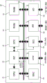
Fig. 1A is a block diagram showing a configuration of a microcomputer according to an implementation example. A microcomputer (microcontroller unit: hereinafter referred to as MCU)10 is a semiconductor device corresponding to SD in fig. 13 and including the functional blocks or modules shown in fig. 1A over one semiconductor substrate. That is, the MCU 10 includes a central processing unit (hereinafter referred to as CPU)11, a data transfer device (data transfer controller: hereinafter referred to as DTC)12, an interrupt controller (INT)13, a read only memory (hereinafter referred to as ROM)14, and a random access memory (hereinafter referred to as RAM) 15. The MCU 10 further includes a bus controller (hereinafter, referred to as BSC)16, a TIMER (TIMER)17, an SCI (serial communication interface) 18 corresponding to the SI in fig. 13, an ANALOG module (ANALOG)19 such as an a/D (ANALOG/digital) converter and a D/a (digital/ANALOG) converter, an input/output port (I/O) 1A.
The CPU 11 serving as an operation core in the MCU 10 operates by reading instructions mainly from the ROM 14. The ROM 14 includes a nonvolatile memory such as a flash memory as an electrically erasable memory. The DTC12 performs data transfer instead of the CPU 11 based on the setting made by the CPU 11.
The INT 13 receives an interrupt request (INTREQ) from the BSC 16, the timer 17, the SCI 18, and the analog block 19 and an interrupt request (INTREQ) from the I/O1A based on an external interrupt request signal from outside the MCU 10, and outputs the interrupt request to the CPU 11 or the data transfer start request to the DTC 12. When the processing due to the interrupt signal is started or when the processing is completed, the interrupt signal or the interrupt factor flag corresponding to each of the BSC 16, the timer 17, the SCI 18, the analog block 19, and the I/O1A is output as an interrupt clear signal (INTCLR) for clearing the interrupt.
The BSC 16 receives bus request signals from the CPU 11 and the DTC12, arbitrates occupation of the MCU internal bus 1B, and outputs a bus use enable signal. The BSC 16 associates bus requests, bus responses, bus commands, waits, addresses, data, and the like with the CPU 11 and DTC12, and implements reading/writing of the RAM15 and other functional blocks or modules attached to the MCU internal bus 1B. The RAM15 includes a volatile memory such as an SRAM.
The transmit data output (TXD) and receive data input (RXD) of the SCI 18 are output and input via the external SCI of the MCU 10 and the serial bus. At this time, output and input may be performed via the input/output port if necessary.
Fig. 1B is a block diagram illustrating a host interface of the microcomputer illustrated in fig. 1A. The SCI 18 activates the DTC12 with the INT 13 using a DTC activation request (dtreq). The data transfer start factors of SCI 18 include a command reception complete (command reception data full) interrupt request (CRXI), a data reception complete (reception data full) interrupt request (DXI), and a data transmission complete (transmission data empty) interrupt request (TXI).
The DTC12 reads data transfer information corresponding to the number of DTC vectors (DTCVEC) indicated by the INT 13 from the RAM15, and performs data transfer. Data transfer information corresponding to the data transfer start factor is provided. As described later, the data transfer information to be used in the reception data full (reception data transfer) and the transmission data empty (transmission data transfer) is switched by the data transfer corresponding to the command reception completion. The DTC12 activates an acknowledgement signal (ACK) at the time of data transfer and outputs a mode control signal (MDC) according to the data transfer information or the transferred data. The response signal (ACK) and the mode control signal (MDC) are supplied to the SCI 18 via the INT 13, and based on this, the mode controller (SCIMDC) of the SCI 18 performs a mode change which will be described later, the SIMDC corresponding to the MDCC in fig. 13. The SCI 18 outputs a Status (ST) according to the mode and status of transmission and reception.
The SCI 18 and the data transfer device may be directly coupled when uniquely determining the start factor of the data transfer device. This can be understood as combining the DTC12 and INT 13 as a data transfer device.
(SCI)
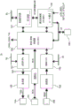
Fig. 2 is a block diagram illustrating the construction of the SCI illustrated in fig. 1A. The SCI 18 includes a control REGISTER 181 corresponding to REGISTER in fig. 13, a mode controller (SCIMDC)182 corresponding to MDCC in fig. 13, a transmission-reception controller (SCICNT)183, a receiver 184, a transmitter 185, a reception FIFO 186, and a transmission FIFO 187.
The control registers 181 include a mode register (SMR), a control register (SCR), a status register (SSR), and a function control register (SFCR) to specify a system and a format of transmission and reception and to display a status of an interrupt request. For example, the operation enable state of SCI 18 (SCI enabled) is specified corresponding to a case where the Transmit Enable (TE) bit or Receive Enable (RE) bit of the SCR is set to 1. This operation enable state is specified after specifying another transmission and reception system and format. In other words, in the operation enabled state, the system and format of transmission and reception are not changed.
In the transmission operation, when the Synchronous Clock (SCK) is input in a state where valid data exists in the transmission FIFO 187, transmission data (TXD) is output to the output terminal 18A by the transmitter 185. When the Synchronous Clock (SCK) is input in a state where valid data does not exist in the transmission FIFO 187, a transmission overrun error occurs.
In the receiving operation, reception data (RXD) is input from the input terminal 18B to the receiver 184 in synchronization with the Synchronous Clock (SCK). When a unit of data is input, the data is transferred to the reception FIFO 186. When the reception data is further input in a state where the reception FIFO 186 is full, a reception overrun error occurs.
In the operation enable state in which the TE bit and the RE bit are set to 1 in the control register 181, the transmission operation and the reception operation are simultaneously performed because the Synchronous Clock (SCK) is common to transmission and reception. This operation enable state is referred to as a simultaneous transmit-receive operation enable state. Even in the simultaneous transmission-reception operation enabled state, when a transmission overrun error or a reception overrun error occurs, the transmission-reception operation is not performed.
In the case of command reception (CMD ═ 1) in the simultaneous transmission-reception operation enabled state, SCICNT 183 does not generate a transmission overrun error and performs a transmission operation even if there is no valid data in transmission FIFO 187, and SCICNT 183 performs a transmission operation even if there is valid data in transmission FIFO 187, thereby holding transmission FIFO 187. In the present transmission operation, the transmission output is fixed to 0 or 1. This is the same operation as the case where the TE bit is set to 0. SCICNT 183 generates a command reception completion interrupt request (CRXI) upon receiving a data unit.
In addition, in the simultaneous transmission-reception operation enabled state, the operation in the case of transmission refraining (TD ═ 1) is the same as that in the case of command reception.
In addition, in the simultaneous transmit-receive operation enabled state, SCICNT 183 ignores the receive data and holds receive FIFO 186 in the case of the receive refrain (RD ═ 1). Therefore, reception data full and reception overrun errors are not generated. This operation is the same as the case where the RE bit is set to 0.
The receiver 184 is coupled to the input terminal 18B, and stores reception data (RXD) on a bit-by-bit basis. When reception of a predetermined amount of data (for example, 8 bits) is completed, the data is transferred to the reception FIFO 186. When the RD bit to be described later is set to 1, this is not regarded as reception completion. The contents of the reception FIFO 186 can be read from the CPU 11 or the DTC12 via the MCU internal bus 1B.
The transmission data is written into the transmission FIFO 187 by the CPU 11 or the DTC12 via the MCU internal bus 1B. When a TDRE flag, which will be described later, is cleared and transmission is started, the contents of the transmission FIFO 187 are transferred to the transmitter 185. Transmitter 185 is coupled to output terminal 18A and outputs transmit data (TXD) on a bit-by-bit basis.
The Baud Rate Generator (BRG)188 is configured to generate timing that serves as a basis for transmission and reception. The Baud Rate Generator (BRG)188 is provided with a bit rate register and a bit rate counter.
FIG. 3 illustrates the register structure of the SCI shown in FIG. 1A. Fig. 3 shows only the bits associated with the clock synchronization pattern. Start-stop synchronization mode or other systems may also be implemented by employing control bits and status flags (not shown).
Depending on the system to which the MCU 10 is applied, the operation of the SCI 18 is fixed as: one of a transmission-only operation (TE ═ 1, RE ═ 0), a reception-only operation (TE ═ 0, RE ═ 1), and a simultaneous transmission-reception operation (TE ═ RE ═ 1). When the transmission and reception control manages the transition of the communication state, the register and the bit must be changed for representation in accordance with three operations of the transmission-only operation, the reception-only operation, and the simultaneous transmission-reception operation. To prevent a mismatch from being generated during communication operations such as transmission and reception operations, the TE bit and the RE bit are prohibited from being changed during the communication operations. After setting the TE and RE bits, the time required to synchronize the base clock through the Bode Rate Generator (BRG)188 must be waited for.
TXI occurs when both the TDRE flag and the TIE bit are set to 1. When both the RDRF flag and the RIE bit are set to 1, CRXI or DRXI occurs due to the CMD bit to be described later. ERI occurs when both the OREG flag and the RIE bit are set to 1.
The CMD bit, TD bit, and RD bit are changed according to SCIMDC 182 in response to the mode control signal (MDC) from DTC 12.
Fig. 4 illustrates mode control state transitions of the SCI illustrated in fig. 1A. After the reset, the state is a stop state ST1 in which the TE bit and the RE bit are set to 0. When the SCR of the control register 181 is set and at least one of the TE and RE bits is set to 1 by the CPU 11, the state is set to the operation enable state ST 2. The operation enable state ST2 is one of a transmission operation (TE ═ 1), a reception operation (RE ═ 1), and a transmission-reception operation (TE ═ RE ═ 1).
First, although not particularly limited by the SFCR setting (mode control) performed by the DTC operation, the CMD bit is set to 1 for transitioning the state to the command reception state ST 21. When the command reception is completed, the state transitions to the setting determination/wait state ST22, waiting for the DTC12 to perform the mode control.
This mode control transits to one state among the data reception state ST23, the data transmission-reception state ST24, and the data transmission state ST 25. The transition to the data reception state ST23 is made when the TD bit is set to 1, the transition to the data transmission state ST25 is made when the RD bit is set to 1, and the transition to the data transmission-reception state ST24 is made when neither the TD bit nor the RD bit is set to 1 (both are cleared). When the required data reception, data transmission and reception, or data transmission is performed, the state transitions to the setting determination/wait state ST26, waiting for the DTC12 to perform the mode control. With the mode control, the CMD bit is set to 1, thereby transitioning to the command receiving state ST 21. In the operation enable state ST2, the system and format of transmission and reception are unchanged.
(INT)
Fig. 5 is a block diagram illustrating the configuration of the interrupt controller (INT) illustrated in fig. 1A. There are two interrupt factors for the MCU 10, internal and external interrupts, each interrupt being provided with an interrupt factor flag. Here, only the internal interrupt factor from SCI 18 is typically shown.
As in the case of the SCI 18, the interrupt factor flag is set to 1 when the function blocks of the timer 17 and the analog block 19 become a predetermined state, or when the external interrupt input terminal of the MCU 10 becomes a predetermined state. An interrupt request is issued to the INT 13 when the interrupt factor flag is set to 1 and the corresponding interrupt enable bit is set to 1.
This interrupt request (INTREQ) is input to the interrupt/DTC determination circuit 131. The contents of the DTC enable register (DTER)132 are also input to the interrupt/DTC determination circuit 131. When an interrupt is requested, the interrupt/DTC determination circuit 131 selects whether to activate the DTC12 or to allow an interrupt of the CPU 11. When the DTE bit corresponding to the interrupt factor relating to the DTC enable register 132 is set to 1, the interrupt/DTC determination circuit 131 requests activation of the DTC12 and does not request an interrupt of the CPU 11. When the DTE bit of the DTC enable register 132 is cleared, the interrupt/DTC determination circuit 131 requests an interrupt of the CPU 11 without requesting activation of the DTC 12.
The interrupt/DTC determination circuit 131 outputs an interrupt request to the CPU 11 to the priority and mask determination circuit 133 and outputs an activation request to the DTC12 to the priority determination circuit 134, separately or independently. The priority and mask determination circuit 133 of the CPU is controlled according to a priority register, an interrupt mask level, and the like.
The priority and mask determination circuit 133 and the priority determination circuit 134 determine the priority when a plurality of interrupt requests have occurred in the interrupt request to the CPU 11 and the activation request to the DTC12, respectively. As a result of this determination, the highest priority is selected and the number of vectors is generated. The priority and mask determination circuit 133 outputs a CPU interrupt request (CPU int) and a vector number (VEC), and the priority determination circuit 134 outputs a DTC activation request (dtreq) and a DTC vector number (DTCVEC).
A DTC activation request (dtreq) is input to the DTC12, and a DTC vector number (DTCVEC) is input to the latch circuit 135. A DTC operation start signal (DTCSTA) and a DTC operation end signal (DTCEND) are output from the DTC12 and input to the latch circuit 135. That is, when the DTC12 starts operating, the DTC operation start signal (DTCSTA) becomes active and the latch circuit 135 latches and holds the DTC vector number (DTCVEC). When the data transfer of the DTC12 is completed, a DTC operation end signal (DTC end) becomes active and the latch of the latch circuit 135 is released.
The number of DTC vectors (DTCVEC) and the DTC operation end signal (dtend) are input to the decoder circuit 136, and the interrupt factor clear signal (INTCLR) or the DTE clear signal (DTECLR) from the DTC12 becomes an active state corresponding to the interrupt factor flag (e.g., TDRE, RDRF, and ORER of SCI 18), and the interrupt factor flag or DTE bit is cleared.
When the DTC12 is activated by a necessary interrupt factor, the CPU 11 writes data transfer information to a necessary address of the RAM15 in advance, and sets interrupt enable bits (for example, TIE and RIE of the SCI 18) of the relevant interrupt and DTE bits corresponding to the relevant interrupt factor of the DTC enable register 132 to 1.
When the relevant interruption factor flag is set to 1 in this state, the DTC12 is activated. In a state where the DTC12 is performing an operation such as a predetermined data transfer, the DTC12 clears an interrupt factor flag concerned for each data transfer by an interrupt factor clear signal (INTCLR). At this time, an interrupt of the CPU 11 is not requested.
When the predetermined data transfer is completed, the DTC12 clears the DTE bit at the end of the operation by using a DTE clear signal (DTECLR). At this point, the relevant interrupt factor flag is held at 1 and the DTE bit is cleared. Thus, an interrupt of the CPU 11 is requested. The CPU 11 executes processing corresponding to the end of a predetermined data transfer or the like, and resets data transfer information or a DTE bit.
(DTC)
Fig. 6 shows data transmission information (transmission information group) of the DTC shown in fig. 1A. The data transfer information of the DTC12 includes a Mode Register (MR), a Data Register (DR), first and second source (transfer source) address registers (SAR1, SAR2), a destination (transfer Destination) Address Register (DAR), and a transfer Count Register (CR).
The necessary one of these registers is used, depending on what is held in the MR. The CR is divided into a Block Transfer Count Register (BTCR) and a Transfer Count Register (TCR). The TCR is divided into high order 8 bits (TCRH) and low order 8 bits (TCRL). The operation is performed according to a data transfer mode which will be described later. As for these registers (MR, CR), there are a set of circuits in the DTC12, and although not particularly limited, they do not exist in the address space of the CPU 11. The necessary number of sets of data transfer information to be stored in these registers are arranged in a predetermined data transfer information address area of the RAM15 on the address space of the CPU 11, for example.
The bits of the Mode Register (MR) are constructed as follows. Bits 31-36 specify the setting of the data transfer mode and the input data for table reference. Bit 15-0 specifies the table reference for the data transfer function and also specifies the data transfer for the normal data transfer function.
Bit 27 is an MDCE bit. The DTC12 performs data transfer CR to 0 in a state where the MDCE bit is set to 1, and outputs a mode control signal (MDC).
Bits 26-24 are MDC [2:0] bits. In a state where the TLU bit is cleared and the MDCE bit is set to 1, the mode control signal (MDC) is specified when the data transfer CR is 0. In this case, the MDC [2] bit is reflected to the CMD bit, the MDC [1] bit is reflected to the TD bit, and the MDC [0] bit is reflected to the RD bit. In a state where both the TLU bit and the MDCE bit are set to 1, the DTC12 outputs a mode control signal (MDC) based on data read from a table specified by the SAR 2.
Bits 22-20 are SF [2:0] bits and specify that the input data is shifted left by 8-0 bits.
Bit 9 is a DIR bit for selecting which of the transfer source or transfer destination is a repetition area and a block area.
For a start factor, bit 1 is the NXTE1 bit that selects whether to terminate the data transfer or perform the next data transfer. When the NXTE1 bit is cleared, after the data transfer information is read and the data is transferred, the data transfer information is written and the operation of the DTC is terminated. When the NXTE1 bit is set to 1, after the data transfer information is read and the data is transferred, the data transfer information is written. Further, the data transfer information is read from the consecutive addresses, the data transfer specified by the current data transfer information is performed, and the data transfer information is written. This operation is called chain transfer. Bit 0 is the NXTE0 bit that specifies whether to perform a chain transfer when CR becomes 0.
Fig. 7 is a block diagram illustrating the configuration of the DTC illustrated in fig. 1A. The DTC12 includes a data transfer control block (dtcnt) 121, a Bus Interface (BIF)122, a vector generation block (VG)123, a Vector Address Register (VAR)124, and an Arithmetic Logic Unit (ALU) 12A. The DTC12 also includes a Mode Register (MR), a first source address register (SAR1), a second source address register (SAR2), a Destination Address Register (DAR), and a data transfer Counter (CR).
The DTCC 121 controls the DTC12 based on the DTC activation request (DTCRQ) from the INT 13 and the content of the MR.
The MR, SAR1, SAR2, DAR, and CR store data transfer information sequentially read from the region of the RAM15 indicated by the leading address of the data transfer information stored in the VAR 124.
The ALU 124 has functions such as logical operations, shifts, and arithmetic operations, and performs two or more of these operations in a given order.
Although not shown, the DTC internal bus 12B has multiple buses, enabling the contents of SAR1, SAR2, DAR, and CR to be supplied to ALU 12A for operation. According to this configuration, an operation in the repeat mode or the block transfer mode is performed. The contents of the data transfer operation in the repeat mode and the block transfer mode can be realized by employing a well-known technique. Therefore, a detailed description thereof will be omitted.
When a DTC activation request signal (dtreq) is supplied from the INT 13, the DTC12 starts operating. When the DTC12 starts operating, the dtcc 121 sets a DTC operation start signal (DTCSTA) to an active state. When data transfer is performed, the dtcnt 121 activates an acknowledge signal (ACK) in synchronization with this bus cycle. When the transfer Counter (CR) is 0 and according to the setting of the MR, the dtcnt 121 changes the mode control signal (MDC) to a predetermined state and sets the SFCR of the SCI 18. The dtcnt 121 activates an interrupt factor clear signal (INTCLR) or a DTE clear signal (DTECLR), clears an interrupt factor flag or DTE bit serving as a start factor, and terminates an operation. After the DTC12 terminates the operation, the dtcc 121 activates a DTC operation end signal (DTC end) and returns to a stop state.
< application >
Fig. 8A is a block diagram showing a configuration of a microcomputer system according to an application. Fig. 8B is a block diagram illustrating a connection relationship of the microcomputer system illustrated in fig. 8A. The microcomputer system 1 includes a master MCU 10M, a slave MCU 10S, a motor 20, and an encoder 30 for detecting the position of the motor 20. The microcomputer system 1 is, for example, a camera system, and the host MCU 10M is a camera body MCU and the host MCU 10S is a camera lens MCU.
The MCU 10 according to the implementation example is applied to the master MCU 10M and the slave MCU 10S. The slave MCU 10S uses a timer 17F for driving of the focus motor (M), a timer 17D for input of an ENCODER (ENCODER) for detecting the position of the focus motor 20, and a timer 171 with an interval timer function. The SWITCH (SWITCH) of various types of settings is input via, for example, an output port (I/O) 1A.
As shown in FIG. 8B, the SCI 18 of the master MCU 10M and the SCI 18 of the slave MCU 10S are associated with each other with three signal lines of the clock synchronization mode and one signal line of the input/output port indicating the status. A terminal 18A for outputting TXD, a terminal 18B for inputting RXD, a terminal 18C for outputting SCK, and a terminal 18D for inputting ST of the master MCU 10M are coupled to the terminal 18D for inputting RXD, the terminal 18A for outputting TXD, the terminal 18C for inputting SCK, and the terminal 18D for outputting ST of the slave MCU 10S, respectively. The master MCU 10M outputs the Synchronous Clock (SCK), and the slave MCU 10S outputs the Status (ST).
(first example of communication operation)
Fig. 9 is a timing chart showing a first example of a communication operation in the microcomputer system shown in fig. 8A. A first example of a communication operation is the case of master transmission/slave reception. In FIG. 9, the shaded portion shows the operation of the DTC12 performing mode control of the SCI 18 of the slave MCU 10S.
First, the master MCU 10M and the slave MCU 10S perform initial settings on the registers of the respective SCIs 18 as transmission-reception operations (TE ═ 1, RE ═ 1) (timing T1).
The master MCU 10M inputs the State (ST) output of the slave MCU 10S. When the State (ST) is BUSY (BUSY) state, transmission is on standby. When the transmission data (command) is set and the Status (ST) input becomes the standby (READY) state, the master MCU 10M transmits the Command (CMND). At this time, the host MCU 10M sets the RD bit to 1, ignoring the reception data.
The slave MCU 10S sets the CMD bit to 1 and sets the TD bit to 1 to set command reception (time T1). The setting of the transmission data air-break request (TXI) is inhibited, the data setting for the transmission FIFO 187 is not performed, the transmission data (TXD) is fixed at, for example, a high level, and Dummy (DUMY) data is output. When reception begins, the Status (ST) output is set to busy. When the reception of the command is completed, the SCI 18 issues a command reception completion interrupt request (CRXI), and the INT 13 issues a DTC activation request (dtreq) to the DTC 12. The DTC12 reads the received data of the command, adds this to the SAR2, and reads the table area of the RAM 15. These contents set the DTC vector (TXI vector, DRXI vector) of the transmission data empty (transmission data transfer) and data transfer start request designated by the DAR due to the reception data being full (reception data transfer). In the present embodiment, it is assumed that two long words are block transferred. When one of the two long words is predetermined data (e.g., when it is 00000000), a mode control signal (MDC) is activated to set the corresponding TD bit or RD bit to 1. Specifically, when the DTC vector for which transmission data is empty is 00000000, the TD bit is set to 1 to enable transmission refraining. When the DTC vector for which reception data is full is 00000000, the RD bit is set to 1 to enable reception refraining. The CMD bit is cleared. Following this mode control signal (MDC), the SCI 18 sets the SRCR, switches to data reception or data transmission, and sets the Status (ST) output to busy. In this case, corresponding to the above-described command, there are three modes: master transmission/slave reception, slave transmission/master reception, and master/slave transmission and reception. The present embodiment takes the case of master transmission/slave reception as an example. Therefore, the master sets the RD bit to 1 to enable the reception inhibition (data transmission), and the slave sets the TD bit to 1 to enable the transmission inhibition (data reception) (time T2).
In the master MCU 10M, after completion of the command transmission itself, transmission data is set. When the State (ST) input becomes the standby state, a predetermined amount of data corresponding to the command is transmitted.
The slave MCU 10S sets the Status (ST) output to busy at the start of data reception. Following completion of data reception, a reception data full (reception data transfer) data transfer start request is issued from the MCU 10S to activate the DTC 12. The DTC12 transfers the received data to a predetermined address of the RAM 15. A predetermined amount of data corresponding to the command is set to CR, and the amount of data according to this is transmitted. When CR becomes 0, the mode control signal (MDC) specified by MR is output, and the mode control state of SCI 18 transitions (time T3). Accordingly, SCI 18 sets the Status (ST) output to standby. When CR completes the data transfer of 0, an interrupt request is issued to the CPU 11.
Fig. 10 shows data transfer for command reception completion in the first example of fig. 9. In the data transfer for completion of the command reception in the MCU 10S, the CPU 11 sets data transfer information as follows.
In the MR, the TLU bit, the BRM bit, and the MDCE bit are all set to 1. The SF [2:0] bit specifies + 4. The ISz [1:0] bits specify the byte size corresponding to the command. The SM1 bit and SM0 bit specify SAR2 is fixed. DM1 bit and DM0 bit specify DAR fix. The TMD1 bit and the TMD0 bit specify the normal mode. SAR1 specifies the address of receive FIFO 186. SAR2 specifies the first address of the table region of the DTC vector for data transmission empty transfer requests and data reception full transfer requests. The DAR specifies the DTC vector address of data transmission empty transfer requests and data reception full transfer requests. These information items are stored as data transfer information C shown in fig. 10.
In fig. 10, thin-line arrows indicate the description of addresses, and double-line arrows indicate reading/writing of data.
(A) When the DTC is activated due to completion of command reception, the first address of the data transfer information is read from the corresponding vector area (CRXI vector) specified by the vector address of the CRXI interrupt).
(B) Based on this address, the data transfer information C is read from the data transfer information address area. This data transfer information C is the content to be stored in MR, SAR1, SAR2 and DAR. The address of receive FIFO 186 is stored in SAR 1. The first address of the table region is stored in SAR 2. The TXI vector address is stored in the DAR.
(C) First, a command of a specified byte size in ISz bits is read from the reception FIFO 186 specified by SAR 1. The read data is left shifted by ALU 12A by 4 bits specified in the SF [2:0] bits. This result is added to SAR2 and used as the source address.
(D) The transmitted data is read from the source address of the table region specified by SAR 2. In this embodiment, the TXI vector n and the DRXI vector n are read.
(E) This is written into the TXI vector region and the DRXI vector region specified by the DAR. At the same time, the mode control signal (MDC) is output as described above. For example, the DRXI vector n is content indicating necessary data transfer information m.
Accordingly, data transfer information corresponding to the command and in response to TXI and DRXI data transfers may be selected (from data transfer information m, m1, m2, m3, etc.).
In the case of the byte size, the command can be specified among 256 kinds at most. The command may define the presence or absence of subsequent data, the length of the data, and the kind of data. For example, a command involves writing subsequent data to the timers 17D, 17F and 17I and the I/O port 1A of the slave MCU 10S, and another command involves transmitting desired data of the timers 17D, 17F and 17I and the I/O port 1A of the slave MCU 10S. This command can be arbitrarily defined according to a command suitable for the microcomputer system 1 concerned.
Fig. 11 shows data transfer for reception data full (reception data transfer) in the first example of fig. 9. In data transfer (reception data transfer) full for reception data in the MCU 10S, data transfer information is set as follows.
In MR, the TLU bit and the BRM bit are cleared and the MDCE bit is set to 1. The Sz [1:0] bits specify the byte size corresponding to the command. The SM1 bits and SM0 bits specify SAR fixation. The DM1 bit and DM0 bit specify DAR increments. The TMD1 bit and the TMD0 bit specify the normal mode. SAR specifies the address of receive FIFO 186. The DAR specifies the address of the RAM15 for data reception. The CR specifies the amount of data corresponding to the command. These information items are stored as data transfer information m shown in fig. 11.
(A) When the DTC12 is activated due to reception data being full (reception data transfer), the head address of the data transfer information is read from the corresponding vector area (DRXI vector) specified by the vector address of the DRXI break). Since the command reception is completed, it is updated to necessary contents by data transfer, and it indicates the data transfer information m.
(B) Based on this address, the data transfer information m is read from the data transfer information address area. This data transfer information is the contents of the MR, SAR, DAR, and CR. The address of the receive FIFO 186 is stored in SAR and the address of RAM15 is stored in DAR.
(C) First, received data of the byte size specified by the Sz bit is read from the reception FIFO 186 specified by the SAR. The read reception data is written in the RAM15 designated by the DAR. This operation is repeated as many times as specified by CR. When CR becomes 0, the mode control signal (MDC) is output as described above.
(second example of communication operation)
Fig. 12 is a timing chart showing a second example of a communication operation in the microcomputer system shown in fig. 8A. In a second example of the communication operation, the data transfer corresponding to the command is a slave send/master receive. As in the case of the first example described above, the master MCU 10M and the slave MCU 10S respectively perform initial settings as transmission-reception operations, and perform transmission and reception of commands.
In order to output the synchronous clock corresponding to the number of necessary data, the master MCU 10M sets the TD bit to 1, and transmits dummy data by, for example, fixing the transmission data to a high level.
By performing mode control of the DTC12 when the command reception is completed, the slave MCU 10S sets the RD bit to 1 to validate data transmission (time T2). That is, the DTC vector on the table of the RAM15 whose transmission data is empty is set to a predetermined vector other than 00000000, and the DTC vector whose reception data is full is set to 00000000.
In order to transmit a predetermined amount of data corresponding to the command, the slave MCU 10S activates the DTC 12S according to a transmission data null (transmission data transfer) data transfer request. The DTC12 transmits data to be transmitted from a predetermined address of the RAM15 to the transmission FIFO 187. The DTC12 sets the Status (ST) output to busy at the beginning of data transmission. A predetermined number of data transfers indicated by the CR are performed. When CR becomes 0, the mode control signal (MDC) specified by MR is output, and the mode control state of the SCI 18S transitions (time T3'). At this time, the change of the mode or the change of the SFCR is not reflected immediately, but is reflected (time T3) after the output of the transmission data is completed (in a state where the data has been exhausted in the transmission FIFO 187 and the transmitter 185). In other words, the reflection is enabled after the mode control input is synchronized with the transmission and reception. The SCI 18S sets the Status (ST) output to standby. When the CR completes the data transfer of 0, the SCI 18S requests an interrupt to the CPU 11.
In data transfer (send data transfer) in which the send data is empty, data transfer information is set as follows.
In MR, the TLU bit and the BRM bit are cleared and the MDCE bit is set to 1. The Sz [1:0] bits specify the byte size corresponding to the command. The SM1 bits and SM0 bits specify SAR increments. DM1 bit and DM0 bit specify DAR fix. The TMD1 bit and the TMD0 bit specify the normal mode. The SAR specifies the address of the RAM 15S to which data is transmitted. The DAR specifies the address of transmit FIFO 187. The CR specifies the amount of data corresponding to the command.
(third example of communication operation)
In the case of master/slave transmission and reception as a third example of a communication operation, although not shown, the slave MCU 10S clears both the TD bit and the RD bit, and the DTC12 does not control a change of the SFCR at the time of data transfer due to completion of transmission data but controls a change of the SFCR at the time of data transfer due to completion of reception data. That is, the DTC vector whose transmission data is empty and the DTC vector whose reception data is full on the table of the RAM15 are set to predetermined vectors other than 00000000.
According to the above implementation example, the following operational effects are obtained.
(1) By setting the TD bit or the RD bit to 1 in a state where transmission and reception are enabled (TE ═ RE ═ 1) (the simultaneous transmission-reception operation remains specified), the operation of transmission or reception can be inhibited. In the case of the transmission operation refraining, preparation of transmission data and description of transmission start are not required, and it becomes possible to perform transmission and reception operations of arbitrary data corresponding to the synchronous clock input. In the case of the reception operation refraining, the received content is ignored, no overrun error is detected, and no interrupt request and data transfer start request are made. Therefore, in the operation enable state of the simultaneous transmission-reception operation and the synchronous clock input, it becomes possible to temporarily perform the transmission operation refraining and the reception operation refraining, in other words, the standby time for changing the setting is not required. Unnecessary to prepare useless transmission data and process useless reception data; therefore, the efficiency of the process can be enhanced. If either the TE bit or the RE bit is switched, it must be ensured that it is consistent with the operation of the entire SCI. In contrast, by limiting the control targets of the TD bit and the RD bit without changing the basic operation of the simultaneous transmission-reception operation, the logic can be simplified. The likelihood of falling into an undesired state may be reduced.
(2) In the receiving operation, whether the operation is to receive a command or data may be specified, and the operations may issue an interrupt request or a data transfer start request, respectively. Thus, it becomes possible to generate the start factor of the data transfer apparatus in a dedicated manner. When the command reception operation is performed, it is not necessary to prepare transmission data by specifying the transmission operation prohibition. At the time of data reception operation, transmission operation refraining may be designated. Since the interrupt request for command reception completion and the interrupt request for data reception completion are separated, it is possible to immediately and directly process without determining which interrupt request is. It is possible to efficiently select an appropriate processing method such that data transfer by the data transfer apparatus is performed in response to an interrupt request for command reception completion, and interrupt processing by the CPU is performed in response to an interrupt request for data reception completion.
(3) The mode is switched according to an operation of the data transfer apparatus in response to a start factor and modes such as command reception, data-only reception, and data-only transmission. For example, when data transfer by the data transfer device in response to data transmission or data reception is completed, the mode is switched to command reception.
(4) A state corresponding to the mode may be output. By specifying the receiving operation in the state of command reception, the state output to the outside is set to the second state (busy state). When the mode is changed by an operation of the data transfer device in response to completion of reception of the command, the state output to the outside is set to the first state (standby state). The status output is set to the first state (standby) when the status output is set to the second state (busy state) by the data transmission operation or the data reception operation and when the mode is switched (to command reception) by the above-described operation of the data transfer apparatus.
Therefore, a mode corresponding to actual communication processing can be realized, and setting change and standby time can be reduced. By activating the data transfer device according to the mode and the communication operation, and switching the mode by the control of the data transfer device, the processing of the CPU becomes unnecessary and improvement and acceleration of efficiency can be achieved. By enabling the data transfer device to perform mode control of SCI, judgment of command, and data transfer instead of the CPU, the frequency of issuing interrupt requests to the CPU can be reduced and the period of time during which the CPU operates in a low power consumption state can be extended. It is possible to eliminate the exceptional processing, the stack evacuation/return operation, and the execution of the return instruction that the CPU should execute in the interrupt processing, thereby contributing to simplification of the program or improvement of the efficiency of the system. It is also possible to shorten the time from the occurrence of an event to the execution of a necessary operation and to enhance so-called responsiveness. By the operation of the data transfer apparatus which has a smaller logic size than the CPU and can perform high-speed processing, and by causing the CPU to operate in a low power consumption state, low power consumption can be achieved. The development efficiency of the software can also be enhanced.
It is possible to flexibly support a command and communication system suitable for each of microcomputer systems. When expressed in other languages, the mode of transmission and reception of the microcomputer can be changed according to data supplied to the microcomputer.
As described above, the invention achieved by the inventors of the present invention has been described based on the embodiments, implementation examples, and application specific. It should not be emphasized too strongly, however, that the invention is limited to the embodiments, implementation examples and applications described above, which can be varied in various ways.
The following explanation is adopted as an example of this implementation: the TE bit and the RE bit are used as operation permission after SCI setting is completed, and the TD bit and the RD bit are separately provided. However, it is preferable that the operation enable bit of SCI is provided in common for transmission and reception, and the functions of the TE bit and the RE bit and the functions of the TD bit and the RD bit are combined so as to be able to be changed during operation. Although the transmission output may be arbitrary in the case of command reception and transmission refraining, it is desirable to fix it to 0 or 1. When the CMD bit is set to 1, it is also preferable to set a transmission refrain regardless of the TD bit. It is also preferable to not use a common RDRF flag as the interruption factor flag for CRXI and DRXI, but to use separate interruption factor flags. It is also preferred that the RIE bit or RDRF flag is cleared when the RD bit is set to 1. The long word data for specifying the TD bit and the RD bit may be data that is not used as the data transfer information storage area. This implementation example employs 00000000, which is the same as the reset vector of the CPU. This is based on the assumption that it is not used as a data transfer information storage area. The lower order 2 bits may be used when the data transfer memory address is considered to be in units of long words.
The amount and empty space of data of the reception FIFO and the transmission FIFO for detecting the reception data full (reception data transfer) and the transmission data empty (transmission data transfer) can be changed by using the control register. It is also preferable that a unit other than the byte size for determining the completion of reception in command reception can be selected. The data transfer information and the vector area may be rewritten according to the data transfer due to the completion of the command reception. Preferably, the CPU can set CMD bit, TD bit and RD bit. It is also preferable to make the CPU process an arbitrary command so as to set the CMD bit, TD bit, and RD bit.
The implementation example is illustrated by taking SCI as an example; however, the present invention is not limited thereto, and is applicable to serial communication interfaces such as I2C (inter integrated circuit) and SPI (serial peripheral interface). The implementation example is explained by taking DTC as an example; however, the present invention is not limited thereto, and is also applicable to, for example, DMACs (direct memory access controllers) that transfer data between memories and registers. The specific configuration of the DTC and interrupt controller may also be varied in various ways. The explanation of the details of the BSC and the bus operations such as bus right and wait are omitted; however, they may be implemented appropriately. The present invention may be applied to only one of the master MCU and the slave MCU. In this case, it is more preferable to apply to the slave MCU.
The configuration of the microcomputer is not limited. The functional blocks and others may be changed. The above description was made regarding the case where the present example is applied to a microcomputer; however, the present invention is not limited thereto, and the present invention may be applied to other semiconductor devices, for example, a Digital Signal Processor (DSP).
< illustrative examples >
Hereinafter, illustrative examples are described.
(additional appendix 1)
A semiconductor device includes an interface circuit for performing sequential communication of transmission or reception according to a synchronous clock.
In the semiconductor device, the interface circuit includes:
a first register for specifying an operation enable state as at least one of a transmission state and a reception state, an
A second register for holding information to specify transmission refraining or reception refraining; and
determining at least one operation of sending or receiving information based on the state of the first register and the state of the second register.
(additional appendix 2)
A system, the system comprising:
a first semiconductor device including a first interface circuit for performing sequential communication of transmission or reception according to a synchronous clock, an
A second semiconductor device including a second interface circuit for performing sequential communication of transmission or reception according to the synchronous clock.
In the system, the second interface circuit includes:
a first register for specifying an operation enable state as at least one of a transmission state and a reception state, an
A second register for holding information to specify transmission refraining or reception refraining, and
determining at least one operation of sending or receiving information based on the state of the first register and the state of the second register.
Claims (18)
1. A semiconductor device, the semiconductor device comprising:
an interface circuit operable to perform sequential communication of transmission or reception according to a synchronous clock,
wherein the interface circuit comprises:
a first register operable to specify an operation enable state that enables at least one of a transmit state and a receive state; and
a mode control circuit operable in the operation enable state to change at least one of transmission or reception according to the generated information to change the at least one mode of the interface circuit at the time of data transfer based on data transfer information or contents of the data transfer, and
wherein the mode control circuit changes between the following modes when in the operational enable state: a transmit and receive mode, a transmit mode, and a receive mode.
2. The semiconductor device according to claim 1,
the interface circuit outputs a state in response to the change in mode.
3. The semiconductor device according to claim 1, further comprising:
a second register operable to: in the transmission-reception state, information for specifying transmission refraining or reception refraining is held.
4. The semiconductor device according to claim 3,
the second register holds information capable of specifying one of command reception and data reception.
5. The semiconductor device according to claim 1, wherein the interface circuit can output one of:
the data transmission completes the interrupt request and,
command reception completes the interrupt request, an
The data reception completes the interrupt request.
6. The semiconductor device according to claim 1, further comprising:
a data transmission device for transmitting data to a data transmission device,
wherein the mode control circuit is controlled corresponding to a predetermined operation of the data transfer apparatus, and the mode control circuit is changed to the at least one mode after completion of a transmission operation or a reception operation, and
wherein at least the mode of transmitted and received data transfer is transitioned while in the transmit state or receive state.
7. The semiconductor device according to claim 5, further comprising:
a data transmission device for transmitting data to a data transmission device,
wherein the data transfer device is activated in response to one of the data transmission completion interrupt request, the command reception completion interrupt request, and the data reception completion interrupt request.
8. The semiconductor device as set forth in claim 7,
wherein the data transfer device comprises:
a register operable to store transfer mode information;
a register operable to store first source address information and second source address information;
a register operable to store destination address information; and
an arithmetic circuit, and
wherein the data transfer apparatus performs reading based on a result of arithmetic calculation performed by the arithmetic circuit on data read based on the first source address information and the second source address information, and performs writing based on the destination address information.
9. The semiconductor device according to claim 1, further comprising:
a central processing unit;
an interrupt control circuit; and
a data transmission device for transmitting data to a data transmission device,
wherein the interface circuit makes an interrupt request to the interrupt control circuit, an
Wherein, in response to the interrupt request, the interrupt control circuit outputs an interrupt signal to the central processing unit or outputs a start request to the data transfer apparatus.
10. A system, the system comprising:
a first semiconductor device comprising a first interface circuit operable to perform sequential communications of transmission or reception according to a synchronous clock; and
a second semiconductor device including a second interface circuit operable to perform sequential communication of transmission or reception according to the synchronous clock,
wherein the second interface circuit comprises:
a first register operable to specify a transmit state and/or a receive state; and
a mode control circuit operable in a transmit-receive state enabling transmission and/or reception, to change at least one of transmission or reception according to the generated information to change the at least one mode of the second interface circuit at the time of data transfer based on data transfer information or contents of the data transfer, and
wherein when the mode control circuit is in an operational enable state, changing between: a transmit and receive mode, a transmit mode, and a receive mode.
11. The system of claim 10, wherein the first and second light sources are arranged in a single package,
wherein the second interface circuit outputs a state in response to the change in mode, an
Wherein the first interface circuit inputs the state.
12. The system of claim 10, wherein the second interface circuit further comprises:
a second register operable to: in the transmission-reception state, information for specifying transmission refraining or reception refraining is held.
13. The system of claim 12, wherein,
the second register holds information capable of specifying one of command reception and data reception.
14. The system of claim 10, wherein,
the second interface circuit performs the sequential communication of transmission or reception in synchronization with one synchronous clock output from the first interface circuit.
15. The system of claim 10, wherein the first and second light sources are arranged in a single package,
wherein the second semiconductor device further comprises:
data transfer apparatus, and
wherein the mode control circuit is controlled corresponding to a predetermined operation of the data transfer apparatus, and changes the mode after completion of a transmission operation or a reception operation.
16. The system of claim 10, wherein the first and second light sources are arranged in a single package,
wherein the second semiconductor device further comprises:
data transfer apparatus, and
wherein the data transfer device is activated in response to one of a data sending completion interrupt request, a command receiving completion interrupt request, and a data receiving completion interrupt request, which are made by the second interface circuit.
17. The system of claim 16, wherein the first and second sensors are arranged in a single unit,
wherein the data transfer device comprises:
a register operable to store transfer mode information;
a register operable to store first source address information and second source address information;
a register operable to store destination address information; and
an arithmetic circuit, and
wherein the data transfer apparatus performs reading based on a result of arithmetic calculation performed by the arithmetic circuit on data read based on the first source address information and the second source address information, and performs writing based on the destination address information.
18. The system of claim 10, wherein the first and second light sources are arranged in a single package,
wherein the second semiconductor device further comprises:
a central processing unit;
an interrupt control circuit; and
a data transmission device for transmitting data to a data transmission device,
wherein the second interface circuit makes an interrupt request to the interrupt control circuit, an
Wherein the interrupt control circuit outputs an interrupt signal to the central processing unit or a start request to the data transfer apparatus in response to the interrupt request.
Applications Claiming Priority (2)
| Application Number | Priority Date | Filing Date | Title |
|---|---|---|---|
| JP2015141224A JP6602579B2 (en) | 2015-07-15 | 2015-07-15 | Semiconductor device and system |
| JP2015-141224 | 2015-07-15 |
Publications (2)
| Publication Number | Publication Date |
|---|---|
| CN106354674A CN106354674A (en) | 2017-01-25 |
| CN106354674B true CN106354674B (en) | 2021-05-07 |
Family
ID=57775925
Family Applications (1)
| Application Number | Title | Priority Date | Filing Date |
|---|---|---|---|
| CN201610478818.3A Active CN106354674B (en) | 2015-07-15 | 2016-06-27 | Semiconductor device and system |
Country Status (3)
| Country | Link |
|---|---|
| US (1) | US10409749B2 (en) |
| JP (1) | JP6602579B2 (en) |
| CN (1) | CN106354674B (en) |
Families Citing this family (6)
| Publication number | Priority date | Publication date | Assignee | Title |
|---|---|---|---|---|
| JP6786449B2 (en) * | 2017-06-29 | 2020-11-18 | ルネサスエレクトロニクス株式会社 | Semiconductor device |
| US10474822B2 (en) * | 2017-10-08 | 2019-11-12 | Qsigma, Inc. | Simultaneous multi-processor (SiMulPro) apparatus, simultaneous transmit and receive (STAR) apparatus, DRAM interface apparatus, and associated methods |
| US20210303496A1 (en) * | 2017-12-15 | 2021-09-30 | Hewlett-Packard Development Company, L.P. | Actuation of data transmission lanes between states |
| JP7172217B2 (en) * | 2018-07-17 | 2022-11-16 | 大日本印刷株式会社 | Secure element, communication method, communication program and communication system |
| CN110412913A (en) * | 2019-07-17 | 2019-11-05 | 江苏吉泰科电气股份有限公司 | Host computer switches DSP programming program control system online |
| JP7295780B2 (en) * | 2019-11-05 | 2023-06-21 | ルネサスエレクトロニクス株式会社 | Semiconductor device and method of operation thereof |
Family Cites Families (14)
| Publication number | Priority date | Publication date | Assignee | Title |
|---|---|---|---|---|
| JP2544385B2 (en) * | 1987-05-27 | 1996-10-16 | 株式会社日立製作所 | Communication control device |
| JP3019740B2 (en) * | 1994-12-27 | 2000-03-13 | 日本電気株式会社 | Serial interface and serial data transfer system |
| US5790895A (en) * | 1996-10-18 | 1998-08-04 | Compaq Computer Corporation | Modem sharing |
| US6381661B1 (en) * | 1999-05-28 | 2002-04-30 | 3Com Corporation | High throughput UART to DSP interface having Dual transmit and receive FIFO buffers to support data transfer between a host computer and an attached modem |
| KR100480084B1 (en) * | 2003-07-23 | 2005-04-06 | 엘지전자 주식회사 | A system for transmitting data using universal serial bus |
| JP4138693B2 (en) * | 2004-03-31 | 2008-08-27 | 株式会社東芝 | Flow control initialization method and information processing apparatus |
| DE102004057756B4 (en) * | 2004-11-30 | 2009-08-06 | Advanced Micro Devices Inc., Sunnyvale | USB control device with OTG control unit |
| JP5179834B2 (en) * | 2007-10-31 | 2013-04-10 | ルネサスエレクトロニクス株式会社 | Semiconductor device and data processing system |
| JP2010257280A (en) * | 2009-04-27 | 2010-11-11 | Renesas Electronics Corp | Serial control device, semiconductor device, and serial data transfer method |
| JP5414479B2 (en) | 2009-11-27 | 2014-02-12 | ルネサスエレクトロニクス株式会社 | Semiconductor device |
| US9296009B2 (en) * | 2012-07-13 | 2016-03-29 | Nordson Corporation | Adhesive dispensing system having metering system including variable frequency drive and closed-loop feedback control |
| US9059779B2 (en) * | 2012-11-27 | 2015-06-16 | Aviacomm Inc. | Serial digital interface between an RF transceiver and a baseband chip |
| JP6316593B2 (en) * | 2014-01-07 | 2018-04-25 | ルネサスエレクトロニクス株式会社 | Semiconductor device |
| JP6354387B2 (en) * | 2014-06-30 | 2018-07-11 | 富士通株式会社 | Information processing apparatus, information processing system, and interrupt apparatus control method |
-
2015
- 2015-07-15 JP JP2015141224A patent/JP6602579B2/en active Active
-
2016
- 2016-05-02 US US15/144,580 patent/US10409749B2/en active Active
- 2016-06-27 CN CN201610478818.3A patent/CN106354674B/en active Active
Also Published As
| Publication number | Publication date |
|---|---|
| JP2017021749A (en) | 2017-01-26 |
| US10409749B2 (en) | 2019-09-10 |
| JP6602579B2 (en) | 2019-11-06 |
| US20170019142A1 (en) | 2017-01-19 |
| CN106354674A (en) | 2017-01-25 |
Similar Documents
| Publication | Publication Date | Title |
|---|---|---|
| CN106354674B (en) | Semiconductor device and system | |
| JP2539614B2 (en) | Apparatus and method for generating pointer address | |
| US7529862B2 (en) | System for providing access of multiple data buffers to a data retaining and processing device | |
| US10482047B2 (en) | Slave device connected to master device via I2C bus and communication method thereof | |
| EP2097828B1 (en) | Dmac to handle transfers of unknown lengths | |
| US11341087B2 (en) | Single-chip multi-processor communication | |
| CN107810492B (en) | Configurable mailbox data buffer apparatus | |
| JP4903801B2 (en) | Subscriber interface connecting FlexRay communication module and FlexRay subscriber device, and method of transmitting message via subscriber interface connecting FlexRay communication module and FlexRay subscriber device | |
| JP2004326462A (en) | Multiprocessor system | |
| JP2006338538A (en) | Stream processor | |
| KR100708096B1 (en) | Bus system and execution scheduling method for access commands thereof | |
| US6330631B1 (en) | Data alignment between buses | |
| US8943238B2 (en) | Operations using direct memory access | |
| US7350015B2 (en) | Data transmission device | |
| JP2009163531A (en) | Interruption management mechanism and microcomputer | |
| KR20060004829A (en) | Direct memory access device, system and method for transmitting and receiving data through direct memory access device | |
| CN111177048A (en) | AHB bus equipment and data stream transmission method thereof | |
| CN110399322B (en) | Data transmission method and ping-pong DMA framework | |
| JPH1185673A (en) | Method and device for controlling shared bus | |
| CN115729863A (en) | Data transmission method, device, electronic equipment and medium | |
| JP4609540B2 (en) | Multi-processor system | |
| JP2667285B2 (en) | Interrupt control device | |
| JPH077954B2 (en) | Control device | |
| JPH06332842A (en) | Direct memory access control circuit | |
| JP2005182312A (en) | Device control circuit |
Legal Events
| Date | Code | Title | Description |
|---|---|---|---|
| C06 | Publication | ||
| PB01 | Publication | ||
| SE01 | Entry into force of request for substantive examination | ||
| SE01 | Entry into force of request for substantive examination | ||
| GR01 | Patent grant | ||
| GR01 | Patent grant |