JP6602579B2 - Semiconductor device and system - Google Patents
Semiconductor device and system Download PDFInfo
- Publication number
- JP6602579B2 JP6602579B2 JP2015141224A JP2015141224A JP6602579B2 JP 6602579 B2 JP6602579 B2 JP 6602579B2 JP 2015141224 A JP2015141224 A JP 2015141224A JP 2015141224 A JP2015141224 A JP 2015141224A JP 6602579 B2 JP6602579 B2 JP 6602579B2
- Authority
- JP
- Japan
- Prior art keywords
- reception
- transmission
- data
- mode
- data transfer
- Prior art date
- Legal status (The legal status is an assumption and is not a legal conclusion. Google has not performed a legal analysis and makes no representation as to the accuracy of the status listed.)
- Active
Links
Images


Classifications
-
- G—PHYSICS
- G06—COMPUTING; CALCULATING OR COUNTING
- G06F—ELECTRIC DIGITAL DATA PROCESSING
- G06F13/00—Interconnection of, or transfer of information or other signals between, memories, input/output devices or central processing units
- G06F13/38—Information transfer, e.g. on bus
- G06F13/42—Bus transfer protocol, e.g. handshake; Synchronisation
- G06F13/4282—Bus transfer protocol, e.g. handshake; Synchronisation on a serial bus, e.g. I2C bus, SPI bus
-
- G—PHYSICS
- G06—COMPUTING; CALCULATING OR COUNTING
- G06F—ELECTRIC DIGITAL DATA PROCESSING
- G06F13/00—Interconnection of, or transfer of information or other signals between, memories, input/output devices or central processing units
- G06F13/38—Information transfer, e.g. on bus
- G06F13/382—Information transfer, e.g. on bus using universal interface adapter
- G06F13/385—Information transfer, e.g. on bus using universal interface adapter for adaptation of a particular data processing system to different peripheral devices
-
- G—PHYSICS
- G06—COMPUTING; CALCULATING OR COUNTING
- G06F—ELECTRIC DIGITAL DATA PROCESSING
- G06F13/00—Interconnection of, or transfer of information or other signals between, memories, input/output devices or central processing units
- G06F13/38—Information transfer, e.g. on bus
- G06F13/40—Bus structure
- G06F13/4063—Device-to-bus coupling
- G06F13/4068—Electrical coupling
- G06F13/4072—Drivers or receivers
-
- G—PHYSICS
- G06—COMPUTING; CALCULATING OR COUNTING
- G06F—ELECTRIC DIGITAL DATA PROCESSING
- G06F13/00—Interconnection of, or transfer of information or other signals between, memories, input/output devices or central processing units
- G06F13/38—Information transfer, e.g. on bus
- G06F13/42—Bus transfer protocol, e.g. handshake; Synchronisation
- G06F13/4282—Bus transfer protocol, e.g. handshake; Synchronisation on a serial bus, e.g. I2C bus, SPI bus
- G06F13/4291—Bus transfer protocol, e.g. handshake; Synchronisation on a serial bus, e.g. I2C bus, SPI bus using a clocked protocol
-
- G—PHYSICS
- G06—COMPUTING; CALCULATING OR COUNTING
- G06F—ELECTRIC DIGITAL DATA PROCESSING
- G06F15/00—Digital computers in general; Data processing equipment in general
- G06F15/76—Architectures of general purpose stored program computers
- G06F15/80—Architectures of general purpose stored program computers comprising an array of processing units with common control, e.g. single instruction multiple data processors
- G06F15/8053—Vector processors
- G06F15/8076—Details on data register access
-
- H—ELECTRICITY
- H03—ELECTRONIC CIRCUITRY
- H03K—PULSE TECHNIQUE
- H03K19/00—Logic circuits, i.e. having at least two inputs acting on one output; Inverting circuits
- H03K19/0175—Coupling arrangements; Interface arrangements
- H03K19/017509—Interface arrangements
-
- H—ELECTRICITY
- H03—ELECTRONIC CIRCUITRY
- H03K—PULSE TECHNIQUE
- H03K23/00—Pulse counters comprising counting chains; Frequency dividers comprising counting chains
- H03K23/40—Gating or clocking signals applied to all stages, i.e. synchronous counters
- H03K23/50—Gating or clocking signals applied to all stages, i.e. synchronous counters using bi-stable regenerative trigger circuits
- H03K23/502—Gating or clocking signals applied to all stages, i.e. synchronous counters using bi-stable regenerative trigger circuits with a base or a radix other than a power of two
- H03K23/507—Gating or clocking signals applied to all stages, i.e. synchronous counters using bi-stable regenerative trigger circuits with a base or a radix other than a power of two with a base which is a non-integer
-
- H—ELECTRICITY
- H04—ELECTRIC COMMUNICATION TECHNIQUE
- H04B—TRANSMISSION
- H04B1/00—Details of transmission systems, not covered by a single one of groups H04B3/00 - H04B13/00; Details of transmission systems not characterised by the medium used for transmission
- H04B1/38—Transceivers, i.e. devices in which transmitter and receiver form a structural unit and in which at least one part is used for functions of transmitting and receiving
- H04B1/40—Circuits
- H04B1/401—Circuits for selecting or indicating operating mode
-
- H—ELECTRICITY
- H04—ELECTRIC COMMUNICATION TECHNIQUE
- H04B—TRANSMISSION
- H04B1/00—Details of transmission systems, not covered by a single one of groups H04B3/00 - H04B13/00; Details of transmission systems not characterised by the medium used for transmission
- H04B1/38—Transceivers, i.e. devices in which transmitter and receiver form a structural unit and in which at least one part is used for functions of transmitting and receiving
- H04B1/40—Circuits
- H04B1/44—Transmit/receive switching
-
- Y—GENERAL TAGGING OF NEW TECHNOLOGICAL DEVELOPMENTS; GENERAL TAGGING OF CROSS-SECTIONAL TECHNOLOGIES SPANNING OVER SEVERAL SECTIONS OF THE IPC; TECHNICAL SUBJECTS COVERED BY FORMER USPC CROSS-REFERENCE ART COLLECTIONS [XRACs] AND DIGESTS
- Y02—TECHNOLOGIES OR APPLICATIONS FOR MITIGATION OR ADAPTATION AGAINST CLIMATE CHANGE
- Y02D—CLIMATE CHANGE MITIGATION TECHNOLOGIES IN INFORMATION AND COMMUNICATION TECHNOLOGIES [ICT], I.E. INFORMATION AND COMMUNICATION TECHNOLOGIES AIMING AT THE REDUCTION OF THEIR OWN ENERGY USE
- Y02D10/00—Energy efficient computing, e.g. low power processors, power management or thermal management
Landscapes
- Engineering & Computer Science (AREA)
- Theoretical Computer Science (AREA)
- General Engineering & Computer Science (AREA)
- Physics & Mathematics (AREA)
- General Physics & Mathematics (AREA)
- Computer Hardware Design (AREA)
- Signal Processing (AREA)
- Computer Networks & Wireless Communication (AREA)
- Computing Systems (AREA)
- Mathematical Physics (AREA)
- Information Transfer Systems (AREA)
- Microcomputers (AREA)
- Communication Control (AREA)
Description
本開示は半導体装置に関し、例えばシリアルコミュニケーションインタフェース(Serial Communication Interface:以下、SCIという。)を備えた半導体装置に適用可能である。 The present disclosure relates to a semiconductor device, and can be applied to a semiconductor device including a serial communication interface (hereinafter referred to as SCI), for example.
半導体集積回路でなるマイクロコンピュータは、機器制御用途に広く用いられている。マイクロコンピュータ間の通信には、SCIが用いられる(例えば、特開2011−114630号公報)。SCIは、データを1ビットずつ送信または受信するものである。SCIには、クロック同期式モードとして、クロックの立ち下がりから次の立ち下がりまでを1ビットとして送受信を行う。1つのクロック線と送信線と受信線の3本で送受信同時動作を行う。クロック同期式は、比較的高速の通信に用いられる。 Microcomputers made of semiconductor integrated circuits are widely used for device control. SCI is used for communication between microcomputers (for example, JP 2011-114630 A). In SCI, data is transmitted or received bit by bit. In the SCI, as a clock synchronous mode, transmission / reception is performed with one bit from the falling edge of the clock to the next falling edge. Simultaneous transmission / reception operations are performed with one clock line, three transmission lines, and three reception lines. The clock synchronous system is used for relatively high-speed communication.
SCIは、送信のみまたは受信のみを行うことも可能であるが、送受信から送信のみまたは受信のみに切り替えるには、SCIの再設定が必要になる。 The SCI can perform only transmission or only reception. However, switching from transmission / reception to transmission only or reception only requires resetting of the SCI.
その他の課題と新規な特徴は、本発明書の記述および添付図面か明らかになるであろう。 Other problems and novel features will become apparent from the description of the present invention and the accompanying drawings.
本開示のうち代表的なものの概要を簡単に説明すれば下記の通りである。
すなわち、半導体装置は、送信または受信の順序的な通信を行うインタフェース回路を備える。インタフェース回路は、送信状態および受信状態の少なくとも1つの状態である動作イネーブル状態を指定するレジスタと、動作イネーブル状態において、送信または受信の少なくとも1つのモードを変更するモード制御回路と、を備える。
An outline of typical ones of the present disclosure will be briefly described as follows.
In other words, the semiconductor device includes an interface circuit that performs sequential communication of transmission or reception. The interface circuit includes a register that specifies an operation enable state that is at least one of a transmission state and a reception state, and a mode control circuit that changes at least one mode of transmission or reception in the operation enable state.
上記の半導体装置によれば、送信または受信のモードの変更を容易にすることができる。 According to the semiconductor device, it is possible to easily change the transmission or reception mode.
以下、実施形態、実施例および応用例について、図面を用いて説明する。ただし、以下の説明において、同一構成要素には同一符号を付し繰り返しの説明を省略することがある。 Hereinafter, embodiments, examples, and application examples will be described with reference to the drawings. However, in the following description, the same components may be denoted by the same reference numerals and repeated description may be omitted.
まず、本願発明者らが検討したSCIの課題について説明する。
クロック同期式モードの送受信同時動作の場合、送信または受信の一方に不所望の状態にある場合には、所望の動作を行うことができない。例えば、送信データが用意できていないときには、原理的に所望の送受信同時動作を実現できず、実装上、送受信の両方の動作を行わないようにすることが多い。
First, the problem of SCI studied by the present inventors will be described.
In the case of simultaneous transmission / reception operation in the clock synchronous mode, if the transmission or reception is in an undesired state, the desired operation cannot be performed. For example, when transmission data is not prepared, a desired simultaneous transmission / reception operation cannot be realized in principle, and in many cases, both transmission / reception operations are not performed in implementation.
送受信同時動作と、送信のみ動作または受信のみ動作を切り替える場合、SCIの設定変更を行う必要がある。設定変更にあたっては待機時間が必要になる場合もある。待機時間は、SCIが順序的な動作を行うための内部動作の初期化のためなどに必要なものであり、待機時間の計測を行う。設定変更や待機時間の計測は、正味の通信とは直接関係のない処理であり、また、データトランスファコントローラ(DTC)などのデータ転送装置に担わせることが難しく、処理の高速化も難しい。 When switching between the simultaneous transmission / reception operation and the transmission only operation or the reception only operation, it is necessary to change the SCI setting. Waiting time may be required when changing settings. The standby time is necessary for initialization of internal operations for the SCI to perform sequential operations, and the standby time is measured. The setting change and the measurement of the waiting time are processes not directly related to the net communication, and are difficult to be assigned to a data transfer device such as a data transfer controller (DTC), and it is difficult to increase the processing speed.
通信の内容は、マイクロコンピュータが利用されるシステムによって異なる。一般的に、制御用途では、コマンドとそれに付随するデータが含まれることが多い。コマンドを受ける側は、コマンドの内容を判断しなければ、その後の動作(送信または受信)を決めることができない。コマンドと、それに付随する通信のデータ長はシステムによって異なり、コマンドに対応してデータ長も異なることが考えられる。例えば、コマンドは8ビット単位、それに付随する通信は32ビット単位などである。 The contents of communication vary depending on the system in which the microcomputer is used. In general, a control application often includes a command and accompanying data. The side receiving the command cannot decide the subsequent operation (transmission or reception) without judging the contents of the command. The data length of the command and the accompanying communication varies depending on the system, and the data length may differ depending on the command. For example, the command is in units of 8 bits and the accompanying communication is in units of 32 bits.
例えば、送受信同時動作を行うシステムにおいて、コマンド送受信を行う場合は、対となるデータは存在しないことが多いので、送受信同時動作のままとして、コマンド受信側(スレーブ)はダミーの送信データを用意し、コマンド送信側(マスタ)は受信したダミーの受信データを無視するようにしなければならない。ダミーの送信データおよび受信データに対する、これらの処理は、本来必要のないものである。または、マスタは送信のみ、スレーブは受信のみに設定変更を行わなければならない。この場合は、設定変更の処理や待機時間の計測などが必要になってしまう。 For example, in a system that performs simultaneous transmission / reception operations, there is often no paired data when performing command transmission / reception, so the command reception side (slave) prepares dummy transmission data while keeping the simultaneous transmission / reception operation. The command transmission side (master) must ignore the received dummy received data. These processes for dummy transmission data and reception data are not originally necessary. Alternatively, the setting must be changed so that the master only transmits and the slave only receives. In this case, it is necessary to perform setting change processing and measurement of standby time.
<実施形態>
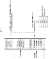
図13は実施形態に係る半導体装置の構成を示すブロック図である。
<Embodiment>
FIG. 13 is a block diagram illustrating a configuration of the semiconductor device according to the embodiment.
半導体装置(SD)は、同期クロックに従って、送信または受信の順序的な通信を行うインタフェース回路(SI)を備える。インタフェース回路(SI)は、送信状態および受信状態の少なくとも1つの状態である動作イネーブル状態を指定するレジスタ(REGISTER)と、動作イネーブル状態において、送信または受信の少なくとも1つのモードを変更するモード制御回路(MDC)と、を備える。
半導体装置によれば、送受信から送信または受信のモードの変更を容易にし、待機時間などを不要にして、通信のモードを変更可能にする。
The semiconductor device (SD) includes an interface circuit (SI) that performs sequential transmission or reception according to a synchronous clock. The interface circuit (SI) includes a register (REGISTER) that specifies an operation enable state that is at least one of a transmission state and a reception state, and a mode control circuit that changes at least one mode of transmission or reception in the operation enable state. (MDC).
According to the semiconductor device, it is possible to easily change the mode from transmission / reception to transmission / reception, to eliminate the standby time, and to change the communication mode.
図1Aは実施例に係るマイクロコンピュータの構成を示すブロック図である。マイクロコンピュータ(Micro Controller Unit:以下、MCUという。)10は1つの半導体基板上に図1Aに示す機能ブロックまたはモジュール等を備える半導体装置である。すなわち、MCU10は、中央処理装置(Central Processing Unit:以下、CPUという。)11、データ転送装置(データトランスファコントローラ(Data Transfer Controller:以下、DTCという。))12、割り込みコントローラ(Interrupt Controller:INT)13、リードオンリメモリ(Read Only Memory:以下、ROMという。)14およびランダムアクセスメモリ(Random Access Memory:以下、RAMという。)15を備える。MCU10は、さらに、バスコントローラ(Bus Controller:以下、BSCという。)16、タイマ(TIMER)17、SCI18、A/D(Analog/Digital)変換器およびD/A(Digital/Analog)変換器などのアナログモジュール(ANALOG)19および入出力ポート(I/O)1Aを備える。
FIG. 1A is a block diagram illustrating the configuration of the microcomputer according to the embodiment. A microcomputer (Micro Controller Unit: hereinafter referred to as MCU) 10 is a semiconductor device including the functional blocks or modules shown in FIG. 1A on one semiconductor substrate. That is, the
MCU10の動作の主体となるCPU11は、主にROM14から命令を読込んで動作する。ROM14は電気的に書換が可能なメモリであるフラッシュメモリ等の不揮発性メモリで構成される。DTC12は、CPU11の設定に基づき、CPU11に代ってデータ転送を行う。
The
INT13は、BSC16、タイマ17、SCI18、アナログモジュール19などからの割み込み要求(INTREQ)、およびMCU10外部からの複数の外部割り込み要求信号に基づく、I/O1Aからの割り込み要求(INTREQ)を受けて、CPU11に割り込み要求、またはDTC12にデータ転送起動要求を出力する。割り込み信号による処理を開始したときまたは終了したときに、割り込みをクリアする信号である割込みクリア信号(INTCLR)を、BSC16、タイマ17、SCI18、アナログ19、I/O1Aのそれぞれの割込み信号または割り込み要因フラグに対応して出力する。
The
BSC16は、CPU11およびDTC12からのバスリクエスト信号を受けてMCU内部バス1Bの占有に対する調停をして、バス使用許可信号を出力する。BSC16は、CPU11およびDTC12と、バスリクエスト、バスアクノレジ、バスコマンド、ウェイト、アドレス、データなどのインタフェースを行い、MCU内部バス1Bに接続された、RAM15やそのほかの機能ブロックまたはモジュールに対するリード/ライトを実現する。RAM15はSRAM等の揮発性メモリで構成される。
The
SCI18の送信データ出力(TXD)および受信データ入力(RXD)は、MCU10の外部のSCIとシリアルバスによって入出力される。このとき、必要に応じて入出力ポートを介して、入出力するようにすることもできる。
The transmission data output (TXD) and the reception data input (RXD) of the
図1Bは図1Aのマイクロコンピュータの主要なインタフェースを示すブロック図である。SCI18は、INT13を介して、DTC起動要求(DTCREQ)によりDTC12を起動する。SCI18のデータ転送起動要因として、コマンド受信完了(コマンド受信データフル)割り込み要求(CRXI)、データ受信完了(受信データフル)割り込み要求(DRX)、データ送信完了(送信データエンプティ)割り込み要求(TXI)を持つ。
FIG. 1B is a block diagram showing main interfaces of the microcomputer of FIG. 1A. The
DTC12は、INT13の示すDTCベクタ番号(DTCVEC)に対応した、データ転送情報をRAM15からリードして、データ転送を行う。データ転送情報は、データ転送起動要因に対応したものが用意される。後述のように、コマンド受信完了に対応したデータ転送によって、受信データフル(受信データ転送)、送信データエンプティ(送信データ転送)で使用するデータ転送情報を切り替えるようにする。また、DTC12はデータ転送時にアクノレジ信号(ACK)を活性化するとともに、データ転送情報または転送データに応じてモード制御信号(MDC)を出力する。このアクノレジ信号(ACK)とモード制御信号(MDC)は、INT13を介して、SCI18に与えられ、これに基づき、SCI18のモード制御部(SCIMDC)は後述するモードの変更を行う。SCI18は、モードと送受信の状態に従って、ステータス(ST)の出力を行う。
The
なお、データ転送装置の起動要因が一意に決まる場合には、SCI18とデータ転送装置を直接接続するようにしてもよい。これは、データ転送装置として、DTC12とINT13を一体化したものと理解することができる。
If the activation factor of the data transfer device is uniquely determined, the
(SCI)
図2は図1AのSCIの構成を示すブロック図である。SCI18は、制御レジスタ181、モード制御部(SCIMDC)182、送受信制御部(SCICNT)183、受信部184、送信部185、受信FIFO186、送信FIFO187等を備える。
(SCI)
FIG. 2 is a block diagram showing the configuration of the SCI in FIG. 1A. The
制御レジスタ181は、送受信の方式やフォーマットの指定を行うとともに、割り込み要求などの状態を表示するために、モードレジスタ(SMR)、コントロールレジスタ(SCR)、ステータスレジスタ(SSR)、ファンクションコントロールレジスタ(SFCR)を有する。例えば、SCRのトランスミットイネーブル(TE)ビット、レシーブイネーブル(RE)ビットのいずれかが1にセットされた状態に応じて、SCI18の動作イネーブル状態(SCIイネーブル)を指定する。この動作イネーブル状態は、ほかの送受信の方式やフォーマットの指定がなされた後に指定する。換言すれば、動作イネーブル状態では、送受信の方式やフォーマットの変更は行わない。
The
SCIMDC182は、制御レジスタ181のSFCRの設定に基づき、コマンド/データの識別(CMD)、送信抑止(TD)、受信抑止(RD)などのモード制御を行う。また、SCIMDC182は、DTC12のモード制御信号(MDC)に応じて、モードの切り替えを行う。このとき、SCIMDC182は、モード制御信号(MDC)をSCIMDC182内部で一旦、次モードとして保持し、実行中の送受信が完了した時点で、SFCRに反映するようにする。SCI18がスレーブ側である場合は、モードに対応してI/Oポート(端子18D)からステータス(ST)を出力する。コマンド受信が指定された状態での受信動作によって、ステータス(ST)出力をビジー状態にする。コマンド受信完了によるデータ転送装置の動作によって、モードの切り替えを行ったときに、ステータス(ST)出力をレディ状態にする。また、データ送信またはデータ受信動作によって、ステータス(ST)出力をビジー状態にし、これらによるデータ転送装置の動作によって、モードの切り替え(コマンド受信にモードを切り替え)たときに、レディ状態にする。
The
SCICNT183は、制御レジスタ181およびSCIMDC182に基づき、クロック部ボーレートジェネレータ(BRG)188からの同期クロック(SCK)に同期して、送信/受信/送受信動作を行う。また、SCI18がマスタ側である場合は、I/Oポート(端子18D)からステータス(ST)の入力を行い、ビジー状態の場合は、新たな送受信動作を開始しないようにする。
The
送信動作は、送信FIFO187に有効なデータが存在する状態で、同期クロック(SCK)が入力されると、送信部185を介して送信データ(TXD)を出力端子18Aに出力する。送信FIFO187に有効なデータがない状態で、同期クロック(SCK)が入力されると送信オーバランエラーを発生する。
In the transmission operation, when valid data exists in the
受信動作は、同期クロック(SCK)に同期して、入力端子18Bから受信データ(RXD)を受信部184に入力し、単位データの入力が行われると、受信FIFO186に転送する。受信FIFO186が一杯の状態で、さらに受信データを入力すると受信オーバランエラーを発生する。
In the reception operation, the reception data (RXD) is input from the
SCICNT183は、送信オーバランエラーまたは受信オーバランエラーが発生すると、INT13に割り込みを要求する。この割り込み処理ルーチンによって、CPU11は所要の処理を行い、SCI18は動作を再開することになる。
When a transmission overrun error or a reception overrun error occurs, the
SCICNT183は、送信FIFO187に所定の量の空きが生じた場合には送信データエンプティ割り込み要求(TXI)を、受信FIFO186に所定の量のデータが蓄積された場合は受信データフル割り込み要求(DRXI)を発生する。この所定の量は、制御レジスタ181の設定によって指定することができる。
The
制御レジスタ181において、TEビット、REビットがいずれも1にセットされた動作イネーブル状態においては、同期クロック(SCK)は送受信に共通であるため、送信動作と受信動作は同時に動作する。この動作イネーブル状態を送受信同時動作イネーブル状態という。送受信同時動作イネーブル状態であっても、送信オーバランエラーまたは受信オーバランエラーが発生した状態では、送受信動作は行わない。
In the operation enable state in which both the TE bit and the RE bit are set to 1 in the
SCICNT183は、送受信同時動作イネーブル状態においても、コマンド受信(CMD=1)の場合は、送信FIFO187に有効なデータがなくても、送信オーバランエラーを発生させず、送信動作を行い、また、送信FIFO187に有効なデータがあっても、送信FIFO187を保持したまま送信動作を行う。この送信動作では、送信出力を0または1に固定する。これは、TEビットを0に設定した場合と同様の動作である。また、SCICNT183は、単位データの受信によって、コマンド受信完了割り込み要求(CRXI)を発生させる。
Even when the simultaneous transmission / reception operation is enabled, the
送受信同時動作イネーブル状態においても、送信抑止(TD=1)の場合は、コマンド受信の場合と同様の動作になる。 Even in the transmission / reception simultaneous operation enabled state, when transmission is inhibited (TD = 1), the operation is the same as in the case of command reception.
SCICNT183は、送受信同時動作イネーブル状態においても、受信抑止(RD=1)の場合は、受信データは無視し、受信FIFO186も保持する。このため、受信データフル、受信オーバランエラーも発生させない。これは、REビットを0に設定した場合と同様の動作である。
Even in the transmission / reception simultaneous operation enabled state, the
受信部184は、入力端子18Bに接続され、1ビットずつ受信データ(RXD)を格納する。所定のデータ(例えば8ビット)の受信が完了すると、そのデータを受信FIFO186に転送する。後述のRDビットが1にセットされている場合は、受信完了とみなさない。受信FIFO186の内容は、MCU内部バス1Bを介して、CPU11またはDTC12からリードすることができる。
The receiving
送信FIFO187は、MCU内部バス1Bを介して、CPU11またはDTC12により、送信データのライトが行われる。後述のTDREフラグが0にクリアされ、送信が開始されると、送信FIFO187の内容は送信部185に転送される。送信部185は出力端子18Aに接続され、1ビットずつ送信データ(TXD)を出力する。
In the
ボーレートジェネレータ(BRG)188は、送受信の基本となるタイミングを生成することができるようにする。ボーレートジェネレータ(BRG)188は、ビットレートレジスタ、ビットレートカウンタを有する。 A baud rate generator (BRG) 188 makes it possible to generate timing that is the basis of transmission and reception. The baud rate generator (BRG) 188 has a bit rate register and a bit rate counter.
SCICNT183は、割り込み要求信号として、TXI(データ送信完了または送信データエンプティ割り込み要求)、CRXI(コマンド受信完了またはコマンド受信データフル割り込み要求)、DRXI(データ受信完了または受信データフル割り込み要求)、ERI(受信エラー割り込み要求)信号を出力する。TXI、CRXI、DRXI信号は、DTC12のデータ転送要求として使用することができる。
The
図3は図1AのSCIのレジスタ構成を示す図である。図3では、クロック同期式モードに関係するビットのみを示す。調歩同期式モードやそのほかの方式も、図示はされない、コントロールビット、ステータスフラグによって、実現することができる。 FIG. 3 is a diagram showing a register configuration of the SCI of FIG. 1A. FIG. 3 shows only the bits related to the clock synchronous mode. Asynchronous mode and other methods can also be realized by control bits and status flags not shown.
シリアルモードレジスタ(SMR)のビット1、0は、クロックセレクトビット(CKS1、CKS0)であり、内蔵ボーレートジェネレータ(BRG)188のクロックソースを選択する。
シリアルコントロールレジスタ(SCR)のビット7は、トランスミットインタラプトイネーブル(TIE)であり、TIEビットを1にセットすると、TXIが許可される。ビット6は、レシーブインタラプトイネーブル(RIE)であり、RIEビットを1にセットすると、RXIおよびERIが許可される。ビット5は、トランスミットイネーブル(TE)であり、TEビットを1にセットすると、送信動作が可能になる。ビット4は、レシーブイネーブル(RE)であり、REビットを1にセットすると、受信動作が可能になる。ビット1は、クロックイネーブル(CKE)であり、クロックソースおよびSCKの入出力端子18Cの機能を選択する。CKEビットが0にクリアされているときは、ボーレートジェネレータ(BRG)188からの内部クロックを使用し、入出力端子18CはSCKの出力端子となる。CKEビットが1にセットされているときは、外部クロックを使用し、入出力端子18CはSCKの入力端子となる。
MCU10が適用されるシステムによって、SCI18の動作は固定され、送信動作のみ(TE=1、RE=0)、受信動作のみ(TE=0、RE=1)、送受信同時動作(TE=RE=1)のいずれかになる。送受信コントロールは通信状態の遷移を司るにあたって、送信動作のみ、受信動作のみ、送受信同時動作の3つの動作によって、参照するレジスタやビットを変更する必要があり、送受信等の通信動作中に不整合を生じることを防ぐため、TE、REビットの通信動作中の切り替えは禁止される。TE、REビットを設定した後、ボーレートジェネレータ(BRG)188による基本クロックの同期化などの時間を待つ必要がある。
Depending on the system to which the
シリアルステータスレジスタ(SSR)のビット7は、トランスミットデータレジスタエンプティ(TDRE)フラグであり、送信FIFO187の空きの状態を表示する。所定の空きがある場合に、TDREフラグは1にセットされる。また、CPU11が、TDREフラグの1の状態をリードした後、0をライトしたとき、および、TXIにより起動されたDTC12で送信FIFO187へ送信データを転送したときに0にクリアされる。TDREフラグが0にクリアされると送信動作を開始する。ビット6は、レシーブデータレジスタフル(RDRF)フラグであり、受信FIFO186のデータの状態を表示する。受信FIFO186に所定のデータが存在する場合に、RDRFフラグは1にセットされる。また、CPU11が、RDRFフラグの1の状態をリードした後、0をライトしたとき、および、CRXIまたはDRXIにより起動されたDTC12で受信FIFO186からデータを転送したときに0にクリアされる。ビット5は、オーバランエラー(ORER)フラグであり、受信時にオーバランエラーが発生したことを表示する。具体的には、ORERフラグは、RDRFフラグが1にセットされた状態で次のデータを受信したときに、1にセットされる。このとき、受信データレジスタ(RDR)はオーバランエラーが発生する前の受信データを保持し、後から受信したデータが失われる。ORERフラグに1がセットされた状態では、以降のシリアル送受信は行わないようにする。
TDREフラグとTIEビットがいずれも1にセットされると、TXIが発生する。RDRFフラグとRIEビットが1にセットされると、後述のCMDビットによって、CRXIまたはDRXIが発生する。また、ORERフラグとRIEビットが1にセットされるとERIが発生する。 When both the TDRE flag and the TIE bit are set to 1, TXI occurs. When the RDRF flag and the RIE bit are set to 1, CRXI or DRXI is generated by a CMD bit described later. When the ORE flag and RIE bit are set to 1, ERI is generated.
ファンクションコントロールレジスタ(SFCR)のビット5は、送信ディスエーブル(TD)であり、クロック同期式モードの送受信動作時、かつクロック入力の状態で、TDビットが1にセットされている場合、TDREフラグの状態によらず、クロック入力に従って、送受信動作を開始する。送信データは固定値(例えば00またはFF)とする。0または1に固定することで、信号変化を抑止し、不所望の消費電力増加を回避することができる。データを固定するのみで、そのほかの通信動作は、送受信同時動作になる。ビット4は、受信ディスエーブル(RD)であり、RDビットを1にセットした場合は、受信を完了したとみなさず、RDRF、ORERフラグは1にセットされない。ビット2は、コマンド受信(CMD)であり、受信完了時にコマンド受信完了またはデータ受信完了のいずれとみなすかを指定する。すなわち、CMDビットが1にセットされている場合は、コマンド受信完了としてCRXIが発生し、CMDビットが0にクリアされている場合は、DRXIが発生する。
これらのCMD、TD、RDビットは、DTC12からのモード制御信号(MDC)に応じた、SCIMDC182に従い、変更される。
These CMD, TD, and RD bits are changed according to the
図4は図1AのSCIのモード制御状態遷移を示す図である。リセット後は、TE、REビットが0にされた停止状態ST1である。CPU11などにより、制御レジスタ181のSCRの設定を行い、TE、REビットの少なくとも1ビットを1にセットすると、動作イネーブル状態ST2になる。動作イネーブル状態ST2は、送信動作(TE=1)、受信動作(RE=1)または送受信動作(TE=RE=1)のいずれかの状態である。
FIG. 4 is a diagram showing mode control state transition of the SCI of FIG. 1A. After the reset, it is a stop state ST1 in which the TE and RE bits are set to 0. When the SCR of the
まず、特に制限はされないものの、DTC動作によるSFCR設定(モード制御)によってCMDビットを1にセットしてコマンド受信状態ST21にする。コマンド受信が完了すると、DTC12によるモード制御を待つ設定判定/待ち状態ST22になる。
First, although not particularly limited, the CMD bit is set to 1 by the SFCR setting (mode control) by the DTC operation to enter the command reception state ST21. When the command reception is completed, a setting determination / waiting state ST22 for waiting for mode control by the
このモード制御によってデータ受信状態ST23、データ送受信状態ST24、データ送信状態ST25のいずれかに遷移する。TDビットを1にセットするとデータ受信状態ST23に、RDビットを1にセットするとデータ送信状態ST25に、TDビットおよびRDビットのいずれも1にセットしない(0にクリアする)とデータ送受信状態ST24に遷移する。所要のデータ受信、データ送受信、データ送信を行うと、DTC12によるモード制御を待つ設定判定/待ち状態ST26になる。モード制御によってCMDビットを1にセットして、コマンド受信状態ST21に遷移する。なお、動作イネーブル状態ST2では、送受信の方式やフォーマットの変更は行わないようにする。
This mode control makes a transition to one of the data reception state ST23, the data transmission / reception state ST24, and the data transmission state ST25. When the TD bit is set to 1, the data reception state ST23 is set. When the RD bit is set to 1, the data transmission state ST25 is set. When neither the TD bit nor the RD bit is set to 1 (cleared to 0), the data transmission / reception state ST24 is set. Transition. When the required data reception, data transmission / reception, and data transmission are performed, the setting determination / waiting state ST26 for waiting for mode control by the
(INT)
図5は図1Aの割り込みコントローラ(INT)の構成を示すブロック図である。MCU10の割り込み要因には、内部割り込み、外部割り込みの2種類があり、それぞれ割り込み要因フラグを有する。ここでは、代表的にSCI18からの内部割り込み要因のみを示している。
(INT)
FIG. 5 is a block diagram showing a configuration of the interrupt controller (INT) of FIG. 1A. There are two types of interrupt factors of the
割り込みの要因フラグは、SCI18と同様に、タイマ17、アナログ19の機能ブロックが所定の状態になったときに、または、MCU10の外部割り込み入力端子が所定の状態になったときに、1にセットされる。割り込み要因フラグが1にセットされ、対応する割り込み許可ビットが1にセットされていると、INT13に割り込み要求される。
As with the
この割り込み要求(INTREQ)は、割り込み/DTC判定回路131に入力される。割り込み/DTC判定回路131には、さらにDTC許可レジスタ(DTER)132の内容が入力され、割り込み/DTC判定回路131は、割り込みが要求されたとき、DTC12を起動するか、CPU11に割り込みを許可するかを選択する。割り込み/DTC判定回路131は、DTC許可レジスタ132の当該割り込み要因に対応したDTEビットが1にセットされていると、DTC12への起動を要求し、CPU11への割り込みを要求しない。割り込み/DTC判定回路131は、DTC許可レジスタ132のDTEビットが0にクリアされていると、CPU11への割り込みを要求し、DTC12への起動を要求しない。
This interrupt request (INTREQ) is input to the interrupt /
割り込み/DTC判定回路131の出力は、CPU11への割り込み要求とDTC12への起動要求が独立にそれぞれ優先順位・マスクレベル判定回路133と優先順位判定回路134とに入力される。CPUの優先順位判定・マスクレベル判定回路133は、プライオリティレジスタ、割り込みマスクレベルなどに従って制御される。
The interrupt /
CPU11への割り込み要求、DTC12への起動要求のそれぞれについて、複数の割り込み要求が発生している場合に、優先順位・マスクレベル判定回路133および優先順位判定回路134はそれぞれ優先順位を判定する。この判定の結果、優先順位の最高のものが選択され、ベクタ番号が生成される。優先順位・マスクレベル判定回路133はCPU割り込み要求(CPUINT)とベクタ番号(VEC)を出力し、優先順位判定回路134はDTC起動要求(DTCREQ)とDTCベクタ番号(DTCVEC)を出力する。
When a plurality of interrupt requests are generated for each of the interrupt request to the
DTC起動要求(DTCREQ)はDTC12に入力され、またDTCベクタ番号(DTCVEC)はラッチ回路135に入力される。DTC動作開始信号(DTCSTA)およびDTC動作終了信号(DTCEND)がDTC12から出力され、ラッチ回路135に入力される。すなわち、DTC12が動作を開始すると、DTC動作開始信号(DTCSTA)が活性状態になり、ラッチ回路135はDTCベクタ番号(DTCVEC)のラッチおよび保持を行う。そして、DTC12のデータ転送が終了してDTC動作終了信号(DTCEND)が活性状態になり、ラッチ回路135のラッチは解除される。
The DTC activation request (DTCREQ) is input to the
また、DTCベクタ番号(DTCVEC)とDTC動作終了信号(DTCEND)はデコーダ回路136に入力され、対応する割り込み要因フラグ(例えばSCI18のTDRE,RDRF,ORER)に対してDTC12からの割り込み要因クリア信号(INTCLR)またはDTEクリア信号(DTECLR)が活性状態になって、割り込み要因フラグまたはDTEビットがクリアされる。
Also, the DTC vector number (DTCVEC) and the DTC operation end signal (DTCEND) are input to the
所要の割り込み要因で、DTC12を起動する場合、CPU11は予め、データ転送情報などをRAM15の所要のアドレスにライトするとともに、当該割り込みの割り込み許可ビット(例えばSCI18のTIE,RIE)と、DTC許可レジスタ132の当該割り込み要因に対応したDTEビットを1にセットしておく。
When the
この状態で当該割り込み要因フラグが1にセットされると、DTC12が起動される。DTC12が所定のデータ転送などの動作を実行している状態では、DTC12は割り込み要因クリア信号(INTCLR)によってデータ転送毎に当該割り込み要因フラグを0にクリアする。このとき、CPU11に割り込みは要求されない。
When the interrupt factor flag is set to 1 in this state, the
所定のデータ転送などを終了した場合、DTC12はDTEクリア信号(DTECLR)によって動作終了時にDTEビットを0にクリアする。このとき、当該割り込み要因フラグは1に保持され、DTEビットが0にクリアされているので、CPU11に割り込みが要求される。CPU11は、所定のデータ転送の終了などに対応した処理を実行するとともに、データ転送情報やDTEビットの再設定を行う。
When the predetermined data transfer or the like is finished, the
(DTC)
図6は図1AのDTCのデータ転送情報(転送情報セット)を示す図である。DTC12のデータ転送情報は、モードレジスタ(MR)、データレジスタ(DR)、第1および第2ソース(転送元)アドレスレジスタ(SAR1、SAR2)、デスティネーション(転送先)アドレスレジスタ(DAR)、転送カウントレジスタ(CR)からなる。
(DTC)
FIG. 6 is a diagram showing data transfer information (transfer information set) of the DTC of FIG. 1A. The data transfer information of the
MRに保持した内容によって、この内の必要なものが使用される。CRは、ブロック転送カウントレジスタ(BTCR)、転送カウントレジスタ(TCR)に分割され、TCRは8ビットずつ上位(TCRH)、下位(TCRL)に分割されている。後述のデータ転送モードに従って動作する。これらのレジスタ(MR、CR)は、1組分の回路がDTC12の内部に存在し、特に制限はされないものの、CPU11のアドレス空間上には存在しない。これらに格納されるべきデータ転送情報は、必要組数がCPU11のアドレス空間上の、RAM15などの所定のデータ転送情報アドレス領域に配置される。
Depending on the contents held in the MR, the necessary ones are used. The CR is divided into a block transfer count register (BTCR) and a transfer count register (TCR), and the TCR is divided into upper (TCRH) and lower (TCRL) by 8 bits. It operates according to a data transfer mode described later. These registers (MR, CR) have one set of circuits in the
モードレジスタ(MR)のビット構成は以下の通りである。
ビット31〜16は、データ転送モードの設定と、テーブル参照用の入力データの指定を行う。ビット15〜0は、テーブル参照用のデータ転送機能のテーブル参照の指定と、通常データ転送機能のデータ転送の指定を行う。
The bit configuration of the mode register (MR) is as follows.
ビット31は、TLUビットであり、通常データ転送またはテーブル参照用のデータ転送機能を選択する。TLUビットが0にクリアされた場合は、通常データ転送を行う。データ転送情報はMR、SAR2、DAR、CR(32ビット×4本)とされる。通常データ転送の説明において、ハードウェアとしてのSAR2を、データ転送情報としてはSARと記す。TLUビットが1にセットされた場合は、テーブル参照モードである。
ビット30は、BRMビットであり、TLUビットが1にセットされた場合に有効になり、分岐モードを指定する。データ転送情報はMR、SAR1、SAR2、DAR(32ビット×4本)とされる。CRは0とみなす。DTC12は、SAR1で指定したアドレスからリードしたデータに基づき、SAR2で指定したテーブルを参照する。DTC12は、テーブルからリードしたデータを、DARで指定した転送先アドレスにライトする。
ビット27は、MDCEビットである。DTC12は、MDCEビットが1にセットされた状態で、CR=0のデータ転送を行うと、モード制御信号(MDC)を出力する。
Bit 27 is the MDCE bit. The
ビット26〜24は、MDC[2:0]ビットである。TLUビットが0にクリアされ、MDCEビットが1にセットされた状態で、CR=0のデータ転送時に、モード制御信号(MDC)を指定する。MDC[2]ビットがCMDビットに、MDC[1]ビットがTDビットに、MDC[0]ビットがRDビットに反映されるようにする。DTC12は、TLUビットおよびMDCEビットがいずれも1にセットされた状態では、SAR2で指定したテーブルからリードしたデータに基づき、モード制御信号(MDC)を出力する。
Bits 26 to 24 are MDC [2: 0] bits. When the TLU bit is cleared to 0 and the MDCE bit is set to 1, a mode control signal (MDC) is designated at the time of data transfer with CR = 0. The MDC [2] bit is reflected in the CMD bit, the MDC [1] bit is reflected in the TD bit, and the MDC [0] bit is reflected in the RD bit. When both the TLU bit and the MDCE bit are set to 1, the
ビット22〜20は、SF[2:0]ビットであり、入力データの左シフトを8〜0ビットで指定する。 Bits 22 to 20 are SF [2: 0] bits, and specify a left shift of input data with 8 to 0 bits.
ビット17、16はISz[1:0]ビットであり、入力データのリードをバイトサイズ、ワードサイズ、ロングワードサイズのいずれで行うかを選択する。
ビット15、ビット14は、SM1、SM0ビットであり、データ転送後にSARをインクリメントするか、デクリメントするか、固定にするかを指定する。
ビット13、ビット12は、DM1、DM0ビットであり、データ転送後にDARをインクリメントするか、デクリメントするか、固定にするかを指定する。
ビット11、ビット10は、TMD1、TMD0ビットであり、データ転送モードを選択する。TMD1、TMD0ビットを00にするとノーマルモードとなる。このノーマルモードでは、1回の起動で、SARで示されるアドレスからDARで示されるアドレスへ1回のデータ転送を行う。この後、SM1、SM0、DM1、DM0ビットの指定に基づいてSAR、DARの操作が行われ、CRがデクリメントされる。これを起動要因が発生する毎に、CRで指定された回数だけ繰り返す。そして、CRで指定された回数のデータ転送が終了すると、DTC動作が禁止され、起動要因となった割り込みがCPU11に要求される。TMD1、TMD0ビットを01にするとリピートモードとなる。TMD1、TMD0ビットを10にするとブロック転送モードとなる。リピートモード、ブロック転送モードは、公知の技術で実現できる。
ビット9はDIRビットであり、転送元または転送先のいずれをリピート領域、ブロック領域とするかを選択する。 Bit 9 is a DIR bit, which selects whether the transfer source or the transfer destination is a repeat area or a block area.
ビット7、6はSz1、Sz0ビットであり、1回のデータ転送をバイトサイズ、ワードサイズ、ロングワードサイズのいずれで行うかを選択する。
ビット2はCREビットであり、CREビットを0にクリアした場合は、DTC起動要求(DTCREQ)に応じて、無制限にDTC12の動作を行う。ノーマルモードの場合はCRを使用しない。CREビットを1にセットした場合は、CRに初期設定した値に応じて、DTC12の動作を行う。
ビット1はNXTE1ビットであり、1つの起動要因に対してデータ転送を終了するか、次のデータ転送を行うかを選択する。このNXTE1ビットを0にクリアした場合、データ転送情報リードおよびデータ転送後、データ転送情報をライトしてDTCの動作を終了する。また、このNXTE1ビットを1にセットした場合、データ転送情報リードおよびデータ転送後、データ転送情報をライトして、さらに連続したアドレスからデータ転送情報をリードして、このデータ転送情報で指定されるデータ転送を行い、データ転送情報をライトする。これをチェイン転送と呼ぶ。ビット0はNXTE0ビットであり、CRが0になったときに、チェイン転送を行うかを指定する。
図7は図1AのDTCの構成を示すブロック図である。DTC12はデータ転送制御ブロック(DTCCNT)121、バスインタフェース(BIF)122、ベクタ生成ブロック(VG)123、ベクタアドレスレジスタ(VAR)124および演算器(ALU)12Aを備える。また、DTC12はモードレジスタ(MR)、第1ソースアドレスレジスタ(SAR1)、第2ソースアドレスレジスタ(SAR2)、デスティネーションアドレスレジスタ(DAR)およびデータ転送カウンタ(CR)を備える。
FIG. 7 is a block diagram showing the configuration of the DTC of FIG. 1A. The
DTCCNT121は、INT13からのDTC転送要求(DTCREQ)およびMRの内容に基づき、DTC12の制御を行う。
The
BIF122は、DTC内部バス12Bと、MCU内部バス1Bとのインタフェースを行う。このインタフェースには、バスリクエスト、バスアクノレジ、バスコマンド、ウェイト、アドレス、データなどを含む。また、BIF122は、データ転送制御ブロック(DTCCNT)121が転送データの確認を行うのにも使用される。
The
VG123は、INT13から与えられる割込みDTCベクタ番号(DTCVEC)に従って、ベクタアドレスを生成する。例えば、DTCVECを4倍などとし、所定のオフセットを加算する。
The
VAR124は、VG123で生成されたベクタアドレスが指し示すRAM15の領域からリードしたデータ転送情報の先頭アドレスを格納する。
The
MR、SAR1、SAR2、DAR、CRは、VAR124に格納されたデータ転送情報の先頭アドレスが指し示すRAM15の領域から順次リードしたデータ転送情報を格納する。
MR, SAR1, SAR2, DAR, and CR store data transfer information sequentially read from the area of the
ALU12Aは、論理演算、シフト、算術演算などの機能を持ち、所定の順序で、これらの演算の複数を実行にする。
The
DTC内部バス12Bは、図示はされないものの、複数のバスを持っており、SAR1、SAR2、DAR、CRの複数の内容を、ALU12Aに与えて演算できるようにする。これらによって、リピートモードやブロック転送モードの演算を行う。リピートモード、ブロック転送モードのデータ転送動作の内容については、公知の技術で実現できるので、詳細な説明は省略する。
Although not shown, the DTC internal bus 12B has a plurality of buses, and a plurality of contents of SAR1, SAR2, DAR, and CR are given to the
INT13からDTC起動要求信号(DTCREQ)が与えられると、DTC12は動作を開始する。DTCCNT121は、DTC12が動作を開始すると、DTC動作開始信号(DTCSTA)を活性状態にする。DTCCNT121は、データ転送を行うとき、このバスサイクルに応じて、アクノレジ信号(ACK)を活性化する。また、DTCCNT121は、転送カウンタ(CR)が0のとき、かつMRの設定に従い、モード制御信号(MDC)を所定の状態にし、SCI18のSFCRの設定を行う。DTCCNT121は、割り込み要因クリア信号(INTCLR)またはDTEクリア信号(DTECLR)を活性状態にし、起動要因となった割り込み要因フラグ又はDTEビットをクリアし、動作を終了する。DTCCNT121は、DTC12が動作を終了すると、DTC動作終了信号(DTCEND)を活性状態にし、停止状態に戻る。
When the DTC activation request signal (DTCREQ) is given from the
<応用例>
図8Aは応用例に係るマイクロコンピュータシステムの構成を示すブロック図である。図8Bは図8Aのマイクロコンピュータシステムの接続関係を示すブロック図である。マイクロコンピュータシステム1は、マスタMCU10M、スレーブMCU10S、モータ20、モータ20の位置を検出するエンコーダ30を含む。マイクロコンピュータシステム1は、例えばカメラシステムであり、カメラマスタMCU10Mはカメラボディ用MCUであり、スレーブMCU10Sはカメラレンズ用MCUである。
<Application example>
FIG. 8A is a block diagram showing a configuration of a microcomputer system according to an application example. FIG. 8B is a block diagram showing the connection relationship of the microcomputer system of FIG. 8A. The
実施例に係るMCU10は、マスタMCU10MおよびスレーブMCU10Sに適用される。スレーブMCU10Sは、焦点モータ(M)20の駆動用のタイマ17F、焦点モータ20の位置を検出するためのエンコーダ(ENCODER)の入力用のタイマ17D、インターバルタイマ機能を持つタイマ17Iを使用するものとする。また、各種設定のスイッチ(SWITCH)などを、入出力ポート(I/O)1Aで入力する。
The
図8Bに示すように、マスタMCU10MのSCI18、スレーブMCU10SのSCI18はクロック同期式モードの3本およびステータスを示す入出力ポートの1本の信号線でインタフェースを行う。マスタMCU10MのTXDを出力する端子18A、RXDを入力する端子18B、SCKを出力する端子18CおよびSTを入力する端子18Dのそれぞれが、スレーブMCU10SのRXDを入力する端子18B、TXDを出力する端子18A、SCKを入力する端子18CおよびSTを出力する端子18Dに接続される。マスタMCU10Mが同期クロック(SCK)を出力し、スレーブMCU10Sがステータス(ST)を出力する。
As shown in FIG. 8B, the
(通信動作の第1の例)
図9は図8Aのマイクロコンピュータシステムにおける通信動作の第1の例を示すタイミング図である。通信動作の第1の例はマスタ送信/スレーブ受信の場合である。図9において、網掛け部が、スレーブMCU10SのSCI18のモード制御を行う、DTC12の動作を示す。
(First example of communication operation)
FIG. 9 is a timing chart showing a first example of communication operation in the microcomputer system of FIG. 8A. A first example of the communication operation is a case of master transmission / slave reception. FIG. 9 shows the operation of the
まず、マスタMCU10MおよびスレーブMCU10SはそれぞれのSCI18のレジスタに送受信動作(TE=1、RE=1)として初期設定を行う(タイミングT1)。
First, the
マスタMCU10Mは、スレーブMCU10Sのステータス(ST)出力を入力して、これがビジー(BUSY)状態である場合は、送信を待機する。送信データ(コマンド)が設定され、ステータス(ST)入力がレディ(READY)状態になると、マスタMCU10Mは、コマンド(CMND)を送信する。このとき、マスタMCU10MはRDビットを1にセットし、受信データを無視するようにする。
The
スレーブMCU10Sは、CMDビットを1にセットし、TDビットを1にセットしてコマンド受信に設定する(タイミングT1)。送信データエンプティ割り込み要求(TXI)のセットは抑止され、送信FIFO187へのデータ設定を行わず、送信データ(TXD)は、例えばハイレベルに固定され、ダミー(DUMY)データが出力される。受信が開始されると、ステータス(ST)出力をビジー状態にする。SCI18は、コマンドの受信が完了されると、コマンド受信完了割り込み要求(CRXI)を発生し、INT13はDTC12にDTC起動要求(DTCREQ)を発生する。DTC12は、コマンドの受信データをリードして、これをSAR2に加算して、RAM15のテーブル領域をリードする。この内容は、DARで指定される送信データエンプティ(送信データ転送)、受信データフル(受信データ転送)によるデータ転送起動要求のDTCベクタ(TXIベクタ、DRXIベクタ)を設定する。本例では、ロングワード2個をブロック転送するものとする。2個のロングワードの一方が所定のデータの場合(例えば、00000000の場合)、対応するTDビットまたはRDビットを1にセットするように、モード制御信号(MDC)を活性化する。具体的には、送信データエンプティのDTCベクタが00000000の場合、TDビットを1にセットし、送信抑止とする。受信データフルのDTCベクタが00000000の場合、RDビットを1にセットし、受信抑止とする。CMDビットは0にクリアする。このモード制御信号(MDC)に従い、SCI18はSFCRの設定を行って、データ受信またはデータ送信に切り替えるとともに、ステータス(ST)出力をビジー状態にする。この場合、先のコマンドに応じて、マスタの送信/スレーブの受信、スレーブの送信/マスタの受信、マスタ/スレーブの送受信の3つの態様がある。本例では、マスタの送信/スレーブの受信を行う場合であるので、マスタはRDビットを1にセットして受信抑止(データ送信)に設定し、スレーブはTDビットを1にセットして送信抑止(データ受信)に設定する(タイミングT2)。
The
マスタMCU10Mはコマンド送信完了後、送信データが設定され、ステータス(ST)入力がレディ状態になると、コマンドに対応した、所定の数のデータを送信する。
The
スレーブMCU10Sは、データ受信の開始時に、ステータス(ST)出力をビジー状態にする。データの受信が完了に従い、受信データフル(受信データ転送)データ転送起動要求を行い、DTC12を起動する。DTC12は受信したデータをRAM15の所定のアドレスに転送する。CRにはコマンドに対応した、所定の数のデータを設定しておき、これに従った個数のデータ転送を行い、CRが0になると、MRで指定したモード制御信号(MDC)を出力し、SCI18のモード制御状態を遷移させる(タイミングT3)。SCI18はこれによって、ステータス(ST)出力をレディ状態にする。CRが0のデータ転送が完了すると、CPU11に割り込みを要求する。
The
図10は図9の第1の例におけるコマンド受信完了のためのデータ転送を示す図である。スレーブMCU10Sのコマンド受信完了のためのデータ転送においては、データ転送情報を以下のようにCPU11が設定する。
FIG. 10 is a diagram showing data transfer for command reception completion in the first example of FIG. In the data transfer for completing the command reception of the
MRのTLUビット、BRMビット、MDCEビットをいずれも1にセットする。SF[2:0]ビットは+4を指定する。ISz[1:0]ビットは、コマンドに対応したバイトサイズを指定する。SM1、SM0ビットは、SAR2固定を指定する。DM1、DM0ビットは、DAR固定を指定する。TMD1、TMD0ビットはノーマルモードを指定する。SAR1は受信FIFO186のアドレスを、SAR2は、データ送信エンプティ転送要求、データ受信フル転送要求のDTCベクタのテーブル領域の先頭アドレスを指定する。DARは、データ送信エンプティ転送要求、データ受信フル転送要求のDTCベクタアドレスを指定する。これらは図10のデータ転送情報Cとして格納される。
The TLU bit, BRM bit, and MDCE bit of MR are all set to 1. The SF [2: 0] bits specify +4. The ISz [1: 0] bits specify the byte size corresponding to the command. The SM1 and SM0 bits specify SAR2 fixed. The DM1 and DM0 bits specify DAR fixed. The TMD1 and TMD0 bits specify the normal mode. SAR1 designates the address of the
図10において、細線の矢印はアドレスの指定を、二重線の矢印はデータのリード/ライトを示す。
(A)コマンド受信完了によって、DTCが起動されると、対応するベクタ領域(CRXI割込みのベクタアドレスが指定する領域(CRXIベクタ))から、データ転送情報の先頭アドレスをリードする。
(B)このアドレスに基づいて、データ転送情報アドレス領域からデータ転送情報Cをリードする。このデータ転送情報Cは、MR、SAR1、SAR2、DARに格納すべき内容である。SAR1には受信FIFO186のアドレスが、SAR2にはテーブル領域の先頭アドレスが、DARにはTXIベクタアドレスが格納される。
(C)まず、SAR1で指定した受信FIFO186から、ISzビットで指定したバイトサイズの、コマンドをリードする。リードしたデータは、ALU12Aで、SF[2:0]ビットで指定した4ビットの左シフトし、この結果を、SAR2に加算して転送元アドレスとして使用する。
(D)SAR2で指定した、テーブル領域の転送元アドレスから転送データをリードする。本例では、TXIベクタn、DRXIベクタnをリードする。
(E)これをDARで示す、TXIベクタおよびDRXIベクタ領域へのライトを行う。同時に、前記の通り、モード制御信号(MDC)を出力する。
例えば、DRXIベクタnは所要のデータ転送情報mなどを示す内容とする。
In FIG. 10, thin line arrows indicate address designation, and double line arrows indicate data read / write.
(A) When DTC is activated upon completion of command reception, the head address of the data transfer information is read from the corresponding vector area (area specified by the vector address of the CRXI interrupt (CRXI vector)).
(B) Based on this address, the data transfer information C is read from the data transfer information address area. This data transfer information C is content to be stored in MR, SAR1, SAR2, and DAR. The address of the
(C) First, a command having a byte size designated by the ISz bit is read from the
(D) Read the transfer data from the transfer source address of the table area specified by SAR2. In this example, the TXI vector n and the DRXI vector n are read.
(E) Write to the TXI vector and DRXI vector areas indicated by DAR. At the same time, the mode control signal (MDC) is output as described above.
For example, the DRXI vector n has contents indicating required data transfer information m and the like.
これによって、コマンドに対応した、TXIおよびDRXIデータ転送に応じた、データ転送情報を(データ転送情報m、m1、m2、m3などから)選択可能にできる。 This makes it possible to select data transfer information (from data transfer information m, m1, m2, m3, etc.) corresponding to the command and corresponding to TXI and DRXI data transfer.
なお、コマンドはバイトサイズの場合、最大256通りを指定することができる。後続するデータの有無やデータ長、データの種類などを定義する。例えば、後続するデータを、スレーブMCU10Sのタイマ17D,17F,17IやI/Oポート1Aへライトすることを指示したり、スレーブMCU10Sのタイマ17D,17F,17IやI/Oポート1Aの所望のデータを送信することを指示したりする。かかるコマンドは、当該マイクロコンピュータシステム1に適切なものを、任意に定義することができる。
In the case of a byte size, up to 256 commands can be specified. Defines the presence / absence of data, data length, data type, etc. For example, it is instructed to write subsequent data to the
図11は図9の第1の例における受信データフル(受信データ転送)のためのデータ転送を示す図である。スレーブMCU10Sの受信データフル(受信データ転送)のためのデータ転送においては、データ転送情報を以下のように設定する。
FIG. 11 is a diagram showing data transfer for reception data full (reception data transfer) in the first example of FIG. In the data transfer for the reception data full (reception data transfer) of the
MRのTLUビット、BRMビットを0にクリアし、MDCEビットを1にセットする。Sz[1:0]ビットは、コマンドに対応したバイトサイズを指定する。SM1、SM0ビットは、SAR固定を指定する。DM1、DM0ビットは、DARインクリメントを指定する。TMD1、TMD0ビットはノーマルモードを指定する。SARは受信FIFO186のアドレスを、DARはデータ受信用のRAM15のアドレスを、CRはコマンドに対応したデータ数を指定する。これらは図11のデータ転送情報mとして格納される。
(A)受信データフル(受信データ転送)によって、DTC12が起動されると、対応するベクタ領域(DRXI割込みのベクタアドレスが指定する領域(DRXIベクタ))から、データ転送情報先頭アドレスをリードする。これはコマンド受信完了によるデータ転送によって、所要の内容に更新され、データ転送情報mを示すようにされている。
(B)このアドレスに基づいて、データ転送情報アドレス領域からデータ転送情報mをリードする。このデータ転送情報は、MR、SAR、DAR、CRの内容である。SARには受信FIFO186のアドレスが、DARにはRAM15のアドレスが格納される。
(C)まず、SARで指定した受信FIFO186から、Szビットで指定したバイトサイズの、受信データをリードする。リードした受信データは、DARで指定したRAM15などにライトする。これをCRで指定した回数繰り返し、CR=0となると、前記の通り、モード制御信号(MDC)を出力する。
Clear the MR TLU and BRM bits to 0 and set the MDCE bit to 1. The Sz [1: 0] bits specify the byte size corresponding to the command. The SM1 and SM0 bits specify SAR fixed. The DM1 and DM0 bits specify DAR increment. The TMD1 and TMD0 bits specify the normal mode. SAR designates the address of the
(A) When the
(B) Based on this address, the data transfer information m is read from the data transfer information address area. This data transfer information is the contents of MR, SAR, DAR, and CR. The address of the
(C) First, the reception data of the byte size specified by the Sz bit is read from the
(通信動作の第2の例)
図12は図8Aのマイクロコンピュータシステムにおける通信動作の第2の例を示すタイミング図である。通信動作の第2の例では、コマンドに対応したデータ転送が、スレーブの送信/マスタの受信の場合である。マスタMCU10MおよびスレーブMCU10Sはそれぞれ送受信動作として初期設定を行うこと、コマンドの送信/受信は、上述の第1の例と同様である。
(Second example of communication operation)
FIG. 12 is a timing chart showing a second example of communication operation in the microcomputer system of FIG. 8A. In the second example of the communication operation, the data transfer corresponding to the command is a case of slave transmission / master reception. Each of the
マスタMCU10Mは、所要のデータの数に相当する同期クロックを出力するため、TDビットを1にセットして、例えば送信データをハイレベルに固定してダミーのデータを送信する。
In order to output a synchronous clock corresponding to the number of required data, the
スレーブMCU10Sは、コマンド受信完了時のDTC12のモード制御によって、RDビットを1にセットしてデータ送信に設定するようにする(タイミングT2)。すなわち、RAM15のテーブル上の送信データエンプティのDTCベクタを00000000以外の所定のベクタにし、受信データフルのDTCベクタを00000000にする。
The
スレーブMCU10Sは、コマンドに対応した、所定の数のデータを送信するため、送信データエンプティ(送信データ転送)データ転送要求に従い、DTC12Sを起動する。DTC12は、送信すべきデータをRAM15の所定のアドレスから送信FIFO187に転送する。データ送信の開始時に、ステータス(ST)出力をビジー状態にする。CRで示される、予め決められた個数のデータ転送を行い、CRが0になると、MRで指定したモード制御信号(MDC)を出力し、SCI18Sのモード制御状態を遷移させる(タイミングT3’)。このとき、モードの変更、またはSFCRの変更は直ちに反映されず、送信データの出力完了後に(送信FIFO187および送信部185にデータがなくなった状態で)反映する(タイミングT3)。言い換えると、モード制御入力を送受信に同期させて反映させる。SCI18Sはステータス(ST)出力をレディ状態にする。CRが0のデータ転送が完了すると、SCI18SはCPU11に割り込みを要求する。
The
送信データエンプティ(送信データ転送)のためのデータ転送においては、データ転送情報を以下のように設定する。 In data transfer for transmission data empty (transmission data transfer), data transfer information is set as follows.
MRのTLUビット、BRMビットを0にクリアし、MDCEビットを1にセットする。Sz[1:0]ビットは、コマンドに対応したバイトサイズを指定する。SM1、SM0ビットは、SARインクリメントを指定する。DM1、DM0ビットは、DAR固定を指定する。TMD1、TMD0ビットはノーマルモードを指定する。SARはデータ送信用のRAM15Sのアドレスを、DARは送信FIFO187のアドレスを、CRはコマンドに対応したデータ数を指定する。
Clear the MR TLU and BRM bits to 0 and set the MDCE bit to 1. The Sz [1: 0] bits specify the byte size corresponding to the command. The SM1 and SM0 bits specify SAR increment. The DM1 and DM0 bits specify DAR fixed. The TMD1 and TMD0 bits specify the normal mode. SAR designates the address of the RAM 15S for data transmission, DAR designates the address of the
(通信動作の第3の例)
通信動作の第3の例であるマスタ/スレーブの送受信の場合は、図示を省略するが、スレーブMCU10Sは、TDビット、RDビットをいずれも0にクリアし、DTC12が送信データ完了によるデータ転送時にはSFCRの変更の制御を行わず、受信データ完了によるデータ転送時にはSFCRの変更の制御を行うようにする。すなわち、RAM15のテーブル上の送信データエンプティ、受信データフルのDTCベクタを、いずれも00000000以外の所定のベクタにする。
(Third example of communication operation)
In the case of master / slave transmission / reception, which is a third example of communication operation, although not shown, the
以上の実施例によれば以下の作用効果を得るものである。
(1)送信および受信がイネーブルとされた状態(TE=RE=1)において(送受信同時動作を指定したまま)、TDビットまたはRDビットを1に設定することにより、送信または受信の一方の動作を抑止可能にする。送信動作抑止の場合は、送信データの用意や送信開始の指定を必要とせず、同期クロック入力に対応して、任意データの送信と、受信動作を可能にする。受信動作抑止の場合は、受信した内容を無視しオーバランエラーも検出しないようにし、割り込み要求やデータ転送起動要求を行わないようにする。これにより、送受信同時動作かつ同期クロック入力での動作イネーブル状態において、一時的に、換言すれば、設定変更の待機時間などを不要としながら、送信動作抑止、受信動作抑止が可能になる。無駄な送信データの準備や、無駄な受信データの処理などを不要とし、処理を効率化できる。TEビットまたはREビットを切り替えると、SCI全体の動作との整合を図る必要があるのに対し、送受信同時動作の基本的な動作は変更せず、TDビットおよびRDビットの制御対象を限定することで、論理を簡略化することができる。不所望の状態に陥る可能性を低減することができる。
(2)受信動作において、コマンドを受信する動作であるか、データを受信する動作であるかを指定可能にし、これらの割り込み要求またはデータ転送起動要求を別々に要求するようにする。これによって、データ転送装置の起動要因を専用にすることが可能になる。コマンド受信する動作時は、送信動作抑止とすることにより、送信データの用意を不要にする。データ受信する動作時では、送信動作の抑止を指定可能にする。コマンド受信完了の割り込み要求、データ受信完了の割り込み要求を分離することにより、いずれかの判断を行うことなく、必要な処理を直ちに実行することができる。コマンド受信完了の割り込み要求に対してはデータ転送装置によるデータ転送を行い、データ受信完了の割り込み要求に対してはCPUによる割り込み処理を行うなどの、好適な処理方法の選択を効率的にすることができる。
According to the above embodiment, the following operational effects are obtained.
(1) In a state where transmission and reception are enabled (TE = RE = 1) (while specifying the simultaneous transmission / reception operation), by setting the TD bit or the RD bit to 1, one operation of transmission or reception Can be suppressed. In the case of the transmission operation inhibition, it is not necessary to prepare transmission data or specify transmission start, and enables transmission and reception of arbitrary data corresponding to the synchronous clock input. When the reception operation is suppressed, the received content is ignored so that no overrun error is detected, and no interrupt request or data transfer start request is issued. This makes it possible to suppress the transmission operation and the reception operation while temporarily eliminating the need for a setting change waiting time, for example, in an operation enable state with simultaneous transmission and reception and synchronous clock input. Preparation of useless transmission data, processing of useless reception data, and the like are unnecessary, and the processing can be made efficient. When switching the TE bit or RE bit, it is necessary to match the operation of the entire SCI, but the basic operation of the simultaneous transmission / reception operation is not changed, and the control target of the TD bit and the RD bit is limited. Thus, the logic can be simplified. The possibility of falling into an undesired state can be reduced.
(2) In the receiving operation, it is possible to specify whether the operation is to receive a command or to receive data, and to request these interrupt requests or data transfer activation requests separately. This makes it possible to dedicate the activation factor of the data transfer device. When the command is received, the transmission data is not required to be prepared by suppressing the transmission operation. It is possible to specify the suppression of the transmission operation when receiving data. By separating the interrupt request for command reception completion and the interrupt request for data reception completion, it is possible to immediately execute necessary processing without making any determination. Efficient selection of a suitable processing method, such as performing data transfer by the data transfer device in response to an interrupt request for completion of command reception, and performing interrupt processing by the CPU in response to an interrupt request for completion of data reception Can do.
(3)コマンド受信、データ受信のみ、データ送信のみ等のモードおよび起動要因に応じたデータ転送装置の動作によって、モードを切り替える。例えば、データ送信またはデータ受信に対応した、データ転送装置によるデータ転送の完了時に、コマンド受信に切り替える。
(4)モードに対応したステータスを出力可能にする。コマンド受信が指定された状態での受信動作によって、外部へのステータス出力を第2状態(ビジー)にする。コマンド受信完了によるデータ転送装置の動作によって、モードの切り替えを行ったときに、外部へのステータス出力を第1状態(レディ)にする。また、データ送信またはデータ受信動作によって、ステータス出力を第2状態(ビジー)にし、これらによるデータ転送装置の動作によって、モードの切り替え(コマンド受信にモードを切り替え)たときに、第1状態(レディ)にする。
これらによって、実際の通信処理に応じたモードを実現可能にするとともに、設定変更や待機時間を減らすことができる。モードと通信動作に応じて、データ転送装置を起動し、データ転送装置の制御によって、モードを切り替えるようにして、CPUの処理を不要にし、効率化と高速化を実現することができる。データ転送装置がCPUに代わって、SCIのモード制御や、コマンドの判定、データ転送を実行可能にすることで、CPUに割り込みを要求する頻度を低減したり、CPUを低消費電力状態にする期間を長くしたりすることができる。CPUが割り込み処理にあたって実行すべき、例外処理、スタックの退避・復帰操作、復帰命令の実行を不要とすることができ、プログラムの簡略化やシステムの効率化に寄与することができる。また、イベントの発生から所要の動作の実行までの時間を短縮し、いわゆる応答性を向上することができる。CPUより論理規模が小さく、かつ高速に処理を行うことができるデータ転送装置が動作し、CPUを低消費電力状態にすることで、低消費電力化を実現することができる。また、ソフトウェアの開発効率を向上することができる。
(3) The mode is switched according to the mode of command reception, data reception only, data transmission only, and the like and the operation of the data transfer device according to the activation factor. For example, when data transfer by the data transfer device corresponding to data transmission or data reception is completed, switching to command reception is performed.
(4) The status corresponding to the mode can be output. The status output to the outside is set to the second state (busy) by the reception operation in the state where command reception is designated. When the mode is switched by the operation of the data transfer apparatus upon completion of command reception, the status output to the outside is set to the first state (ready). Also, the status output is set to the second state (busy) by the data transmission or data reception operation, and when the mode is switched (the mode is switched to command reception) by the operation of the data transfer device by these, the first state (ready) is set. ).
As a result, a mode according to actual communication processing can be realized, and setting change and standby time can be reduced. Depending on the mode and the communication operation, the data transfer device is activated, and the mode is switched under the control of the data transfer device, so that the processing of the CPU is unnecessary, and the efficiency and speed can be realized. A period in which the data transfer apparatus can execute SCI mode control, command determination, and data transfer on behalf of the CPU, thereby reducing the frequency of requesting an interrupt to the CPU or putting the CPU in a low power consumption state. Can be lengthened. Exception processing, stack save / restore operations, and execution of return instructions that should be executed by the CPU for interrupt processing can be eliminated, which contributes to simplification of the program and efficiency of the system. In addition, the time from the occurrence of an event to the execution of a required operation can be shortened, and so-called responsiveness can be improved. A data transfer apparatus that is smaller in logical scale than the CPU and capable of performing processing at high speed operates, and the CPU is brought into a low power consumption state, whereby low power consumption can be realized. In addition, software development efficiency can be improved.
マイクロコンピュータシステムのそれぞれに適切なコマンドや通信方式に、柔軟に対応することができる。換言すれば、マイクロコンピュータへ与えるデータによって、マイクロコンピュータの送受信の態様を変更可能にすることができる。 It is possible to flexibly cope with commands and communication methods suitable for each microcomputer system. In other words, the transmission / reception mode of the microcomputer can be changed by the data given to the microcomputer.
以上、本発明者らによってなされた発明を実施形態、実施例および応用例に基づき具体的に説明したが、本発明は、実施形態、実施例および応用例に限定されるものではなく、種々変更可能であることはいうまでもない。 As mentioned above, the invention made by the present inventors has been specifically described based on the embodiments, examples and application examples. However, the present invention is not limited to the embodiments, examples and application examples, and various modifications are made. It goes without saying that it is possible.
本実施例では、SCIの設定完了後の動作の許可として、TEビット、REビットを使用する仕様とし、これとは独立のTDビット、RDビットを設けたが、SCIの動作イネーブルビットを、送信および受信に共通に設け、TEビットおよびREビットと、TDビットおよびRDビットとの機能を併せるようにし、動作中に変更可能にしてもよい。コマンド受信および送信抑止の場合の送信出力は任意であってよいが、0または1に固定することが好ましい。CMDビットを1にセットした場合は、TDビットに関わらず、送信抑止としてもよい。CRXI、DRXIの割り込み要因フラグは共通のRDRFフラグとせずに、独立の割り込み要因フラグとしてもよい。RDビットを1にセットしたときに、RIEビットまたはRDRFフラグを0にクリアするようにしてもよい。TDビット、RDビットを指定するためのロングワードデータは、データ転送情報格納領域として使用しないデータとすればよい。本実施例では00000000としたが、これはCPUのリセットベクタと共通であり、データ転送情報格納領域として使用しないことを想定したものである。データ転送格納アドレスはロングワード単位と考える場合、下位の2ビットを使用してもよい。 In the present embodiment, the TE bit and the RE bit are used to permit the operation after the completion of the SCI setting. The TD bit and the RD bit are provided independently of this, but the SCI operation enable bit is transmitted. It may be provided in common for reception, and the functions of the TE bit and RE bit, and the TD bit and RD bit may be combined to be changed during operation. The transmission output in the case of command reception and transmission suppression may be arbitrary, but is preferably fixed to 0 or 1. When the CMD bit is set to 1, transmission may be suppressed regardless of the TD bit. The CRXI and DRXI interrupt factor flags may be independent interrupt factor flags instead of the common RDRF flag. When the RD bit is set to 1, the RIE bit or the RDRF flag may be cleared to 0. The long word data for designating the TD bit and the RD bit may be data that is not used as the data transfer information storage area. In this embodiment, 00000000 is assumed, but this is common with the reset vector of the CPU and is assumed not to be used as a data transfer information storage area. When considering the data transfer storage address as a long word unit, the lower 2 bits may be used.
受信FIFO、送信FIFOが受信データフル(受信データ転送)、送信データエンプティ(送信データ転送)を検出するための、空きやデータ量を、制御レジスタによって変更可能にしてもよい。また、コマンド受信のときの受信完了を判定する単位も、バイトサイズ以外に選択可能にしてもよい。コマンド受信完了によるデータ転送によって、ベクタ領域を書き換えるほか、データ転送情報を書き換えるようにしてもよい。CPUによって、CMDビット、TDビット、RDビットを設定可能にしてもよい。任意のコマンドをCPUが処理するようにし、CMDビット、TDビット、RDビットを設定するようにしてもよい。 The reception register and the transmission FIFO may be able to change the vacancy and the data amount for detecting reception data full (reception data transfer) and transmission data empty (transmission data transfer) by a control register. The unit for determining the completion of reception at the time of command reception may be selectable in addition to the byte size. In addition to rewriting the vector area by data transfer upon completion of command reception, the data transfer information may be rewritten. The CPU may be able to set the CMD bit, TD bit, and RD bit. Arbitrary commands may be processed by the CPU, and the CMD bit, TD bit, and RD bit may be set.
本実施例ではSCIを例に説明したが、これに限定されるものではなく、I2C(Inter-Integrated Circuit)、SPI(Serial Peripheral Interface)等のシリアル通信インタフェースに適用することができる。本実施例ではDTCを例に説明したが、これに限定されるものではなく、DMAC(Direct Memory Access Controller)等のメモリとレジスタ等の間でデータを転送するものであってもよい。DTC、割り込みコントローラの具体的な構成についても種々変更可能である。BSCや、バス権やウェイトなどのバス動作の詳細については省略したが、これらは適宜実装可能である。マスタMCU、スレーブMCUの一方のみに適用してもよい。この場合、スレーブMCUに適用するのが好ましい。 In this embodiment, the SCI has been described as an example. However, the present invention is not limited to this, and can be applied to a serial communication interface such as an I 2 C (Inter-Integrated Circuit) or SPI (Serial Peripheral Interface). In this embodiment, the DTC has been described as an example. However, the present invention is not limited to this, and data may be transferred between a memory such as a DMAC (Direct Memory Access Controller) and a register. Various modifications can be made to the specific configurations of the DTC and the interrupt controller. Details of bus operations such as BSC and bus rights and waits have been omitted, but these can be implemented as appropriate. You may apply only to one of a master MCU and a slave MCU. In this case, it is preferable to apply to the slave MCU.
マイクロコンピュータの構成についても限定されない。そのほかや機能ブロックなども種々変更できる。以上の説明ではマイクロコンピュータに適用した場合について説明したが、それに限定されるものではなく、その他の半導体装置、例えば、デジタルシグナルプロセッサ(DSP)に適用することができる。 The configuration of the microcomputer is not limited. In addition, various functional blocks can be changed. In the above description, the case where the present invention is applied to a microcomputer has been described. However, the present invention is not limited thereto, and can be applied to other semiconductor devices such as a digital signal processor (DSP).
<実施態様>
以下、実施態様について付記する。
(付記1)
同期クロックに従って送信または受信の順序的な通信を行うインタフェース回路を有する半導体装置であって、
前記インタフェース回路は、
送信状態及び受信状態の少なくとも一つの状態である動作イネーブル状態を指定する第1のレジスタと、
送信抑止または受信抑止を指定することが可能な情報を有する第2のレジスタと、
を有し
前記第1のレジスタと前記第2のレジスタの状態に基づいて情報の送信または受信の少なくとも一つの動作を決定する
半導体装置。
<Embodiment>
Hereinafter, the embodiment will be additionally described.
(Appendix 1)
A semiconductor device having an interface circuit that performs sequential communication of transmission or reception according to a synchronous clock,
The interface circuit is
A first register that specifies an operation enable state that is at least one of a transmission state and a reception state;
A second register having information capable of specifying transmission suppression or reception suppression;
A semiconductor device that determines at least one operation of transmitting or receiving information based on states of the first register and the second register.
(付記2)
同期クロックに従って、送信または受信の順序的な通信を行う第1のインタフェース回路を備える第1の半導体装置と、
前記同期クロックに従って、送信または受信の順序的な通信を行う第2のインタフェース回路を備える第2の半導体装置と、
を備えるシステムであって、
前記第2のインタフェース回路は、
送信状態及び受信状態の少なくとも一つの状態である動作イネーブル状態を指定する第1のレジスタと、
送信抑止または受信抑止を指定することが可能な情報を有する第2のレジスタと、
を有し
前記第1のレジスタと前記第2のレジスタの状態に基づいて情報の送信または受信の少なくとも一つの動作を決定する
システム。
(Appendix 2)
A first semiconductor device including a first interface circuit that performs sequential transmission or reception in accordance with a synchronous clock;
A second semiconductor device comprising a second interface circuit for performing sequential transmission or reception in accordance with the synchronous clock;
A system comprising:
The second interface circuit includes:
A first register that specifies an operation enable state that is at least one of a transmission state and a reception state;
A second register having information capable of specifying transmission suppression or reception suppression;
And determining at least one operation of transmitting or receiving information based on states of the first register and the second register.
1・・・マイクロコンピュータシステム
10・・・マイクロコンピュータ
11・・・中央処理装置(CPU)
12・・・データトランスファコントローラ(DTC)
121・・・データ転送制御ブロック(DTCCNT)
122・・・バスインタフェース(BIF)
123・・・ベクタ生成ブロック(VG)
124・・・ベクタアドレスレジスタ(VAR)
12A・・・演算器(ALU)
12B・・・DTC内部バス
13・・・割り込みコントローラ(INT)
131・・・割り込み/DTC判定回路
132・・・DTC許可レジスタ(DTER)
133・・・優先順位マスクレベル判定回路
134・・・優先順位判定回路
135・・・ラッチ回路
136・・・デコーダ回路
14・・・リードオンリメモリ(ROM)
15・・・ランダムアクセスメモリ(RAM)
16・・・バスコントローラ(BSC)
17・・・タイマ(TIMER)
18・・・シリアルコミュニケーションインタフェース(SCI)
181・・・制御レジスタ
182・・・モード制御部(SCIMDC)
183・・・送受信制御部(SCICNT)
184・・・受信部
185・・・送信部
186・・・受信FIFO
187・・・送信FIFO
188・・・ボーレートジェネレータ(BRG)
18A・・・出力端子
18B・・・入力端子
18C・・・入出力端子
18D・・・入出力端子
19・・・アナログモジュール(ANALOG)
1A・・・入出力ポート(I/O)
1B・・・MCUバス
DESCRIPTION OF
12 ... Data transfer controller (DTC)
121: Data transfer control block (DTCCNT)
122 ... Bus interface (BIF)
123 ... Vector generation block (VG)
124: Vector address register (VAR)
12A ... Calculator (ALU)
12B: DTC internal bus 13: Interrupt controller (INT)
131: Interrupt / DTC determination circuit 132: DTC enable register (DTER)
133 ... Priority order mask
15 ... Random access memory (RAM)
16 ... Bus controller (BSC)
17 ... Timer (TIMER)
18 ... Serial communication interface (SCI)
181: Control register 182: Mode control unit (SCIMDC)
183 ... Transmission / reception control unit (SCICNT)
184:
187 ... Transmission FIFO
188 ... Baud rate generator (BRG)
18A ...
1A: I / O port (I / O)
1B ... MCU bus
Claims (18)
前記インタフェース回路は、
送信状態および受信状態の少なくとも1つをイネーブルにする動作イネーブル状態を指定する第1のレジスタと、
データ転送時に、データ転送情報またはデータ転送の内容に基づき、前記インタフェース回路の少なくとも1つのモードを変更するように生成された情報に従って、前記動作イネーブル状態において、送信または受信の少なくとも1つのモードを変更するモード制御回路と、
を備え、
前記モード制御回路は、前記動作イネーブル状態において、送受信モード、送信モード、および受信モードのモード間でモードを変更する半導体装置。 According synchronous clock, a semiconductor device Ru includes an interface circuit for performing sequential communications transmission or reception,
The interface circuit is
A first register that specifies an operational enable state that enables at least one of a transmit state and a receive state;
At the time of data transfer, at least one mode of transmission or reception is changed in the operation enabled state in accordance with information generated to change at least one mode of the interface circuit based on data transfer information or data transfer contents A mode control circuit to
Equipped with a,
The mode control circuit is in the operation enable state, receive mode, the semiconductor device to change the mode between the transmission mode and the reception mode mode.
前記インタフェース回路は、前記モードの変更に応じて、ステータス出力を行うよう構成される半導体装置。 The semiconductor device according to claim 1.
The interface circuit is a semiconductor device configured to output a status in response to the mode change.
さらに、送受信同時動作時において、送信抑止または受信抑止を指定することが可能な情報を有する第2のレジスタを備える半導体装置。 The semiconductor device according to claim 1.
Furthermore, a semiconductor device comprising a second register having information capable of designating transmission inhibition or reception inhibition during simultaneous transmission and reception operations .
前記第2のレジスタは、さらに、コマンド受信およびデータ受信のいずれかを指定することが可能な情報を備える半導体装置。 The semiconductor device according to claim 3.
Said second register, further, the semiconductor device comprising information that can specify one of the commands received and the data received.
前記インタフェース回路は、データ送信完了割り込み要求、コマンド受信完了割り込み要求およびデータ受信完了割り込み要求のいずれかを出力することが可能であるよう構成される半導体装置。 The semiconductor device according to claim 1.
A semiconductor device configured such that the interface circuit can output any of a data transmission completion interrupt request, a command reception completion interrupt request, and a data reception completion interrupt request.
さらに、データ転送装置を備え、
前記モード制御回路は、前記データ転送装置の所定の動作に応じた制御を受け、送信または受信の動作完了後に、少なくとも1つの前記モードの変更を行うよう構成される半導体装置。 The semiconductor device according to claim 1.
Furthermore, a data transfer device is provided,
The mode control circuit receives a control according to a predetermined operation of the data transfer device, after completion transmission or reception operation, the semiconductor device configured to perform a change of at least one said mode of.
さらに、データ転送装置を備え、
前記データ転送装置は、前記データ送信完了割り込み要求、前記コマンド受信完了割り込み要求および前記データ受信完了割り込み要求のいずれかに基づいて起動するよう構成される半導体装置。 The semiconductor device according to claim 5.
Furthermore, a data transfer device is provided,
The semiconductor device is configured to be activated based on any of the data transmission completion interrupt request, the command reception completion interrupt request, and the data reception completion interrupt request.
前記データ転送装置は、転送モード情報を格納するレジスタと、第1および第2の転送元アドレス情報を格納するレジスタと、転送先アドレス情報を格納するレジスタと、演算回路と、を含み、
前記第1の転送元アドレス情報に基づきリードしたデータと、前記第2の転送元アドレス情報とを、前記演算回路で演算した結果に基づきリードした転送データを前記転送先アドレス情報に基づきライトを行うよう構成される半導体装置。 The semiconductor device according to claim 7.
The data transfer device includes a register that stores transfer mode information, a register that stores first and second transfer source address information, a register that stores transfer destination address information, and an arithmetic circuit.
And the data read on the basis of the first transfer source address information, based and said second source address information, the transfer data read-out based on the results calculated in the arithmetic circuit to the transfer destination address information A semiconductor device configured to perform writing.
さらに、中央処理装置と割り込み制御回路とデータ転送装置とを有し、
前記インタフェース回路は、前記割り込み制御回路に対して割り込み要求を行い、
前記割り込み制御回路は、前記割り込み要求に応じて、前記中央処理装置に対して割り込み信号を出力し、または前記データ転送装置に対して起動要求を出力するよう構成される半導体装置。 The semiconductor device according to claim 1.
Furthermore, it has a central processing unit, an interrupt control circuit, and a data transfer device,
The interface circuit issues an interrupt request to the interrupt control circuit,
The interrupt control circuit, said interrupt in response to the request, the outputs the interrupt signal to the central processing unit, or the data transfer semiconductor device configured to output an activation request to the device.
前記同期クロックに従って、送信または受信の順序的な通信を行う第2のインタフェース回路を備える第2の半導体装置と、
を備えるシステムであって、
前記第2のインタフェース回路は、
送受信状態、送信状態、または受信状態を指定する第1のレジスタと、
データ転送時に、データ転送情報またはデータ転送の内容に基づき、前記第2のインタフェース回路の少なくとも一つのモードを変更するように生成された情報に従って、送受信、送信、または受信をイネーブルにする動作イネーブル状態において、送信または受信の少なくとも1つのモードを変更するモード制御回路と、
を備え、
前記モード制御回路は、前記動作イネーブル状態において、送受信モード、送信モード、および受信モードのモード間でモードを変更するシステム。 According synchronous clock, a first semiconductor device comprising a first interface circuit for performing sequential communications transmission or reception,
A second semiconductor device comprising a second interface circuit for performing sequential transmission or reception in accordance with the synchronous clock;
A system Ru with a,
The second interface circuit includes:
A first register for designating a transmission / reception state , a transmission state, or a reception state ;
An operation enable state for enabling transmission / reception, transmission, or reception according to information generated to change at least one mode of the second interface circuit based on data transfer information or data transfer content during data transfer A mode control circuit for changing at least one mode of transmission or reception;
Equipped with a,
The mode control circuit is in the operation enable state, receive mode, the system to change the mode between the transmission mode and the reception mode mode.
前記第2のインタフェース回路は、前記モードの変更に応じて、ステータスを出力し、
前記第1のインタフェース回路は、前記ステータスを入力するよう構成されるシステム。 The system of claim 10 , wherein
The second interface circuit outputs a status in response to the mode change,
Said first interface circuit, a system configured to input the status.
前記第2のインタフェース回路は、さらに、前記送受信状態において、送信抑止または受信抑止を指定することが可能な情報を有する第2のレジスタを備えるシステム。 The system of claim 10 , wherein
The second interface circuit further system comprising a second register having in the reception state, the information capable of specifying the transmission inhibition or receive suppressed.
前記第2のレジスタは、コマンド受信およびデータ受信のいずれかを指定することが可能な情報を備えるシステム。 The system of claim 12 , wherein
The second register is a system including information capable of designating either command reception or data reception.
前記第2のインタフェース回路は、前記第1のインタフェース回路から出力される1つの同期クロックに同期して、送信および受信の順序的な通信を行うよう構成されるシステム。 The system of claim 10 , wherein
The second interface circuit, the first in synchronism with one synchronization clock output from the interface circuit, a system configured to perform a sequential communication of transmission and reception.
前記第2の半導体装置は、さらに、データ転送装置を備え、
前記モード制御回路は、前記データ転送装置の所定の動作に応じた制御を受け、送信または受信の動作完了後に、前記モードの変更を行うよう構成されるシステム。 The system of claim 10 , wherein
The second semiconductor device further includes a data transfer device,
It said mode control circuit, the receiving control according to a predetermined operation of the data transfer device, after the operation completion of transmission or reception, the system configured to make changes of the mode.
前記第2の半導体装置は、さらに、データ転送装置を備え、
前記データ転送装置は前記第2のインタフェース回路のデータ送信完了割り込み要求、コマンド受信完了割り込み要求およびデータ受信完了割り込み要求のいずれかに基づいて起動するよう構成されるシステム。 The system of claim 10 , wherein
The second semiconductor device further includes a data transfer device,
The system configured to activate the data transfer device based on any of a data transmission completion interrupt request, a command reception completion interrupt request, and a data reception completion interrupt request of the second interface circuit.
前記データ転送装置は、転送モード情報を格納するレジスタと、第1および第2の転送元アドレス情報を格納するレジスタと、転送先アドレス情報を格納するレジスタと、演算回路と、を含み、
前記第1の転送元アドレス情報に基づきリードしたデータと、前記第2の転送元アドレス情報とを、前記演算回路で演算した結果に基づきリードした転送データを前記転送先アドレス情報に基づきライトを行うよう構成されるシステム。 The system of claim 16 , wherein
The data transfer device includes a register that stores transfer mode information, a register that stores first and second transfer source address information, a register that stores transfer destination address information, and an arithmetic circuit.
And the data read on the basis of the first transfer source address information, based and said second source address information, the transfer data read-out based on the results calculated in the arithmetic circuit to the transfer destination address information A system that is configured to perform lighting.
前記第2の半導体装置は、さらに、中央処理装置と割り込み制御回路とデータ転送装置とを有し、
前記第2のインタフェース回路は、前記割り込み制御回路に対して割り込み要求を行い、
前記割り込み制御回路は、前記割り込み要求に応じて、前記中央処理装置に対して割り込み信号を出力し、または前記データ転送装置に対して起動要求を出力するよう構成されるシステム。 The system of claim 10 , wherein
The second semiconductor device further includes a central processing unit, an interrupt control circuit, and a data transfer device,
The second interface circuit issues an interrupt request to the interrupt control circuit;
System configured such that the interrupt control circuit, in response to the interrupt request, and outputs an interrupt signal to said central processing unit, or outputs an activation request to the data transfer device.
Priority Applications (3)
| Application Number | Priority Date | Filing Date | Title |
|---|---|---|---|
| JP2015141224A JP6602579B2 (en) | 2015-07-15 | 2015-07-15 | Semiconductor device and system |
| US15/144,580 US10409749B2 (en) | 2015-07-15 | 2016-05-02 | Semiconductor device and system provided with a communication interface |
| CN201610478818.3A CN106354674B (en) | 2015-07-15 | 2016-06-27 | Semiconductor device and system |
Applications Claiming Priority (1)
| Application Number | Priority Date | Filing Date | Title |
|---|---|---|---|
| JP2015141224A JP6602579B2 (en) | 2015-07-15 | 2015-07-15 | Semiconductor device and system |
Publications (3)
| Publication Number | Publication Date |
|---|---|
| JP2017021749A JP2017021749A (en) | 2017-01-26 |
| JP2017021749A5 JP2017021749A5 (en) | 2018-07-05 |
| JP6602579B2 true JP6602579B2 (en) | 2019-11-06 |
Family
ID=57775925
Family Applications (1)
| Application Number | Title | Priority Date | Filing Date |
|---|---|---|---|
| JP2015141224A Active JP6602579B2 (en) | 2015-07-15 | 2015-07-15 | Semiconductor device and system |
Country Status (3)
| Country | Link |
|---|---|
| US (1) | US10409749B2 (en) |
| JP (1) | JP6602579B2 (en) |
| CN (1) | CN106354674B (en) |
Families Citing this family (6)
| Publication number | Priority date | Publication date | Assignee | Title |
|---|---|---|---|---|
| JP6786449B2 (en) * | 2017-06-29 | 2020-11-18 | ルネサスエレクトロニクス株式会社 | Semiconductor device |
| US10474822B2 (en) * | 2017-10-08 | 2019-11-12 | Qsigma, Inc. | Simultaneous multi-processor (SiMulPro) apparatus, simultaneous transmit and receive (STAR) apparatus, DRAM interface apparatus, and associated methods |
| US20210303496A1 (en) * | 2017-12-15 | 2021-09-30 | Hewlett-Packard Development Company, L.P. | Actuation of data transmission lanes between states |
| JP7172217B2 (en) * | 2018-07-17 | 2022-11-16 | 大日本印刷株式会社 | Secure element, communication method, communication program and communication system |
| CN110412913A (en) * | 2019-07-17 | 2019-11-05 | 江苏吉泰科电气股份有限公司 | Host computer switches DSP programming program control system online |
| JP7295780B2 (en) * | 2019-11-05 | 2023-06-21 | ルネサスエレクトロニクス株式会社 | Semiconductor device and method of operation thereof |
Family Cites Families (14)
| Publication number | Priority date | Publication date | Assignee | Title |
|---|---|---|---|---|
| JP2544385B2 (en) * | 1987-05-27 | 1996-10-16 | 株式会社日立製作所 | Communication control device |
| JP3019740B2 (en) * | 1994-12-27 | 2000-03-13 | 日本電気株式会社 | Serial interface and serial data transfer system |
| US5790895A (en) * | 1996-10-18 | 1998-08-04 | Compaq Computer Corporation | Modem sharing |
| US6381661B1 (en) * | 1999-05-28 | 2002-04-30 | 3Com Corporation | High throughput UART to DSP interface having Dual transmit and receive FIFO buffers to support data transfer between a host computer and an attached modem |
| KR100480084B1 (en) * | 2003-07-23 | 2005-04-06 | 엘지전자 주식회사 | A system for transmitting data using universal serial bus |
| JP4138693B2 (en) * | 2004-03-31 | 2008-08-27 | 株式会社東芝 | Flow control initialization method and information processing apparatus |
| DE102004057756B4 (en) * | 2004-11-30 | 2009-08-06 | Advanced Micro Devices Inc., Sunnyvale | USB control device with OTG control unit |
| JP5179834B2 (en) * | 2007-10-31 | 2013-04-10 | ルネサスエレクトロニクス株式会社 | Semiconductor device and data processing system |
| JP2010257280A (en) * | 2009-04-27 | 2010-11-11 | Renesas Electronics Corp | Serial control device, semiconductor device, and serial data transfer method |
| JP5414479B2 (en) | 2009-11-27 | 2014-02-12 | ルネサスエレクトロニクス株式会社 | Semiconductor device |
| US9296009B2 (en) * | 2012-07-13 | 2016-03-29 | Nordson Corporation | Adhesive dispensing system having metering system including variable frequency drive and closed-loop feedback control |
| US9059779B2 (en) * | 2012-11-27 | 2015-06-16 | Aviacomm Inc. | Serial digital interface between an RF transceiver and a baseband chip |
| JP6316593B2 (en) * | 2014-01-07 | 2018-04-25 | ルネサスエレクトロニクス株式会社 | Semiconductor device |
| JP6354387B2 (en) * | 2014-06-30 | 2018-07-11 | 富士通株式会社 | Information processing apparatus, information processing system, and interrupt apparatus control method |
-
2015
- 2015-07-15 JP JP2015141224A patent/JP6602579B2/en active Active
-
2016
- 2016-05-02 US US15/144,580 patent/US10409749B2/en active Active
- 2016-06-27 CN CN201610478818.3A patent/CN106354674B/en active Active
Also Published As
| Publication number | Publication date |
|---|---|
| JP2017021749A (en) | 2017-01-26 |
| US10409749B2 (en) | 2019-09-10 |
| US20170019142A1 (en) | 2017-01-19 |
| CN106354674B (en) | 2021-05-07 |
| CN106354674A (en) | 2017-01-25 |
Similar Documents
| Publication | Publication Date | Title |
|---|---|---|
| JP6602579B2 (en) | Semiconductor device and system | |
| US10482047B2 (en) | Slave device connected to master device via I2C bus and communication method thereof | |
| US10657039B2 (en) | Control device for a motor vehicle | |
| US20040107265A1 (en) | Shared memory data transfer apparatus | |
| TW201319814A (en) | High priority command queue for peripheral component | |
| CN107810492B (en) | Configurable mailbox data buffer apparatus | |
| US6330631B1 (en) | Data alignment between buses | |
| JP2006113689A (en) | Bus bridge device and data transfer method | |
| US9015272B2 (en) | Microcomputer | |
| JP2013092852A (en) | Bus connection circuit, semiconductor device, and operation method for bus connection circuit | |
| EP2393013B1 (en) | Method and apparatus for wireless broadband systems direct data transfer | |
| KR100606163B1 (en) | Direct memory access device, system and method for transmitting and receiving data through direct memory access device | |
| JPH11232213A (en) | Data transfer system for input/output device | |
| JP2006285872A (en) | Multi-cpu system | |
| CN111177048A (en) | AHB bus equipment and data stream transmission method thereof | |
| CN110399322B (en) | Data transmission method and ping-pong DMA framework | |
| JPH1185673A (en) | Method and device for controlling shared bus | |
| JPH09305530A (en) | Dma controller | |
| JP5656589B2 (en) | Data transfer device, data transfer method, and data transfer program | |
| JP2608286B2 (en) | Data transfer device | |
| JP3201439B2 (en) | Direct memory access control circuit | |
| JPH10116244A (en) | Method and device for data transfer | |
| JP5387155B2 (en) | DMA transfer control device and DMA transfer control method | |
| JP2008276441A (en) | Host controller, semiconductor integrated circuit and host control method | |
| JPS63292355A (en) | Control system for dma transfer |
Legal Events
| Date | Code | Title | Description |
|---|---|---|---|
| A521 | Written amendment |
Free format text: JAPANESE INTERMEDIATE CODE: A523 Effective date: 20160203 |
|
| A521 | Written amendment |
Free format text: JAPANESE INTERMEDIATE CODE: A523 Effective date: 20180524 |
|
| A621 | Written request for application examination |
Free format text: JAPANESE INTERMEDIATE CODE: A621 Effective date: 20180524 |
|
| A977 | Report on retrieval |
Free format text: JAPANESE INTERMEDIATE CODE: A971007 Effective date: 20190227 |
|
| A131 | Notification of reasons for refusal |
Free format text: JAPANESE INTERMEDIATE CODE: A131 Effective date: 20190312 |
|
| A521 | Written amendment |
Free format text: JAPANESE INTERMEDIATE CODE: A523 Effective date: 20190423 |
|
| TRDD | Decision of grant or rejection written | ||
| A01 | Written decision to grant a patent or to grant a registration (utility model) |
Free format text: JAPANESE INTERMEDIATE CODE: A01 Effective date: 20190917 |
|
| A61 | First payment of annual fees (during grant procedure) |
Free format text: JAPANESE INTERMEDIATE CODE: A61 Effective date: 20191009 |
|
| R150 | Certificate of patent or registration of utility model |
Ref document number: 6602579 Country of ref document: JP Free format text: JAPANESE INTERMEDIATE CODE: R150 |