CN105262483B - CDR circuit and semiconductor device - Google Patents
CDR circuit and semiconductor device Download PDFInfo
- Publication number
- CN105262483B CN105262483B CN201510410326.6A CN201510410326A CN105262483B CN 105262483 B CN105262483 B CN 105262483B CN 201510410326 A CN201510410326 A CN 201510410326A CN 105262483 B CN105262483 B CN 105262483B
- Authority
- CN
- China
- Prior art keywords
- frequency
- circuit
- phase
- pulling
- synchronization loop
- Prior art date
- Legal status (The legal status is an assumption and is not a legal conclusion. Google has not performed a legal analysis and makes no representation as to the accuracy of the status listed.)
- Active
Links
- 239000004065 semiconductor Substances 0.000 title claims abstract description 11
- 230000010355 oscillation Effects 0.000 claims abstract description 114
- 230000009471 action Effects 0.000 claims abstract description 12
- 238000012937 correction Methods 0.000 claims description 162
- 238000000034 method Methods 0.000 claims description 26
- 238000012545 processing Methods 0.000 claims description 22
- 230000004044 response Effects 0.000 claims description 22
- 230000008569 process Effects 0.000 claims description 17
- 230000001360 synchronised effect Effects 0.000 claims description 17
- 230000008859 change Effects 0.000 abstract description 16
- 230000006870 function Effects 0.000 description 15
- 238000001514 detection method Methods 0.000 description 10
- 239000004973 liquid crystal related substance Substances 0.000 description 9
- 238000010586 diagram Methods 0.000 description 6
- 230000005540 biological transmission Effects 0.000 description 5
- 230000000694 effects Effects 0.000 description 4
- 230000004043 responsiveness Effects 0.000 description 4
- 238000005070 sampling Methods 0.000 description 4
- 238000011084 recovery Methods 0.000 description 3
- 230000009467 reduction Effects 0.000 description 3
- 230000003247 decreasing effect Effects 0.000 description 2
- 230000003111 delayed effect Effects 0.000 description 2
- 238000009825 accumulation Methods 0.000 description 1
- 238000004891 communication Methods 0.000 description 1
- 239000000470 constituent Substances 0.000 description 1
- 238000013481 data capture Methods 0.000 description 1
- 230000007423 decrease Effects 0.000 description 1
- 239000011521 glass Substances 0.000 description 1
- 230000006872 improvement Effects 0.000 description 1
- 238000012986 modification Methods 0.000 description 1
- 230000004048 modification Effects 0.000 description 1
- 230000001172 regenerating effect Effects 0.000 description 1
- 239000000758 substrate Substances 0.000 description 1
- 238000012549 training Methods 0.000 description 1
Images


Classifications
-
- H—ELECTRICITY
- H04—ELECTRIC COMMUNICATION TECHNIQUE
- H04L—TRANSMISSION OF DIGITAL INFORMATION, e.g. TELEGRAPHIC COMMUNICATION
- H04L7/00—Arrangements for synchronising receiver with transmitter
- H04L7/0004—Initialisation of the receiver
-
- H—ELECTRICITY
- H03—ELECTRONIC CIRCUITRY
- H03L—AUTOMATIC CONTROL, STARTING, SYNCHRONISATION, OR STABILISATION OF GENERATORS OF ELECTRONIC OSCILLATIONS OR PULSES
- H03L7/00—Automatic control of frequency or phase; Synchronisation
- H03L7/06—Automatic control of frequency or phase; Synchronisation using a reference signal applied to a frequency- or phase-locked loop
- H03L7/07—Automatic control of frequency or phase; Synchronisation using a reference signal applied to a frequency- or phase-locked loop using several loops, e.g. for redundant clock signal generation
-
- H—ELECTRICITY
- H03—ELECTRONIC CIRCUITRY
- H03L—AUTOMATIC CONTROL, STARTING, SYNCHRONISATION, OR STABILISATION OF GENERATORS OF ELECTRONIC OSCILLATIONS OR PULSES
- H03L7/00—Automatic control of frequency or phase; Synchronisation
- H03L7/06—Automatic control of frequency or phase; Synchronisation using a reference signal applied to a frequency- or phase-locked loop
- H03L7/08—Details of the phase-locked loop
- H03L7/0807—Details of the phase-locked loop concerning mainly a recovery circuit for the reference signal
-
- H—ELECTRICITY
- H03—ELECTRONIC CIRCUITRY
- H03L—AUTOMATIC CONTROL, STARTING, SYNCHRONISATION, OR STABILISATION OF GENERATORS OF ELECTRONIC OSCILLATIONS OR PULSES
- H03L7/00—Automatic control of frequency or phase; Synchronisation
- H03L7/06—Automatic control of frequency or phase; Synchronisation using a reference signal applied to a frequency- or phase-locked loop
- H03L7/08—Details of the phase-locked loop
- H03L7/081—Details of the phase-locked loop provided with an additional controlled phase shifter
- H03L7/0812—Details of the phase-locked loop provided with an additional controlled phase shifter and where no voltage or current controlled oscillator is used
- H03L7/0814—Details of the phase-locked loop provided with an additional controlled phase shifter and where no voltage or current controlled oscillator is used the phase shifting device being digitally controlled
-
- H—ELECTRICITY
- H03—ELECTRONIC CIRCUITRY
- H03L—AUTOMATIC CONTROL, STARTING, SYNCHRONISATION, OR STABILISATION OF GENERATORS OF ELECTRONIC OSCILLATIONS OR PULSES
- H03L7/00—Automatic control of frequency or phase; Synchronisation
- H03L7/06—Automatic control of frequency or phase; Synchronisation using a reference signal applied to a frequency- or phase-locked loop
- H03L7/08—Details of the phase-locked loop
- H03L7/10—Details of the phase-locked loop for assuring initial synchronisation or for broadening the capture range
- H03L7/107—Details of the phase-locked loop for assuring initial synchronisation or for broadening the capture range using a variable transfer function for the loop, e.g. low pass filter having a variable bandwidth
- H03L7/1075—Details of the phase-locked loop for assuring initial synchronisation or for broadening the capture range using a variable transfer function for the loop, e.g. low pass filter having a variable bandwidth by changing characteristics of the loop filter, e.g. changing the gain, changing the bandwidth
-
- H—ELECTRICITY
- H04—ELECTRIC COMMUNICATION TECHNIQUE
- H04L—TRANSMISSION OF DIGITAL INFORMATION, e.g. TELEGRAPHIC COMMUNICATION
- H04L7/00—Arrangements for synchronising receiver with transmitter
- H04L7/0016—Arrangements for synchronising receiver with transmitter correction of synchronization errors
- H04L7/002—Arrangements for synchronising receiver with transmitter correction of synchronization errors correction by interpolation
- H04L7/0025—Arrangements for synchronising receiver with transmitter correction of synchronization errors correction by interpolation interpolation of clock signal
-
- H—ELECTRICITY
- H04—ELECTRIC COMMUNICATION TECHNIQUE
- H04L—TRANSMISSION OF DIGITAL INFORMATION, e.g. TELEGRAPHIC COMMUNICATION
- H04L7/00—Arrangements for synchronising receiver with transmitter
- H04L7/02—Speed or phase control by the received code signals, the signals containing no special synchronisation information
- H04L7/033—Speed or phase control by the received code signals, the signals containing no special synchronisation information using the transitions of the received signal to control the phase of the synchronising-signal-generating means, e.g. using a phase-locked loop
Abstract
Disclosed are a CDR circuit and a semiconductor device. Even if an undesired frequency variation occurs in an oscillation circuit of a CDR circuit due to a temperature change or the like, a frequency pulling operation using an input data pattern is not newly performed, so that synchronization of an oscillation clock signal with respect to input data can be performed. A CDR circuit is provided with a circuit for updating the oscillation frequency after pulling the frequency by the frequency synchronization loop circuit after the phase pulling is completed by the frequency synchronization loop circuit or in the phase pulling action with a small loop gain. Since the oscillation frequency after pulling is updated with a small loop gain, it is possible to correct frequency fluctuation of the oscillation circuit in the frequency synchronization loop circuit without causing undesirable oscillation of the phase synchronization loop even in the phase pulling operation.
Description
Technical Field
The present invention relates to a clock/data/recovery (CDR) circuit having a function of regenerating a clock signal from data in which the clock signal is embedded in a data sequence, and for example, relates to a technique effectively applied to a data input interface circuit using the CDR circuit.
Background
In recent years, the interface between a transmitting device and a receiving device has been becoming faster due to the higher definition of a display used in a smart phone or a tablet terminal. Conventionally, a source synchronization system in which a transmitting device transmits a clock together with data and a receiving device acquires data according to the clock has been used. However, in the source synchronous system, the skew between the clock and the data becomes an obstacle to the speeding up, and recently, a so-called embedded clock system in which a clock is embedded in data and transmitted has been used.
The reception of the embedded Clock system requires a CDR (Clock Data Recovery) circuit as a function of separating a Clock and Data, and the performance of the CDR circuit greatly affects the performance of the device in which the CDR circuit is embedded and the overall performance of the application system of the device.
An example of a document described in the CDR circuit is patent document 1. In patent document 1, a clock/data/recovery circuit that generates and outputs a clock signal for extracting data from a data signal to be serially transmitted includes a frequency synchronization loop for locking a clock signal to a desired frequency using a predetermined reference clock signal and a phase synchronization loop for phase-synchronizing the clock signal with the data signal in a state where the frequency of the clock signal is locked. In the operation of the frequency synchronization loop, a frequency comparison between the reference clock signal and the generated clock signal is performed, a clock signal frequency having a frequency corresponding to the comparison result is locked, and the phase of the frequency-locked clock signal is synchronized with the phase of the input data by operating the phase synchronization loop.
In the case where a reference clock is provided and frequency pulling (frequency locking) is performed using the reference clock as in patent document 1, the setting of the oscillation circuit is fixed after the frequency locking in the case where continuous reception for a long time is not required. However, when continuous reception is required for a long time, the locked state may be maintained with the reference clock even after the frequency is locked.
Among the CDRs, there are also CDRs that do not provide a reference clock. In this case, the clock signal is self-oscillated in an initial stage on the receiving device side to detect the edge of the input data, and the clock signal is matched with the frequency of the input data to lock the frequency. The setting of the oscillating circuit is fixed after the frequency locking. After the oscillation frequency is locked, a minute timing error in phase is corrected by using the phase synchronization loop.
Prior art documents.
Patent literature.
Patent document 1: japanese patent laid-open No. 2012 and 44446.
Disclosure of Invention
Problems to be solved by the invention
The present inventors have made the following studies on CDR circuits. In the CDR circuit, it is known that, when a clock signal is regenerated from transmission data and data is received in accordance with the clock signal, if data reception is performed for a short time, there is no problem in the method of performing frequency locking without using a reference clock and performing data reception, but when data reception is performed continuously for a long time, the oscillation frequency of the oscillation circuit may fluctuate due to temperature change and fluctuation of the power supply voltage, and frequency locking may be deviated, that is, there is a risk that the clock signal and the reception data cannot be synchronized in phase correction, and there is a possibility that the reproduction of the reception data cannot be performed.
In such a case, a frequency re-lock request (frequency pulling re-request) is issued to the transmission device, data transmission is temporarily stopped, and frequency lock is performed again during this period. However, if data transmission is temporarily stopped in order to resume the frequency pulling operation, the data transmission efficiency is lowered.
The purpose of the present invention is to enable synchronization of an oscillation clock signal with respect to input data without re-performing a frequency pulling operation using an input data pattern even if an undesirable frequency variation occurs in an oscillation circuit of a CDR circuit due to a temperature change or the like.
These and other objects and novel features of the present invention will become apparent from the description of the present specification and the accompanying drawings.
Means for solving the problems
The following is a summary for briefly explaining representative inventions among the inventions disclosed in the present application.
That is, the CDR circuit includes: this circuit updates the oscillation frequency at which pulling has been completed with a small loop gain (narrowing the loop bandwidth) after the phase pulling has been completed with respect to the frequency at which the frequency pulling has been completed by the frequency synchronization loop circuit or during the phase pulling operation. Since the oscillation frequency after pulling is updated with a small loop gain, even in the phase pulling operation, it is possible to correct the frequency variation of the oscillation circuit in the frequency synchronization loop circuit without undesirably oscillating the phase synchronization loop.
ADVANTAGEOUS EFFECTS OF INVENTION
The effects obtained by typical inventions among the inventions disclosed in the present application will be briefly described as follows.
That is, even if an undesirable frequency variation occurs in the oscillation circuit due to a temperature change or the like, the frequency pulling operation using the input data pattern is not performed again, and the oscillation clock signal can be synchronized with the input data.
Drawings
Fig. 1 is a block diagram illustrating a CDR circuit of the first embodiment.
Fig. 2 is a block diagram illustrating a system configuration in a case where the CDR circuit of fig. 1 is applied to a data interface.
Fig. 3 is a timing chart illustrating a basic control method for the CDR circuit by the synchronization control unit of fig. 1.
Fig. 4 is a flowchart illustrating an operation flow of the CDR circuit of fig. 1.
Fig. 5 is an explanatory diagram showing a case where frequency correction is performed for a case where frequency drift of the oscillation clock signal of the VCO is placed.
Fig. 6 is a block diagram illustrating a CDR circuit of the second embodiment.
Fig. 7 is a block diagram illustrating a system configuration in a case where the CDR circuit of fig. 6 is applied to a data interface.
Fig. 8 is a timing chart illustrating a basic control method for the CDR circuit by the synchronization control unit of fig. 6.
Fig. 9 is a flowchart illustrating an operation flow of the CDR circuit of fig. 6.
Fig. 10 is a block diagram illustrating a semiconductor device in which a liquid crystal driver is provided with a CDR circuit as an external interface circuit according to a third embodiment.
Detailed Description
1. Brief description of the embodiments
First, an outline of a representative な embodiment of the invention disclosed in the present application will be described. In the drawings to which reference is made with parentheses in the summary description of the representative embodiments, the reference signs merely exemplify the elements included in the concept of the constituent elements to which the reference signs are attached.
[1] < drift correction for correcting frequency fluctuation of oscillation circuit after frequency pulling >
A CDR circuit (1) comprises: a frequency synchronization loop circuit (2) that synchronizes the frequency of an oscillation clock signal (CLKf) of an oscillation circuit (16) with the frequency of input data (Din); a phase synchronization loop circuit (3) that receives the oscillation clock signal and outputs a phase synchronization clock signal b (CLKfp) synchronized with the phase of the input data; and a drift correction circuit (4) configured to calculate a correction value based on a phase difference between the input data and the phase synchronization clock signal during or after a phase pulling operation by the phase synchronization loop circuit after the frequency pulling by the frequency synchronization loop circuit, wherein the oscillation frequency of the oscillation circuit can be corrected by the correction value with a smaller loop gain than the frequency synchronization loop circuit.
Thus, the oscillation frequency for which pulling is completed is corrected by a drift correction circuit having a smaller loop gain than that of the frequency synchronization loop circuit. In other words, since a small loop gain is equivalent to narrowing the loop bandwidth, the response of the negative feedback control can be delayed with respect to the frequency variation of the oscillation circuit. Therefore, even during the phase pulling operation, it becomes possible to correct the frequency variation of the oscillation circuit in the frequency synchronization loop circuit without undesirably oscillating the phase synchronization loop. Even if an undesirable frequency variation occurs in the oscillation circuit due to a temperature change or the like, the frequency pulling operation using the input data pattern is not repeated, and the oscillation clock signal can be synchronized with the input data.
[2] < adding phase error-based correction value to frequency control data while reducing loop gain >
In item 1, the drift correction circuit calculates a frequency correction value based on the phase error detected with the phase synchronization loop circuit, the correction value being added to the frequency control data of the frequency synchronization loop circuit with a smaller loop gain than the frequency synchronization loop circuit.
This makes it possible to easily reflect the correction value to the frequency synchronization loop circuit.
[3] < fixed styling of frequency-towed objects >
In item 2, the frequency synchronization loop circuit performs a frequency pulling operation on a specific fixed pattern of input data. The phase locked loop circuit performs phase pulling on an arbitrary pattern of input data.
This can contribute to simplification of the frequency synchronization loop circuit and reduction in power consumption, and as a result, it is possible to calculate a correction value for an arbitrary pattern after frequency pulling is completed in the drift correction circuit while using a phase error detection function for phase pulling corresponding to the arbitrary pattern after frequency pulling.
[4] < control of frequency fluctuation correction >
In item 2, there is a control unit (22), and the control unit (22) manages the following controls: the start of a phase pulling operation is instructed to the phase synchronization loop circuit in response to a notification of completion of the frequency pulling in the frequency synchronization loop circuit, the calculation of the correction value is instructed to the drift correction circuit in response to the notification of completion of the phase pulling, and when the calculated correction value reaches a prescribed value, the correction value is added to the frequency control data of the frequency synchronization loop circuit with a smaller loop gain than the frequency synchronization loop circuit to instruct the phase synchronization loop circuit again of the start of the phase pulling operation.
Thus, since the oscillation frequency for which pulling has been completed is corrected in the phase-pulling completed state by using the drift correction circuit having a smaller loop gain than that of the frequency synchronization loop circuit, it is possible to correct the fluctuation of the oscillation frequency while preventing the risk of the phase synchronization loop becoming unstable.
[5] < gain reduction of frequency synchronization Loop after frequency pulling >
A CDR circuit (1A) comprises: a frequency synchronization loop circuit (2A) that synchronizes the frequency of the oscillation clock signal (CLKf) of the oscillation circuit (16) with the frequency of the input data (Din); and a phase synchronization loop circuit (3) which inputs the oscillation clock signal and outputs a phase synchronization clock signal (CLKfp) synchronized with the phase of the input data. The frequency synchronization loop circuit performs a frequency pulling operation in a state where a loop gain is switched to be small, in parallel with a phase pulling operation of the phase synchronization loop circuit after the frequency pulling operation or after the phase pulling operation is completed.
Thus, since the frequency pulling operation is performed in a state where the loop gain of the frequency synchronization loop circuit having completed pulling is switched to a small loop gain, even in the phase pulling operation, it is possible to correct the frequency variation of the oscillation circuit in the frequency synchronization loop circuit when the phase synchronization loop is not undesirably oscillated. Even if an undesirable frequency variation occurs in the oscillation circuit due to a temperature change or the like, the frequency pulling operation using the input data pattern is not repeated, and the oscillation clock signal can be synchronized with the input data.
[6] < variable gain Circuit >
In item 5, the frequency synchronization loop circuit has a variable gain circuit (13A) capable of variably switching a loop gain.
This makes it possible to easily switch the loop gain of the frequency synchronization loop circuit.
[7] < setting an arbitrary style as a frequency-pulling object >
In item 5, the frequency synchronization loop circuit performs a frequency pulling operation on an arbitrary pattern of input data. The phase synchronization loop circuit performs phase synchronization on an arbitrary pattern of input data.
Thus, although the configuration of the frequency synchronization loop circuit becomes complicated as compared with the case of performing the frequency pulling operation using a specific fixed pattern, it is not necessary to newly provide a new loop circuit such as the drift correction circuit, and the oscillation frequency can be corrected by switching the loop gain of the frequency synchronization loop circuit.
[8] < control of frequency fluctuation correction >
In item 6, the control device is provided with a control unit (22A), and the control unit (22A) performs the following control: the start of the phase pulling action is indicated to the phase synchronization loop circuit in response to a notification of completion of the frequency pulling in the frequency synchronization loop circuit, and the start of the frequency pulling action is indicated by switching the loop gain of the frequency synchronization loop circuit to be small in response to the notification of completion of the phase pulling, and the start of the phase pulling action is again indicated to the phase synchronization loop circuit after the frequency pulling is completed.
Thus, since the oscillation frequency of the oscillation circuit that has completed pulling is corrected in the phase pulling completed state using the frequency synchronization loop circuit switched to the small loop gain, it is possible to correct the fluctuation of the oscillation frequency while preventing the risk of the phase synchronization loop becoming unstable.
[9] < application to interface Circuit of semiconductor device >
A semiconductor device (106) includes an external interface circuit (101, 102A) provided with the CDR circuit (1, 1A) of item 1 as a circuit for inputting data, and a processing circuit (104) for processing data supplied to the external interface circuit.
This contributes to improvement in reliability of a so-called clock embedded data interface in the semiconductor device.
[10] < display driving apparatus >
In item 9, the processing circuit inputs the image data supplied to the CDR circuit, and outputs the gradation voltage corresponding to the input image data in pixel units in synchronization with the display timing.
Thus, even if the oscillation frequency fluctuates due to a temperature change or a power supply voltage fluctuation in a standard display port or the like as a video output interface, it is possible to prevent an input data capture error from occurring.
[11] < correction of frequency fluctuation of oscillation Circuit after frequency pulling >
The CDR circuit includes a synchronizing circuit (2, 3, 4, 2A), and the synchronizing circuit (2, 3, 4, 2A) forms a frequency synchronizing loop for synchronizing the frequency of an oscillating clock signal (CLKf) of an oscillating circuit (16) with the frequency of input data (Din) and a phase synchronizing loop for inputting the oscillating clock signal to generate a phase synchronizing clock signal (CLKfp) synchronized with the phase of the input data. The synchronization circuit has a circuit (20, 21, 14, 13A), and the circuit (20, 21, 14, 13A) updates the oscillation frequency of the completion of pulling with a smaller loop gain than the frequency synchronization loop during or after the phase pulling operation by the phase synchronization loop for the frequency of the completion of the frequency pulling by the frequency synchronization loop.
Thus, since the oscillation frequency having completed pulling is updated with a smaller loop gain than that of the frequency synchronization loop, even in the phase pulling operation, it is possible to correct the frequency variation of the oscillation circuit in the frequency synchronization loop without undesirably oscillating the phase synchronization loop. Even if an undesirable frequency variation occurs in the oscillation circuit due to a temperature change or the like, the frequency pulling operation using the input data pattern is not repeated, and the oscillation clock signal can be synchronized with the input data.
[12] < frequency synchronization Loop for correction >
In item 11, the circuit for performing the update is a drift correction circuit (4) which calculates a correction value based on a phase difference between the input data and the phase-synchronized clock signal during or after a phase pulling operation by the phase-synchronized loop after the frequency pulling by the frequency-synchronized loop, and which has a smaller loop gain than the frequency-synchronized loop and can correct the oscillation frequency variation of the oscillation circuit by the correction value.
Thus, even when the frequency synchronization loop performs a frequency pulling operation on a specific fixed pattern of input data to simplify the frequency synchronization loop and reduce power consumption, it is possible to calculate a correction value for an arbitrary pattern after the frequency pulling operation in drift correction.
[13] < control of frequency fluctuation correction >
In item 12, there is provided a control unit (22), and the control unit (22) manages control as follows: the method includes instructing a start of a phase pulling operation to the phase synchronization loop in response to a notification of completion of the frequency pulling in the frequency synchronization loop, instructing an operation of the correction value to the drift correction circuit in response to the notification of completion of the phase pulling, and adding the correction value to frequency control data of the frequency synchronization loop to instruct the phase synchronization loop again to the start of the phase pulling operation with a smaller loop gain than the frequency synchronization loop when the calculated correction value reaches a predetermined value.
Thus, since the oscillation frequency for which pulling has been completed is corrected in the phase-pulling completed state by using the drift correction circuit having a smaller loop gain than that of the frequency synchronization loop, it is possible to correct the fluctuation of the oscillation frequency while preventing the risk of the phase synchronization loop becoming unstable.
[14] < gain reduction of frequency synchronization Loop after frequency pulling >
In item 11, the circuit that performs updating is a variable gain circuit (13A) that is configured in the frequency synchronization loop circuit and is capable of variably switching a loop gain. The variable gain circuit switches the loop gain to be small in parallel with the phase pulling operation of the phase locked loop after the frequency pulling operation, or switches the loop gain to be small after the completion of the phase pulling operation.
Thus, if the frequency synchronization loop circuit can perform frequency pulling on an arbitrary pattern of input data, it is possible to cope with the correction of the oscillation frequency by switching the loop gain of the frequency synchronization loop without newly providing a new loop circuit such as the drift correction circuit.
[15] < control of frequency fluctuation correction >
In item 14, the control device is provided with a control unit (22A), and the control unit (22A) performs the following control: the start of the phase pulling action is indicated to the phase synchronization loop in response to a notification of completion of the frequency pulling in the frequency synchronization loop, and the start of the phase pulling action is indicated to the phase synchronization loop again after completion of the frequency pulling by switching the loop gain of the frequency synchronization loop to be small and indicating the start of the frequency pulling action in response to the notification of completion of the phase pulling.
In this way, since the oscillation frequency of the oscillation circuit that has completed pulling is corrected using the frequency synchronization loop that has been switched to a small loop gain in the phase pulling completion state, it is possible to correct the fluctuation of the oscillation frequency while preventing the risk of the phase synchronization loop becoming unstable.
2. Details of the embodiment
Embodiments are described in further detail.
< first embodiment >
An example of a CDR circuit using the drift correction circuit 1 as the first embodiment will be described.
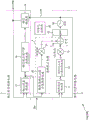
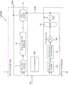
A CDR circuit of the first embodiment is illustrated in fig. 1. The CDR circuit 1 shown in the same drawing includes a frequency synchronization loop circuit 2, a phase synchronization loop circuit 3, a drift correction circuit 4, and a synchronization control unit 22.
The frequency synchronization loop circuit 2 synchronizes the frequency of the oscillation clock signal CLKf of the oscillation circuit (VCO)16 with the frequency of the input data Din. For example, the frequency error detector 11, the frequency correction value calculation holding circuit 12, the gain circuit 13, the adder 14, the DA converter (DAC)15 that converts a digital signal into an analog signal, and the oscillation circuit 16 composed of a Voltage Controlled Oscillator (VCO) are specifically exemplified, and the clock signal CLKf oscillated by the oscillation circuit 16 is fed back to the frequency error detector 11 to form a negative feedback loop as a whole. Each circuit may be a known circuit. For example, the frequency error detector 11 can count edge changes between the input data Din of a fixed pattern and the oscillation clock signal CLKf at regular intervals, such as 1 and 0 repeated, and detect a frequency error from the difference between the count values. The frequency correction value calculation holding circuit 12 has a digital filter function of integrating the frequency error to reduce a short-period signal component of the integrated value, a data latch function of holding a signal code generated by the digital filter function, and the like.
The data held in the frequency correction value calculation holding circuit 12 is provided with a necessary loop gain by a gain circuit 13, passed through an adder 14, and converted into an analog voltage signal by a DAC 15. The frequency correction calculation holding circuit 12 and the gain circuit 13 may be integrally configured by a digital filter.
The VCO16 has a varactor diode, and outputs a clock signal CLKf at an oscillation frequency corresponding to a change in electrostatic capacitance generated by an analog voltage signal applied to the varactor diode. When the frequency pulling operation of the clock signal CLKf of the frequency synchronization loop circuit 2 (operation of matching the frequency of the clock signal CLKf with the frequency of the input data Din) is considered, a relatively large (high) loop gain required to obtain the necessary negative feedback responsiveness is set in the gain circuit 13. A high loop gain is equivalent to a wide loop bandwidth, and can improve the response to the oscillation frequency variation of the VCO 16.
The phase synchronization loop circuit 3 inputs the oscillation clock signal CLKf to generate a clock signal CLKfp (phase synchronization clock signal CLKfp) synchronized with the phase of the input data Din. For example, with the phase error detector 17, the phase correction value calculation holding circuit 18, and the phase interpolator 19 specifically illustrated, the clock signal CLKfp corrected by the phase interpolator 19 is fed back to the phase error detector 17, constituting a negative feedback loop as a whole. For each circuit, a known circuit may be used. For example, the phase error detector 17 can be configured by a so-called digital phase comparator that outputs a voltage (phase difference voltage) corresponding to the phase difference. The phase correction value calculation holding circuit 18 has a digital filter function of integrating the phase difference voltage to reduce a short-period signal component of the integrated value, a data latch function of holding a signal code generated by the digital filter function, and the like.
The phase interpolator 19 adjusts the phase lead/lag of the clock signal CLKf in accordance with the signal code held in the phase correction value calculation holding circuit 18 to output the clock signal CLKfp, and performs phase pulling for optimizing the phase of the clock signal CLKfp to be synchronized with the timing of the edge of the input data Din.
The drift correction circuit 4 is a drift correction circuit configured as follows: in a phase pulling operation by the phase synchronization loop circuit 3 after the frequency pulling by the frequency synchronization loop circuit 2 or after the phase pulling is completed, a correction value is calculated based on a phase difference between the input data Din and the clock signal CLKfp, and the oscillation frequency of the oscillation circuit 16 can be corrected by the correction value with a smaller loop gain than the frequency synchronization loop circuit 2. For example, the frequency drift correction value calculation holding circuit 20, the gain circuit 21 having a lower gain than the gain circuit 13, and the adder 14 are specifically exemplified. The frequency drift correction value calculation holding circuit 20 has a digital filter function of reducing a signal component for a short period of an integrated value obtained by integrating the phase difference voltage from the phase error detector 17, a data latch function of determining whether or not the integrated value generated by the digital filter function exceeds a predetermined threshold value, and holding code data of the integrated value when the integrated value exceeds the predetermined threshold value, and the like.
The code data held at the frequency drift correction value calculation holding circuit 20 is given a comparatively low loop gain by the gain circuit 21 and is supplied to the adder 14. At this time, a signal code for obtaining the frequency of the clock signal CLKf of which the frequency pulling is completed is supplied to the adder 14 via the gain circuit 13, and the frequency of the clock signal CLKf changes in accordance with the output of the gain circuit 13 by adding the output of the gain circuit 21 of which the loop gain is low to the output of the gain circuit 13 of which the loop gain is high. The frequency drift correction value calculation holding circuit 20 and the low gain circuit 21 may be integrally configured by a digital filter.
For the change in the frequency of the clock signal CLKf caused by the drift correction circuit 4 with the purpose of compensating for the amount of fluctuation of the clock signal CLK caused by the temperature change, the magnitude of the code data output by the frequency drift correction value calculation holding circuit 20 and the loop gain provided by the gain circuit 21 are determined in response to this purpose. In short, the responsiveness of the output of the low gain circuit 21 to frequency fluctuations of the VCO16 is delayed.
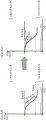
For example, when the continuous operation time of the CDR circuit becomes long, the output frequency of the VCO16 drifts due to temperature change. While the clock signal CLKfp can be corrected by the phase correction of the phase synchronization loop circuit 3 during a period in which the drift amount is small, the clock signal CLKfp cannot be corrected completely, that is, the frequency lock deviation cannot be corrected when the phase correction becomes large. As illustrated in fig. 5, if it is assumed that the frequency of the VCO16 is currently decreased with a temperature change, the oscillation frequency of the VCO16 is decreased as it is without correction, and the frequency lock is deviated at a certain time. The drift correction circuit 4 is a drift correction circuit that corrects the data supplied to the DAC 15 so as not to be equal to or lower than a given value when the oscillation frequency of the VCO16 decreases to the given value. Thereby, the frequency lock of the temporary pulled clock signal CLKf is not shifted.
Fig. 2 illustrates a system configuration in a case where the CDR circuit 1 of fig. 1 is applied to a data interface, and particularly shows a specific example of the synchronization control section 22 in the CDR circuit 1.
The system illustrated in fig. 2 becomes: the host device 100 is connected to a device including a control interface 101, a data interface 102, a processing controller 103, and a processing circuit 104, the control interface 101 inputs a command issued by the host device 100, the data interface 102 inputs data output by the host device 100, the processing controller 103 decodes the command, and the processing controller 103 causes the processing circuit 104 to process the input data in accordance with the result of the decoding.
The data interface 102 is configured as a so-called clock embedded type interface by the CDR circuit 1 and the sampling circuit 5. The sampling circuit 5 takes in the input data Din in synchronization with the clock signal CLKfp generated by the CDR circuit 1 and supplies it to the process controller 103.
The synchronization control unit 22 controls each operation of frequency pulling (frequency locking) by the frequency lock detector 23, phase pulling (phase locking) by the phase lock detector 24, and frequency correction by the drift correction circuit 4.φ 1 is an operation instruction signal of the frequency error detector 11, φ 2 is a frequency lock completion notification signal, φ 3 is an instruction signal for the detection operation of the phase error detector 17, φ 4 is a phase lock completion notification signal, and φ 5 is an instruction signal for the operation of the frequency drift correction value calculation holding circuit 20.
The synchronization control unit 22 controls each operation of frequency pulling (frequency locking) by the frequency lock detector 23, phase pulling (phase locking) by the phase lock detector 24, and frequency correction by the drift correction circuit 4.
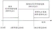
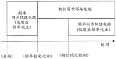
Fig. 3 illustrates a basic control method for the CDR circuit 1 by the synchronization control unit 22. The frequency correction operation by the frequency lock detector 23, i.e., the frequency pulling (frequency locking) operation of the clock signal CLKf, is initially started. The input data Din used for this operation is limited to have a specific data pattern such as 1 and 0 repetitions in the present embodiment. Thus, when the frequency lock is detected, the phase correction operation by the phase lock detector 24, that is, the phase pulling (phase locking) operation is started this time. The initial phase pulling motion may also use a specific pattern of input data Din as well as a frequency pulling motion, and may also use a different training pattern. After the phase lock is detected by the phase correction operation, the frequency drift correction by the drift correction circuit 4 is started. The frequency correction of the clock signal CLKf by the drift correction circuit 4 may be performed in parallel with the phase correction operation after the phase locking, or may be performed in a state in which the phase correction operation is stopped after the phase locking.
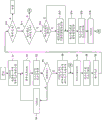
Fig. 4 illustrates an operation flow of the CDR circuit 1. First, when the process controller 103 gives an instruction to activate (ON) the CDR circuit 1 in response to a command from the host device 100, the synchronization control unit 22 activates the VCO16, operates the frequency error detector 11 in response to the signal Φ 1, and so ON, thereby enabling the frequency synchronization loop circuit 2 to operate and starting the input of the data Din (S1). Thus, the frequency error detector 11 detects an error between the input data Din and the frequency of the oscillation clock signal CLKf of the VCO16 (S2), the frequency correction value calculation holding circuit 12 calculates and holds a correction value based on the detected error (S3), determines whether the oscillation frequency CLKf is locked (S4), and reflects the correction value to the VCO16 if the oscillation frequency CLKf is unlocked (S5). The processing from S2 to S5 is repeated until frequency lock is determined. When the frequency lock of the clock signal CLKf is determined, the setting of the VCO16 is fixed, the frequency error detection by the frequency synchronization loop circuit 2 is ended by the signal Φ 2, the phase synchronization loop circuit 3 is started up this time (S6), and the phase error detection by the phase error detector 17 is started by the signal Φ 3 (S7). Thus, the phase correction value calculation holding circuit 18 calculates the correction value based on the phase difference between the input data Din and the clock signal CLKfp, and holds the calculated correction value (S8). The phase of the input clock signal CLKf is corrected by the held correction value and reflected to the clock signal CLKfp (S9).
Thereafter, it is determined whether all the input data Din have been received completely (S10), and if not, it is determined whether the phase of the clock signal CLKfp matches the phase of the input data Din and is phase-locked or whether phase-locking has been completed (S11), and if not, it returns to step S7 and the processing in steps S7 to S11 is repeated until phase-locking has been completed. The input data Din is changed from a specific fixed pattern for band pulling to original communication data at a predetermined timing when at least the predicted time for completing the frequency locking has elapsed.
When the phase lock is performed by the phase locked loop circuit 3, the synchronization control unit 22 is notified of the phase lock by the signal Φ 4. If the notification is the notification of the initial phase lock (S12), the synchronization control unit 22 activates the frequency drift correction value calculation holding circuit 20 using the signal Φ 5 (S13), inputs the output of the phase error detector 17 (S14), calculates a correction value for correcting the frequency drift of the oscillation circuit 16 based on the accumulation of the phase difference when the phase variation exceeds the threshold value, and holds the correction value (S15). The oscillation frequency of the oscillation circuit 16 is corrected by the held correction value (S16).
After correcting the frequency of the clock signal CLKf, the phase synchronization loop circuit 3 and the drift circuit 4 are simultaneously activated, and the processes S7 to S11 for phase correction and the processes S14 to S16 for correcting the oscillation frequency are performed in parallel. The frequency drift correction circuit 4 is started up once, and then operates in parallel with the phase locked loop circuit after the start-up as shown in fig. 3. That is, although the flow chart illustrates the case where the drift correction and the phase correction are performed in series for simplifying the drawing, the drift correction circuit actually operates when the phase correction is performed after the drift correction. Since the drift correction circuit 4 has a slow response, the drift correction value is changed again after the phase correction has sufficiently converged. The processes S7 to S11 for phase correction and the correction processes S14 to S16 for the oscillation frequency of the VCO16 for frequency drift by the drift correction circuit 4 are repeated until the reception is completed.
According to the first embodiment, the following operational effects are exhibited.
(1) Since the oscillation frequency of the VCO16 is corrected by the drift correction circuit 4 having a smaller loop gain than the frequency synchronization loop circuit 2 after the completion of the phase pulling, it is possible to correct the frequency variation of the oscillation circuit in the frequency synchronization loop circuit without undesirably oscillating the phase synchronization loop even in the phase pulling operation. Even if an unexpected frequency fluctuation occurs in the oscillation circuit VCO16 due to a temperature change or the like, the frequency pulling operation using a specific pattern of the input data Din is not newly performed, and the oscillation clock signal CLKf can be synchronized with the input data Din.
(2) The drift correction circuit 4 calculates a frequency correction value based on the phase error detected by the phase synchronization loop circuit 3, and adds the frequency correction value to the frequency control data of the frequency synchronization loop circuit 2 by the adder 14 with a smaller loop gain than that of the frequency synchronization loop circuit 2, so that the correction value can be easily reflected to the frequency synchronization loop circuit 2.
(3) It is needless to say that the phase synchronization loop circuit 3 needs to perform phase pulling on an arbitrary pattern of input data, but it is not always necessary to perform frequency pulling on an arbitrary pattern as in the case of frequency pulling performed at a preceding stage. In this regard, the frequency detector 11 in the first embodiment aims to simplify the frequency synchronization loop circuit 2 and reduce power consumption by setting a specific fixed pattern such as 1 and 0 repeatedly as a frequency pulling target. On the premise of this, the drift correction circuit 4 can calculate the frequency drift by using the error detection function of the phase error detector 17 corresponding to an arbitrary pattern after the frequency pulling is completed.
(4) As explained in the flowchart of fig. 4, in the first embodiment, the oscillation frequency for which the frequency pulling is completed is corrected in the phase pulling completed state using the drift correction circuit 4 having a smaller loop gain than the frequency synchronization loop circuit 2, and therefore, it is possible to prevent the phase synchronization loop circuit 3 from performing excessive negative feedback control and the risk that the phase synchronization loop becomes unstable and correct the fluctuation of the oscillation frequency by frequency correction using the drift correction circuit 4 without fail.
< second embodiment >
An example of a CDR circuit using a drift correction circuit is described as a second embodiment.
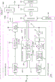
Fig. 6 illustrates a CDR circuit 1A according to a second embodiment. The CDR circuit 1A shown in the same drawing has a frequency synchronization loop circuit 2A and a phase synchronization loop circuit 3. The cross-phase synchronization loop circuit 3 and the drift correction circuit 4 of the frequency synchronization loop circuit 2 as employed in the first embodiment of fig. 1 are not used. In the second embodiment, the loop gain of the frequency synchronization loop circuit 2A can be made variable, so that the frequency synchronization loop circuit 2A also performs frequency correction for frequency drift of the VCO 16.
A specific example of the CDR circuit 1A of the second embodiment will be described. The difference from fig. 1 is the configuration of the frequency synchronization loop circuit 2A used in place of the drift correction circuit 4. That is, the frequency detection 11A is not only a specific fixed pattern in which 1 and 0 are repeated, but also a frequency error can be detected for an arbitrary pattern, and the circuit scale is larger than that of the frequency error detector 11. The frequency correction method is used for applications requiring frequency correction of various input patterns. Although not shown in the figure, a known circuit configuration using a counter or the like may be employed. In addition, the frequency synchronization loop circuit 2A employs a variable gain circuit 13A capable of variably switching the loop gain for the correction value held by the frequency correction value calculation holding circuit 12 instead of the fixed gain circuit 3, and the adder 14 is not used because the drift correction circuit 4 is not used. In the frequency pulling operation immediately after the start-up in the frequency synchronization loop circuit 2A, a high loop gain is set in the variable gain circuit 13A so that the error by the frequency error detector 11A can be reflected in the oscillation frequency of the VCO16 with relatively high responsiveness. After the phase pulling after the frequency pulling is completed, a low loop gain is set to the variable gain circuit 13A so that the error by the frequency error detector 11A can be reflected to the oscillation frequency of the VCO16 with relatively low responsiveness. It is sufficient that the frequency can be corrected in a direction to compensate for the oscillation frequency variation (frequency drop) of the VCO16 caused by temperature change or the like, because conversely if there is a slight variation to respond sensitively, the phase synchronization is deviated and the frequency of the clock signal CLKfp becomes unstable. This case is the same as the first embodiment. The synchronization control unit 20A performs switching control of the loop gain in the frequency synchronization loop circuit according to the synchronization operation of the oscillation clock, and performs control of the frequency synchronization loop circuit and control of the phase synchronization loop circuit 3 in the same manner as described above. Note that the same reference numerals are assigned to circuit blocks that realize the same functions as those in fig. 1, and detailed description thereof is omitted.
Fig. 7 illustrates a system configuration in a case where the CDR circuit 1A of fig. 6 is applied to a data interface. The system illustrated in fig. 7 becomes: the host device 100 is connected to a device including a control interface 101, a data interface 102A, a processing controller 103, and a processing circuit 104, the control interface 101 inputs a command issued by the host device 100, the data interface 102A inputs data output by the host device 100, the processing controller 103 interprets the command, and the processing controller 103 causes the processing circuit 104 to process the input data in accordance with the interpretation result.
The data interface 102A is configured as a so-called clock embedded type interface by the CDR circuit 1A and the sampling circuit 5. The sampling circuit 5 takes in the input data Din in synchronization with the clock signal CLKfp generated by the CDR circuit 1A and supplies it to the process controller 103.
The synchronization control section 22A in the CDR circuit 1A has a frequency lock detector 23A and a phase lock detector 24A. The synchronization control unit 22A controls frequency pulling (frequency locking) by the frequency lock detector 23A, phase pulling (phase locking) by the phase lock detector 24, and switching of the loop gain. Phi 11 is an operation instruction signal for the frequency error detector 11A, phi 12 is a completion notification signal for frequency locking, phi 13 is an instruction signal for the detection operation of the phase error detector 17, phi 14 is a completion notification signal for phase locking, and phi 15 is a switching signal for the loop gain of the variable gain circuit 13A. The same reference numerals are given to circuit blocks having the same functions as those in fig. 2, and detailed description thereof is omitted.
Fig. 8 illustrates a basic control method for the CDR circuit 1A by using the synchronization control unit 22A. The frequency correction operation by the frequency lock detector 23A, i.e., the frequency pulling (frequency locking) operation of the clock signal CLKf, is initially started. The input data Din used for this operation has an arbitrary data pattern, unlike the first embodiment. Thus, when the frequency lock is detected, the phase correction operation by the phase lock detector 24A, that is, the phase pulling (phase locking) operation is started this time. The phase pulling operation is also performed on the input data Din having an arbitrary pattern, similarly to the frequency pulling operation. When phase lock is detected by the phase correction operation, the phase lock detector 24A switches the loop gain of the variable gain circuit 13A to low, and the frequency synchronization loop circuit 2A has a low loop gain and corrects the oscillation clock signal of the VCO16 for variations. The drift correction of the VCO16 by the frequency synchronization loop circuit 2A at the low loop gain is performed after the initial phase locking, and the drift correction is performed after the initial phase locking in parallel with the phase correction operation of the phase synchronization loop circuit 3. Alternatively, the frequency synchronization loop circuit 2A may be started at the same time when the phase synchronization loop circuit 3 is started.
Fig. 9 illustrates an operation flow of the CDR circuit 1A. First, when the process controller 103 gives an instruction to activate (ON) the CDR circuit 1A in accordance with an instruction from the host device 100, the synchronization control unit 22A activates the VCO16, operates the frequency error detector 11A with the signal Φ 1, and the like, thereby operating the frequency synchronization loop circuit 2A and starting inputting of the data Din (S21). Thus, the frequency error detector 11A detects an error between the input data Din and the frequency of the oscillation clock signal CLKf of the VCO16 (S22), the frequency correction value calculation holding circuit 12 calculates and holds a correction value based on the detected error (S23), determines whether the oscillation frequency CLKf is locked (S24), and reflects the correction value to the VCO16 if the oscillation frequency CLKf is unlocked (S25). The processing from S22 to S25 is repeated until frequency lock is determined. When the frequency lock of the clock signal CLKf is determined, the setting of the VCO16 is fixed, the frequency error detection by the frequency synchronization loop circuit 2A is ended by the signal Φ 2, the phase synchronization loop circuit 3 is started this time (S26), the phase error detection by the phase error detector 17 is started by the signal Φ 3 (S27), the correction value is calculated by the phase correction value calculation holding circuit 18 based on the phase difference between the input data Din and the clock signal CLKfp, and the calculated correction value is held (S28). The phase of the clock signal CLKf is corrected by the held correction value, and is reflected to the clock signal CLKfp (S29).
Thereafter, it is determined whether or not all of the input data Din have been received (S30), and if not, it is determined whether or not the phase of the clock signal CLKfp matches the phase of the input data Din and is phase-locked, or whether or not the phase locking has been completed (S31), and if not, it returns to step S27, and the processing of steps S27 to S31 is repeated until the phase is locked. The reception completion judgment is made by the process controller 103.
When the phase lock is performed by the phase locked loop circuit 3, the signal Φ 4 notifies the synchronization control unit 22A of the phase lock. If the notification is the notification of the initial phase lock (S32), the synchronization control section 22A starts the frequency drift correction mode for the frequency synchronization loop circuit 2A using the signal Φ 15 (S33). That is, the loop gain of the variable gain circuit 13A is switched from high gain to low gain by the signal Φ 15, and the frequency synchronization loop circuit 2A is operated. Thus, the frequency correction value calculation holding circuit 12 receives the frequency error detected by the frequency error detector 11A (S34), and based on the received error, the frequency correction value calculation holding circuit 12 calculates and holds a correction value for correcting the frequency drift of the oscillation circuit 16 (S35). With respect to the held correction value, the oscillation frequency of the oscillation circuit 16 is corrected with a low loop gain (S36).
After the frequency of the clock signal CLKf is corrected, the phase synchronization loop circuit 3 is used again to perform the processes S27 to S31 for phase correction, and after the phase correction, the processes S34 to S36 for correcting the frequency drift of the VCO16 are performed again. These processes are repeated until the reception is completed.
According to the second embodiment, the following operational effects are exhibited.
(1) Since the frequency pulling operation is performed in a state where the loop gain of the frequency synchronization loop circuit 2A having completed pulling is switched to a small loop gain, it is possible to correct the frequency variation of the VCO16 in the frequency synchronization loop circuit 2A even in the phase pulling operation when the oscillation is not undesirably performed by the phase synchronization loop. Even if an unexpected frequency fluctuation occurs in the VCO16 due to a temperature change or the like, the clock signal CLKf can be synchronized with the input data without newly performing the frequency pulling operation using the input data pattern.
(2) The frequency synchronization loop circuit 2A can easily switch the loop gain of the frequency synchronization loop by the variable gain circuit 13A.
(3) Since the frequency synchronization loop circuit 2A performs the frequency pulling operation on an arbitrary pattern of the input data Din, the configuration of the frequency synchronization loop circuit 2A becomes complicated as compared with the case of performing the frequency pulling operation in a fixed pattern as in the first embodiment, but a new loop circuit such as the drift correction circuit 4 is not required to be newly provided, and the frequency drift of the VCO16 can be dealt with.
(4) Since the oscillation frequency of the VCO16, which has completed pulling, is corrected in the phase pulling completed state using the frequency synchronization loop circuit 2A switched to a small loop gain, it is possible to correct the frequency drift of the VCO16 without the risk of the phase synchronization loop becoming unstable.
< third embodiment >
As a third embodiment, a liquid crystal driver is illustrated in fig. 10 as a semiconductor device including a CDR circuit in an external interface circuit. The liquid crystal driver (LCD driver) 106 constitutes an LCD module (or LCD panel) 108 together with a liquid crystal display (LCD _ DSP)120 and a power supply circuit 121 formed on a glass substrate.
The liquid crystal driver (LCD driver) 106 has a control interface 101 and a data interface 102(102A) for inputting image data as an external interface circuit connected to the host apparatus (HST) 100. A command is supplied from the host device 100 via the control interface circuit 101, and display data is supplied via the data interface 102 (102A). The CDR circuit 1(1A) is applied to the data interface 102(102A), and a so-called clock embedded data interface is configured. As a processing circuit 106 which processes a command supplied to the control interface 101 and image data supplied to the data interface 102(102A), there are provided a display controller 103, a memory 110, a gradation voltage controller 111, a source driver 112, and a gate control driver 113 as processing controllers. The display controller 103 uses the interpretation result of the supplied command and the command parameter to control the inside, and saves the supplied display data to the memory 110. The gray scale voltage controller 111 generates a plurality of gray scale voltages, selects the gray scale voltages in pixel units in accordance with display data in display line units supplied from the memory 110 in synchronization with display timing, and supplies the selected gray scale voltages to the source driver 112. The display controller 103 sequentially selects and drives the gate lines of the liquid crystal display 120 for each display frame in synchronization with the horizontal scanning period using the gate control driver 113 during the display operation. In addition, the display controller 103 supplies display data (display line data) for one gate line from the memory 110 to the grayscale voltage controller 111 in synchronization with the horizontal scanning period, and selects a grayscale voltage for each pixel of the data using the supplied display line data. The selected gray voltages are supplied to a plurality of driving amplifiers constituting the source driver 112. The plurality of driving amplifiers drives the plurality of source lines of the liquid crystal display 120 in parallel in units of display line data.
Since the CDR circuit 1(1A) is applied to the data interface 102(102A), the reliability of the so-called clock embedded data interface in the LCD driver 106 can be improved. Even if a drop in oscillation frequency occurs due to a temperature rise of the VCO16, the fluctuation amount can be corrected by frequency correction of the oscillation clock signal CLKf of the VCO 16. In this correction, it is not required to stop the input of the input data Din to resume the clock synchronization from the frequency pulling.
Although the invention made by the present inventors has been specifically described above based on the embodiments, it goes without saying that the invention is not limited to this invention, and various modifications can be made without departing from the scope of the invention.
The present invention is not limited to the LCD driver, and can be widely applied to semiconductor devices and systems provided with a clock-embedded interface. The configurations of the frequency synchronization loop circuit and the phase synchronization loop circuit are not limited to the above-described embodiments, and can be appropriately modified. The setting and switching of the loop gain are not limited to the above embodiments, and can be performed by various means such as a digital filter.
Description of reference numerals
1. 1A: a CDR circuit; 2. 2A: a frequency synchronization loop circuit; 3: a phase synchronization loop circuit; 4: a drift correction circuit; din: inputting data; 11. 11A: a frequency error detector; 12: a frequency correction value calculation holding circuit; 13. 13A: a gain circuit; 14: an addition circuit; 15: a DA converter (DAC); 16: an oscillation circuit (VCO); CLKf: an oscillating clock signal of the frequency synchronization loop circuit; CLKfp: a clock signal output from the phase synchronization loop circuit; 17: a phase error detection circuit; 18: a phase correction value calculation holding circuit; 19: a phase interpolator; 20: a frequency drift correction value calculation holding circuit; 21: a low loop gain circuit; 22: a synchronization control unit; 101: a control interface; 102. 102A: a data interface; 103: a process controller; 104: a processing circuit; 106: a liquid crystal driver (LCD driver); 108: an LCD module (or LCD panel); 100: a host device (HST); 110: a memory; 111: a gray scale voltage controller; 112: a source driver; 113: a gate control driver; 120: liquid crystal display (LCD _ DSP).
Claims (15)
1. A CDR circuit having:
a frequency synchronization loop circuit that synchronizes a frequency of an oscillation clock signal of the oscillation circuit with a frequency of the input data;
a phase synchronization loop circuit that inputs the oscillation clock signal and outputs a phase synchronization clock signal synchronized with a phase of the input data; and
and a drift correction circuit configured to calculate a correction value based on a phase difference between the input data and the phase-synchronized clock signal during a phase pulling operation by the phase-synchronized loop circuit after the frequency pulling by the frequency-synchronized loop circuit or after the phase pulling is completed, and to correct an oscillation frequency of the oscillation circuit with the correction value with a smaller loop gain than that of the frequency-synchronized loop circuit.
2. The CDR circuit of claim 1,
the drift correction circuit calculates a frequency correction value based on the phase error detected by the phase synchronization loop circuit, and adds the correction value to frequency control data of the frequency synchronization loop circuit with a smaller loop gain than the frequency synchronization loop circuit.
3. The CDR circuit of claim 2,
the frequency synchronization loop circuit performs a frequency pulling action on a specific fixed pattern of input data,
the phase locked loop circuit performs phase pulling on an arbitrary pattern of input data.
4. The CDR circuit of claim 2,
the control unit is provided with a control unit for managing the following controls: the method includes instructing a start of a phase pulling operation to the phase synchronization loop circuit in response to a notification of completion of the frequency pulling in the frequency synchronization loop circuit, instructing an operation of the frequency correction value to the drift correction circuit in response to the notification of completion of the phase pulling, and adding the correction value to frequency control data of the frequency synchronization loop circuit with a smaller loop gain than the frequency synchronization loop circuit to instruct the phase synchronization loop circuit again of the start of the phase pulling operation when the operated correction value reaches a prescribed value.
5. A CDR circuit having:
a frequency synchronization loop circuit that synchronizes a frequency of an oscillation clock signal of the oscillation circuit with a frequency of the input data; and
a phase synchronization loop circuit that inputs the oscillation clock signal and outputs a phase synchronization clock signal synchronized with a phase of the input data,
the frequency synchronization loop circuit performs a frequency pulling operation in a state where a loop gain is switched to be small, in parallel with a phase pulling operation of the phase synchronization loop circuit after the frequency pulling operation or after the phase pulling operation is completed.
6. The CDR circuit of claim 5,
the frequency synchronization loop circuit has a variable gain circuit capable of variably switching a loop gain.
7. The CDR circuit of claim 5,
the frequency synchronization loop circuit performs a frequency pulling action on an arbitrary pattern of input data,
the phase synchronization loop circuit performs phase synchronization on an arbitrary pattern of input data.
8. The CDR circuit of claim 6,
the control unit is provided with the following control: the start of the phase pulling action is indicated to the phase synchronization loop circuit in response to a notification of completion of the frequency pulling in the frequency synchronization loop circuit, and the start of the frequency pulling action is indicated by switching the loop gain of the frequency synchronization loop circuit to be small in response to the notification of completion of the phase pulling, and the start of the phase pulling action is again indicated to the phase synchronization loop circuit after the frequency pulling is completed.
9. A semiconductor device comprising an external interface circuit and a processing circuit that processes data supplied to the external interface circuit, the external interface circuit being provided with the CDR circuit according to claim 1 as a circuit that inputs the data.
10. The semiconductor device as set forth in claim 9,
the processing circuit inputs image data supplied to the CDR circuit, and outputs a gradation voltage corresponding to the input image data in pixel units in synchronization with a display timing.
11. A CDR circuit comprising a synchronizing circuit that forms a frequency synchronization loop that synchronizes a frequency of an oscillation clock signal of an oscillation circuit with a frequency of input data and a phase synchronization loop that inputs the oscillation clock signal to generate a phase synchronization clock signal synchronized with a phase of the input data, wherein in the CDR circuit,
the synchronization circuit has the following circuits: the circuit updates the oscillation frequency of the completion of pulling with a smaller loop gain than the frequency synchronization loop for the frequency of the completion of frequency pulling using the frequency synchronization loop circuit during or after the completion of the phase pulling using the phase synchronization loop.
12. The CDR circuit of claim 11,
the circuit for updating the oscillation frequency is a drift correction circuit configured as follows: in a phase pulling operation by the phase synchronization loop after the frequency pulling by the frequency synchronization loop or after the phase pulling is completed, a correction value is calculated based on a phase difference between the input data and the phase synchronization clock signal, and the oscillation frequency variation of the oscillation circuit can be corrected by the correction value with a smaller loop gain than that of the frequency synchronization loop.
13. The CDR circuit of claim 12,
the control unit is provided with the following control: the start of a phase pulling operation is instructed to the phase synchronization loop circuit in response to a notification of completion of the frequency pulling in the frequency synchronization loop circuit, the operation of the frequency correction value is instructed to the drift correction circuit in response to the notification of completion of the phase pulling, and when the calculated frequency correction value reaches a predetermined value, the loop gain is lowered, the frequency correction value is added to the frequency control data of the frequency synchronization loop circuit, and the start of the phase pulling operation is instructed to the phase synchronization loop circuit again.
14. The CDR circuit of claim 11,
the circuit that updates the oscillation frequency is a variable gain circuit that is arranged in the frequency synchronization loop circuit and is capable of variably switching the loop gain,
the variable gain circuit switches the loop gain to be small in parallel with the phase pulling operation of the phase locked loop circuit after the frequency pulling operation, or switches the loop gain to be small after the completion of the phase pulling operation.
15. The CDR circuit of claim 14,
the control unit is provided with the following control: the start of the phase pulling operation is instructed to the phase synchronization loop circuit in response to a notification of completion of the frequency pulling in the frequency synchronization loop circuit, the start of the frequency pulling operation is instructed to the frequency synchronization loop circuit by switching the loop gain to be small in response to the notification of completion of the phase pulling, and the start of the phase pulling operation is instructed to the phase synchronization loop circuit again after the frequency pulling is completed.
Applications Claiming Priority (2)
| Application Number | Priority Date | Filing Date | Title |
|---|---|---|---|
| JP2014144119A JP6430738B2 (en) | 2014-07-14 | 2014-07-14 | CDR circuit and semiconductor device |
| JP2014-144119 | 2014-07-14 |
Publications (2)
| Publication Number | Publication Date |
|---|---|
| CN105262483A CN105262483A (en) | 2016-01-20 |
| CN105262483B true CN105262483B (en) | 2020-12-11 |
Family
ID=55068387
Family Applications (1)
| Application Number | Title | Priority Date | Filing Date |
|---|---|---|---|
| CN201510410326.6A Active CN105262483B (en) | 2014-07-14 | 2015-07-14 | CDR circuit and semiconductor device |
Country Status (3)
| Country | Link |
|---|---|
| US (1) | US9413517B2 (en) |
| JP (1) | JP6430738B2 (en) |
| CN (1) | CN105262483B (en) |
Families Citing this family (19)
| Publication number | Priority date | Publication date | Assignee | Title |
|---|---|---|---|---|
| JP2016021629A (en) * | 2014-07-14 | 2016-02-04 | シナプティクス・ディスプレイ・デバイス合同会社 | Cdr(clock data recovery) circuit and semiconductor device |
| JP6536347B2 (en) * | 2015-10-20 | 2019-07-03 | 富士通株式会社 | Frequency detection method |
| US9843439B2 (en) * | 2016-01-27 | 2017-12-12 | Ciena Corporation | System and method for managing holdover |
| US10348414B2 (en) * | 2016-06-30 | 2019-07-09 | Avago Technologies International Sales Pte. Limited | Clock-and-data recovery (CDR) circuitry for performing automatic rate negotiation |
| KR102480913B1 (en) | 2016-07-11 | 2022-12-26 | 삼성전자주식회사 | Method for transmitting data and electronic device thereof |
| CN107800427B (en) * | 2016-09-05 | 2021-04-06 | 创意电子股份有限公司 | Clock data recovery module |
| CN106712768A (en) * | 2016-12-12 | 2017-05-24 | 深圳市紫光同创电子有限公司 | Deburring frequency locking circuit |
| KR102633143B1 (en) * | 2016-12-23 | 2024-02-02 | 삼성전자주식회사 | Automatic frequency controller for adjusting digital loop filter gain based on wireless channel classification, wireless communication device including the same, automatic frequency controlling method, and wireless communicating method |
| CN107682007B (en) * | 2017-09-22 | 2021-01-15 | 哈尔滨工业大学 | Fast locking low-jitter clock data recovery circuit based on double loops |
| CN107911113B (en) * | 2017-10-31 | 2021-01-12 | 北京集创北方科技股份有限公司 | Clock data recovery circuit, loop bandwidth adjusting method thereof and processor |
| CN108199710B (en) * | 2017-12-25 | 2021-06-29 | 深圳市紫光同创电子有限公司 | Oscillator correction circuit and oscillator correction method |
| US11349485B2 (en) * | 2019-01-28 | 2022-05-31 | Mediatek Inc. | Clock and data recovery and associated signal processing method |
| CN111435827B (en) * | 2020-01-14 | 2023-11-28 | 珠海市杰理科技股份有限公司 | Quick oscillation starting circuit, method, crystal oscillator and integrated chip |
| US11038602B1 (en) | 2020-02-05 | 2021-06-15 | Credo Technology Group Limited | On-chip jitter evaluation for SerDes |
| US10992501B1 (en) | 2020-03-31 | 2021-04-27 | Credo Technology Group Limited | Eye monitor for parallelized digital equalizers |
| KR20210129327A (en) * | 2020-04-20 | 2021-10-28 | 주식회사 엘엑스세미콘 | Data driving device and method for driving the same |
| US10892763B1 (en) * | 2020-05-14 | 2021-01-12 | Credo Technology Group Limited | Second-order clock recovery using three feedback paths |
| US11855648B2 (en) | 2022-01-14 | 2023-12-26 | Samsung Display Co., Ltd. | Clock pattern detection and correction |
| CN115985221B (en) * | 2023-03-21 | 2023-07-21 | 深圳通锐微电子技术有限公司 | Source driver, bandwidth adjusting method and display panel |
Citations (5)
| Publication number | Priority date | Publication date | Assignee | Title |
|---|---|---|---|---|
| JPS62253224A (en) * | 1986-01-14 | 1987-11-05 | Toshiba Corp | Phase synchronizing circuit |
| JPH01293718A (en) * | 1988-05-20 | 1989-11-27 | Hitachi Ltd | Phase locked loop circuit |
| JP2005006187A (en) * | 2003-06-13 | 2005-01-06 | Renesas Technology Corp | Pll circuit |
| CN102820886A (en) * | 2012-08-10 | 2012-12-12 | 硅谷数模半导体(北京)有限公司 | Signal detection method, signal detection device and PLL (phase locked loop) and CDR system with device |
| JP2013005144A (en) * | 2011-06-15 | 2013-01-07 | Renesas Electronics Corp | Serial-parallel conversion circuit, clock data recovery circuit, drive circuit for display device, and serial-parallel conversion method |
Family Cites Families (13)
| Publication number | Priority date | Publication date | Assignee | Title |
|---|---|---|---|---|
| JPH08331118A (en) * | 1995-06-02 | 1996-12-13 | Yupiteru Ind Co Ltd | Method and device for reference clock regeneration of digital radio telephone system |
| JP2000243042A (en) * | 1999-02-19 | 2000-09-08 | Matsushita Electric Ind Co Ltd | Clock recovery device |
| JP2002198805A (en) * | 2000-12-22 | 2002-07-12 | Asahi Kasei Microsystems Kk | Pll circuit |
| US6753711B2 (en) * | 2002-06-26 | 2004-06-22 | Comtech Ef Data | Digital summing phase-lock loop circuit with sideband control and method therefor |
| NZ524537A (en) * | 2003-03-04 | 2005-08-26 | Tait Electronics Ltd | Improvements relating to frequency and/or phase lock loops |
| US6803827B1 (en) * | 2003-04-09 | 2004-10-12 | Analog Devices, Inc. | Frequency acquisition system |
| JP3939715B2 (en) * | 2004-08-20 | 2007-07-04 | 日本テキサス・インスツルメンツ株式会社 | Phase-locked loop circuit |
| US7327195B2 (en) * | 2004-08-27 | 2008-02-05 | Matsushita Electric Industrial Co., Ltd. | PLL frequency synthesizer |
| US7932784B1 (en) * | 2005-03-17 | 2011-04-26 | Rf Micro Devices, Inc. | Frequency and phase locked loop synthesizer |
| TWI346460B (en) * | 2006-10-31 | 2011-08-01 | Realtek Semiconductor Corp | A clock and data recovery circuit and a method for adjusting loop bandwidth used thereby |
| US20090108891A1 (en) * | 2007-10-26 | 2009-04-30 | Matsushita Electric Industrial Co., Ltd. | Bandwidth control in a mostly-digital pll/fll |
| JP2012044446A (en) | 2010-08-19 | 2012-03-01 | Renesas Electronics Corp | Clock data recovery circuit |
| JP2012049863A (en) * | 2010-08-27 | 2012-03-08 | Renesas Electronics Corp | Semiconductor device |
-
2014
- 2014-07-14 JP JP2014144119A patent/JP6430738B2/en active Active
-
2015
- 2015-07-09 US US14/795,494 patent/US9413517B2/en active Active
- 2015-07-14 CN CN201510410326.6A patent/CN105262483B/en active Active
Patent Citations (5)
| Publication number | Priority date | Publication date | Assignee | Title |
|---|---|---|---|---|
| JPS62253224A (en) * | 1986-01-14 | 1987-11-05 | Toshiba Corp | Phase synchronizing circuit |
| JPH01293718A (en) * | 1988-05-20 | 1989-11-27 | Hitachi Ltd | Phase locked loop circuit |
| JP2005006187A (en) * | 2003-06-13 | 2005-01-06 | Renesas Technology Corp | Pll circuit |
| JP2013005144A (en) * | 2011-06-15 | 2013-01-07 | Renesas Electronics Corp | Serial-parallel conversion circuit, clock data recovery circuit, drive circuit for display device, and serial-parallel conversion method |
| CN102820886A (en) * | 2012-08-10 | 2012-12-12 | 硅谷数模半导体(北京)有限公司 | Signal detection method, signal detection device and PLL (phase locked loop) and CDR system with device |
Also Published As
| Publication number | Publication date |
|---|---|
| US20160013929A1 (en) | 2016-01-14 |
| JP6430738B2 (en) | 2018-11-28 |
| US9413517B2 (en) | 2016-08-09 |
| JP2016021628A (en) | 2016-02-04 |
| CN105262483A (en) | 2016-01-20 |
Similar Documents
| Publication | Publication Date | Title |
|---|---|---|
| CN105262483B (en) | CDR circuit and semiconductor device | |
| CN101098220B (en) | Digital phase-locked loop based clock synchronization method and system thereof | |
| US7679453B2 (en) | Phase-locked loop capable of dynamically adjusting phase of output signal according to detection result of phase/frequency detector, and method thereof | |
| US7366271B2 (en) | Clock and data recovery device coping with variable data rates | |
| TWI449341B (en) | Signal transmission system and signal transmission method | |
| CN102629878B (en) | For the signal generator of reflector or receiver, reflector and receiver | |
| US8923468B2 (en) | Clock and data recovery circuit selectively configured to operate in one of a plurality of stages and related method thereof | |
| US9147376B2 (en) | Display device and method | |
| US20230246801A1 (en) | Clock and data recovery circuit and a display apparatus having the same | |
| KR20140109131A (en) | Display interface for compressing/decompressing image data, method thereo, and device including the same | |
| KR20080044977A (en) | Phase locked loop and method of operating phase locked loop | |
| US11728815B2 (en) | Semiconductor device | |
| KR102655530B1 (en) | Stream clock generator and embedded displayport system including the same | |
| CN105306049A (en) | Cdr circuit and semiconductor device | |
| US11424746B1 (en) | Reference-less clock and data recovery device and method | |
| US10483989B2 (en) | Phase-locked loop, phase-locking method, and communication unit | |
| JP2010081513A (en) | Signal processing apparatus and signal processing method | |
| JP2010081512A (en) | Signal processing apparatus and signal processing method | |
| US11646862B2 (en) | Reception device and transmission and reception system | |
| CN109818614B (en) | Time sequence control method, time sequence control chip and display device | |
| US7295821B2 (en) | Multiple base station automatic frequency control architecture in wireless communication system | |
| US20080151117A1 (en) | Horizontal synchronous circuit, display device, and clock adjusting method | |
| EP1265365A2 (en) | Frequency synchronous apparatus and frequency synchronous control method | |
| CN109391262B (en) | Clock recovery device and method | |
| CN114978159A (en) | CDR control loop frequency correction method, device, loop and receiver |
Legal Events
| Date | Code | Title | Description |
|---|---|---|---|
| C06 | Publication | ||
| PB01 | Publication | ||
| CB02 | Change of applicant information |
Address after: Tokyo, Japan, Japan Applicant after: Sin Knapp Dick J Japan Contract Society Address before: Tokyo, Japan, Japan Applicant before: Xin Napudikesi display contract commercial firm |
|
| COR | Change of bibliographic data | ||
| SE01 | Entry into force of request for substantive examination | ||
| SE01 | Entry into force of request for substantive examination | ||
| GR01 | Patent grant | ||
| GR01 | Patent grant |