CN103531600A - Radiation detection apparatus and method of manufacturing the same - Google Patents
Radiation detection apparatus and method of manufacturing the same Download PDFInfo
- Publication number
- CN103531600A CN103531600A CN201310270654.1A CN201310270654A CN103531600A CN 103531600 A CN103531600 A CN 103531600A CN 201310270654 A CN201310270654 A CN 201310270654A CN 103531600 A CN103531600 A CN 103531600A
- Authority
- CN
- China
- Prior art keywords
- sealant
- pel array
- base plate
- sensor base
- protective layer
- Prior art date
- Legal status (The legal status is an assumption and is not a legal conclusion. Google has not performed a legal analysis and makes no representation as to the accuracy of the status listed.)
- Pending
Links
- 230000005855 radiation Effects 0.000 title claims abstract description 76
- 238000004519 manufacturing process Methods 0.000 title claims abstract description 26
- 238000001514 detection method Methods 0.000 title abstract description 4
- 238000007789 sealing Methods 0.000 claims abstract description 22
- 239000000565 sealant Substances 0.000 claims description 117
- 239000010410 layer Substances 0.000 claims description 116
- 239000011241 protective layer Substances 0.000 claims description 52
- 238000005520 cutting process Methods 0.000 claims description 45
- 238000000034 method Methods 0.000 claims description 26
- 239000000463 material Substances 0.000 claims description 20
- 229920005989 resin Polymers 0.000 claims description 12
- 239000011347 resin Substances 0.000 claims description 12
- 230000015572 biosynthetic process Effects 0.000 claims description 9
- 239000013078 crystal Substances 0.000 claims description 6
- 239000000758 substrate Substances 0.000 abstract 3
- 239000002585 base Substances 0.000 description 59
- 238000012986 modification Methods 0.000 description 14
- 230000004048 modification Effects 0.000 description 14
- 238000005516 engineering process Methods 0.000 description 11
- 239000004925 Acrylic resin Substances 0.000 description 9
- 229920000178 Acrylic resin Polymers 0.000 description 9
- 238000003491 array Methods 0.000 description 8
- CURLTUGMZLYLDI-UHFFFAOYSA-N Carbon dioxide Chemical compound O=C=O CURLTUGMZLYLDI-UHFFFAOYSA-N 0.000 description 6
- 238000000151 deposition Methods 0.000 description 6
- 230000008021 deposition Effects 0.000 description 6
- 229920005992 thermoplastic resin Polymers 0.000 description 6
- 239000004642 Polyimide Substances 0.000 description 5
- 239000011248 coating agent Substances 0.000 description 5
- 238000000576 coating method Methods 0.000 description 5
- 229920001721 polyimide Polymers 0.000 description 5
- 238000010586 diagram Methods 0.000 description 4
- 230000002285 radioactive effect Effects 0.000 description 4
- 229910052782 aluminium Inorganic materials 0.000 description 3
- 239000004411 aluminium Substances 0.000 description 3
- XAGFODPZIPBFFR-UHFFFAOYSA-N aluminium Chemical compound [Al] XAGFODPZIPBFFR-UHFFFAOYSA-N 0.000 description 3
- 229910002092 carbon dioxide Inorganic materials 0.000 description 3
- 239000001569 carbon dioxide Substances 0.000 description 3
- 230000005611 electricity Effects 0.000 description 3
- 239000003822 epoxy resin Substances 0.000 description 3
- 229910052751 metal Inorganic materials 0.000 description 3
- 239000002184 metal Substances 0.000 description 3
- 238000005498 polishing Methods 0.000 description 3
- 229920000647 polyepoxide Polymers 0.000 description 3
- 229920005644 polyethylene terephthalate glycol copolymer Polymers 0.000 description 3
- 238000002360 preparation method Methods 0.000 description 3
- 239000002390 adhesive tape Substances 0.000 description 2
- 210000000481 breast Anatomy 0.000 description 2
- XQPRBTXUXXVTKB-UHFFFAOYSA-M caesium iodide Chemical compound [I-].[Cs+] XQPRBTXUXXVTKB-UHFFFAOYSA-M 0.000 description 2
- 238000006243 chemical reaction Methods 0.000 description 2
- 229920001971 elastomer Polymers 0.000 description 2
- 239000011521 glass Substances 0.000 description 2
- 229920001296 polysiloxane Polymers 0.000 description 2
- 239000011734 sodium Substances 0.000 description 2
- FVAUCKIRQBBSSJ-UHFFFAOYSA-M sodium iodide Chemical class [Na+].[I-] FVAUCKIRQBBSSJ-UHFFFAOYSA-M 0.000 description 2
- 235000009518 sodium iodide Nutrition 0.000 description 2
- 239000002904 solvent Substances 0.000 description 2
- XLYOFNOQVPJJNP-UHFFFAOYSA-N water Substances O XLYOFNOQVPJJNP-UHFFFAOYSA-N 0.000 description 2
- 108010022579 ATP dependent 26S protease Proteins 0.000 description 1
- DGAQECJNVWCQMB-PUAWFVPOSA-M Ilexoside XXIX Chemical compound C[C@@H]1CC[C@@]2(CC[C@@]3(C(=CC[C@H]4[C@]3(CC[C@@H]5[C@@]4(CC[C@@H](C5(C)C)OS(=O)(=O)[O-])C)C)[C@@H]2[C@]1(C)O)C)C(=O)O[C@H]6[C@@H]([C@H]([C@@H]([C@H](O6)CO)O)O)O.[Na+] DGAQECJNVWCQMB-PUAWFVPOSA-M 0.000 description 1
- OAICVXFJPJFONN-UHFFFAOYSA-N Phosphorus Chemical compound [P] OAICVXFJPJFONN-UHFFFAOYSA-N 0.000 description 1
- VYPSYNLAJGMNEJ-UHFFFAOYSA-N Silicium dioxide Chemical compound O=[Si]=O VYPSYNLAJGMNEJ-UHFFFAOYSA-N 0.000 description 1
- NIXOWILDQLNWCW-UHFFFAOYSA-N acrylic acid group Chemical group C(C=C)(=O)O NIXOWILDQLNWCW-UHFFFAOYSA-N 0.000 description 1
- 239000012190 activator Substances 0.000 description 1
- 239000003513 alkali Substances 0.000 description 1
- 229910052934 alunite Inorganic materials 0.000 description 1
- 239000010424 alunite Substances 0.000 description 1
- 229910021417 amorphous silicon Inorganic materials 0.000 description 1
- 230000003321 amplification Effects 0.000 description 1
- 238000013459 approach Methods 0.000 description 1
- 238000000149 argon plasma sintering Methods 0.000 description 1
- 239000006229 carbon black Substances 0.000 description 1
- 239000000919 ceramic Substances 0.000 description 1
- 238000010276 construction Methods 0.000 description 1
- 230000023077 detection of light stimulus Effects 0.000 description 1
- 239000010432 diamond Substances 0.000 description 1
- 229910003460 diamond Inorganic materials 0.000 description 1
- 239000002019 doping agent Substances 0.000 description 1
- 230000012010 growth Effects 0.000 description 1
- 150000004820 halides Chemical class 0.000 description 1
- 238000010438 heat treatment Methods 0.000 description 1
- 238000005286 illumination Methods 0.000 description 1
- 229910010272 inorganic material Inorganic materials 0.000 description 1
- 239000011147 inorganic material Substances 0.000 description 1
- 238000009607 mammography Methods 0.000 description 1
- 239000000155 melt Substances 0.000 description 1
- 230000008018 melting Effects 0.000 description 1
- 238000002844 melting Methods 0.000 description 1
- 238000000465 moulding Methods 0.000 description 1
- 238000003199 nucleic acid amplification method Methods 0.000 description 1
- 239000011368 organic material Substances 0.000 description 1
- TWNQGVIAIRXVLR-UHFFFAOYSA-N oxo(oxoalumanyloxy)alumane Chemical compound O=[Al]O[Al]=O TWNQGVIAIRXVLR-UHFFFAOYSA-N 0.000 description 1
- 239000005011 phenolic resin Substances 0.000 description 1
- 229920001568 phenolic resin Polymers 0.000 description 1
- 239000002798 polar solvent Substances 0.000 description 1
- 229920003229 poly(methyl methacrylate) Polymers 0.000 description 1
- 229920003223 poly(pyromellitimide-1,4-diphenyl ether) Polymers 0.000 description 1
- 229910021420 polycrystalline silicon Inorganic materials 0.000 description 1
- 239000004926 polymethyl methacrylate Substances 0.000 description 1
- 229920005591 polysilicon Polymers 0.000 description 1
- -1 polytetrafluoroethylene Polymers 0.000 description 1
- 229920001343 polytetrafluoroethylene Polymers 0.000 description 1
- 239000004810 polytetrafluoroethylene Substances 0.000 description 1
- 238000007650 screen-printing Methods 0.000 description 1
- 229920002050 silicone resin Polymers 0.000 description 1
- 229910052708 sodium Inorganic materials 0.000 description 1
- 238000004528 spin coating Methods 0.000 description 1
- 229910001220 stainless steel Inorganic materials 0.000 description 1
- 239000010935 stainless steel Substances 0.000 description 1
- 229910052716 thallium Inorganic materials 0.000 description 1
- BKVIYDNLLOSFOA-UHFFFAOYSA-N thallium Chemical compound [Tl] BKVIYDNLLOSFOA-UHFFFAOYSA-N 0.000 description 1
- 229920001169 thermoplastic Polymers 0.000 description 1
- 239000004416 thermosoftening plastic Substances 0.000 description 1
- KPZTWMNLAFDTGF-UHFFFAOYSA-D trialuminum;potassium;hexahydroxide;disulfate Chemical compound [OH-].[OH-].[OH-].[OH-].[OH-].[OH-].[Al+3].[Al+3].[Al+3].[K+].[O-]S([O-])(=O)=O.[O-]S([O-])(=O)=O KPZTWMNLAFDTGF-UHFFFAOYSA-D 0.000 description 1
Images


Classifications
-
- H—ELECTRICITY
- H01—ELECTRIC ELEMENTS
- H01L—SEMICONDUCTOR DEVICES NOT COVERED BY CLASS H10
- H01L27/00—Devices consisting of a plurality of semiconductor or other solid-state components formed in or on a common substrate
- H01L27/14—Devices consisting of a plurality of semiconductor or other solid-state components formed in or on a common substrate including semiconductor components sensitive to infrared radiation, light, electromagnetic radiation of shorter wavelength or corpuscular radiation and specially adapted either for the conversion of the energy of such radiation into electrical energy or for the control of electrical energy by such radiation
- H01L27/144—Devices controlled by radiation
- H01L27/146—Imager structures
- H01L27/14683—Processes or apparatus peculiar to the manufacture or treatment of these devices or parts thereof
- H01L27/14685—Process for coatings or optical elements
-
- H—ELECTRICITY
- H01—ELECTRIC ELEMENTS
- H01L—SEMICONDUCTOR DEVICES NOT COVERED BY CLASS H10
- H01L27/00—Devices consisting of a plurality of semiconductor or other solid-state components formed in or on a common substrate
- H01L27/14—Devices consisting of a plurality of semiconductor or other solid-state components formed in or on a common substrate including semiconductor components sensitive to infrared radiation, light, electromagnetic radiation of shorter wavelength or corpuscular radiation and specially adapted either for the conversion of the energy of such radiation into electrical energy or for the control of electrical energy by such radiation
- H01L27/144—Devices controlled by radiation
- H01L27/146—Imager structures
- H01L27/14643—Photodiode arrays; MOS imagers
- H01L27/14658—X-ray, gamma-ray or corpuscular radiation imagers
- H01L27/14663—Indirect radiation imagers, e.g. using luminescent members
-
- H—ELECTRICITY
- H01—ELECTRIC ELEMENTS
- H01L—SEMICONDUCTOR DEVICES NOT COVERED BY CLASS H10
- H01L27/00—Devices consisting of a plurality of semiconductor or other solid-state components formed in or on a common substrate
- H01L27/14—Devices consisting of a plurality of semiconductor or other solid-state components formed in or on a common substrate including semiconductor components sensitive to infrared radiation, light, electromagnetic radiation of shorter wavelength or corpuscular radiation and specially adapted either for the conversion of the energy of such radiation into electrical energy or for the control of electrical energy by such radiation
- H01L27/144—Devices controlled by radiation
- H01L27/146—Imager structures
- H01L27/14601—Structural or functional details thereof
- H01L27/14618—Containers
-
- H—ELECTRICITY
- H01—ELECTRIC ELEMENTS
- H01L—SEMICONDUCTOR DEVICES NOT COVERED BY CLASS H10
- H01L2924/00—Indexing scheme for arrangements or methods for connecting or disconnecting semiconductor or solid-state bodies as covered by H01L24/00
- H01L2924/0001—Technical content checked by a classifier
- H01L2924/0002—Not covered by any one of groups H01L24/00, H01L24/00 and H01L2224/00
Abstract
The invenition discloses a radiation detection apparatus and a method of manufacturing the same. The method of manufacturing a radiation detection apparatus is provided. On a sensor substrate on which a pixel array is formed, a scintillator layer that covers the pixel array, a sealing layer that covers a side face of the scintillator layer, and a protection layer that covers an upper face of the scintillator layer and an upper face of the sealing layer are formed. The sensor substrate, the sealing layer, and the protection layer along a side of the pixel array are cut such that a cut surface of the sensor substrate, a cut surface of the sealing layer, and a cut surface of the protection layer are arranged on the same plane.
Description
Technical field
The present invention relates to the method for radiation detecting apparatus and manufacture radiation detecting apparatus.
Background technology
In order to realize, can detect until near the radiation detecting apparatus of the radioactive ray edge of radiation detecting apparatus, Japanese Patent Publication No.2008-151768 has proposed cutting sensor base plate so that the side of fluorophor (phosphor) layer and the side of sensor base plate are arranged technology at grade.Japanese Patent Publication No.2008-8899 has proposed to use moisture-resistant laminar film to cover radiation detector to improve the technology of the moisture-proof characteristic of radiation detector.Thereby Japanese Patent Publication No.2006-52986 has proposed to use frame parts cover the side of luminescent coating and use protective layer to cover the technology that improves the moisture-proof characteristic of luminescent coating above it.
Summary of the invention
For the technology of Japanese Patent Publication No.2008-151768, because the side of luminescent coating is exposed to air, so its moisture-resistant is insufficient.Technology for Japanese Patent Publication No.2008-8899, on short so-called narrow architrave (bezel) limit of the distance from pel array to radiation detecting apparatus edge, moisture-resistant film covers until the side of sensor base plate, thereby the width of architrave part broadens because of moisture-resistant film.And for the technology of utilizing moisture-resistant film, if moisture-resistant film is peeled off, moisture-proof characteristic declines.For the technology of Japanese Patent Publication No.2006-52986, the moisture-proof characteristic of luminescent coating improves, but does not just consider narrowing down of architrave in this technology at all.Therefore, one aspect of the present invention provides a kind of radiation detecting apparatus that is narrow architrave for the limit at least a portion to improve the technology of moisture-proof characteristic.
First aspect provides a kind of method of manufacturing radiation detecting apparatus, comprise: be formed with thereon on the sensor base plate of pel array, form to cover the scintillator layers of pel array, cover scintillator layers side sealant and cover scintillator layers above and the protective layer above of sealant; And cut sensor base plate, sealant and protective layer along the limit of pel array, so that the cutting surfaces of the cutting surfaces of sensor base plate, sealant and the cutting surfaces of protective layer are arranged at grade.
Second aspect provides a kind of radiation detecting apparatus, comprising: the sensor base plate with pel array; Cover the scintillator layers of pel array; Cover the sealant of the side of scintillator layers; And cover scintillator layers above and sealant above protective layer, wherein, at least one side of sensor base plate is positioned in the plane identical with the side of protective layer with the side of sealant.
Following description from (with reference to accompanying drawing) to exemplary embodiment, further feature of the present invention will become apparent.
Accompanying drawing explanation
Be merged in specification and form its a part of accompanying drawing embodiments of the invention are shown, and together with the description for explaining principle of the present invention.
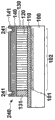
Figure 1A and 1B are the diagrams of example fabrication method that the radiation detecting apparatus of some embodiments of the present invention is shown.
Fig. 2 A to 2F is the diagram that the modification of the embodiment in Figure 1A and 1B is shown.
Fig. 3 is the diagram of example fabrication method that the radiation detecting apparatus of some embodiments of the present invention is shown.
Fig. 4 is the diagram of example fabrication method that the radiation detecting apparatus of some embodiments of the present invention is shown.
Embodiment
Embodiments of the invention are described below with reference to accompanying drawings.Through different embodiment, similarly element is given identical Reference numeral, and will omit its redundancy and describe.And embodiment can suitably be revised or be combined.Embodiments of the invention relate to the manufacture method of radiation detecting apparatus and this radiation detecting apparatus, and this radiation detecting apparatus comprises that a plurality of pixels for detection of light convert with the pel array of arranged in arrays and by the radioactive ray of incident that have can be by the scintillator layers of the light of the wavelength of pixel detection to.Embodiments of the invention relate in particular to the short radiation detecting apparatus of distance from pel array to radiation detecting apparatus edge on its a part of limit, as the radiation detecting apparatus for breast photography (mammography).Below, to this short limit of the distance at radiation detecting apparatus edge, will be called as narrow architrave limit thereon.
With reference to Figure 1A and 1B, describe according to the manufacture method of the radiation detecting apparatus of the first embodiment of the present invention.First, as shown in Figure 1A, preparation has the structure of sensor base plate 100, is formed with cover layer 110, scintillator layers 120, sealant 130 and 131 and protective layer 140 and 141 on described sensor base plate 100.In Figure 1A, figure below is the plane graph of this structure, and top right plot is the right side view of this structure, and the picture left above is the cross-sectional view of this structure of obtaining of A-A along the line.For illustrative purposes, plane graph shows sensor base plate 100, scintillator layers 120 and sealant 130 and 131, and has omitted other assembly.
On sensor base plate 100, formed the pel array 102 having with a plurality of pixels 101 of arranged in arrays.Pixel 101 will be converted to electric charge from the light of radioactive ray conversion by scintillator layers 120.Can (for example pass through known method) by any method and form pel array 102, and therefore will omit its detailed description.For example, each pixel 101 can consist of switch element and photo-electric conversion element, and this switch element is made by amorphous silicon or polysilicon.And ccd sensor or cmos sensor can consist of pel array 102.And sensor base plate 100 can comprise for protecting the sensor protection layer of pel array 102 on the surface at sensor base plate 100.
In the present embodiment, in the outside of the pel array 102 of sensor base plate 100, the one side along pel array 102 forms scribe line (scribe line) 103.In processing described later, use scribe line 103 to serve as a mark and cut sensor base plate 100.Scribe line 103 is the grooves that form for 2mm for example or less position in the distance from pel array 102.
Subsequently, use the technology such as slit coating, spin coating or silk screen printing, on sensor base plate 100, form by the cover layer 110 of making such as the resin of polyimides (PI).By cover layer 110, the adhesiveness between scintillator layers 120 and sensor base plate 100 improves, thereby causes the manufacture output of increase.In another embodiment of the present invention, the unnecessary necessary cover layer 110 that forms, scintillator layers 120 can be formed directly on sensor base plate 100.
Subsequently, on cover layer 110, form sealant 130 and 131 to cover the periphery of pel array 102.Can first form sealant 130(first) or sealant 131(second portion).In the present embodiment, form thereon on the limit of scribe line 103 and form sealant 130, and sealant 131 is formed on other limit.Sealant 130 is formed on scribe line 103.Sealant 130 and 131 can be made by epoxy resin, silicones, acrylic resin, acrylic acid-organic siliconresin (acrylic-silicone resin), ultraviolet ray (UV) cured resin or phenolic resins etc.Although sealant 130 and sealant 131 are made by different materials in the present embodiment, they can be made by identical material in another embodiment.Sealant 130 and the 131 moisture-resistant adhesion layers as scintillator layers 120.
Because sealant 130 in processing described later is cut together with sensor base plate 100, so it can be made by the material that is applicable to cutting.For example, at sealant 130, can be cut the carbon dioxide laser (CO of aluminum oxide (alunite), aluminium, polytetrafluoroethylene, stainless steel, acrylic resin, glass and quartz glass etc.
2laser) in the situation of cutting, sealant 130 can be made by acrylic resin.In the material of enumerating in the above, because the absorbing wavelength of acrylic resin is consistent with the emission wavelength of laser beam machine (10.6 μ m), so acrylic resin is suitable for cutting.And if acrylic resin is cut, the moisture-proof characteristic of acrylic resin is because the heat that carbon dioxide laser produces improves.Due to its narrowed width when sealant 130 is cut, so sealant 130 can be made by black resin, to improve it, stop from outside light and stop the function from the scattering of light of scintillator layers 120.For example, can be by the acrylic resin that becomes the material of sealant 130 is mixed to obtain black resin with carbon black etc.
In processing described later, sealant 131 is not cut, thereby needn't consider whether it is suitable for cutting.For this reason, the material that sealant 131 can be better than the moisture-proof characteristic of sealant 130 by moisture-proof characteristic is made.For example, the epoxy resin that sealant 131 can be better than the moisture-proof characteristic of acrylic resin by moisture-proof characteristic is made.
Usually, using different materials to manufacture in the situation of sealant 130 and sealant 131, can selection material so that sealant 130 is more suitable in cutting than sealant 131, and the moisture-proof characteristic of sealant 131 is better than the moisture-proof characteristic of sealant 130.For example, the such combination except above-mentioned example example can be the sealant 130 of being made by silicones and the sealant 131 of being made by epoxy resin.
Subsequently, use mask to cover except the region by outside sealant 130 and 131 regions (that is, pel array 102 parts) that surround, and by formation scintillator layers 120 such as vacuum moulding machines.For example, scintillator layers 120 is formed by the aggregate (set) of the crystal with column structure by growths such as vapour deposition cesium iodide (CsI) or sodium iodides (NaI).As the dopant for vapour deposition (activator), thallium (Tl) or sodium (Na) etc. can be used.For cover sealant 130 and 131 above and the material of the mask of the part outside sealant 130 and 131 of cover layer 110 can be adhesive tape, metal mask, glass mask, ceramic mask or sheet rubber mask etc.In using the situation of adhesive tape, can use the Kapton Tape with good heat resistance, and in using the situation of sheet rubber, can use fluorubber.Scintillator layers 120 can be grown, so that its height distance of cover layer 110 (that is, from) equals the height distance of cover layer 110 (that is, from) of sealant 130 and 131.Height by scintillator layers 120 is set to identical with the height of sealant 130 and 131, by protective layer 140 and 141 sealing properties that realize, is improved.In another embodiment of the present invention, scintillator layers 120 can have the height different from the height of sealant 130 and 131.
Subsequently, protective layer 140 and 141 be engaged to scintillator layers 120 above and sealant 130 and 131 above.Now, by protective layer 140 being joined to the sheet of protective layer 141 acquisitions, can be engaged to scintillator layers 120 and sealant 130 and 131.Instead, protective layer 140 can be engaged to scintillator layers 120 and sealant 130 and 131, and then protective layer 141 can further be joined to there.Protective layer 140 is used as moisture-resistant protective layer and the adhesion layer of scintillator layers 120, and such as being made by thermoplastic resin (HM), PETG (PET) or polyimides (PI) etc.In these materials, the thermoplastic resin with good moisture-proof characteristic can be used to form protective layer 140.Thermoplastic resin refer to do not comprise water or solvent, room temperature is adhered resin solid-state and that made by the thermoplastic of 100% fixedness.Thermoplastic resin melts when resin temperature rises, and solidifies when resin temperature declines.And thermoplastic resin adheres to other organic material and inorganic material when in heating and melting state, and there is no adhesiveness when room temperature in solid-state.And, because thermoplastic resin does not comprise polar solvent, solvent or water, for example, so it does not make scintillator layers (, the scintillator layers with columnar crystal structure of being made by the alkali halide) fusing of hygroscopy, even also like this when contacting with scintillator layers.Protective layer 141 is as moisture-resistant protective layer and the reflector of scintillator layers 120, and such as being the metal level of being made by aluminium (AL) etc., or the metal/resin stepped construction of being made by Al/PET or Al/PI etc.Although formed in the present embodiment two protective layers 140 and 141, protective layer can be individual layer.Usually, protective layer can be made and can be had the structure of any type by the material of any type, if it can cover scintillator layers 120 above and there is moisture-proof characteristic.
Subsequently, as shown in Figure 1B, with scribe line 103, serve as a mark to cut the structure shown in Figure 1A, to manufacture radiation detecting apparatus 150.In Figure 1B, figure below is the plane graph of radiation detecting apparatus 150, and top right plot is the right side view of radiation detecting apparatus 150, and the picture left above is the cross-sectional view of the radiation detecting apparatus 150 that obtains of B-B along the line.For illustrative purposes, plane graph shows sensor base plate 100, scintillator layers 120 and sealant 130 and 131, and has omitted other assembly.Because cover layer 110, sealant 130 and protective layer 140 and 141 are formed on scribe line 103, thus cover layer 110, sealant 130 and protective layer 140 with 141 by use scribe line 103 serve as a mark cutting sensor base plate 100 also by together with cut.Can carry out cutting by means of diamond saw, stripping and slicing (dicing) or carbon dioxide laser etc.Therefore, the cutting surfaces of the cutting surfaces of sensor base plate 100, cover layer 110 is, the cutting surfaces of the cutting surfaces of sealant 130 and protective layer 140 and 141 is in the same plane.
In the radiation detecting apparatus 150 obtaining by above-mentioned manufacture method; sealant and protective layer are not formed on the side of sensor base plate 100 on one side of radiation detecting apparatus 150, and the distance that therefore shortens the edge from pel array 102 to radiation detecting apparatus 150 is possible.In the present embodiment, the edge of radiation detecting apparatus 150 is consistent with scribe line 103 on this narrow architrave limit.And, due to sensor base plate 100, cover layer 110, sealant 130, the cutting of protective layer 140He141Bei collective, so manufacture process is simplified.In addition, due to use have moisture- proof characteristic sealant 130 and 131 and protective layer 140 and 141 cover scintillator layers 120, so it does not weaken the moisture-proof characteristic of radiation detecting apparatus 150.And; because sealant or protective layer are not formed on the back side of sensor base plate 100; so even radiation detecting apparatus 150 is radiation detecting apparatus of so-called rear surface irradiation type (back-side illumination type); protective layer does not cause artifact (artifact) yet, the radiation detecting apparatus of the so-called rear surface irradiation type radiation detecting apparatus that to be radioactive ray enter from the back side of sensor base plate 100.
Although be on one side only narrow architrave limit in four limits of radiation detecting apparatus 150 in the above-described embodiments, in another embodiment, polygonly can be formed narrow architrave limit by applying said method to it.For example, two relative edges of radiation detecting apparatus can be narrow architrave limit, or two adjacent sides can be narrow architrave limit.Alternately, three limits of radiation detecting apparatus can be narrow architrave limit, or four all limits can be narrow architrave limit.In this case, sealant 130 can be disposed on narrow architrave limit, and sealant 131 can be disposed on other limit.
And, in the above-described embodiments, use sealant 130 and 131 to cover all four sides of scintillator layers 120.Yet, in another embodiment, can comprise narrow architrave limit one side or more polygon on use sealant to cover the side of scintillator layers 120, and can use protective layer 140 and 141 or other moisture-resistant sheet cover other side of scintillator layers 120.
Next, will use Fig. 2 A to 2F to describe the different modification of the manufacture method of above-mentioned the first embodiment.These modification can be by appropriately combined.Fig. 2 A is the plane graph of the radiation detecting apparatus 210 of the first modification.Except radiation detecting apparatus 210 comprises electric assembly 211, radiation detecting apparatus 210 is similar with radiation detecting apparatus 150.Electricity assembly 211 is for the signal being obtained by pixel 101 is outputed to outside assembly, and for example the flexible cable with IC, consists of.Electricity assembly 211 is disposed on the limit except narrow architrave limit.Although it is disposed on the limit relative with narrow architrave limit in the example of Fig. 2 A, it can be disposed on the limit adjacent with narrow architrave limit.And it can be disposed on the only one side or both sides in three limits except narrow architrave limit, or on all this three limits.Electricity assembly 211 can scintillator layers 120, sealant 130 and 131 and protective layer 140 and 141 be formed on sensor base plate 100 before forming, or can after their form, be formed on sensor base plate 100.And electric assembly 211 can form before sensor base plate 100 grades are cut, or can after they are cut, form.
Fig. 2 B is the cross-sectional view of the radiation detecting apparatus 220 of the second modification.Except sensor base plate 100 comprises convergent (tapered) part 221, radiation detecting apparatus 220 is similar with radiation detecting apparatus 150.The part that comprises the limit being formed with the back side (face relative with the face that is formed with scintillator layers 120 on it) by cutting surfaces among the limit of sensor base plate 100 of the radiation detecting apparatus 150 shown in Figure 1B by removal, forms tapered portion 221.Consider the easiness of manufacture, the angle of tapered portion 221 can be 45 degree.The chamfer dimesion of tapered portion 221 (chamfer dimension) can be less than or equal to C1.If sensor base plate 100 is made by glass, chamfer dimesion can be greater than or equal to C0.3, for example C0.5 so.
The result as sensor base plate 100 with tapered portion 221, cracks etc. are removed from sensor base plate 100, and the mechanical strength of sensor base plate 100 increases, and the durability of radiation detecting apparatus 220 improves.And, at radiation detecting apparatus 220, be in the situation of radiation detecting apparatus of rear surface irradiation type, as sensor base plate 100, there is the result of tapered portion 221, the artifact that approaches cutting surfaces can be reduced.Tapered portion 221 can only form on narrow architrave limit as shown in Figure 2 B, or tapered portion 221 can form in addition on other limit of sensor base plate 100.
Fig. 2 C is the cross-sectional view of the radiation detecting apparatus 230 of the 3rd modification.Except the sensor base plate 100 of radiation detecting apparatus 230 has polishing part (the polished portion) 231 that replaces tapered portion 221, radiation detecting apparatus 230 is similar with radiation detecting apparatus 220.By polishing, also grind the part on the limit being formed with the back side (face relative with the face that is formed with scintillator layers 120 on it) by cutting surfaces among the limit of the sensor base plate 100 that comprises the radiation detecting apparatus 150 shown in Figure 1B, form each polishing part 231.
Fig. 2 D is the cross-sectional view of the radiation detecting apparatus 240 of the 4th modification.Except radiation detecting apparatus 240 has heat sealing part 241 in protective layer 140 and 141, radiation detecting apparatus 240 is similar with radiation detecting apparatus 150.Heat sealing part 241 is as the result from heat seal protective layer 140 above and 141 and the part thinner than the other parts of protective layer 140 and 141.Heat sealing part 241 can be formed on sealant 130 and 131, or can be formed on sealant 130 and 131 and scintillator layers 120 on.As the result that has formed heat sealing part 241, the moisture-proof characteristic of scintillator layers 120 improves.Heat sealing part 241 can form before the cutting process of the first embodiment, or can after cutting process, form.If heat sealing part 241 formed before cutting process, can improve so the moisture-proof characteristic of scintillator layers 120 during cutting process.In the part of the sealant 130 that heat sealing part 241 can only attenuate due to cutting at its width of covering, form, or can there is the closed line shape around scintillator layers 120.
Fig. 2 E is the cross-sectional view of the radiation detecting apparatus 250 of the 5th modification.Except radiation detecting apparatus 250 has the heat sealing part 251 that replaces heat sealing part 241, radiation detecting apparatus 250 is similar with radiation detecting apparatus 240.Heat sealing part 251 can form similarly with heat sealing part 241, but forms in the capped position of the cutting surfaces of sealant 130.For example, before cutting process, by form heat sealing part 251 in the capped position of scribe line 103 on protective layer 140 and 141, form one of such heat sealing part 251.The heat sealing part 251 forming is like this cut together with sensor base plate 100 grades in cutting process.As a result, the cutting surfaces of heat sealing part 251 is also positioned in the plane identical with the cutting surfaces of sensor base plate 100 grades.
Fig. 2 F illustrates in the radiation detecting apparatus 260 of the 6th modification the cross-sectional view in the amplification of sealant 130 part around.In the first embodiment, scintillator layers 120 forms after sealant 130 and 131 forms, yet on the contrary, in the 6th modification, sealant 130 and 131 forms after scintillator layers 120 forms.In the 6th modification, can use the aggregate of column crystal 121 to form scintillator layers 120, and sealant 130 and 131 can be made by the resin before solidifying with mobile performance.In this case, a part that is used to form the resin of sealant 130 enters between the post of column crystal 121.As a result, further improve the moisture-proof characteristic of scintillator layers 120.
The manufacture method of radiation detecting apparatus is according to a second embodiment of the present invention described with reference to Fig. 3.To be given identical Reference numeral with assembly like the component class of the first embodiment, and will omit its redundancy and describe.And the modification of the first embodiment can be applied to the second embodiment similarly.First, preparation has the structure of sensor base plate 100, is formed with cover layer 110, scintillator layers 120a and 120b, sealant 330,331a and 331b, and protective layer 140 and 141 on sensor base plate 100.In Fig. 3, figure below is the plane graph of this structure, and top right plot is the right side view of this structure, and the picture left above is the cross-sectional view of this structure of obtaining of C-C along the line.For illustrative purposes, plane graph shows sensor base plate 100, scintillator layers 120a and 120b, and sealant 330,331a and 331b, and omitted other assembly.
On sensor base plate 100, form two pel arrays, i.e. pel array 102a(the first pel array) and pel array 102b(the second pel array), in each of two pel arrays with a plurality of pixels 101 of arranged in arrays.Pel array 102a and 102b can have with the first embodiment in the configuration of the pel array 102 described similarly configure, and will omit its redundancy and describe.Pel array 102a and pel array 102b are adjacent one another are, and are formed so that interval is therebetween for example 4mm or less.Pel array 102a while facing pel array 102b's.In the present embodiment, scribe line 303 is formed between pel array 102a and pel array 102b.
Subsequently, as in the first embodiment, form cover layer 110, and on cover layer 110, form sealant 330,331a and 331b.Sealant 330 can be made by the material of the materials similar of the sealant 130 with the first embodiment, and sealant 331a and 331b can be made by the material of the materials similar of the sealant 131 with the first embodiment.Sealant 330 is formed on the capped position, region between pel array 102a and pel array 102b.Sealant 331a is in surrounding's formation on residue three limits of pel array 102a.Sealant 331b is in surrounding's formation on residue three limits of pel array 102b.
Subsequently, similar with the scintillator layers 120 of the first embodiment, form to cover the scintillator layers 120a(primary scintillator layer of pel array 102a) and the scintillator layers 120b(secondary fluor layer of covering pel array 102b).Can in processing, same vapour deposition form scintillator layers 120a and scintillator layers 120b.Use sealant 330 to cover a side (that is, in the face of the side of scintillator layers 120b) of the scintillator layers 120a forming like this, and use sealant 331a to cover the residue side of scintillator layers 120a.And, use sealant 330 to cover a side (that is, in the face of the side of scintillator layers 120a) of the scintillator layers 120b forming like this, and use sealant 331b to cover the residue side of scintillator layers 120b.
Subsequently, as in the first embodiment, form protective layer 140 and 141.Afterwards, with scribe line 303, serve as a mark to cut sensor base plate 100 as in the first embodiment, thus cover layer 110, sealant 330 and protective layer 140 with 141 also by together with cut.In the present embodiment, by carrying out single vapour deposition, process and single cutting process, can once form each at two radiation detecting apparatus 150 shown in Figure 1B.As a result, can reduce quantity and the manufacturing cost of processing.
To use Fig. 4 to describe the manufacture method of the radiation detecting apparatus of a third embodiment in accordance with the invention.To be given identical Reference numeral with assembly like the component class of the first embodiment, and will omit its redundancy and describe.And the modification of the first embodiment can be applied to the 3rd embodiment similarly.First, preparation has the structure of sensor base plate 100, forms cover layer 110, scintillator layers 120a and 120b, sealant 430,431a and 431b, and protective layer 140 and 141 on sensor base plate 100.In Fig. 4, figure below is the plane graph of this structure, and top right plot is the right side view of this structure, and the picture left above is the cross-sectional view of this structure of obtaining of D-D along the line.For illustrative purposes, plane graph shows sensor base plate 100, scintillator layers 120a and 120b, and sealant 430,431a and 431b, and omitted other assembly.
On sensor base plate 100, form two pel arrays, i.e. pel array 102a(the first pel array) and pel array 102b(the second pel array), in each of two pel arrays with a plurality of pixels 101 of arranged in arrays.Pel array 102a and 102b can have with the first embodiment in the configuration of the pel array 102 described similarly configure, and will omit its redundancy and describe.Pel array 102a and pel array 102b are adjacent one another are, and are formed so that interval is therebetween for example 4mm or less.Pel array 102a while facing pel array 102b's.In the present embodiment, along pel array 102a form scribe line 403a with it in the face of one of adjacent limit, the limit of pel array 102b, and form scribe line 403b between pel array 102a and pel array 102b.Scribe line 403a is also along the limit of pel array 102b.
Subsequently, as in the first embodiment, form cover layer 110, and on cover layer 110, form sealant 430,431a and 431b.Sealant 430 can be made by the material of the materials similar of the sealant 130 with the first embodiment, and sealant 431a and 431b can be made by the material of the materials similar of the sealant 131 with the first embodiment.Sealant 430 is formed on the capped position, region between pel array 102a and pel array 102b, one side and in pel array 102a and 102b each adjacent with this region around.Sealant 431a is in surrounding's formation on the residue both sides of pel array 102a.Sealant 431b is in surrounding's formation on the residue both sides of pel array 102b.
Subsequently, in the similar mode of scintillator layers 120 with the first embodiment, form the scintillator layers 120a(primary scintillator layer that covers pel array 102a) and the scintillator layers 120b(secondary fluor layer of covering pel array 102b).Can in processing, same vapour deposition form scintillator layers 120a and scintillator layers 120b.Use sealant 430 to cover two adjacent side (that is, in the face of the side of scintillator layers 120b and the side being adjacent) of the scintillator layers 120a forming like this, and use sealant 431a to cover the residue side of scintillator layers 120a.And, use sealant 430 to cover two sides (in the face of the side of scintillator layers 120a and the side being adjacent) of the scintillator layers 120b forming like this, and use sealant 431b to cover the residue side of scintillator layers 120b.
Subsequently, as in the first embodiment, form protective layer 140 and 141.Afterwards, with scribe line 403a, serve as a mark to cut sensor base plate 100, then with scribe line 403b, serve as a mark to cut sensor base plate 100, thereby, cover layer 110, sealant 330 and protective layer 140 with 141 also by together with cut.The cutting process that cutting process separately can be similar to the first embodiment is performed.In the present embodiment, by carrying out single vapour deposition, process and two cutting process, can once form two radiation detecting apparatus with two narrow architrave limits.As a result, can reduce quantity and the manufacturing cost of processing.
Here, in the face of arranging on it on the limit on limit of scribe line 403a, prepare scribe line 403c crossing over (across) scintillator layers 120b.On the one hand, can serve as a mark to cut sensor base plate 100 with scribe line 403a, and on the other hand, can serve as a mark to cut sensor base plate 100 with scribe line 403c.Thus, not only can reduce quantity and the manufacturing cost of processing, and can manufacture the same radiation detecting apparatus with two narrow architrave limits.In addition, can manufacture the same radiation detecting apparatus with three narrow architrave limits by cutting scribe line 403a, 403b and 403c.
Although described the present invention with reference to exemplary embodiment, it being understood that the present invention is not limited to disclosed exemplary embodiment.The scope of following claim will be endowed the widest explanation, so that the 26S Proteasome Structure and Function that comprises all such modifications and be equal to.
Claims (11)
1. a method of manufacturing radiation detecting apparatus, comprising:
Be formed with thereon on the sensor base plate of pel array, form cover the scintillator layers of pel array, cover scintillator layers side sealant and cover scintillator layers above and the protective layer above of sealant; And
Along limit cutting sensor base plate, sealant and the protective layer of pel array, so that the cutting surfaces of the cutting surfaces of sensor base plate, sealant and the cutting surfaces of protective layer are arranged at grade.
2. according to the method for claim 1,
Wherein, other the second portion of one or more sides that sealant comprises the first of one or more sides that cover scintillator layers and covers scintillator layers, and
During cutting, the first of sealant is cut.
3. according to the method for claim 2,
Wherein, the material of moisture-proof characteristic that the second portion of sealant is better than the first of sealant by moisture-proof characteristic is made.
4. according to the method for claim 1, further comprise:
Towards sealant, protective layer is carried out to heat seal, to form the heat sealing part in protective layer.
5. according to the method for claim 4,
Wherein, during cutting, protective layer is cut in heat sealing part.
6. according to the method for claim 1,
Wherein, described formation comprises along the limit of pel array and on sensor base plate, forms scribe line,
Sealant is formed on scribe line, and
Use scribe line to carry out cutting.
7. according to the method for claim 1,
Wherein, described formation is used resin to form sealant after being included in the aggregate formation scintillator layers of using column crystal, and
The resin that is used to form sealant enters between the post of aggregate of column crystal.
8. according to the method for claim 1, further comprise:
Remove the part at the back side of sensor base plate, so that the thickness of sensor base plate becomes thinner towards the cutting surfaces of sensor base plate.
9. according to the method for claim 1,
Wherein, during described formation, the first pel array adjacent one another are and the second pel array are respectively used as described pel array and are formed on sensor base plate, while and the first pel array face the second pel array,
Scintillator layers comprises the primary scintillator layer that covers the first pel array and the secondary fluor layer that covers the second pel array,
Sealant covers the side of primary scintillator layer and the side of secondary fluor layer,
Protective layer cover primary scintillator layer above, secondary fluor layer above and sealant above, and
During cutting, sensor base plate, sealant and the protective layer position between the first pel array and the second pel array is cut.
10. according to the method for claim 9, further comprise:
Before cutting, along the first pel array with it in the face of the limit of the second pel array adjacent limit cutting sensor base plate, sealant and protective layer.
11. 1 kinds of radiation detecting apparatus, comprising:
The sensor base plate with pel array;
Cover the scintillator layers of pel array;
Cover the sealant of the side of scintillator layers; And
Cover scintillator layers above and sealant above protective layer,
Wherein, at least one side of sensor base plate is positioned in the plane identical with the side of protective layer with the side of sealant.
Applications Claiming Priority (2)
| Application Number | Priority Date | Filing Date | Title |
|---|---|---|---|
| JP2012-150751 | 2012-07-04 | ||
| JP2012150751A JP6071283B2 (en) | 2012-07-04 | 2012-07-04 | Radiation detection apparatus and manufacturing method thereof |
Publications (1)
| Publication Number | Publication Date |
|---|---|
| CN103531600A true CN103531600A (en) | 2014-01-22 |
Family
ID=49877884
Family Applications (1)
| Application Number | Title | Priority Date | Filing Date |
|---|---|---|---|
| CN201310270654.1A Pending CN103531600A (en) | 2012-07-04 | 2013-07-01 | Radiation detection apparatus and method of manufacturing the same |
Country Status (3)
| Country | Link |
|---|---|
| US (1) | US9054012B2 (en) |
| JP (1) | JP6071283B2 (en) |
| CN (1) | CN103531600A (en) |
Cited By (2)
| Publication number | Priority date | Publication date | Assignee | Title |
|---|---|---|---|---|
| CN105989906A (en) * | 2015-03-18 | 2016-10-05 | 佳能株式会社 | Radiation detection apparatus, radiation imaging system, and manufacturing method |
| CN116722023B (en) * | 2023-08-10 | 2023-12-01 | 奕瑞影像科技(太仓)有限公司 | TFT core component suitable for DR flat panel detector and preparation method thereof |
Families Citing this family (15)
| Publication number | Priority date | Publication date | Assignee | Title |
|---|---|---|---|---|
| US9702986B2 (en) * | 2013-05-24 | 2017-07-11 | Teledyne Dalsa B.V. | Moisture protection structure for a device and a fabrication method thereof |
| JP2015021752A (en) | 2013-07-16 | 2015-02-02 | キヤノン株式会社 | Radiation imaging apparatus, manufacturing method thereof and radiation inspection device |
| JP6310216B2 (en) | 2013-09-06 | 2018-04-11 | キヤノン株式会社 | Radiation detection apparatus, manufacturing method thereof, and radiation detection system |
| JP2015096823A (en) | 2013-11-15 | 2015-05-21 | 浜松ホトニクス株式会社 | Radiation detector and radiation detector manufacturing method |
| JP6310703B2 (en) * | 2014-01-21 | 2018-04-11 | 株式会社日立製作所 | Radiation detector and X-ray CT apparatus using the same |
| JP6333034B2 (en) * | 2014-04-11 | 2018-05-30 | キヤノン株式会社 | Manufacturing method of radiation imaging apparatus |
| CA2968415C (en) | 2014-11-21 | 2020-10-27 | Anton Petrus Maria Van Arendonk | Mammography detector with small chest distance |
| JP6512830B2 (en) | 2015-01-09 | 2019-05-15 | キヤノン株式会社 | Radiation imaging apparatus, method of manufacturing the same, and radiation inspection apparatus |
| JP6487263B2 (en) * | 2015-04-20 | 2019-03-20 | 浜松ホトニクス株式会社 | Radiation detector and manufacturing method thereof |
| JP6191728B2 (en) | 2015-08-10 | 2017-09-06 | 大日本印刷株式会社 | Image sensor module |
| US11156727B2 (en) * | 2015-10-02 | 2021-10-26 | Varian Medical Systems, Inc. | High DQE imaging device |
| JP6778118B2 (en) | 2017-01-13 | 2020-10-28 | キヤノン株式会社 | Radiation imaging device and radiation imaging system |
| WO2019012846A1 (en) | 2017-07-10 | 2019-01-17 | キヤノン株式会社 | Radiation imaging device and radiation imaging system |
| JP7030478B2 (en) | 2017-11-09 | 2022-03-07 | キヤノン株式会社 | Shooting table and radiography system |
| JP7067912B2 (en) | 2017-12-13 | 2022-05-16 | キヤノン株式会社 | Radiation imaging device and radiation imaging system |
Citations (4)
| Publication number | Priority date | Publication date | Assignee | Title |
|---|---|---|---|---|
| US5179284A (en) * | 1991-08-21 | 1993-01-12 | General Electric Company | Solid state radiation imager having a reflective and protective coating |
| US6608312B1 (en) * | 1999-09-03 | 2003-08-19 | Canon Kabushiki Kaisha | Information reading apparatus, method of producing same, and radiation imaging system having same |
| US7265371B2 (en) * | 2004-06-10 | 2007-09-04 | Konica Minolta Medical & Graphic, Inc. | Radiation image conversion panel |
| US20080116381A1 (en) * | 2006-11-22 | 2008-05-22 | Masashi Kondo | Scintillator panel, method of manufacturing the same and radiation imaging apparatus |
Family Cites Families (25)
| Publication number | Priority date | Publication date | Assignee | Title |
|---|---|---|---|---|
| JP3405706B2 (en) * | 1997-02-14 | 2003-05-12 | 浜松ホトニクス株式会社 | Radiation detection element |
| US7315027B2 (en) | 2003-10-22 | 2008-01-01 | Canon Kabushiki Kaisha | Radiation detection device, scintillator panel, method of making the same, making apparatus, and radiation image pick-up system |
| JP4563042B2 (en) * | 2004-01-29 | 2010-10-13 | 浜松ホトニクス株式会社 | Radiation image sensor |
| JP2005246193A (en) * | 2004-03-03 | 2005-09-15 | Konica Minolta Holdings Inc | Method for producing composite film, particle for thermal spraying, composite film and radiation image transformation panel using the composite film |
| US7834323B2 (en) * | 2004-05-11 | 2010-11-16 | Hamamatsu Photonics K.K. | Radiation imaging device |
| JP4266898B2 (en) | 2004-08-10 | 2009-05-20 | キヤノン株式会社 | Radiation detection apparatus, manufacturing method thereof, and radiation imaging system |
| US7514686B2 (en) | 2004-08-10 | 2009-04-07 | Canon Kabushiki Kaisha | Radiation detecting apparatus, scintillator panel, their manufacturing method and radiation detecting system |
| JP4208790B2 (en) | 2004-08-10 | 2009-01-14 | キヤノン株式会社 | Manufacturing method of radiation detection apparatus |
| JP4594188B2 (en) | 2004-08-10 | 2010-12-08 | キヤノン株式会社 | Radiation detection apparatus and radiation detection system |
| JP4671449B2 (en) * | 2004-08-10 | 2011-04-20 | キヤノン株式会社 | Radiation detection apparatus and radiation detection system |
| WO2006046434A1 (en) * | 2004-10-28 | 2006-05-04 | Sharp Kabushiki Kaisha | 2-dimensional image detection device and manufacturing method thereof |
| JP2007155662A (en) | 2005-12-08 | 2007-06-21 | Canon Inc | Radiation detector and radiation imaging system using the same |
| JP4921180B2 (en) | 2006-01-25 | 2012-04-25 | キヤノン株式会社 | Radiation detection apparatus and radiation imaging system |
| JP5089195B2 (en) | 2006-03-02 | 2012-12-05 | キヤノン株式会社 | Radiation detection apparatus, scintillator panel, radiation detection system, and method for manufacturing radiation detection apparatus |
| JP2008008899A (en) | 2006-06-02 | 2008-01-17 | Fujifilm Corp | Radiographic image detector |
| US7820976B2 (en) | 2006-06-02 | 2010-10-26 | Fujifilm Corporation | Radiation image detector |
| US20080210871A1 (en) | 2006-06-02 | 2008-09-04 | Fujifilm Corporation | Radiation image detector |
| JP5004848B2 (en) | 2007-04-18 | 2012-08-22 | キヤノン株式会社 | Radiation detection apparatus and radiation detection system |
| JP4834614B2 (en) | 2007-06-12 | 2011-12-14 | キヤノン株式会社 | Radiation detection apparatus and radiation imaging system |
| JP2010014581A (en) * | 2008-07-04 | 2010-01-21 | Fujifilm Corp | Manufacturing method for radiographic image conversion panel |
| US8973245B2 (en) * | 2010-04-07 | 2015-03-10 | Konica Minolta Medical & Graphic, Inc. | Method of manufacturing flat panel detector |
| JP5607426B2 (en) | 2010-05-28 | 2014-10-15 | キヤノン株式会社 | Radiation detection apparatus and radiation imaging system |
| JP5562134B2 (en) | 2010-06-17 | 2014-07-30 | キヤノン株式会社 | Radiation detection apparatus, manufacturing method thereof, and radiation imaging system |
| JP5473835B2 (en) * | 2010-08-31 | 2014-04-16 | 富士フイルム株式会社 | Radiation detector, radiation imaging apparatus, and method of manufacturing radiation detector |
| JP2013029384A (en) | 2011-07-27 | 2013-02-07 | Canon Inc | Radiation detection device, manufacturing method thereof, and radiation detection system |
-
2012
- 2012-07-04 JP JP2012150751A patent/JP6071283B2/en not_active Expired - Fee Related
-
2013
- 2013-06-26 US US13/927,844 patent/US9054012B2/en not_active Expired - Fee Related
- 2013-07-01 CN CN201310270654.1A patent/CN103531600A/en active Pending
Patent Citations (4)
| Publication number | Priority date | Publication date | Assignee | Title |
|---|---|---|---|---|
| US5179284A (en) * | 1991-08-21 | 1993-01-12 | General Electric Company | Solid state radiation imager having a reflective and protective coating |
| US6608312B1 (en) * | 1999-09-03 | 2003-08-19 | Canon Kabushiki Kaisha | Information reading apparatus, method of producing same, and radiation imaging system having same |
| US7265371B2 (en) * | 2004-06-10 | 2007-09-04 | Konica Minolta Medical & Graphic, Inc. | Radiation image conversion panel |
| US20080116381A1 (en) * | 2006-11-22 | 2008-05-22 | Masashi Kondo | Scintillator panel, method of manufacturing the same and radiation imaging apparatus |
Cited By (4)
| Publication number | Priority date | Publication date | Assignee | Title |
|---|---|---|---|---|
| CN105989906A (en) * | 2015-03-18 | 2016-10-05 | 佳能株式会社 | Radiation detection apparatus, radiation imaging system, and manufacturing method |
| CN105989906B (en) * | 2015-03-18 | 2017-12-22 | 佳能株式会社 | Radiation detecting apparatus, radiation imaging system and manufacture method |
| US9971043B2 (en) | 2015-03-18 | 2018-05-15 | Canon Kabushiki Kaisha | Radiation detection apparatus, radiation imaging system, and manufacturing method |
| CN116722023B (en) * | 2023-08-10 | 2023-12-01 | 奕瑞影像科技(太仓)有限公司 | TFT core component suitable for DR flat panel detector and preparation method thereof |
Also Published As
| Publication number | Publication date |
|---|---|
| US20140008749A1 (en) | 2014-01-09 |
| US9054012B2 (en) | 2015-06-09 |
| JP6071283B2 (en) | 2017-02-01 |
| JP2014013193A (en) | 2014-01-23 |
Similar Documents
| Publication | Publication Date | Title |
|---|---|---|
| CN103531600A (en) | Radiation detection apparatus and method of manufacturing the same | |
| KR100514547B1 (en) | Radiation Detector and its Manufacturing Method | |
| US11506799B2 (en) | Radiation detector, and method for producing radiation detector | |
| JP6000680B2 (en) | Radiation detection apparatus, manufacturing method thereof, and imaging system | |
| TW201238042A (en) | Solid-state imaging apparatus | |
| CN109952647B (en) | Imaging element, manufacturing method, and electronic apparatus | |
| US10379229B2 (en) | Radiation detector and method for producing same | |
| JP2009277884A (en) | Method of manufacturing electronic element module, electronic element module, and electronic information apparatus | |
| US9684083B2 (en) | X-ray detector panel | |
| KR20110113482A (en) | Manufacturing method of x-ray image sensor by direct deposition | |
| JP2009086092A (en) | Method of manufacturing optical component and method of manufacturing photographing device | |
| US9513383B1 (en) | Scintillator sealing with foil | |
| JP6535769B2 (en) | Method of manufacturing radiation detector | |
| JP2019164163A (en) | Radiation detector | |
| JP7333244B2 (en) | RADIATION DETECTOR AND METHOD FOR MANUFACTURING RADIATION DETECTOR | |
| US11953631B2 (en) | Scintillator panel, and radiation detector | |
| TW201732838A (en) | Method for manufacturing radiation detection device | |
| CN111149176B (en) | Scintillator panel and radiation detector | |
| JP4501238B2 (en) | Multi-slice radiation detector | |
| CN116724252A (en) | Radiation detector and method for manufacturing radiation detector | |
| TW202142893A (en) | Radiation detector and method for manufacturing radiation detector | |
| KR101263825B1 (en) | Appratus for x-ray image detecting | |
| JP2004266210A (en) | Method for manufacturing radiation imaging device |
Legal Events
| Date | Code | Title | Description |
|---|---|---|---|
| C06 | Publication | ||
| PB01 | Publication | ||
| C10 | Entry into substantive examination | ||
| SE01 | Entry into force of request for substantive examination | ||
| AD01 | Patent right deemed abandoned | ||
| AD01 | Patent right deemed abandoned |
Effective date of abandoning: 20170111 |