JP6333034B2 - Manufacturing method of radiation imaging apparatus - Google Patents
Manufacturing method of radiation imaging apparatus Download PDFInfo
- Publication number
- JP6333034B2 JP6333034B2 JP2014082310A JP2014082310A JP6333034B2 JP 6333034 B2 JP6333034 B2 JP 6333034B2 JP 2014082310 A JP2014082310 A JP 2014082310A JP 2014082310 A JP2014082310 A JP 2014082310A JP 6333034 B2 JP6333034 B2 JP 6333034B2
- Authority
- JP
- Japan
- Prior art keywords
- substrate
- sensor
- scintillator
- manufacturing
- scintillator layer
- Prior art date
- Legal status (The legal status is an assumption and is not a legal conclusion. Google has not performed a legal analysis and makes no representation as to the accuracy of the status listed.)
- Active
Links
Images


Description
本発明は、放射線撮像装置の製造方法に関する。 The present invention relates to the production how the radiation imaging equipment.
従来、狭額縁の放射線撮像装置が、特許文献1、2で提案されている。特許文献1では、大面積撮影用に複数個を並べて用いた際に、つなぎ目付近における解像度低下やシンチレータの剥離を予防し得る構成の放射線撮像装置が開示されている。特許文献2では、マンモグラフィーにおける画質の向上に有利な技術を提供する方法が開示されている。
Conventionally, a radiation imaging apparatus having a narrow frame has been proposed in
特許文献1では、センサパネル上にシンチレータを形成するときに、センサパネルは、その2辺に沿って設けられている電極パッド部分を蒸着用の基板ホルダーの突出部によって支持することにより収容部内に収容されて支持される。一方、センサパネルの受光部に近接している側の蒸着用の基板ホルダーの受光部側には切り欠き部が形成され、センサパネルの側壁の頂部が蒸着室に対して露出されるように配置される。この状態でセンサパネルにシンチレータを形成すると、輝度、MTF(Modulation Transfer Function)等のシンチレータ特性のばらつきが大きくなるという課題がある。シンチレータ特性のばらつきは、蒸着用の基板ホルダーとシンチレータパネルとの材質が異なることによる。蒸着用の基板ホルダーとシンチレータパネルとの材質が異なるとシンチレータ特性のばらつきが大きくなるのは、材質により熱容量やシンチレータの付着率が異なるためである。さらに、シンチレータがヨウ化セシウム(CsI)等の柱状結晶である場合には、センサパネルの端部において柱状シンチレータの垂直性が低下するという課題がある。
In
特許文献2では、センサパネルを保持した保持部を回転させながら蒸着することによってセンサパネルにシンチレータを形成する。しかし、センサパネルと保持部とが異なる材質のため、センサパネルの端部においてシンチレータ特性のばらつきが大きくなるという課題がある。シンチレータ特性のばらつきの原因は、特許文献1と同様に、センサパネルと保持部との材質が異なり、熱容量やシンチレータの付着率が異なることによる。
In
本発明は、端部におけるシンチレータ特性のばらつきを低減した放射線撮像装置を提供することを目的とする。 An object of this invention is to provide the radiation imaging device which reduced the dispersion | variation in the scintillator characteristic in an edge part.
本発明の1つの側面は、センサ基板および該センサ基板の上に光を検出するセンサ部を有するセンサパネルの前記センサ部側の面と、第2の基板の表面と、にシンチレータを蒸着してシンチレータ層を形成する工程と、前記シンチレータ層が形成された前記センサパネルをシンチレータ層が形成された前記第2の基板から分離して放射線撮像装置を取得する工程と、を含み、前記シンチレータ層を形成する工程は、前記センサ基板の側面と前記第2の基板の側面とが接触するかまたは前記シンチレータ層の厚さの2倍以下の間隙をおいて位置するように保持しながら行われることを特徴とする。 One embodiment of the present invention, said sensor portion side surface of the sensor panel having a sensor unit for detecting light on the sensor substrate and the sensor substrate and the surface of the second substrate, the scintillator is deposited Forming a scintillator layer; and separating the sensor panel on which the scintillator layer is formed from the second substrate on which the scintillator layer is formed to obtain a radiation imaging apparatus, the scintillator layer comprising: The forming step is performed while holding the sensor substrate so that the side surface of the sensor substrate and the side surface of the second substrate are in contact with each other or are positioned with a gap of twice or less the thickness of the scintillator layer. Features.
本発明によれば、端部におけるシンチレータ特性のばらつきを低減した放射線撮像装置を提供することができる。 ADVANTAGE OF THE INVENTION According to this invention, the radiation imaging device which reduced the dispersion | variation in the scintillator characteristic in an edge part can be provided.
[第1実施形態]
以下、本発明の第1実施形態の放射線撮像装置の製造方法を図1に基づいて説明する。図1の(a)は、第1実施形態の放射線撮像装置の製造方法を示す断面図である。センサパネル10は、センサ基板(第1の基板)2と、センサ基板2の上に配置された光を検出するセンサ部(画素部)3とを含む。センサ基板2には、ガラス基板等の絶縁性基板、シリコン基板、アルミニウム基板、アモルファスカーボン等のカーボン基板等が使用される。
[First Embodiment]
Hereinafter, the manufacturing method of the radiation imaging device of 1st Embodiment of this invention is demonstrated based on FIG. FIG. 1A is a cross-sectional view illustrating a method for manufacturing the radiation imaging apparatus according to the first embodiment. The
センサパネル10のセンサ部3側の表面にシンチレータ層8を形成するための蒸着用の保持部(ホルダー)1は、錘部材4と協働して、センサパネル10を保持する。ホルダー1は、2枚のセンサパネル10の蒸着面の周縁部を支持する。一方、錘部材4は、センサパネル10の蒸着面側と反対の側の背面における周縁部を押圧する。
A deposition holding unit (holder) 1 for forming the
ホルダー1は、主として金属で形成される。支持部1の材質として、ステンレス、特にSUS304、SUS316が使用される。錘部材4は、センサパネル10の蒸着面と反対の側の背面における周縁部の一部を押圧することによってセンサパネル10自重による撓みを矯正する。錘部材4の材質は、金属、例えばSUS304、SUS316等のステンレスや、フッ素樹脂、ポリイミド樹脂、シリコン樹脂、ポリエーテルエーテルケトン等の樹脂等、撓みを矯正できる部材であれば良く、これらの材質を積層させた構成でも良い。特に、錘部材4として、センサパネル10への蒸着時の熱影響を軽減する樹脂を使用することができる。特に、錘部材4として、ポリイミド樹脂、シリコン樹脂、ポリエーテルエーテルケトン等の耐熱性の樹脂を使用し得る。
The
第1実施形態では、複数のセンサパネル10のセンサ基板2の側面同士が突き当てられて複数のセンサパネル10のセンサ部側の蒸着面が連続して面一となった状態で保持される。このセンサ基板2の側面同士が突き当てられた突き当て部5側の周縁部において、放射線撮像装置は狭額縁部を構成する。
In the first embodiment, the side surfaces of the
ここで突き当て部5とは、以下の2つの条件を満たすものをいう。
(1)複数のセンサ基板2の側面が互いに少なくとも一部で接触している、または、複数のセンサ基板2の側面が互いに間隙をおいて位置していても、側面間の間隙は形成するシンチレータ層8の厚さの2倍以下、好ましくは0.1mm以下である。
(2)複数のセンサパネル10の蒸着面側の表面の段差は、シンチレータ層8の厚さより小さい。
Here, the abutting portion 5 refers to a member that satisfies the following two conditions.
(1) A scintillator that forms gaps between the side surfaces even if the side surfaces of the plurality of
(2) The steps on the surface on the vapor deposition surface side of the plurality of
シンチレータ層8の形成には、真空蒸着法等が使用される。図1の(a)の下部に設置された不図示のるつぼ(容器)内にシンチレータ材料を入れ、真空中で加熱することによって、センサ基板2のセンサ部側の蒸着面にシンチレータ層8が形成される。シンチレータとして、ヨウ化セシウム(CsI)ヨウ化ナトリウム(NaI)等が使用され、ドープ剤(付活剤)として、Tl(タリウム)、Na(ナトリウム)等が使用され、柱状のシンチレータ粒子が形成される。図1の(b)は、第1実施形態の放射線撮像装置の製造方法を示す平面図である。2つのセンサ基板2を突き当て、各センサ基板2の4隅に錘部材4がそれぞれ設置されている。
For the formation of the
シンチレータ層が形成された2つのセンサ基板2を分離して2つの放射線撮像装置を取得する。第1実施形態では、同一の2つのセンサ基板2を突き当てる場合を示した。しかし、突き当てる2枚の基板のうち、1枚がセンサ基板2で、他の1枚がセンサ基板2と同一の熱容量ないしはシンチレータの付着確率をもつ、又は、センサ基板2と同一の材料で形成された第2の基板でも良い。同一の2つのセンサ基板2を突き当てる場合には、2つの超狭額縁の放射線撮像装置が同時に製造できるので製造コストを低減することも可能である。
Two radiation imaging devices are obtained by separating the two
本実施形態では、第1の基板は、センサパネル10の上にシンチレータ層8を直接形成するときに使用されるセンサパネル10を構成するセンサ基板2であった。しかしながら、第1の基板は、シンチレータ層8を形成してシンチレータパネルを取得した後でシンチレータパネルをセンサパネル10に取り付ける場合の、シンチレータが蒸着されてシンチレータパネルを構成する基板(間接基板)であってもよい。間接基板には、シリコン基板、アルミニウム基板、アモルファスカーボン等のカーボン基板等が使用される。
In the present embodiment, the first substrate is the
第1の基板と第2の基板との組合せを以下の表1に示す。 The combinations of the first substrate and the second substrate are shown in Table 1 below.

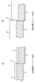
複数のセンサ基板2を突き当てると複数のセンサ基板2の間に段差が発生する場合がある。複数のセンサ基板2の間の段差(表面段差)は小さい方がよい。図5の(b)に示すように、複数のセンサ基板2の蒸着面の段差がシンチレータ層8の厚さを超える場合は、センサ基板2の側面にまでシンチレータが付着し、シンチレータ層8の端部でシンチレータの柱状結晶が傾いて成長する。一方、図5の(a)に示すように、センサ基板2の蒸着面の段差がシンチレータ層8の厚さ以下の場合は、シンチレータ層8の端部でもシンチレータの柱状結晶が垂直に成長する。そのため、シンチレータ層8は、蒸着面に垂直な側壁を有し、均一な厚みとなって、輝度、MTF等のシンチレータ特性のばらつきを低減させることができる。
When a plurality of
[第2実施形態]
以下、第2実施形態の放射線撮像装置の製造方法を図2に基づいて説明する。図2の(a)は、第2実施形態の断面図であり、(b)は、平面図である。第2実施形態においても、第1実施形態と同様に、2枚のセンサ基板2を突き当て部5で突き当てた状態でホルダー1および錘部材4を用いて保持しながらシンチレータ層8を形成する。
[Second Embodiment]
Hereinafter, the manufacturing method of the radiation imaging apparatus of 2nd Embodiment is demonstrated based on FIG. 2A is a cross-sectional view of the second embodiment, and FIG. 2B is a plan view. Also in the second embodiment, as in the first embodiment, the
第2実施形態において第1実施形態と異なるのは、2枚のセンサ基板2の間に2枚のセンサ基板2を接続する接続部材6が設置されているところである。接続部材6としては、センサ基板2と同一の熱容量やシンチレータの付着確率をもつ、センサ基板2と異なる材料が用いられる。また、接続部材6として、センサ基板2と同一の材料が用いられる。接続部材6は、接続部における2枚のセンサ基板2の間の間隙の大きさを一定に規定する役割があり、その間隙の大きさは、0.1mm以下とする。図5を用いて説明したように、2枚のセンサ基板2の間の距離が0.1mmを超えると、シンチレータ特性のばらつきを低減させることが難しくなる。間隙の大きさが0.1mm以下の場合には、互いに接続された接続部においてもヨウ化セシウムの柱状結晶体を垂直に形成でき、シンチレータ特性のばらつきを低減させ得る。
The second embodiment is different from the first embodiment in that a
[第3実施形態]
以下、第3実施形態の放射線撮像装置の製造方法を図3に基づいて説明する。図3は、第3実施形態の断面図である。第3実施形態においても、第1実施形態と同様に、2枚のセンサ基板2を突き当て部5で突き当てた状態でホルダー1および錘部材4を用いて保持しながらシンチレータ層8を形成する。
[Third Embodiment]
Hereinafter, the manufacturing method of the radiation imaging device of 3rd Embodiment is demonstrated based on FIG. FIG. 3 is a cross-sectional view of the third embodiment. Also in the third embodiment, as in the first embodiment, the
第3実施形態では、2枚のセンサ基板2を突き当てた状態で、2枚のセンサ基板2の側面の蒸着面側の一部が互いに接触し、側面の背面側の残部がテーパー形状の空間を形成する。そのテーパー形状に対応した形状の部材7をテーパー形状の空間に配置する。このような構成にすると、突き当て部5における2枚のセンサ基板2の側面同士の接触面積が増えることになる。その結果、突き当て部5でのシンチレータ特性のばらつきをより低減させることができる。
In the third embodiment, in a state where the two
以下、第1〜第3実施形態で使用する複数のセンサパネル10a,10bを取得する方法を図4に基づいて述べる。センサパネル10としては、ガラス基板(保持基板)100上にTFT部およびセンサ部3が形成されたセンサ基板2を用いる場合を示している。大面積のガラス基板100上に複数枚のセンサ基板2が配置されている。本実施形態の場合は、2枚のセンサパネル10a,10bが配置されている。ガラス基板100を切り出して、センサパネル10aとセンサパネル10bを取得する。切断後、切断面を突き当て部5として2枚のセンサパネル10a,10bを蒸着用のホルダー1に設置する。
Hereinafter, a method for obtaining the plurality of
ガラス基板100の切り出す手法としては、スライサー、ダイヤモンドソー、ダイシング、レーザーによる切断等の手法がある。切断部同士を突き当てるため、切断面の凹凸が少なく接触面積が大きくなるレーザーによる切断がより好ましい。量産工程においては、複数のガラス基板100が移動するので、異なるガラス基板100から切り出されたセンサパネル同士を突き当てる場合と、同一のガラス基板100から切り出されたセンサパネル同士を突き当てる場合がある。
As a method for cutting out the
切断面に凹凸が有っても、同一のガラス基板100から切り出されたセンサパネル同士を突き当てる場合の方が、接触面積がより大きく、異なるガラス基板から切り出される場合よりも、シンチレータ特性のばらつきをより低減させ得る。
Even if there are irregularities on the cut surface, the contact area is larger when the sensor panels cut out from the
[他の実施形態]
本実施形態では、2枚のセンサ基板2を保持する方法として、2枚のセンサ基板2を突き当てて保持する場合を図示した。しかし、静電吸着により2枚のセンサ基板2を基台12に保持する方法、または、耐熱性の粘着シート(粘着層)15を介して2枚のセンサ基板2を基台12に保持してもよい。
[Other Embodiments]
In the present embodiment, as a method of holding the two
図6は、静電吸着(静電チャック)により2枚のセンサ基板2を保持した場合を示す。静電チャック9は、基台12の上に誘電層または絶縁層11を設け、基台12とセンサ基板2の間に電圧を印加し、両者の間に発生した力によってセンサ基板2を吸着する。吸着方式の違いによって、クーロン力型とジョンソン・ラベック力型に分類される。誘電体として絶縁材料を使用するのがクーロン力型である。一方、低電圧で強い吸着力を発揮するジョンソン・ラベック力型は、アルミナなどのセラミック製静電チャックに多く使用され、耐熱性と耐プラズマ性の面で優れている。
FIG. 6 shows a case where two
静電チャック9は、機械的な保持具を使用しないためにセンサ基板2の全面を均一に蒸着できる。そのため、センサ基板2を吸着固定用デバイスとして広く普及しており、ヒーターと組み合わせて基板加熱をし、蒸着中の基板温度を制御することが可能である。
Since the electrostatic chuck 9 does not use a mechanical holder, the entire surface of the
電圧印加前,センサ基板2の表面は安定した状態にある。電極パターンに電圧を印加すると、センサ基板2の表面(吸着面)には強い電界が形成され,センサ基板2の表面が分極する。そのため、静電チャック9とセンサ基板2との間に電位差が発生し,お互いを吸引するクーロン力13が誘起されてセンサ基板2を吸着する。吸着した状態にて基台12を回転軸16にて回転させながらシンチレータ(CsI:Tl)を蒸着する。
Before voltage application, the surface of the
リリース(吸着の解除)時には、逆に、静電チャック9への印加電圧を遮断すると、センサ基板2の表面分極を拘束する電極パターンからの電界が消滅する。そのため、センサ基板2の表面分極も瞬時に無くなり、静電チャック9とセンサ基板2表面との間に電位差が無くなり静電吸着力13が消滅する。つまり、印加電圧を遮断するだけでセンサ基板2をリリース(吸着の解除)できる。
On the contrary, when the voltage applied to the electrostatic chuck 9 is cut off at the time of release (release of adsorption), the electric field from the electrode pattern that restrains the surface polarization of the
図7は、耐熱性の粘着シート15により2枚のセンサ基板2を保持した場合の模式図である。基台12の上に粘着シート15を介して、基台12とセンサ基板2を保持する。複数のセンサ基板2を粘着シート15にて保持した状態にて、基台12を回転軸16にて回転させながらシンチレータ(CsI:Tl)を蒸着する。粘着シート15としては、シリコン系、アクリル系、アクリル・シリコン系のシート等が使用される。
FIG. 7 is a schematic view when two
[放射線撮像システム]
上記の各実施形態で製造された放射線撮像装置200を含む放射線撮像システムを、図8を用いて説明する。図8に示すように、X線チューブ(放射線源)210で発生した放射線(X線)211は、患者あるいは被験者220の胸部221を透過し、放射線撮像装置200に入射する。この入射したX線には患者220の体内部の情報が含まれている。X線の入射に対応してシンチレータ層8は発光し、この発光をセンサパネル10のセンサ部(光電変換素子)3が光電変換して、電気的情報を得る。この電気的情報は、デジタルに変換され、信号処理部(イメージプロセッサ)230により画像処理され、表示部(ディスプレイ)240によって観察できる。
[Radiation imaging system]
A radiation imaging system including the radiation imaging apparatus 200 manufactured in each of the above embodiments will be described with reference to FIG. As shown in FIG. 8, the radiation (X-rays) 211 generated by the X-ray tube (radiation source) 210 passes through the
イメージプロセッサ230により画像処理された情報は、電話、LAN、インターネットなどのネットワーク等の伝送処理部250により遠隔地へ転送できる。したがって、イメージプロセッサ230により画像処理された情報は、別の場所のドクタールームなどの表示部(ディスプレイ)241に表示したり、光ディスク等の記録部に保存したりすることができ、遠隔地の医師によって診断可能である。また、イメージプロセッサ230により画像処理された情報は、フィルムプロセッサ260によりフィルム261に記録することもできる。
Information processed by the
本発明の放射線撮像装置200は、医療用の放射線撮像装置や、非破壊検査装置等の放射線を利用した医療用以外の分析、検査用途の装置への応用が可能である。 The radiation imaging apparatus 200 of the present invention can be applied to a medical radiation imaging apparatus or a non-medical analysis or inspection apparatus using radiation, such as a nondestructive inspection apparatus.
1:ホルダー。2:センサ基板。3:センサ部。4:錘部材。5:突き当て部。6:距離調整部材。7:付き当て部材。8:シンチレータ層。10:センサパネル。 1: Holder. 2: Sensor substrate. 3: Sensor part. 4: Weight member. 5: Butting part. 6: Distance adjusting member. 7: Attaching member. 8: Scintillator layer. 10: Sensor panel.
Claims (17)
前記シンチレータ層が形成された前記センサパネルをシンチレータ層が形成された前記第2の基板から分離して放射線撮像装置を取得する工程と、
を含み、
前記シンチレータ層を形成する工程は、前記センサ基板の側面と前記第2の基板の側面とが接触するかまたは前記シンチレータ層の厚さの2倍以下の間隙をおいて位置するように保持しながら行われることを特徴とする放射線撮像装置の製造方法。 Forming a scintillator layer by vapor-depositing a scintillator on a surface of the sensor substrate having a sensor substrate and a sensor panel that detects light on the sensor substrate, and a surface of the second substrate;
Separating the sensor panel on which the scintillator layer is formed from the second substrate on which the scintillator layer is formed to obtain a radiation imaging apparatus;
Including
In the step of forming the scintillator layer, the side surface of the sensor substrate and the side surface of the second substrate are in contact with each other or are held so as to be positioned with a gap less than twice the thickness of the scintillator layer. The manufacturing method of the radiation imaging device characterized by performing.
シンチレータ層が形成された前記第1の基板をシンチレータ層が形成された前記第2の基板から分離してシンチレータパネルを取得する工程と、
センサ基板および該センサ基板の上に光を検出するセンサ部を有するセンサパネルの前記センサ部側に前記シンチレータパネルを取り付けて放射線撮像装置を取得する工程と、
を含み、
前記間隙は、前記シンチレータ層の厚さの2倍以下であることを特徴とする放射線撮像装置の製造方法。 The deposition surface of the first substrate while holding the first substrate and the second substrate so that the side surface of the first substrate and the side surface of the second substrate are in contact with each other or are positioned with a gap therebetween. And forming a scintillator layer by vapor-depositing a scintillator on the vapor deposition surface of the second substrate;
Separating the first substrate on which the scintillator layer is formed from the second substrate on which the scintillator layer is formed, and obtaining a scintillator panel;
Attaching the scintillator panel to the sensor unit side of the sensor panel having a sensor substrate and a sensor unit for detecting light on the sensor substrate to obtain a radiation imaging apparatus;
Including
The method of manufacturing a radiation imaging apparatus, wherein the gap is not more than twice the thickness of the scintillator layer.
Priority Applications (1)
| Application Number | Priority Date | Filing Date | Title |
|---|---|---|---|
| JP2014082310A JP6333034B2 (en) | 2014-04-11 | 2014-04-11 | Manufacturing method of radiation imaging apparatus |
Applications Claiming Priority (1)
| Application Number | Priority Date | Filing Date | Title |
|---|---|---|---|
| JP2014082310A JP6333034B2 (en) | 2014-04-11 | 2014-04-11 | Manufacturing method of radiation imaging apparatus |
Publications (3)
| Publication Number | Publication Date |
|---|---|
| JP2015203606A JP2015203606A (en) | 2015-11-16 |
| JP2015203606A5 JP2015203606A5 (en) | 2017-05-25 |
| JP6333034B2 true JP6333034B2 (en) | 2018-05-30 |
Family
ID=54597130
Family Applications (1)
| Application Number | Title | Priority Date | Filing Date |
|---|---|---|---|
| JP2014082310A Active JP6333034B2 (en) | 2014-04-11 | 2014-04-11 | Manufacturing method of radiation imaging apparatus |
Country Status (1)
| Country | Link |
|---|---|
| JP (1) | JP6333034B2 (en) |
Families Citing this family (1)
| Publication number | Priority date | Publication date | Assignee | Title |
|---|---|---|---|---|
| CN107398844B (en) * | 2017-06-26 | 2019-05-28 | 东软医疗系统股份有限公司 | A kind of detector manufacture fixture and scintillator localization method |
Family Cites Families (5)
| Publication number | Priority date | Publication date | Assignee | Title |
|---|---|---|---|---|
| JP4447752B2 (en) * | 2000-08-03 | 2010-04-07 | 浜松ホトニクス株式会社 | Radiation detector |
| US20050008291A1 (en) * | 2003-07-08 | 2005-01-13 | Baney Dougas M. | Optical wave-guide microstructured environment absorption cell |
| JP5680943B2 (en) * | 2010-11-16 | 2015-03-04 | キヤノン株式会社 | Scintillator, radiation detection device and radiation imaging device |
| JP6071283B2 (en) * | 2012-07-04 | 2017-02-01 | キヤノン株式会社 | Radiation detection apparatus and manufacturing method thereof |
| JP2014048061A (en) * | 2012-08-29 | 2014-03-17 | Canon Inc | Radiation imaging device, manufacturing method of the same, and radiation imaging system |
-
2014
- 2014-04-11 JP JP2014082310A patent/JP6333034B2/en active Active
Also Published As
| Publication number | Publication date |
|---|---|
| JP2015203606A (en) | 2015-11-16 |
Similar Documents
| Publication | Publication Date | Title |
|---|---|---|
| EP1118880B1 (en) | Method of organic film deposition | |
| JP5799953B2 (en) | Flat panel detector | |
| US20090000552A1 (en) | Substrate holder and vacuum film deposition apparatus | |
| JP2012137438A5 (en) | ||
| JP2013002887A (en) | Radiation detection panel and radiographic device | |
| Kuo et al. | Flexible X-ray imaging detector based on direct conversion in amorphous selenium | |
| US9684083B2 (en) | X-ray detector panel | |
| JP5561277B2 (en) | Scintillator panel manufacturing method, scintillator panel, and radiation image detector | |
| JP6333034B2 (en) | Manufacturing method of radiation imaging apparatus | |
| JP4874851B2 (en) | Vacuum deposition system | |
| JP5229320B2 (en) | Scintillator panel and radiation image detection apparatus having the same | |
| US10345455B2 (en) | Radiation detection apparatus, radiation imaging system, and method of manufacturing radiation detection apparatus | |
| JP2010032298A (en) | Scintillator panel | |
| JP2011252732A (en) | Radiation detecting panel and method of manufacturing the same | |
| JP2004325442A (en) | Radiation detector and its manufacturing method | |
| JP2003262678A (en) | Scintillator panel for radiation detector, and manufacturing method thereof | |
| JP2012229999A (en) | Radiation image detecting device and radiographic apparatus | |
| US11947058B2 (en) | Method for producing a solid-state digital detector of incident radiation | |
| US9234271B2 (en) | Radiation imaging apparatus, method of manufacturing the same, and radiation inspection apparatus | |
| JP2015200528A (en) | Radiation imaging apparatus, method of manufacturing the same and radiation imaging system | |
| JP2010060414A (en) | Scintillator plate | |
| JP2007009255A (en) | Film deposition device and film deposition method | |
| JP2017040584A (en) | Manufacturing method for scintillator panel and manufacturing method for radiation imaging apparatus | |
| JP2018080977A (en) | Manufacturing method of radiation detection device, radiation detection device and radiation detection system | |
| JP2006184187A (en) | Radiation detection device, scintillator panel, and radiation detection system |
Legal Events
| Date | Code | Title | Description |
|---|---|---|---|
| A521 | Written amendment |
Free format text: JAPANESE INTERMEDIATE CODE: A523 Effective date: 20170406 |
|
| A621 | Written request for application examination |
Free format text: JAPANESE INTERMEDIATE CODE: A621 Effective date: 20170406 |
|
| A131 | Notification of reasons for refusal |
Free format text: JAPANESE INTERMEDIATE CODE: A131 Effective date: 20180119 |
|
| A977 | Report on retrieval |
Free format text: JAPANESE INTERMEDIATE CODE: A971007 Effective date: 20180117 |
|
| A521 | Written amendment |
Free format text: JAPANESE INTERMEDIATE CODE: A523 Effective date: 20180129 |
|
| TRDD | Decision of grant or rejection written | ||
| A01 | Written decision to grant a patent or to grant a registration (utility model) |
Free format text: JAPANESE INTERMEDIATE CODE: A01 Effective date: 20180326 |
|
| A61 | First payment of annual fees (during grant procedure) |
Free format text: JAPANESE INTERMEDIATE CODE: A61 Effective date: 20180424 |
|
| R151 | Written notification of patent or utility model registration |
Ref document number: 6333034 Country of ref document: JP Free format text: JAPANESE INTERMEDIATE CODE: R151 |