JP4266898B2 - Radiation detection apparatus, manufacturing method thereof, and radiation imaging system - Google Patents
Radiation detection apparatus, manufacturing method thereof, and radiation imaging system Download PDFInfo
- Publication number
- JP4266898B2 JP4266898B2 JP2004233423A JP2004233423A JP4266898B2 JP 4266898 B2 JP4266898 B2 JP 4266898B2 JP 2004233423 A JP2004233423 A JP 2004233423A JP 2004233423 A JP2004233423 A JP 2004233423A JP 4266898 B2 JP4266898 B2 JP 4266898B2
- Authority
- JP
- Japan
- Prior art keywords
- phosphor
- layer
- protective layer
- radiation detection
- photoelectric conversion
- Prior art date
- Legal status (The legal status is an assumption and is not a legal conclusion. Google has not performed a legal analysis and makes no representation as to the accuracy of the status listed.)
- Expired - Fee Related
Links
Images


Classifications
-
- G—PHYSICS
- G01—MEASURING; TESTING
- G01T—MEASUREMENT OF NUCLEAR OR X-RADIATION
- G01T1/00—Measuring X-radiation, gamma radiation, corpuscular radiation, or cosmic radiation
- G01T1/16—Measuring radiation intensity
- G01T1/20—Measuring radiation intensity with scintillation detectors
- G01T1/2006—Measuring radiation intensity with scintillation detectors using a combination of a scintillator and photodetector which measures the means radiation intensity
Description
本発明は、医療診断機器、非破壊検査機器等に用いられるシンチレーターパネル、放射線検出装置および放射線撮像システムに関し、特に、X線撮影等に用いられるシンチレーターパネル、放射線検出装置および放射線撮像システムに関する。なお、本明細書では、X線の他、α線、β線、γ線等の電磁波も、放射線に含まれるものとする。 The present invention relates to a scintillator panel, a radiation detection apparatus, and a radiation imaging system used for medical diagnostic equipment, non-destructive inspection equipment, and the like, and more particularly to a scintillator panel, radiation detection apparatus, and radiation imaging system used for X-ray photography. Note that in this specification, in addition to X-rays, electromagnetic waves such as α rays, β rays, and γ rays are included in radiation.
従来、X線蛍光体層が内部に備えられた蛍光スクリーンと両面塗布剤とを有するX線フィルムシステムが一般的にX線写真撮影に使用されてきた。しかし、最近、X線を可視光に変換する波長変換体としての蛍光体層と光電変換素子を2次元に配列して構成された2次元光検出器とを有するデジタル放射線検出装置の画像特性が良好であること、また、データーがデジタルデーターであるためネットワーク化したコンピュータシステムに取り込むことによってデーターの共有化が図られる利点があることから、デジタル放射線検出装置について盛んに研究開発が行われ、種々の特許出願もされている。 Conventionally, an X-ray film system having a fluorescent screen having an X-ray phosphor layer provided therein and a double-side coating agent has been generally used for X-ray photography. However, recently, the image characteristics of a digital radiation detection apparatus having a phosphor layer as a wavelength converter for converting X-rays into visible light and a two-dimensional photodetector configured by two-dimensionally arranging photoelectric conversion elements have been developed. Since it is good, and because the data is digital data, there is an advantage that data can be shared by importing it into a networked computer system. Therefore, active research and development has been conducted on digital radiation detection devices. Patent applications have also been filed.
これらデジタル放射線検出装置の中でも、高感度で高鮮鋭な装置として、特許文献1に開示されているように、複数のフォトセンサー及びTFT (Thin Film Transistor)等の電気素子が2次元に配置されている光電変換素子部からなる光検出器上(「センサーパネル」とも言う)に、放射線をフォトセンサーで検出可能な光に変換するための蛍光体層を形成してなる放射線検出装置が知られている。
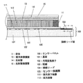
図11は従来の放射線検出装置を示す断面図である。図12は、前述の蛍光体層を複数のフォトセンサー及びTFT等の電気素子が配置されている光電変換素子部からなる2次元のセンサーパネル状に形成した放射線検出装置の断面図である。図12中、101はガラス基板、102はアモルファスシリコンを用いたフォトセンサーであり、TFTとで光電変換部を構成する。また、103は配線、104は接続リード、105は窒化シリコン等よりなるセンサー保護層(第1の保護層)、111は樹脂膜等よりなる蛍光体下地層(第2の保護層)である。112はアルカリハライドよりなる柱状構造結晶を有する蛍光体層、113、115は有機樹脂よりなる蛍光体保護層並びに反射層保護層、114は反射層である。また、116は蛍光体保護層113を形成する前にセンサーパネル上に蛍光体外周に形成される保護樹脂、さらに117は、蛍光体保護層113や反射保護層115の保護膜端部を封止し、外界の水分の進入を防止し、耐久性を向上させるものである。104は、外部の電気回路との接続を行うための接続リードであり、フレキシブル配線板等を異方性導電接着フィルム等を用い電気的に接続される。これら全体で放射線検出装置を構成するものである。
FIG. 11 is a cross-sectional view showing a conventional radiation detection apparatus. FIG. 12 is a cross-sectional view of a radiation detection apparatus in which the above-described phosphor layer is formed in a two-dimensional sensor panel shape including a photoelectric conversion element portion in which a plurality of photosensors and electrical elements such as TFTs are arranged. In FIG. 12, 101 is a glass substrate, 102 is a photosensor using amorphous silicon, and the TFT constitutes a photoelectric conversion unit. Further, 103 is a wiring, 104 is a connection lead, 105 is a sensor protective layer (first protective layer) made of silicon nitride or the like, and 111 is a phosphor base layer (second protective layer) made of a resin film or the like. 112 is a phosphor layer having a columnar structure crystal made of alkali halide, 113 and 115 are a phosphor protective layer and a reflective layer protective layer made of an organic resin, and 114 is a reflective layer. 116 is a protective resin formed on the outer periphery of the phosphor on the sensor panel before forming the phosphor
しかしながら、上記従来例において、センサーパネル上に蛍光体層112を形成する際、蛍光体が付着しては困る接続リード104をマスキングする必要がある。
この場合、蛍光体層を蒸着する装置にセンサーパネルをセットする際のホルダーの形状を、電気接続リード104を覆うようにして近接配置させることで蛍光体の付着を防止することが可能であるが、蛍光体層形成後にホルダーを取外す際に、センサーパネルに帯電した静電気がホルダー等に放電し、電気接続リード104を介してセンサーパネル上に形成されたフォトセンサー102やTFTの特性変化や配線の断線が発生するという問題が生じる恐れがある。また、蛍光体層形成装置にセットする前にポリイミドテープ等を用い接続リードを覆うように貼り付けマスキングすることでも可能であるが、蛍光体層形成後にマスキングテープを剥す際にテープの剥離帯電により、同様にセンサーパネルが帯電し、ハンドリングの接触等により放電を引き起こし同様の不具合が発生するという問題が生じる恐れがある。
また、前述の従来の放射線検出装置の構成やマスキング方法では、マスキングが不完全で電気接続リード104に蛍光体層の付着が発生したり、テープの残渣が残ったりしたため、接続リード104を溶剤等で洗浄処理が必要となり作業の増加を招いている。
However, in the above conventional example, when the
In this case, it is possible to prevent the phosphor from adhering by arranging the holder shape when the sensor panel is set in the apparatus for depositing the phosphor layer so as to cover the
Further, in the above-described configuration and masking method of the conventional radiation detection apparatus, masking is incomplete and phosphor layers adhere to the electrical connection leads 104 or tape residues remain. Therefore, the cleaning process is required, which increases the work.
また、本従来例における蛍光体保護層113、反射層保護層115は、真空蒸着装置を必要とするCVD法(気相成長法)により形成するが、装置が高価で且つ形成時間が非常に長くコスト高を招いている。
Further, the phosphor
本発明の放射線検出装置は、基板上に2次元に配列された複数の光電変換素子からなる受光部と、該受光部の各行又は各列の前記光電変換素子と電気的に接続され、前記受光部の外部に配された複数の電気接続部と、を有するセンサーパネルと、
少なくとも該受光部上に配置された、放射線を前記光電変換素子が感知可能な光に変換する、柱状結晶構造を有する蛍光体層と、
該蛍光体層を被覆し前記センサーパネルと接する、ホットメルト樹脂からなる蛍光体保護部材と、を有する放射線検出装置において、
前記蛍光体保護部材は、前記蛍光体層と前記電気接続部との間の前記センサーパネル上に、前記蛍光体層の側面と接して配置された枠部材と、前記蛍光体層の上面を被覆し、且つ前記枠部材の上面と密着して配置された蛍光体保護層と、を有し、
前記蛍光体保護層は前記枠部材の上面において加熱圧着された加熱圧着部を含み、前記蛍光体保護層の前記加熱圧着部の膜厚は前記加熱圧着部以外の膜厚より薄いことを特徴とする。
本発明の放射線検出装置の製造方法は、基板上に2次元に配列された複数の光電変換素子からなる受光部と、該受光部の各行又は各列の前記光電変換素子と電気的に接続され、前記受光部の外部に配された複数の電気接続部と、を有するセンサーパネルと、
少なくとも該受光部上に配置された、放射線を前記光電変換素子が感知可能な光に変換する蛍光体層と、
を有する放射線検出装置の製造方法であって、
前記受光部と前記電気接続部との間の前記センサーパネル上に枠部材を形成する工程と、
前記枠部材で囲まれた前記センサーパネル上に蒸着により柱状結晶構造を有する前記蛍光体層を配する工程と、
前記蛍光体層の上面を被覆し、且つ前記枠部材の上面と密着するホットメルト樹脂からなる蛍光体保護層を形成する工程と、
前記枠部材の上面において、前記蛍光体保護層を加熱圧着手段で加熱圧着して、前記蛍光体保護層の加熱圧着部の膜厚を前記加熱圧着部以外の膜厚より薄くする工程と、
を有することを特徴とする。
The radiation detection apparatus according to the present invention includes a light receiving unit including a plurality of photoelectric conversion elements arranged two-dimensionally on a substrate, and the photoelectric conversion elements in each row or each column of the light receiving unit, A plurality of electrical connections disposed outside the unit, and a sensor panel,
A phosphor layer having a columnar crystal structure, which is disposed on at least the light receiving portion and converts radiation into light that can be sensed by the photoelectric conversion element;
In a radiation detection apparatus having a phosphor protective member made of a hot melt resin that covers the phosphor layer and is in contact with the sensor panel,
The phosphor protection member covers a frame member disposed in contact with a side surface of the phosphor layer on the sensor panel between the phosphor layer and the electrical connection portion, and covers an upper surface of the phosphor layer. and, and have a, and a phosphor protective layer disposed in close contact with the upper surface of the frame member,
The phosphor protective layer includes a thermocompression bonding part that is thermocompression bonded on the upper surface of the frame member, and the film thickness of the thermocompression bonding part of the phosphor protective layer is thinner than the film thickness other than the thermocompression bonding part. To do.
The method for manufacturing a radiation detection apparatus according to the present invention is electrically connected to a light receiving unit composed of a plurality of photoelectric conversion elements arranged two-dimensionally on a substrate, and the photoelectric conversion elements in each row or each column of the light receiving unit. A sensor panel having a plurality of electrical connections disposed outside the light receiving unit,
A phosphor layer that is disposed on at least the light receiving section and converts radiation into light that can be sensed by the photoelectric conversion element;
A method for manufacturing a radiation detection apparatus comprising:
Forming a frame member on the sensor panel between the light receiving portion and the electrical connection portion;
Disposing the phosphor layer having a columnar crystal structure by vapor deposition on the sensor panel surrounded by the frame member;
Forming a phosphor protective layer made of a hot melt resin that covers the upper surface of the phosphor layer and is in close contact with the upper surface of the frame member;
On the upper surface of the frame member, the phosphor protective layer is thermocompression bonded by thermocompression bonding means, and the film thickness of the thermocompression bonding portion of the phosphor protective layer is made thinner than the film thickness other than the thermocompression bonding portion;
It is characterized by having.
本発明によれば、蛍光体層の形成蒸着装置へのセットの際に、マスキング部分であるホルダー部(マスク部材)を枠部材に密着させるようにセットして非蛍光体層形成領域のマスキングを行い、蛍光体層を堆積することにより、接続リードのマスキングがなされ蛍光体層を形成できるとともにセンサーパネル上の接続リードとホルダーとのクリアランスが保たれ、不用意にホルダーが接続リードに近接するこが防止できる。よって、センサーパネルに帯電した静電気の放電を防止することができ、歩留まりの高く、安定した生産ができる。 According to the present invention, when setting the phosphor layer on the deposition apparatus, the holder part (mask member) which is a masking part is set so as to be in close contact with the frame member to mask the non-phosphor layer forming region. By depositing the phosphor layer, the connection lead is masked to form the phosphor layer, and the clearance between the connection lead on the sensor panel and the holder is maintained, and the holder is inadvertently brought close to the connection lead. Can be prevented. Therefore, it is possible to prevent discharge of static electricity charged in the sensor panel, and high yield and stable production can be achieved.
また、蛍光体層は側壁に形成した水分透過率の低い樹脂からなる枠部材と上面を覆う蛍光体保護層で覆うことにより簡単な構成で耐湿信頼性を確保できる。蛍光体保護層にホットメルト樹脂を用いれば安価な装置で短時間で蛍光体保護層の作製が可能である。よって、低コストの放射線検出装置を得ることができる。 Further, by covering the phosphor layer with a frame member made of a resin having a low moisture permeability formed on the side wall and a phosphor protective layer covering the upper surface, moisture resistance reliability can be secured with a simple configuration. If a hot melt resin is used for the phosphor protective layer, the phosphor protective layer can be produced in a short time with an inexpensive apparatus. Therefore, a low-cost radiation detection apparatus can be obtained.
以下、本発明の実施形態について図面を用いて詳細に説明する。 Hereinafter, embodiments of the present invention will be described in detail with reference to the drawings.
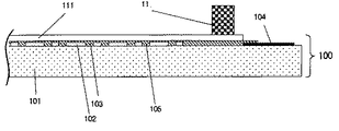
図1は、本発明に係わる放射線検出装置の一実施形態を示す断面図である。図1において、101はガラス等からなる基板、102は光電変換素子であり、複数の光電変換素子102及びTFT(不図示)を2次元状に配置して光電変換部(受光部)を形成している。103は光電変換素子102またはTFTに接続された配線、104は配線3と接続されるボンディングパッド部などの接続リード、105は窒化シリコン等よりなるセンサー保護層(第1の保護層)、111は樹脂膜等より形成された光電変換素子102の剛性保護の役割を兼ねた蛍光体下地層(第2の保護層)である。これら構成要素101〜111によってセンサーパネル100が構成される。112は蛍光体層で、13は蛍光体層112の上面を覆う蛍光体保護層である。11は蛍光体層112の側壁に接し外周を覆うように形成された枠体(枠部材)である。また、14は反射層、15は反射層保護層である。上記構成要素13、11、14、15によって蛍光体保護部材が構成されている。接続リード104は、異方性導電接着フィルム等を用いてフレキシブル配線板等と電気的に接続され、外部の電気回路との接続がなされる。
FIG. 1 is a sectional view showing an embodiment of a radiation detection apparatus according to the present invention. In FIG. 1, 101 is a substrate made of glass or the like, 102 is a photoelectric conversion element, and a plurality of
基板101は、光電変換素子102、配線103、及びTFT(不図示)からなる光電変換部(受光部)が形成されるものであり、材料として、ガラス、耐熱性プラスチック等を好適に用いることができる。
The
光電変換素子102は蛍光体層112によって放射線から変換された光を電荷に変換するものであり、例えば、アモルファスシリコンなどの材料を用いることが可能である。光電変換素子102の構成は特に限定されず、MIS型センサー、PIN型センサー、TFT型センサー等適宜用いることができる。
The
配線103は、光電変換素子102で光電変換された信号をTFTを介して読み出すための信号配線の一部や、光電変換素子に電圧(Vs)を印加するバイアス配線、又はTFTを駆動するための駆動配線を示す。光電変換素子102で光電変換された信号はTFTによって読み出され、信号配線を介して信号処理回路に出力される。また行方向に配列されたTFTのゲートは行ごとに駆動配線に接続され、TFT駆動回路により行毎にTFTが選択される。
The
センサー保護層(第1の保護層)105としては、SiNやTiO2 、LiF、Al2 O3 、MgO等の他、ポリフェニレンサルファイド樹脂、フッ素樹脂、ポリエーテルエーテルケトン樹脂、液晶ポリマー、ポリエーテルニトリル樹脂、ポリスルホン樹脂、ポリエーテルサルホン樹脂、ポリアリレート樹脂、ポリアミドイミド樹脂、ポリエーテルイミド樹脂、ポリイミド樹脂、エポキシ樹脂、シリコーン樹脂等が挙げられる。特に保護層は、放射線照射時に蛍光体層112によって変換された光が通過することから、蛍光体層112が放出する光の波長において高い透過率を示すものが望ましい。
Examples of the sensor protective layer (first protective layer) 105 include SiN, TiO 2 , LiF, Al 2 O 3 , MgO, polyphenylene sulfide resin, fluororesin, polyether ether ketone resin, liquid crystal polymer, polyether nitrile. Examples thereof include resins, polysulfone resins, polyether sulfone resins, polyarylate resins, polyamideimide resins, polyetherimide resins, polyimide resins, epoxy resins, and silicone resins. In particular, the protective layer preferably has a high transmittance at the wavelength of the light emitted from the
蛍光体下地層(第2の保護層)111としては、蛍光体層形成工程での熱プロセス(柱状結晶構造を有する蛍光体層の場合、例えば200℃以上)に耐える材料であればいずれの材料でも良く、例えば、ポリアミドイミド樹脂、ポリエーテルイミド樹脂、ポリイミド樹脂、エポキシ樹脂、シリコーン樹脂等が挙げられる。
枠体(枠部材)11は、蛍光体層112の蒸着時に非蒸着面を覆うホルダーとセンサーパネルの非蒸着面表面との間に設けられて密着し、ホルダーとセンサーパネルとの近接を防止する。また、枠体11は蛍光体層の側面に接し、蛍光体層112の防湿保護の機能する。したがって、枠体11は蛍光体層形成領域を規定するとともに蛍光体保護層として機能する。枠体11の材料としては、例えば、シリコーン樹脂、アクリル樹脂、エポキシ樹脂などの一般的な有機封止材料を用いることができるが、特に水分透過率の低い樹脂で蛍光体下地層111と同様に、蛍光体層形成工程での熱プロセス(柱状結晶構造を有する蛍光体層の場合、例えば200℃以上)に耐える材料が望ましい。
As the phosphor underlayer (second protective layer) 111, any material can be used as long as it can withstand the thermal process in the phosphor layer forming step (for example, 200 ° C. or more in the case of a phosphor layer having a columnar crystal structure). For example, a polyamideimide resin, a polyetherimide resin, a polyimide resin, an epoxy resin, a silicone resin, and the like can be given.
The frame (frame member) 11 is provided between the holder that covers the non-deposition surface and the non-deposition surface of the sensor panel when the
蛍光体層112は、放射線を光電変換素子102が感知可能な光に変換するものであり、柱状結晶構造を有する蛍光体が好ましい。柱状結晶構造を有する蛍光体は、蛍光体で発生した光が柱状結晶内を伝搬するので光散乱が少なく、解像度を向上させることができる。ただし、蛍光体層112としては、柱状結晶構造を有する蛍光体以外の材料を用いてもよい。柱状結晶構造を有する蛍光体層111の材料としては、ハロゲン化アルカリを主成分とする材料が好適に用いられる。例えば、CsI:Tl、CsI:Na、CsBr:Tl、NaI:Tl、LiI:Eu、KI:Tl等が用いられる。その作製方法は、例えばCsI:Tlでは、CsIとTlIを同時に蒸着することで形成できる。
蛍光体保護層13は、蛍光体層112に対して、外気からの水分の侵入を防止する防湿保護機能及び衝撃により構造破壊を防止する衝撃保護機能を有するものである。蛍光体層112として柱状結晶構造を有する蛍光体を用いる場合、蛍光体保護層13の厚さは20〜200μmが好ましい。20μm以下では、蛍光体層112表面の凹凸、及びスプラッシュ欠陥を完全に被覆することができず、防湿保護機能が低下する恐れがある。一方、200μmを超えると蛍光体層112で発生した光もしくは反射層で反射された光の蛍光体保護層13内での散乱が増加し、取得される画像の解像度及びMTF(Modulation Transfer Fanction)が低下する恐れがある。蛍光体保護層13の材料としては、例えば、シリコーン樹脂、アクリル樹脂、エポキシ樹脂などの一般的な有機封止材料や、またポリエステル系、ポリオレフィン系、ポリアミド系等のホットメルト樹脂などを用いることができるが、特に水分透過率の低い樹脂が望ましい。蛍光体保護層13としては、CVD蒸着で形成するポリパラキシリレンの有機膜が好適に用いられる。また、蛍光体保護層13として後述するホットメルト樹脂を好適に用いることができる。
The
The phosphor
反射層14は、蛍光体層112で変換して発せられた光のうち、光電変換素子102と反対側に進行した光を反射して光電変換素子102に導くことにより、光利用効率を向上させる機能を有するものである。また、反射層14は、光電変換素子102に蛍光体層112で発生された光以外の外部光線を遮断し、光電変換素子102にノイズが入ることを防止する機能を更に有する。反射層14としては、金属箔または金属薄膜を用いることが好ましく、反射層14の厚さは1〜100μmが好ましい。1μmより薄いと反射層14の形成時にピンホール欠陥が発生しやすく、また遮光性に劣る。一方、100μmを超えると、放射線の吸収量が大きく被撮影者が被爆する線量の増加につながる恐れがあり、また、蛍光体層112とセンサーパネルの表面との段差を隙間無く覆うことが困難となる恐れがある。反射層112の材料としては、アルミニウム、金、銅、アルミ合金、などの金属材料を用いることができるが、特に反射特性の高い材料としては、アルミニウム、金が好ましい。
The
反射層保護層15は、反射層14の衝撃による破壊、及び水分による腐食を防止する機能を有し、樹脂フィルムを用いることが好ましい。反射層保護層15の材料としては、ポリエチレンテレフタレート、ポリカーボネート、塩化ビニル、ポリエチレンナフタレート、ポリイミド、などのフィルム材料を用いることが好ましい。反射層保護層15の厚さは10〜100μmが好ましい。本実施の形態においては、蛍光体保護層13、反射層14、及び反射層保護層15によって蛍光体保護部材が構成され、蛍光体層112及び蛍光体保護部材によって波長変換体が構成されている。
蛍光体保護層13として用いられるホットメルト樹脂は、水や溶剤を含まない、室温で固体であり、100%不揮発性の熱可塑性材料からなる接着性樹脂と定義される(Thomas.p.Flanagan,Adhesive Age,9,No3,28(1996))。ホットメルト樹脂は、樹脂温度が上昇すると溶融し、樹脂温度が低下すると固化されるものである。ホットメルト樹脂は、加熱溶融状態で、他の有機材料、および無機材料に接着性をもち、常温で固体状態となり接着性を持たないものである。また、ホットメルト樹脂は極性溶媒、溶剤、および水を含んでいないので、蛍光体層112(例えば、ハロゲン化アルカリからなる柱状結晶構造を有する蛍光体層)に接触しても蛍光体層を溶解しないため、蛍光体保護層13として使用され得る。ホットメルト樹脂は、熱可塑性樹脂を溶剤に溶かし溶媒塗布法によって形成された溶剤揮発硬化型の接着性樹脂とは異なる。またエポキシ等に代表される化学反応によって形成される化学反応型の接着性樹脂とも異なる。
ホットメルト樹脂材料は主成分であるベースポリマー(ベース材料)の種類によって分類され、ポリオレフィン系、ポリエステル系、ポリアミド系等を用いることができる。蛍光体保護層13として、防湿性が高く、また蛍光体から発生する可視光線を透過する光透過性が高いことが重要である。蛍光体保護層13として必要とされる防湿性を満たすホットメルト樹脂としてポリオレフィン系樹脂、ポリエステル系樹脂が好ましい。特に吸湿率が低いポリオレフィン樹脂を用いることが好ましい。また光透過性の高い樹脂として、ポリオレフィン系樹脂が好ましい。したがって蛍光体保護層13としてポリオレフィン系樹脂をベースにしたホットメルト樹脂がより好ましい。ポリオレフィン樹脂は、エチレン−酢酸ビニル共重合体、エチレン−アクリル酸共重合体、エチレン−アクリル酸エステル共重合体、エチレン−メタクリル酸共重合体、エチレン−メタクリル酸エステル共重合体および、アイオノマー樹脂から選ばれる少なくとも1種を主成分として含有することが好ましい。エチレン酢酸ビニル共重合体を主成分とするホットメルト樹脂としてヒロダイン7544(ヒロダイン工業製)、エチレン−アクリル酸エステル共重合体を主成分とするホットメルト樹脂としてO−4121(倉敷紡績製)、エチレン−メタクリル酸エステル共重合体を主成分とするホットメルト樹脂としてW−4110(倉敷紡績製)、エチレン−アクリル酸エステル共重合体を主成分とするホットメルト樹脂としてH−2500(倉敷紡績製)、エチレン−アクリル酸共重合体を主成分とするホットメルト樹脂としてP−2200(倉敷紡績製)、エチレン−アクリル酸エステル共重合体を主成分とするホットメルト樹脂としてZ−2(倉敷紡績製)等を用いることができる。
図2、図3、図4は、図1の本発明の放射線検出装置の製造方法を示す断面図である。
構成要素101〜105、111によって構成されたセンサーパネル100(図2)に、上述した有機材料よりなる枠体11を二次元配置された光電変換素子部を囲むよう枠状にディスペンス装置やスクリーン印刷装置等により形成する(図3)。
次に、アルカリハライドよりなる柱状構造結晶の蛍光体(例えば、CsI:Tl、タリウム活性化沃化セシウム)よりなる蛍光体層112を蛍光体層形成蒸着装置によって形成する。このとき、センサーパネル100は蛍光体蒸着ステージ上に載置され、接続リード104等の非蛍光体層形成面は装置にセットする際のホルダー21と枠体11によりマスキングされ、蛍光体層112は枠状に形成した枠体11の内側の蛍光体下地層111上に形成される(図4)。形成された蛍光体層112上に蛍光体保護層13を形成する。このとき、蛍光体保護層13は蛍光体層112の表面と密着し、また外周部においては枠体11の表面に接するよう形成され、蛍光体層112は枠体11と蛍光体保護層13で覆われる。次に反射層保護層上15に予め反射層14が形成されたシートを枠体11と蛍光体保護層13上に形成し、本実施例の放射線検出装置(図1)を作製する。
以下、蛍光体層112上に蛍光体保護層を形成する方法について図5を用いて説明する。
The reflective layer
The hot melt resin used as the phosphor
Hot-melt resin materials are classified according to the type of base polymer (base material) that is the main component, and polyolefin-based, polyester-based, polyamide-based, and the like can be used. It is important for the phosphor
2, 3 and 4 are cross-sectional views showing a method for manufacturing the radiation detection apparatus of the present invention shown in FIG.
Dispensing device or screen printing in a frame shape so as to surround the photoelectric conversion element part in which the
Next, a
Hereinafter, a method of forming a phosphor protective layer on the
まず図5(a)に示すように、溶融されたホットメルト樹脂401をタンク(不図示)及びダイコータ400内に準備し、センサーパネル100の枠体11上の所定の位置に配置する。次に図5(b)に示すように、枠体11の所定の位置より溶融されたホットメルト樹脂401を射出しながらダイコータ400を走査して枠体11及び蛍光体層112の上面に塗布する。次に図5(c)に示すように、枠体11及び蛍光体層112にホットメルト樹脂を塗布して被覆し、放熱硬化し、蛍光体保護層13を形成し、さらに反射層保護層上15に予め反射層14が形成されたシートを枠体11と蛍光体保護層13上に形成して終了する。
First, as shown in FIG. 5A, a molten
反射層保護層上15に反射層14、蛍光体保護層13が形成された蛍光体保護シートを作成し、この蛍光体保護シートを熱ラミネートで蛍光体層7の表面に形成することもできる。
すなわち、図6(a)、(b)に示されるように、溶融されたホットメルト樹脂をタンク402、403及びダイコータ409内に準備するとともに、ロール状に準備された金属箔または金属蒸着膜等の反射層14及び反射層保護層15の積層からなる積層シートを準備し、しわ取りロール404,405によってしわを伸ばされた積層シート上に成形ロール406,407間で溶融されたホットメルト樹脂401を押し出しコート法により塗布し、成形ロール407により成形後、冷却ロール408にて冷却硬化し、切断手段410にて所定のサイズに切り出す。こうして、金属箔または金属蒸着膜14上にホットメルト樹脂からなる蛍光体保護層13を形成し、図6(b)で示される蛍光体保護シートを形成する。次に図7(a)に示すように、得られた蛍光体保護シートをセンサーパネル100の蛍光体下地層111上及び蛍光体層112上に重ねて、熱ラミネートローラ411によってホットメルト樹脂の溶融温度以上にホットメルト樹脂を加熱して溶融し、熱ラミネートローラ411及び搬送ローラ412を用いて放射線検出装置を移動させて、枠体11上の蛍光体保護シート上の所定の開始位置から蛍光体層112上を熱ラミレートローラ411が相対的に移動するようにして所定の開始位置から他端の枠体11上まで加熱圧着する。ここで放射線検出装置を平面で90°回転させて再度、枠体11上の蛍光体保護シート上の所定の開始位置から蛍光体層112上を熱ラミレートローラ27が相対的に移動するようにして所定の開始位置から他の枠体11上まで加熱圧着する。こうして、図7(b)に示すように、蛍光体保護シートが蛍光体層112及び枠体11上に密着される。熱ラミネートロールの温度は90〜180℃の範囲で調整する。熱ラミネートロールの回転速度は0.01〜1m/minの範囲で調整する。熱ラミネートロールの押圧力は、1〜50kg/cm2の範囲で調整する。
A phosphor protective sheet in which the
That is, as shown in FIGS. 6 (a) and 6 (b), a molten hot melt resin is prepared in the
2次元光検出器として、ガラス基板上にアモルファスシリコンを用いたフォトセンサーとTFTからなる光電変換部を形成した場合について説明したが、CCDやCMOSセンサ等を2次元状に配置した撮像素子を形成した半導体単結晶基板上に下地層、蛍光体層を配置することで同様の放射線検出装置を構成することができる。 As a two-dimensional photodetector, the case where a photoelectric conversion unit comprising a photosensor using amorphous silicon and a TFT is formed on a glass substrate has been described. However, an imaging device in which a CCD, a CMOS sensor, etc. are arranged in a two-dimensional form is formed. A similar radiation detection apparatus can be configured by disposing an underlayer and a phosphor layer on the semiconductor single crystal substrate.
次に、本発明の放射線検出装置を実施例に基づいて詳細に説明する。 Next, the radiation detection apparatus of the present invention will be described in detail based on examples.
図2に示すように、ガラス等の基板101上の非晶質シリコンから成る半導体薄膜上にフォトセンサー(光電変換素子)102とTFTからなる光電変換部(受光部)および配線103を形成し、その上にSiNx よりなるセンサー保護層(第1の保護層)105と、さらにポリイミド樹脂を硬化した蛍光体下地層111を形成してセンサーパネル100を作製した。
As shown in FIG. 2, a photosensor (photoelectric conversion element) 102 and a photoelectric conversion part (light receiving part) made of TFT and
次に、図3に示すように蛍光体下地層111上にエポキシ樹脂よりなる枠体11をセンサーパネル上に二次元配置された光電変換部を囲むよう枠状にディスペンス装置により幅2mm、高さ0.5mmで塗布硬化形成し、その後、図4に示すように、アルカリハライドよりなる柱状構造結晶の蛍光体(例えば、CsI:Tl、タリウム活性化沃化セシウム)よりなる蛍光体層112を蛍光体層形成蒸着装置によって形成した。このとき、接続リード104等の非蛍光体層形成面上にマスキングの役目を担う装置のホルダー部(マスク部材)21が配置され、ホルダー部21はセンサーパネル上に形成した枠体11に密着させるようセットし(蛍光体層の形成領域以外をマスクするように、ホルダー部が枠部材で支持される)、蛍光体層112を蒸着させた。蛍光体層112は厚さ0.5mm形成し、二次元に配置されている光電変換部の上面を覆うよう蛍光体下地層111上に形成され、また、枠体11の側壁に接し同一の高さに形成させた(図4)。
Next, as shown in FIG. 3, a
更に、予めPETの反射層保護層15に反射層14としてAl膜が形成されたフィルム状シートの反射層形成面にポリオレフィン樹脂からなるホットメルト樹脂からなる蛍光体保護層13をヒートローラーを用い転写接着させ3層のフィルム状シート(図6)とし、3層のフィルムシートを図4まで作製したセンサーパネルの蛍光体層112を覆い且つ3層フィルムシートの外周が枠体11の上面にかかるように蛍光体保護層13の面と対向するよう配置し、ヒートローラーにより加熱押圧し蛍光体保護層13の溶着により配置固定させる(図7)。このとき、蛍光体層112は枠体11と蛍光体保護層13が接して覆われる。以上により本実施例の放射線検出装置(図1)を作製する。
Furthermore, the phosphor
本実施例のような構成においては、センサーパネル上に枠体を設け蛍光体層を蒸着形成しているので、静電気による光電変換部や配線の影響を防止でき歩留まりの高く、安定した生産ができ、また、本実施例の放射線検出装置は、センサーパネル作成後の工程において高価で形成レートの低いCVD等の真空蒸着装置を必要としないため、構成要素を安価な装置により短時間で作製でき、低コストな放射線検出装置が得られた。 In the configuration as in this example, the frame is provided on the sensor panel and the phosphor layer is formed by vapor deposition. Therefore, the influence of the photoelectric conversion part and wiring due to static electricity can be prevented, and the yield can be high and stable production can be achieved. In addition, since the radiation detection apparatus of the present embodiment does not require a vacuum deposition apparatus such as CVD having a low and low formation rate in the process after the sensor panel is created, the components can be produced in a short time with an inexpensive apparatus, A low-cost radiation detection apparatus was obtained.
図8は、本発明第2の実施例の放射線検出装置を示す模式的部分断面図である。尚、前述の従来例の説明に用いた図11及び第1の実施例の説明で用いた図1〜図4と同一または同等のものには、同一番号を付し、説明を簡略あるいは省略する。
図8の放射線撮像装置も第1の実施例と同様に枠部材11を二次元配置された光電変換部を囲むよう枠状にディスペンス装置やスクリーン印刷装置等により形成した後に、真空蒸着ホルダーを設置し蛍光体層112を形成し、その後同様に蛍光体保護層13を蛍光体層112及び枠部材11の表面と接するよう配置固定している。
図8で明らかなように本実施例では、センサーパネル100上に形成する枠部材11がセンサーパネル上の蛍光体下地層111と第1の保護層105の双方に接するように配し形成させている。本実施例の放射線検出装置も第1の実施例と同様の効果が得られた。
FIG. 8 is a schematic partial sectional view showing a radiation detecting apparatus according to the second embodiment of the present invention. 11 that are the same as or equivalent to those in FIG. 11 used in the description of the above-described conventional example and in the description of the first embodiment are denoted by the same reference numerals, and the description thereof is simplified or omitted. .
As in the first embodiment, the radiation imaging apparatus of FIG. 8 is also formed with a vacuum evaporation holder after the
As is apparent from FIG. 8, in this embodiment, the
センサーパネル上に形成される枠11の形成高さと蛍光体層112の形成高さを同一に形成しているがこれに限るものではなく、蛍光体層112の高さを枠部材11より高くもしくは低く形成し構成することもできる。
図9本発明の第3の実施例の放射線検出装置の放射線検出装置を示す模式的部分断面図であり、本実施例は、蛍光体層112を枠部材11より高く形成した場合の例である。
この場合、蛍光体保護層13を、図7に示すようにヒートローラーで加熱押圧し形成するときに、枠部材11の表面が蛍光体層112より低くなってしまっているので、ヒートローラーの押し圧が弱くなり枠部材11の表面と蛍光体保護層13との接着性が劣る傾向ができてしまうが、その後に図10に示すように、枠部材11表面上の蛍光体保護層13をバータイプの加熱加圧ヘッド413にて再度適正の加熱圧着(ホットプレス)し、ホットプレス部300を形成することで接着性を改善させている。
無論、本実施例のホットプレス部300は、実施例1(図1)並びに実施例2(図8)で説明した放射線検出装置の枠部材上に同様に形成できる。
ここで、ホットプレスの作用効果について説明すると、蛍光体保護層13や、蛍光体保護層13,反射層14,反射層保護層15を有する蛍光体保護シートをセンサーパネルに貼り合せる際の温度は、樹脂の融解温度相当で行うが、融解の際に微小な気泡が発生する場合があり、その気泡によって部分的に密着力が小さくなる。蛍光体保護層5や蛍光体保護シートの端部周辺でも同様の問題が考えられ、密着力が低下すると、ホットメルト樹脂とセンサーパネルとの界面からの水分の浸入のおそれがあり、それによって柱状結晶構造を有する蛍光体層の潮解をもたらし、発光量、分解特性の劣化をもたらすことになるので、更なる密着力の向上が望まれる。
蛍光体保護層13の端部におけるホットプレスは、耐湿性の向上を目的とし、樹脂の融解温度よりやや高めの加熱および加圧を行い、加熱によって樹脂を十分に融解させ、気泡が発生しても加圧によって外部に押し出すことによって残気泡による密着力低下を防止し、さらに加圧によって端部の接着層厚を薄くすることによって、外部からの水分侵入ルートをせばめることが可能になる。更に、上記ホットプレスにより枠部材11とホットメルト樹脂からなる蛍光体保護層13の密着力が向上し、外力による剥離の防止や耐湿性の向上を行うことができる。
300がホットプレス部(ヒートシール部)であり、ホットメルト樹脂の層の厚さが薄くなっている。ホットプレス処理としては、例えば圧力1〜10kg/cm2、温度はホットメルト樹脂の溶融開始温度より10〜50℃以上の温度で1〜60秒間行われる。
Although the formation height of the
9 is a schematic partial cross-sectional view showing a radiation detection apparatus of a radiation detection apparatus according to a third embodiment of the present invention, which is an example in the case where the
In this case, when the phosphor
Of course, the hot press part 300 of the present embodiment can be similarly formed on the frame member of the radiation detection apparatus described in the first embodiment (FIG. 1) and the second embodiment (FIG. 8).
Here, the effect of hot pressing will be described. The temperature at which the phosphor
The hot press at the end of the phosphor
Reference numeral 300 denotes a hot press part (heat seal part), and the thickness of the hot melt resin layer is thin. As the hot press treatment, for example, the pressure is 1 to 10 kg / cm 2 and the temperature is 10 to 50 ° C. or more from the melting start temperature of the hot melt resin for 1 to 60 seconds.
図11は本発明による放射線検出装置のX線診断システムへの応用例を示したものである。 FIG. 11 shows an application example of the radiation detection apparatus according to the present invention to an X-ray diagnostic system.
X線チューブ6050で発生したX線6060は患者あるいは被験者6061の胸部6062を透過し、図11に示したような放射線検出装置(イメージセンサ)6040に入射する。この入射したX線には患者6061の体内部の情報が含まれている。X線の入射に対応してシンチレーター(蛍光体層)は発光し、これをセンサーパネルの光電変換素子が光電変換して、電気的情報を得る。この情報はディジタルに変換され信号処理手段となるイメージプロセッサ6070により画像処理され制御室の表示手段となるディスプレイ6080で観察できる。
また、この情報は電話回線6090等の伝送処理手段により遠隔地へ転送でき、別の場所のドクタールームなどの表示手段となるディスプレイ6081に表示もしくは光ディスク等の記録手段に保存することができ、遠隔地の医師が診断することも可能である。また記録手段となるフィルムプロセッサ6100によりフィルム6110に記録することもできる。 Further, this information can be transferred to a remote location by transmission processing means such as a telephone line 6090 and can be displayed on a display 6081 serving as a display means such as a doctor room in another place or stored in a recording means such as an optical disk. It is also possible for a local doctor to make a diagnosis. Moreover, it can also record on the film 6110 by the film processor 6100 used as a recording means.
以上説明したように、本発明は、医療用のX線センサ等に応用することが可能であるが、非破壊破壊検査等のそれ以外の用途に応用した場合にも有効である。 As described above, the present invention can be applied to medical X-ray sensors and the like, but is also effective when applied to other uses such as non-destructive destructive inspection.
11 枠体
100 センサーパネル
101 基板
102 光電変換素子
103 配線
104 接続リード
105 センサー保護層(第1の保護層)
111 蛍光体下地層(第2の保護層)
112 蛍光体層
13、113 蛍光体保護層
14、114 反射層
15、115 反射層保護層
116 保護樹脂
117 封止樹脂
300 ホットプレス部
11
111 phosphor underlayer (second protective layer)
DESCRIPTION OF
Claims (5)
少なくとも該受光部上に配置された、放射線を前記光電変換素子が感知可能な光に変換する、柱状結晶構造を有する蛍光体層と、
該蛍光体層を被覆し前記センサーパネルと接する、ホットメルト樹脂からなる蛍光体保護部材と、を有する放射線検出装置において、
前記蛍光体保護部材は、前記蛍光体層と前記電気接続部との間の前記センサーパネル上に、前記蛍光体層の側面と接して配置された枠部材と、前記蛍光体層の上面を被覆し、且つ前記枠部材の上面と密着して配置された蛍光体保護層と、を有し、
前記蛍光体保護層は前記枠部材の上面において加熱圧着された加熱圧着部を含み、前記蛍光体保護層の前記加熱圧着部の膜厚は前記加熱圧着部以外の膜厚より薄いことを特徴とする放射線検出装置。 A light receiving unit composed of a plurality of photoelectric conversion elements arranged two-dimensionally on the substrate, and a plurality of photoelectric conversion elements electrically connected to the photoelectric conversion elements in each row or each column of the light receiving unit and arranged outside the light receiving unit A sensor panel comprising:
A phosphor layer having a columnar crystal structure, which is disposed on at least the light receiving portion and converts radiation into light that can be sensed by the photoelectric conversion element;
In a radiation detection apparatus having a phosphor protective member made of a hot melt resin that covers the phosphor layer and is in contact with the sensor panel,
The phosphor protection member covers a frame member disposed in contact with a side surface of the phosphor layer on the sensor panel between the phosphor layer and the electrical connection portion, and covers an upper surface of the phosphor layer. and, and have a, and a phosphor protective layer disposed in close contact with the upper surface of the frame member,
The phosphor protective layer includes a thermocompression bonding part that is thermocompression bonded on the upper surface of the frame member, and the film thickness of the thermocompression bonding part of the phosphor protective layer is thinner than the film thickness other than the thermocompression bonding part. A radiation detection device.
前記放射線検出装置からの信号を処理する信号処理手段と、
前記信号処理手段からの信号を記録するための記録手段と、
前記信号処理手段からの信号を表示するための表示手段と、
前記信号処理手段からの信号を伝送するための伝送処理手段と、
前記放射線を発生させるための放射線源とを具備することを特徴とする放射線検出システム。 The radiation detection apparatus according to claim 1 ;
Signal processing means for processing a signal from the radiation detection device;
Recording means for recording a signal from the signal processing means;
Display means for displaying a signal from the signal processing means;
Transmission processing means for transmitting a signal from the signal processing means;
A radiation detection system comprising: a radiation source for generating the radiation.
少なくとも該受光部上に配置された、放射線を前記光電変換素子が感知可能な光に変換する蛍光体層と、
を有する放射線検出装置の製造方法であって、
前記受光部と前記電気接続部との間の前記センサーパネル上に枠部材を形成する工程と、
前記枠部材で囲まれた前記センサーパネル上に蒸着により柱状結晶構造を有する前記蛍光体層を配する工程と、
前記蛍光体層の上面を被覆し、且つ前記枠部材の上面と密着するホットメルト樹脂からなる蛍光体保護層を形成する工程と、
前記枠部材の上面において、前記蛍光体保護層を加熱圧着手段で加熱圧着して、前記蛍光体保護層の加熱圧着部の膜厚を前記加熱圧着部以外の膜厚より薄くする工程と、
を有することを特徴とする放射線検出装置の製造方法。 A light receiving unit composed of a plurality of photoelectric conversion elements arranged two-dimensionally on the substrate, and a plurality of photoelectric conversion elements electrically connected to the photoelectric conversion elements in each row or each column of the light receiving unit and arranged outside the light receiving unit A sensor panel comprising:
A phosphor layer that is disposed on at least the light receiving section and converts radiation into light that can be sensed by the photoelectric conversion element;
A method for manufacturing a radiation detection apparatus comprising:
Forming a frame member on the sensor panel between the light receiving portion and the electrical connection portion;
Disposing the phosphor layer having a columnar crystal structure by vapor deposition on the sensor panel surrounded by the frame member;
Forming a phosphor protective layer made of a hot melt resin that covers the upper surface of the phosphor layer and is in close contact with the upper surface of the frame member;
On the upper surface of the frame member, the phosphor protective layer is thermocompression bonded by thermocompression bonding means, and the film thickness of the thermocompression bonding portion of the phosphor protective layer is made thinner than the film thickness other than the thermocompression bonding portion;
The manufacturing method of the radiation detection apparatus characterized by having.
Priority Applications (2)
| Application Number | Priority Date | Filing Date | Title |
|---|---|---|---|
| JP2004233423A JP4266898B2 (en) | 2004-08-10 | 2004-08-10 | Radiation detection apparatus, manufacturing method thereof, and radiation imaging system |
| US11/198,229 US7391029B2 (en) | 2004-08-10 | 2005-08-08 | Radiation detecting apparatus, producing method therefor and radiation image pickup system |
Applications Claiming Priority (1)
| Application Number | Priority Date | Filing Date | Title |
|---|---|---|---|
| JP2004233423A JP4266898B2 (en) | 2004-08-10 | 2004-08-10 | Radiation detection apparatus, manufacturing method thereof, and radiation imaging system |
Publications (3)
| Publication Number | Publication Date |
|---|---|
| JP2006052986A JP2006052986A (en) | 2006-02-23 |
| JP2006052986A5 JP2006052986A5 (en) | 2007-09-27 |
| JP4266898B2 true JP4266898B2 (en) | 2009-05-20 |
Family
ID=35799127
Family Applications (1)
| Application Number | Title | Priority Date | Filing Date |
|---|---|---|---|
| JP2004233423A Expired - Fee Related JP4266898B2 (en) | 2004-08-10 | 2004-08-10 | Radiation detection apparatus, manufacturing method thereof, and radiation imaging system |
Country Status (2)
| Country | Link |
|---|---|
| US (1) | US7391029B2 (en) |
| JP (1) | JP4266898B2 (en) |
Families Citing this family (60)
| Publication number | Priority date | Publication date | Assignee | Title |
|---|---|---|---|---|
| US7315027B2 (en) * | 2003-10-22 | 2008-01-01 | Canon Kabushiki Kaisha | Radiation detection device, scintillator panel, method of making the same, making apparatus, and radiation image pick-up system |
| JP4594188B2 (en) * | 2004-08-10 | 2010-12-08 | キヤノン株式会社 | Radiation detection apparatus and radiation detection system |
| WO2006016505A1 (en) * | 2004-08-10 | 2006-02-16 | Canon Kabushiki Kaisha | Radiation detecting apparatus, scintillator panel, their manufacturing method and radiation detecting system |
| JP4208790B2 (en) * | 2004-08-10 | 2009-01-14 | キヤノン株式会社 | Manufacturing method of radiation detection apparatus |
| JP2007155662A (en) | 2005-12-08 | 2007-06-21 | Canon Inc | Radiation detector and radiation imaging system using the same |
| JP4579894B2 (en) * | 2005-12-20 | 2010-11-10 | キヤノン株式会社 | Radiation detection apparatus and radiation detection system |
| JP4920994B2 (en) * | 2006-03-02 | 2012-04-18 | キヤノン株式会社 | Scintillator panel, radiation detection apparatus and radiation detection system |
| JP5089195B2 (en) * | 2006-03-02 | 2012-12-05 | キヤノン株式会社 | Radiation detection apparatus, scintillator panel, radiation detection system, and method for manufacturing radiation detection apparatus |
| JP2008014859A (en) * | 2006-07-07 | 2008-01-24 | Fujifilm Corp | Radiation image conversion panel and method for manufacturing radiation image conversion panel |
| WO2008053642A1 (en) * | 2006-10-30 | 2008-05-08 | Konica Minolta Medical & Graphic, Inc. | Scintilator plate, scintillator panel, and radiation flat panel detector employing them |
| DE102007008381A1 (en) * | 2007-02-21 | 2008-08-28 | Robert Bosch Gmbh | Radiation sensing element, has substrate and laminar sensor structure that is arranged by substrate in level, and lead structure that is arranged between substrate and sensor structure in another level |
| JP5476991B2 (en) * | 2007-03-27 | 2014-04-23 | コニカミノルタ株式会社 | Radiation image conversion panel, manufacturing method therefor, and X-ray imaging system |
| JP5052181B2 (en) * | 2007-03-30 | 2012-10-17 | 富士フイルム株式会社 | Radiation detector |
| JP5004848B2 (en) * | 2007-04-18 | 2012-08-22 | キヤノン株式会社 | Radiation detection apparatus and radiation detection system |
| JP4834614B2 (en) * | 2007-06-12 | 2011-12-14 | キヤノン株式会社 | Radiation detection apparatus and radiation imaging system |
| JP5073399B2 (en) * | 2007-07-27 | 2012-11-14 | 富士フイルム株式会社 | Radiation detector |
| JP4940098B2 (en) * | 2007-10-23 | 2012-05-30 | 富士フイルム株式会社 | Image detector |
| KR100964654B1 (en) | 2008-02-20 | 2010-06-22 | 주식회사바텍 | A large area x-ray detector and method for fabricating the same |
| KR100936476B1 (en) | 2008-02-22 | 2010-01-13 | 주식회사바텍 | Method for fabricating large area x-ray detector |
| JP5185003B2 (en) * | 2008-07-25 | 2013-04-17 | 浜松ホトニクス株式会社 | Radiation detector |
| WO2011055508A1 (en) * | 2009-11-05 | 2011-05-12 | 株式会社島津製作所 | Radiation detection device |
| KR101202787B1 (en) | 2009-12-02 | 2012-11-19 | (주)바텍이우홀딩스 | X-ray detector and Method for the same |
| US9995831B2 (en) * | 2010-04-26 | 2018-06-12 | Koninklijke Philips N.V. | X-ray detector with improved spatial gain uniformity and resolution and method of fabricating such X-ray detector |
| JP5607426B2 (en) | 2010-05-28 | 2014-10-15 | キヤノン株式会社 | Radiation detection apparatus and radiation imaging system |
| JP5562134B2 (en) | 2010-06-17 | 2014-07-30 | キヤノン株式会社 | Radiation detection apparatus, manufacturing method thereof, and radiation imaging system |
| JP5665494B2 (en) | 2010-06-24 | 2015-02-04 | キヤノン株式会社 | Radiation detection apparatus and radiation imaging system |
| KR101216587B1 (en) | 2010-08-23 | 2012-12-31 | 주식회사 아비즈알 | Scintillator panel and x-ray image sensor including the same |
| KR101253586B1 (en) * | 2010-08-25 | 2013-04-11 | 삼성전자주식회사 | Phosphor film, method of manufacturing the same, method of coating phosphor layer on an LED chip, method of manufacturing LED package and LED package manufactured thereof |
| JP2012098175A (en) * | 2010-11-02 | 2012-05-24 | Sony Corp | Radiation detection element and manufacturing method thereof, radiation detection module, and radiation image diagnostic device |
| JP5680943B2 (en) * | 2010-11-16 | 2015-03-04 | キヤノン株式会社 | Scintillator, radiation detection device and radiation imaging device |
| JP5629593B2 (en) * | 2011-02-01 | 2014-11-19 | 株式会社東芝 | Radiation detector |
| JP2012172971A (en) * | 2011-02-17 | 2012-09-10 | Konica Minolta Medical & Graphic Inc | Scintillator panel, manufacturing method thereof, flat panel detector and manufacturing method thereof |
| JP2012177623A (en) * | 2011-02-25 | 2012-09-13 | Fujifilm Corp | Radiation image detector and method for manufacturing radiation image detector |
| JP5728285B2 (en) * | 2011-04-27 | 2015-06-03 | 富士フイルム株式会社 | Radiation image conversion panel, radiation image conversion panel manufacturing method, and radiation image detection apparatus |
| KR101266554B1 (en) * | 2011-05-09 | 2013-05-27 | 주식회사 아비즈알 | A scintillator panel and a method for manufacturing the sintillator panel |
| JP2013029384A (en) | 2011-07-27 | 2013-02-07 | Canon Inc | Radiation detection device, manufacturing method thereof, and radiation detection system |
| JP2013174465A (en) * | 2012-02-23 | 2013-09-05 | Canon Inc | Radiation detection device |
| JP6000680B2 (en) | 2012-06-20 | 2016-10-05 | キヤノン株式会社 | Radiation detection apparatus, manufacturing method thereof, and imaging system |
| JP5997512B2 (en) | 2012-06-20 | 2016-09-28 | キヤノン株式会社 | Radiation detection apparatus and imaging system |
| JP6071283B2 (en) | 2012-07-04 | 2017-02-01 | キヤノン株式会社 | Radiation detection apparatus and manufacturing method thereof |
| US9063238B2 (en) * | 2012-08-08 | 2015-06-23 | General Electric Company | Complementary metal-oxide-semiconductor X-ray detector |
| JP6107001B2 (en) * | 2012-09-04 | 2017-04-05 | ソニー株式会社 | Scintillator and radiation detection apparatus |
| JP2014071077A (en) * | 2012-10-01 | 2014-04-21 | Canon Inc | Radiation detection device and radiation detection system |
| JP6092568B2 (en) | 2012-10-11 | 2017-03-08 | キヤノン株式会社 | Radiation detection apparatus and radiation detection system |
| JP6100045B2 (en) | 2013-03-19 | 2017-03-22 | キヤノン株式会社 | Radiation detection apparatus, radiation detection system, and method of manufacturing radiation detection apparatus |
| JP2015004560A (en) * | 2013-06-20 | 2015-01-08 | 株式会社東芝 | Radiation detector and method of manufacturing the same |
| JP5936584B2 (en) * | 2013-08-29 | 2016-06-22 | 富士フイルム株式会社 | Radiation image detection apparatus and manufacturing method |
| JP6310216B2 (en) | 2013-09-06 | 2018-04-11 | キヤノン株式会社 | Radiation detection apparatus, manufacturing method thereof, and radiation detection system |
| EP2857866B1 (en) * | 2013-10-02 | 2019-06-19 | Rayence Co., Ltd. | X-ray sensor and method of manufacturing the same |
| JP2015096823A (en) | 2013-11-15 | 2015-05-21 | 浜松ホトニクス株式会社 | Radiation detector and radiation detector manufacturing method |
| JP6478538B2 (en) | 2014-09-10 | 2019-03-06 | キヤノン株式会社 | Radiation imaging apparatus and radiation imaging system |
| JP6487263B2 (en) * | 2015-04-20 | 2019-03-20 | 浜松ホトニクス株式会社 | Radiation detector and manufacturing method thereof |
| JP6573377B2 (en) | 2015-07-08 | 2019-09-11 | キヤノン株式会社 | Radiation imaging apparatus, control method thereof, and program |
| JP6573378B2 (en) | 2015-07-10 | 2019-09-11 | キヤノン株式会社 | Radiation imaging apparatus, control method thereof, and program |
| JP6663210B2 (en) | 2015-12-01 | 2020-03-11 | キヤノン株式会社 | Radiation imaging apparatus and control method thereof |
| JP6706963B2 (en) | 2016-04-18 | 2020-06-10 | キヤノン株式会社 | Radiation imaging apparatus, radiation imaging system, and control method for radiation imaging apparatus |
| JP6778118B2 (en) | 2017-01-13 | 2020-10-28 | キヤノン株式会社 | Radiation imaging device and radiation imaging system |
| CN110869809B (en) | 2017-07-10 | 2023-07-25 | 佳能株式会社 | Radiation imaging apparatus and radiation imaging system |
| JP7030478B2 (en) | 2017-11-09 | 2022-03-07 | キヤノン株式会社 | Shooting table and radiography system |
| JP6790008B2 (en) * | 2018-03-14 | 2020-11-25 | 株式会社東芝 | Detection element and detector |
Family Cites Families (15)
| Publication number | Priority date | Publication date | Assignee | Title |
|---|---|---|---|---|
| US5107125A (en) * | 1991-03-06 | 1992-04-21 | Eastman Kodak Company | X-ray imaging screen with process for its preparation |
| US5132539A (en) | 1991-08-29 | 1992-07-21 | General Electric Company | Planar X-ray imager having a moisture-resistant sealing structure |
| US5254480A (en) * | 1992-02-20 | 1993-10-19 | Minnesota Mining And Manufacturing Company | Process for producing a large area solid state radiation detector |
| EP0762505A3 (en) * | 1995-08-28 | 1999-02-03 | Canon Kabushiki Kaisha | Apparatus for detecting radiation and method for manufacturing such apparatus |
| FR2758630B1 (en) * | 1997-01-21 | 1999-04-09 | Thomson Tubes Electroniques | PROCESS FOR SEALING A SOLID STATE RADIATION DETECTOR AND DETECTOR OBTAINED THEREBY |
| CN1844953B (en) * | 1997-02-14 | 2012-06-27 | 浜松光子学株式会社 | Radiation detection device and method of producing the same |
| US6146489A (en) * | 1998-11-19 | 2000-11-14 | General Electric Company | Method and apparatus for depositing scintillator material on radiation imager |
| KR100734546B1 (en) * | 2000-01-13 | 2007-07-04 | 하마마츠 포토닉스 가부시키가이샤 | Radiation image sensor and scintillator panel |
| US20020050570A1 (en) * | 2000-06-01 | 2002-05-02 | Yuji Isoda | Preparation of stimulable phosphor sheet |
| US6835936B2 (en) * | 2001-02-07 | 2004-12-28 | Canon Kabushiki Kaisha | Scintillator panel, method of manufacturing scintillator panel, radiation detection device, and radiation detection system |
| US6847041B2 (en) * | 2001-02-09 | 2005-01-25 | Canon Kabushiki Kaisha | Scintillator panel, radiation detector and manufacture methods thereof |
| US7315031B2 (en) * | 2002-08-14 | 2008-01-01 | Fujifilm Corporation | Radiation image storage panel |
| JP4393048B2 (en) * | 2002-09-11 | 2010-01-06 | キヤノン株式会社 | Radiation conversion board, radiation imaging apparatus, and radiation imaging system |
| JP4594188B2 (en) * | 2004-08-10 | 2010-12-08 | キヤノン株式会社 | Radiation detection apparatus and radiation detection system |
| JP4208790B2 (en) * | 2004-08-10 | 2009-01-14 | キヤノン株式会社 | Manufacturing method of radiation detection apparatus |
-
2004
- 2004-08-10 JP JP2004233423A patent/JP4266898B2/en not_active Expired - Fee Related
-
2005
- 2005-08-08 US US11/198,229 patent/US7391029B2/en not_active Expired - Fee Related
Also Published As
| Publication number | Publication date |
|---|---|
| US20060033031A1 (en) | 2006-02-16 |
| US7391029B2 (en) | 2008-06-24 |
| JP2006052986A (en) | 2006-02-23 |
Similar Documents
| Publication | Publication Date | Title |
|---|---|---|
| JP4266898B2 (en) | Radiation detection apparatus, manufacturing method thereof, and radiation imaging system | |
| JP5791281B2 (en) | Radiation detection apparatus and radiation detection system | |
| US8779369B2 (en) | Radiation detection apparatus, scintillator panel, method for manufacturing same and radiation detection system | |
| US20130308755A1 (en) | Radiation detection apparatus and radiation detection system | |
| JP4921180B2 (en) | Radiation detection apparatus and radiation imaging system | |
| JP5607426B2 (en) | Radiation detection apparatus and radiation imaging system | |
| US20110147602A1 (en) | Radiographic imaging apparatus, radiographic imaging system, and method of producing radiographic imaging apparatus | |
| KR100514546B1 (en) | Radiation Detector and its Manufacturing Method | |
| JP2006189377A (en) | Scintillator panel, radiation detector, and radiation detection system | |
| JP2001074845A (en) | Semiconductor device and radiation imaging system using the device | |
| JP5693174B2 (en) | Radiation detection apparatus and radiation detection system | |
| JP5693173B2 (en) | Radiation detection apparatus and radiation detection system | |
| JP2004281439A (en) | Radiation detecting device and its manufacturing method | |
| JP2006220439A (en) | Scintillator panel, device for detecting radiation, and its manufacturing method | |
| JP2006337184A (en) | Radiation detector | |
| JP2012154811A (en) | Scintillator panel and method for manufacturing the same, and radiation detection device | |
| JP6005092B2 (en) | Radiation detection device and method of manufacturing radiation detection device | |
| JP2007057428A (en) | Radiation detecting device and radiation imaging system | |
| JP2006052980A (en) | Radiation detection device | |
| US20140093041A1 (en) | Detecting apparatus, radiation detecting system, and method of manufacturing detecting apparatus | |
| JP2006258550A (en) | Radiation detector | |
| JP4380460B2 (en) | Radiation detection apparatus, scintillator panel, and radiation detection system | |
| JP2006052979A (en) | Radiation detection device and scintillator panel | |
| JP6995666B2 (en) | Radiation imaging device and radiation imaging system | |
| JP2006052981A (en) | Radiation detector, manufacturing method for the same and radiation detection system |
Legal Events
| Date | Code | Title | Description |
|---|---|---|---|
| A521 | Request for written amendment filed |
Free format text: JAPANESE INTERMEDIATE CODE: A523 Effective date: 20070810 |
|
| A621 | Written request for application examination |
Free format text: JAPANESE INTERMEDIATE CODE: A621 Effective date: 20070810 |
|
| RD04 | Notification of resignation of power of attorney |
Free format text: JAPANESE INTERMEDIATE CODE: A7424 Effective date: 20080207 |
|
| A131 | Notification of reasons for refusal |
Free format text: JAPANESE INTERMEDIATE CODE: A131 Effective date: 20080714 |
|
| A521 | Request for written amendment filed |
Free format text: JAPANESE INTERMEDIATE CODE: A523 Effective date: 20080912 |
|
| TRDD | Decision of grant or rejection written | ||
| A01 | Written decision to grant a patent or to grant a registration (utility model) |
Free format text: JAPANESE INTERMEDIATE CODE: A01 Effective date: 20090206 |
|
| A01 | Written decision to grant a patent or to grant a registration (utility model) |
Free format text: JAPANESE INTERMEDIATE CODE: A01 |
|
| A61 | First payment of annual fees (during grant procedure) |
Free format text: JAPANESE INTERMEDIATE CODE: A61 Effective date: 20090217 |
|
| R150 | Certificate of patent or registration of utility model |
Free format text: JAPANESE INTERMEDIATE CODE: R150 |
|
| FPAY | Renewal fee payment (event date is renewal date of database) |
Free format text: PAYMENT UNTIL: 20120227 Year of fee payment: 3 |
|
| FPAY | Renewal fee payment (event date is renewal date of database) |
Free format text: PAYMENT UNTIL: 20130227 Year of fee payment: 4 |
|
| FPAY | Renewal fee payment (event date is renewal date of database) |
Free format text: PAYMENT UNTIL: 20140227 Year of fee payment: 5 |
|
| LAPS | Cancellation because of no payment of annual fees |