JP2015096823A - Radiation detector and radiation detector manufacturing method - Google Patents
Radiation detector and radiation detector manufacturing method Download PDFInfo
- Publication number
- JP2015096823A JP2015096823A JP2013236693A JP2013236693A JP2015096823A JP 2015096823 A JP2015096823 A JP 2015096823A JP 2013236693 A JP2013236693 A JP 2013236693A JP 2013236693 A JP2013236693 A JP 2013236693A JP 2015096823 A JP2015096823 A JP 2015096823A
- Authority
- JP
- Japan
- Prior art keywords
- resin frame
- scintillator layer
- photoelectric conversion
- outer edge
- radiation detector
- Prior art date
- Legal status (The legal status is an assumption and is not a legal conclusion. Google has not performed a legal analysis and makes no representation as to the accuracy of the status listed.)
- Pending
Links
- 230000005855 radiation Effects 0.000 title claims abstract description 77
- 238000004519 manufacturing process Methods 0.000 title claims abstract description 27
- 239000011347 resin Substances 0.000 claims abstract description 164
- 229920005989 resin Polymers 0.000 claims abstract description 164
- 230000001681 protective effect Effects 0.000 claims abstract description 86
- 238000006243 chemical reaction Methods 0.000 claims abstract description 70
- 239000011248 coating agent Substances 0.000 claims description 19
- 238000000576 coating method Methods 0.000 claims description 19
- 238000000034 method Methods 0.000 claims description 12
- 230000002093 peripheral effect Effects 0.000 claims description 10
- 229910052751 metal Inorganic materials 0.000 claims description 7
- 239000002184 metal Substances 0.000 claims description 7
- 238000010030 laminating Methods 0.000 claims description 6
- 230000007423 decrease Effects 0.000 claims description 4
- 230000001678 irradiating effect Effects 0.000 claims description 3
- 238000005549 size reduction Methods 0.000 abstract 1
- 239000010408 film Substances 0.000 description 130
- 230000002411 adverse Effects 0.000 description 14
- 230000000694 effects Effects 0.000 description 12
- 239000000758 substrate Substances 0.000 description 10
- CURLTUGMZLYLDI-UHFFFAOYSA-N Carbon dioxide Chemical compound O=C=O CURLTUGMZLYLDI-UHFFFAOYSA-N 0.000 description 8
- 238000005520 cutting process Methods 0.000 description 8
- 230000015572 biosynthetic process Effects 0.000 description 7
- 238000001514 detection method Methods 0.000 description 7
- 238000002161 passivation Methods 0.000 description 5
- -1 polyparaxylylene Polymers 0.000 description 5
- 229910002092 carbon dioxide Inorganic materials 0.000 description 4
- 239000001569 carbon dioxide Substances 0.000 description 4
- 229920000052 poly(p-xylylene) Polymers 0.000 description 4
- 238000005229 chemical vapour deposition Methods 0.000 description 3
- 230000007797 corrosion Effects 0.000 description 3
- 238000005260 corrosion Methods 0.000 description 3
- 239000000463 material Substances 0.000 description 3
- 239000003522 acrylic cement Substances 0.000 description 2
- 239000013078 crystal Substances 0.000 description 2
- 230000006866 deterioration Effects 0.000 description 2
- 230000035945 sensitivity Effects 0.000 description 2
- 229910052710 silicon Inorganic materials 0.000 description 2
- 238000007740 vapor deposition Methods 0.000 description 2
- XLYOFNOQVPJJNP-UHFFFAOYSA-N water Chemical compound O XLYOFNOQVPJJNP-UHFFFAOYSA-N 0.000 description 2
- 239000004925 Acrylic resin Substances 0.000 description 1
- 229920000178 Acrylic resin Polymers 0.000 description 1
- 229910052581 Si3N4 Inorganic materials 0.000 description 1
- VYPSYNLAJGMNEJ-UHFFFAOYSA-N Silicium dioxide Chemical compound O=[Si]=O VYPSYNLAJGMNEJ-UHFFFAOYSA-N 0.000 description 1
- XUIMIQQOPSSXEZ-UHFFFAOYSA-N Silicon Chemical compound [Si] XUIMIQQOPSSXEZ-UHFFFAOYSA-N 0.000 description 1
- BQCADISMDOOEFD-UHFFFAOYSA-N Silver Chemical compound [Ag] BQCADISMDOOEFD-UHFFFAOYSA-N 0.000 description 1
- 238000010521 absorption reaction Methods 0.000 description 1
- 229910052782 aluminium Inorganic materials 0.000 description 1
- XAGFODPZIPBFFR-UHFFFAOYSA-N aluminium Chemical compound [Al] XAGFODPZIPBFFR-UHFFFAOYSA-N 0.000 description 1
- 229910021417 amorphous silicon Inorganic materials 0.000 description 1
- 230000000903 blocking effect Effects 0.000 description 1
- 229910052804 chromium Inorganic materials 0.000 description 1
- 239000011651 chromium Substances 0.000 description 1
- 239000011521 glass Substances 0.000 description 1
- PCHJSUWPFVWCPO-UHFFFAOYSA-N gold Chemical compound [Au] PCHJSUWPFVWCPO-UHFFFAOYSA-N 0.000 description 1
- 229910052737 gold Inorganic materials 0.000 description 1
- 239000010931 gold Substances 0.000 description 1
- 238000003672 processing method Methods 0.000 description 1
- 239000004065 semiconductor Substances 0.000 description 1
- 239000010703 silicon Substances 0.000 description 1
- HQVNEWCFYHHQES-UHFFFAOYSA-N silicon nitride Chemical compound N12[Si]34N5[Si]62N3[Si]51N64 HQVNEWCFYHHQES-UHFFFAOYSA-N 0.000 description 1
- 229910052814 silicon oxide Inorganic materials 0.000 description 1
- 229910052709 silver Inorganic materials 0.000 description 1
- 239000004332 silver Substances 0.000 description 1
- 230000003685 thermal hair damage Effects 0.000 description 1
- 239000010409 thin film Substances 0.000 description 1
- 229910052719 titanium Inorganic materials 0.000 description 1
- 239000010936 titanium Substances 0.000 description 1
Images


Classifications
-
- G—PHYSICS
- G01—MEASURING; TESTING
- G01T—MEASUREMENT OF NUCLEAR OR X-RADIATION
- G01T1/00—Measuring X-radiation, gamma radiation, corpuscular radiation, or cosmic radiation
- G01T1/16—Measuring radiation intensity
- G01T1/20—Measuring radiation intensity with scintillation detectors
- G01T1/2002—Optical details, e.g. reflecting or diffusing layers
-
- G—PHYSICS
- G01—MEASURING; TESTING
- G01T—MEASUREMENT OF NUCLEAR OR X-RADIATION
- G01T1/00—Measuring X-radiation, gamma radiation, corpuscular radiation, or cosmic radiation
- G01T1/16—Measuring radiation intensity
- G01T1/20—Measuring radiation intensity with scintillation detectors
- G01T1/2018—Scintillation-photodiode combinations
- G01T1/20188—Auxiliary details, e.g. casings or cooling
- G01T1/20189—Damping or insulation against damage, e.g. caused by heat or pressure
-
- G—PHYSICS
- G01—MEASURING; TESTING
- G01T—MEASUREMENT OF NUCLEAR OR X-RADIATION
- G01T1/00—Measuring X-radiation, gamma radiation, corpuscular radiation, or cosmic radiation
- G01T1/16—Measuring radiation intensity
- G01T1/20—Measuring radiation intensity with scintillation detectors
- G01T1/2018—Scintillation-photodiode combinations
- G01T1/20187—Position of the scintillator with respect to the photodiode, e.g. photodiode surrounding the crystal, the crystal surrounding the photodiode, shape or size of the scintillator
-
- G—PHYSICS
- G01—MEASURING; TESTING
- G01T—MEASUREMENT OF NUCLEAR OR X-RADIATION
- G01T1/00—Measuring X-radiation, gamma radiation, corpuscular radiation, or cosmic radiation
- G01T1/16—Measuring radiation intensity
- G01T1/20—Measuring radiation intensity with scintillation detectors
- G01T1/2018—Scintillation-photodiode combinations
- G01T1/20188—Auxiliary details, e.g. casings or cooling
-
- H—ELECTRICITY
- H01—ELECTRIC ELEMENTS
- H01L—SEMICONDUCTOR DEVICES NOT COVERED BY CLASS H10
- H01L27/00—Devices consisting of a plurality of semiconductor or other solid-state components formed in or on a common substrate
- H01L27/14—Devices consisting of a plurality of semiconductor or other solid-state components formed in or on a common substrate including semiconductor components sensitive to infrared radiation, light, electromagnetic radiation of shorter wavelength or corpuscular radiation and specially adapted either for the conversion of the energy of such radiation into electrical energy or for the control of electrical energy by such radiation
- H01L27/144—Devices controlled by radiation
- H01L27/146—Imager structures
- H01L27/14601—Structural or functional details thereof
- H01L27/14618—Containers
-
- H—ELECTRICITY
- H01—ELECTRIC ELEMENTS
- H01L—SEMICONDUCTOR DEVICES NOT COVERED BY CLASS H10
- H01L27/00—Devices consisting of a plurality of semiconductor or other solid-state components formed in or on a common substrate
- H01L27/14—Devices consisting of a plurality of semiconductor or other solid-state components formed in or on a common substrate including semiconductor components sensitive to infrared radiation, light, electromagnetic radiation of shorter wavelength or corpuscular radiation and specially adapted either for the conversion of the energy of such radiation into electrical energy or for the control of electrical energy by such radiation
- H01L27/144—Devices controlled by radiation
- H01L27/146—Imager structures
- H01L27/14601—Structural or functional details thereof
- H01L27/1462—Coatings
-
- H—ELECTRICITY
- H01—ELECTRIC ELEMENTS
- H01L—SEMICONDUCTOR DEVICES NOT COVERED BY CLASS H10
- H01L27/00—Devices consisting of a plurality of semiconductor or other solid-state components formed in or on a common substrate
- H01L27/14—Devices consisting of a plurality of semiconductor or other solid-state components formed in or on a common substrate including semiconductor components sensitive to infrared radiation, light, electromagnetic radiation of shorter wavelength or corpuscular radiation and specially adapted either for the conversion of the energy of such radiation into electrical energy or for the control of electrical energy by such radiation
- H01L27/144—Devices controlled by radiation
- H01L27/146—Imager structures
- H01L27/14601—Structural or functional details thereof
- H01L27/14625—Optical elements or arrangements associated with the device
- H01L27/14629—Reflectors
-
- H—ELECTRICITY
- H01—ELECTRIC ELEMENTS
- H01L—SEMICONDUCTOR DEVICES NOT COVERED BY CLASS H10
- H01L27/00—Devices consisting of a plurality of semiconductor or other solid-state components formed in or on a common substrate
- H01L27/14—Devices consisting of a plurality of semiconductor or other solid-state components formed in or on a common substrate including semiconductor components sensitive to infrared radiation, light, electromagnetic radiation of shorter wavelength or corpuscular radiation and specially adapted either for the conversion of the energy of such radiation into electrical energy or for the control of electrical energy by such radiation
- H01L27/144—Devices controlled by radiation
- H01L27/146—Imager structures
- H01L27/14601—Structural or functional details thereof
- H01L27/14636—Interconnect structures
-
- H—ELECTRICITY
- H01—ELECTRIC ELEMENTS
- H01L—SEMICONDUCTOR DEVICES NOT COVERED BY CLASS H10
- H01L27/00—Devices consisting of a plurality of semiconductor or other solid-state components formed in or on a common substrate
- H01L27/14—Devices consisting of a plurality of semiconductor or other solid-state components formed in or on a common substrate including semiconductor components sensitive to infrared radiation, light, electromagnetic radiation of shorter wavelength or corpuscular radiation and specially adapted either for the conversion of the energy of such radiation into electrical energy or for the control of electrical energy by such radiation
- H01L27/144—Devices controlled by radiation
- H01L27/146—Imager structures
- H01L27/14643—Photodiode arrays; MOS imagers
- H01L27/14658—X-ray, gamma-ray or corpuscular radiation imagers
- H01L27/14663—Indirect radiation imagers, e.g. using luminescent members
-
- H—ELECTRICITY
- H01—ELECTRIC ELEMENTS
- H01L—SEMICONDUCTOR DEVICES NOT COVERED BY CLASS H10
- H01L27/00—Devices consisting of a plurality of semiconductor or other solid-state components formed in or on a common substrate
- H01L27/14—Devices consisting of a plurality of semiconductor or other solid-state components formed in or on a common substrate including semiconductor components sensitive to infrared radiation, light, electromagnetic radiation of shorter wavelength or corpuscular radiation and specially adapted either for the conversion of the energy of such radiation into electrical energy or for the control of electrical energy by such radiation
- H01L27/144—Devices controlled by radiation
- H01L27/146—Imager structures
- H01L27/14683—Processes or apparatus peculiar to the manufacture or treatment of these devices or parts thereof
- H01L27/14685—Process for coatings or optical elements
Abstract
Description
本発明は、放射線検出器、及び放射線検出器の製造方法に関する。 The present invention relates to a radiation detector and a method for manufacturing the radiation detector.
従来、下記特許文献1に示されるように、センサパネル(受光部)上に柱状結晶構造のシンチレータ層を形成した放射線検出器(放射線検出素子)が知られている。この放射線検出器では、受光部の外側に、受光素子と電気的に接続される複数のボンディングパッドが配置されている。また、シンチレータ層の積層方向から見た場合に、シンチレータ層とボンディングパッドとの間を通り且つシンチレータ層を包囲するように樹脂枠が形成されている。シンチレータ層は、耐湿保護膜によって覆われており、耐湿保護膜の外縁は、樹脂枠上に達している。 Conventionally, as shown in Patent Document 1 below, a radiation detector (radiation detection element) in which a scintillator layer having a columnar crystal structure is formed on a sensor panel (light receiving portion) is known. In this radiation detector, a plurality of bonding pads that are electrically connected to the light receiving element are disposed outside the light receiving portion. Further, a resin frame is formed so as to pass between the scintillator layer and the bonding pad and surround the scintillator layer when viewed from the stacking direction of the scintillator layer. The scintillator layer is covered with a moisture-resistant protective film, and the outer edge of the moisture-resistant protective film reaches the resin frame.
このような放射線検出器を備える放射線検出装置は、据置型の装置に加えて、ポータブル型の装置についても需要がある。そこで、放射線検出装置を小型化及び軽量化することが求められている。このため、放射線検出装置を構成する放射線検出器を小型化及び軽量化することが求められている。放射線検出器を小型化するためには、樹脂枠をなるべく小さくすると共に、樹脂枠とシンチレータ層の外縁との距離をなるべく短くすることで、樹脂枠の内側領域におけるシンチレータ層の面積(有効面積)をなるべく大きくとることが好ましい。 A radiation detection apparatus including such a radiation detector is in demand for a portable apparatus in addition to a stationary apparatus. Therefore, it is required to reduce the size and weight of the radiation detection apparatus. For this reason, it is required to reduce the size and weight of the radiation detector constituting the radiation detection apparatus. In order to reduce the size of the radiation detector, the resin frame is made as small as possible, and the distance between the resin frame and the outer edge of the scintillator layer is made as short as possible, so that the area (effective area) of the scintillator layer in the inner region of the resin frame Is preferably as large as possible.
ところで、上記特許文献1記載の放射線検出器の製造過程においては、樹脂枠上に形成された耐湿保護膜が、樹脂枠に沿ってカッターにより切断される。しかし、樹脂枠を小型化すると共に樹脂枠とシンチレータ層の外縁との距離を短くした状態において、カッターで耐湿保護膜を切断する作業には、相当の熟練度を要するため、生産性及び製造コストの観点から改善の余地がある。 By the way, in the manufacturing process of the radiation detector of the said patent document 1, the moisture-resistant protective film formed on the resin frame is cut | disconnected with a cutter along the resin frame. However, the work of cutting the moisture-resistant protective film with a cutter in a state where the resin frame is downsized and the distance between the resin frame and the outer edge of the scintillator layer is shortened requires considerable skill. There is room for improvement from the point of view.
そこで、本発明は、装置の小型化及びシンチレータ層の有効面積の大型化を両立すると共に生産性の向上が図られた放射線検出器、及びその製造方法を提供することを目的とする。 SUMMARY OF THE INVENTION An object of the present invention is to provide a radiation detector capable of reducing the size of the apparatus and increasing the effective area of the scintillator layer and improving the productivity, and a method for manufacturing the same.
本発明に係る放射線検出器は、1次元又は2次元に配列された複数の光電変換素子を含む受光部、及び光電変換素子と電気的に接続され且つ受光部の外側に配置された複数のボンディングパッドを有する光電変換素子アレイと、受光部を覆うように光電変換素子アレイ上に積層され、放射線を光に変換するシンチレータ層と、シンチレータ層の積層方向から見た場合に、シンチレータ層及びボンディングパッドから離間してシンチレータ層とボンディングパッドとの間を通り且つシンチレータ層を包囲するように、光電変換素子アレイ上に形成された樹脂枠と、シンチレータ層を覆い、樹脂枠上に位置する外縁を有する保護膜と、を備え、樹脂枠の内縁とシンチレータ層の外縁との間の第1距離は、樹脂枠の外縁と光電変換素子アレイの外縁との間の第2距離よりも短くなっており、保護膜の外縁、及び樹脂枠において保護膜の外縁に対応する対応領域は、レーザ光によって加工された状態となっている。 The radiation detector according to the present invention includes a light receiving unit including a plurality of photoelectric conversion elements arranged one-dimensionally or two-dimensionally, and a plurality of bondings electrically connected to the photoelectric conversion elements and disposed outside the light receiving unit. A photoelectric conversion element array having a pad, a scintillator layer that is stacked on the photoelectric conversion element array so as to cover the light receiving portion, and converts radiation into light, and the scintillator layer and the bonding pad when viewed from the stacking direction of the scintillator layer And a resin frame formed on the photoelectric conversion element array so as to pass between the scintillator layer and the bonding pad and surround the scintillator layer, and an outer edge that covers the scintillator layer and is positioned on the resin frame A first distance between the inner edge of the resin frame and the outer edge of the scintillator layer is the outer edge of the resin frame and the outer edge of the photoelectric conversion element array. Corresponding region corresponding to the outer edge of the protective film is shorter than the second distance, the outer edge of the protective film, and the resin frame between is in a state of being processed by the laser beam.
本発明に係る放射線検出器では、樹脂枠上の保護膜は、レーザ光により加工される。レーザ光による加工には、カッターによる切断と比較して熟練の技術が必要とされないので、生産性を向上することができる。また、レーザ光によれば、精度良く保護膜を切断することが可能であるため、樹脂枠を小型化することができる。また、樹脂枠は、シンチレータ層及びボンディングパッドから離間して形成されているので、製造時におけるレーザ光によるシンチレータ層及びボンディングパッドへの悪影響を抑えることができる。一方で、樹脂枠をシンチレータ層に近づけて配置することで、シンチレータ層の有効面積の大型化も図られている。したがって、本発明に係る放射線検出器によれば、装置の小型化及びシンチレータ層の有効面積の大型化を両立すると共に、生産性の向上を図ることができる。 In the radiation detector according to the present invention, the protective film on the resin frame is processed by laser light. Since processing with laser light does not require skilled techniques compared to cutting with a cutter, productivity can be improved. Further, according to the laser beam, the protective film can be cut with high accuracy, so that the resin frame can be reduced in size. In addition, since the resin frame is formed apart from the scintillator layer and the bonding pad, it is possible to suppress an adverse effect on the scintillator layer and the bonding pad due to the laser light during manufacturing. On the other hand, the effective area of the scintillator layer is increased by arranging the resin frame close to the scintillator layer. Therefore, according to the radiation detector according to the present invention, it is possible to reduce the size of the apparatus and increase the effective area of the scintillator layer, and to improve the productivity.
上記放射線検出器では、保護膜の外縁及び対応領域は、上記積層方向から見た場合に、微細な波形状となっていてもよい。これにより、樹脂枠上の保護膜を被覆樹脂で覆う場合等において、保護膜の外縁及び対応領域と被覆樹脂との接触面積が増えるため、保護膜の外縁及び対応領域と被覆樹脂との接着をより強固にすることができる。 In the radiation detector, the outer edge and the corresponding region of the protective film may have a fine wave shape when viewed from the stacking direction. This increases the contact area between the outer edge of the protective film and the corresponding region and the coating resin when the protective film on the resin frame is covered with the coating resin. It can be made stronger.
上記放射線検出器では、対応領域の高さは、樹脂枠の高さの1/3以下となっていてもよい。これにより、樹脂枠の下方に位置する光電変換素子アレイに対するレーザ光による悪影響をより効果的に抑制できる。 In the radiation detector, the height of the corresponding region may be 1/3 or less of the height of the resin frame. Thereby, the bad influence by the laser beam with respect to the photoelectric conversion element array located under the resin frame can be suppressed more effectively.
上記放射線検出器では、第1距離に対する第2距離の比率は、5以上となっていてもよい。このような比率とすることで、より効果的に、製造時におけるレーザ光によるボンディングパッドへの悪影響を抑制すると共に、シンチレータ層の有効面積を確保し、装置の小型化を図ることができる。 In the radiation detector, the ratio of the second distance to the first distance may be 5 or more. By setting such a ratio, it is possible to more effectively suppress the adverse effect of the laser beam on the bonding pad during manufacturing, secure the effective area of the scintillator layer, and reduce the size of the device.
上記放射線検出器では、樹脂枠は、中央部が両縁部よりも高くなるように形成されており、樹脂枠の高さは、シンチレータ層の高さよりも低くなっていてもよい。これにより、樹脂枠を小型化すると共に、製造時におけるレーザ光によるシンチレータ層への悪影響をより効果的に抑制できる。 In the said radiation detector, the resin frame is formed so that a center part may become higher than both edge parts, and the height of the resin frame may be lower than the height of a scintillator layer. Thereby, while miniaturizing a resin frame, the bad influence to the scintillator layer by the laser beam at the time of manufacture can be controlled more effectively.
上記放射線検出器では、樹脂枠の内縁と樹脂枠の外縁との間の幅は、900μm以下であり、樹脂枠の高さは、450μm以下であってもよい。これにより、樹脂枠を小型化することでシンチレータ層の有効面積を確保しつつ、装置をより小型化することができる。 In the radiation detector, the width between the inner edge of the resin frame and the outer edge of the resin frame may be 900 μm or less, and the height of the resin frame may be 450 μm or less. Thereby, it is possible to further reduce the size of the apparatus while ensuring the effective area of the scintillator layer by reducing the size of the resin frame.
上記放射線検出器では、レーザ光によって加工された保護膜の外縁及び対応領域は、積層方向から見た場合に、外側に凸の弧状の角部を有する略矩形環状に形成されていてもよい。上記放射線検出器によれば、保護膜の角部(四隅のコーナー部分)を外側に凸の弧状(いわゆるR形状)とすることで、保護膜が角部において樹脂枠から剥離してしまうことを抑制できる。 In the radiation detector, the outer edge and the corresponding region of the protective film processed by the laser beam may be formed in a substantially rectangular ring shape having arc-shaped corner portions that protrude outward when viewed from the stacking direction. According to the radiation detector, the protective film is peeled off from the resin frame at the corners by forming the corners (the corners of the four corners) of the protective film into an arc shape protruding outward (so-called R shape). Can be suppressed.
上記放射線検出器は、保護膜の外縁を覆うように、樹脂枠に沿って配置された被覆樹脂層を更に備えてもよい。このような被覆樹脂層を備えることにより、保護膜の外縁を樹脂枠と被覆樹脂層とで挟み込んで固定することができる。これにより、保護膜の外縁において、保護膜が樹脂枠から剥離してしまうことを抑制できる。 The radiation detector may further include a coating resin layer disposed along the resin frame so as to cover the outer edge of the protective film. By providing such a coating resin layer, the outer edge of the protective film can be sandwiched and fixed between the resin frame and the coating resin layer. Thereby, it can suppress that a protective film peels from a resin frame in the outer edge of a protective film.
上記放射線検出器では、シンチレータ層の周縁部は、シンチレータ層の外側に向かうにつれて高さが徐々に低くなるテーパ形状となっていてもよい。このように、シンチレータ層の周縁部の高さが外側ほど低くなるようにすることで、製造時においてレーザ光による悪影響がシンチレータ層に及ぶ領域を限定することができる。 In the radiation detector, the peripheral edge of the scintillator layer may have a tapered shape whose height gradually decreases toward the outside of the scintillator layer. In this way, by setting the height of the peripheral edge of the scintillator layer to be lower toward the outer side, it is possible to limit a region where the adverse effect of the laser beam reaches the scintillator layer during manufacturing.
上記放射線検出器では、保護膜は、光を反射させる金属膜を含んでいてもよい。これにより、シンチレータ層で発生した光が外に漏れるのを防ぐことができ、放射線検出器の検出感度を向上させることができる。 In the radiation detector, the protective film may include a metal film that reflects light. Thereby, it is possible to prevent the light generated in the scintillator layer from leaking outside, and to improve the detection sensitivity of the radiation detector.
本発明に係る放射線検出器の製造方法は、1次元又は2次元に配列された複数の光電変換素子を含む受光部、及び光電変換素子と電気的に接続され且つ受光部の外側に配置された複数のボンディングパッドを有する光電変換素子アレイを準備し、放射線を光に変換するシンチレータ層を、受光部を覆うように光電変換素子アレイ上に積層する工程と、シンチレータ層の積層方向から見た場合に、シンチレータ層及びボンディングパッドから離間してシンチレータ層とボンディングパッドとの間を通り且つシンチレータ層を包囲するように、光電変換素子アレイ上に樹脂枠を形成する工程と、少なくとも光電変換素子アレイのシンチレータ層が積層される側の表面全体を覆うように保護膜を形成する工程と、樹脂枠に沿ってレーザ光を照射することで、保護膜を切断し、保護膜の外側の部分を除去する工程と、を有し、樹脂枠を形成する工程では、樹脂枠の内縁とシンチレータ層の外縁との間の第1距離が、樹脂枠の外縁と光電変換素子アレイの外縁との間の第2距離よりも短くなるように、樹脂枠を形成する。 A method of manufacturing a radiation detector according to the present invention includes a light receiving unit including a plurality of photoelectric conversion elements arranged one-dimensionally or two-dimensionally, and is electrically connected to the photoelectric conversion elements and disposed outside the light receiving unit. When preparing a photoelectric conversion element array having a plurality of bonding pads and laminating a scintillator layer for converting radiation into light on the photoelectric conversion element array so as to cover the light receiving portion, and when viewed from the laminating direction of the scintillator layer A step of forming a resin frame on the photoelectric conversion element array so as to be spaced apart from the scintillator layer and the bonding pad and pass between the scintillator layer and the bonding pad and surround the scintillator layer; and at least the photoelectric conversion element array A step of forming a protective film so as to cover the entire surface on the side where the scintillator layer is laminated, and laser irradiation along the resin frame And cutting the protective film and removing a portion outside the protective film. In the step of forming the resin frame, the first distance between the inner edge of the resin frame and the outer edge of the scintillator layer is The resin frame is formed so as to be shorter than the second distance between the outer edge of the resin frame and the outer edge of the photoelectric conversion element array.
本発明に係る放射線検出器の製造方法によれば、レーザ光によって樹脂枠上の保護膜を切断するので、カッターによる切断と比較して熟練の技術が必要とされず、生産性を向上することができる。また、レーザ光によって、精度良く保護膜を切断することが可能であるため、樹脂枠を小型化することができる。また、樹脂枠を、シンチレータ層及びボンディングパッドから離間して形成することで、保護膜切断時におけるレーザ光によるシンチレータ層及びボンディングパッドへの悪影響を抑えることができる。一方で、樹脂枠をシンチレータ層に近づけて形成することで、シンチレータ層の有効面積の大型化も図られる。 According to the method for manufacturing a radiation detector according to the present invention, since the protective film on the resin frame is cut by laser light, skill is not required compared with cutting by a cutter, and productivity is improved. Can do. Further, since the protective film can be cut with high precision by laser light, the resin frame can be reduced in size. In addition, by forming the resin frame away from the scintillator layer and the bonding pad, it is possible to suppress an adverse effect on the scintillator layer and the bonding pad due to the laser light when the protective film is cut. On the other hand, the effective area of the scintillator layer can be increased by forming the resin frame close to the scintillator layer.
本発明によれば、装置の小型化及びシンチレータ層の有効面積の大型化を両立すると共に生産性の向上が図られた放射線検出器、及びその製造方法を提供することができる。 According to the present invention, it is possible to provide a radiation detector that can reduce the size of the apparatus and increase the effective area of the scintillator layer and improve the productivity, and a method for manufacturing the same.
以下、図面を参照しながら、本発明に係る実施形態を説明する。可能な場合には、同一の部分には同一の符号を付して、重複する説明を省略する。また、各図面における寸法、形状は実際のものとは必ずしも同一ではない。 Embodiments according to the present invention will be described below with reference to the drawings. Where possible, the same parts are denoted by the same reference numerals, and redundant description is omitted. The dimensions and shapes in the drawings are not necessarily the same as actual ones.
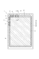
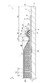
まず、図1及び図2を参照して本実施形態に係る放射線検出器1の構成について説明する。図1及び図2に示されるように、放射線検出器1は、光電変換素子アレイ7、シンチレータ層8、樹脂枠9、保護膜13、及び被覆樹脂層14を備えている。光電変換素子アレイ7は、基板2、受光部3、信号線4、ボンディングパッド5、及びパッシベーション膜6を有している。保護膜13は、第1の有機膜10、無機膜(金属膜)11、及び第2の有機膜12を有している。
First, the configuration of the radiation detector 1 according to the present embodiment will be described with reference to FIGS. 1 and 2. As shown in FIGS. 1 and 2, the radiation detector 1 includes a photoelectric
受光部3は、絶縁性の基板2(例えばガラス製基板)の中央部の矩形状領域に2次元に配列された複数の光電変換素子3aを含んで構成されている。光電変換素子3aは、アモルファスシリコン製のフォトダイオード(PD)や薄膜トランジスタ(TFT)等により構成されている。受光部3における各行又は各列の光電変換素子3aの各々は、信号読み出し用の信号線4により、外部回路(不図示)へ信号を取り出すためのボンディングパッド5と電気的に接続されている。
The
ボンディングパッド5は、基板2の外縁のうち隣接する2辺(図1における上辺、右辺)に沿って所定間隔毎に複数配置されており、信号線4を介して対応する複数の光電変換素子3aに電気的に接続されている。光電変換素子3a及び信号線4上には、絶縁性のパッシベーション膜6が形成されている。このパッシベーション膜6には、例えば窒化シリコンや酸化シリコン等を用いることができる。ボンディングパッド5は、外部回路との接続のために露出されている。
A plurality of
X線(放射線)を光に変換する柱状構造のシンチレータ8aが、受光部3を覆うように光電変換素子アレイ7上に積層されている。光電変換素子アレイ7における受光部3を含む略矩形状の領域(図1の破線で囲まれた領域)にシンチレータ8aが複数積層されることで、シンチレータ層8が形成されている。シンチレータ8aには、各種の材料を用いることができるが、例えば発光効率が良いTlドープのCsIを用いることができる。
A
シンチレータ層8の周縁部8bは、シンチレータ層8の外側に向かうにつれて高さが徐々に低くなるテーパ形状となっている。つまり、周縁部8bにおいて、シンチレータ層8の外側に形成されたシンチレータ8aほど、高さが低くなっている。ここで、周縁部8bは、下方に受光部3が形成されていない領域(有効画面外領域)、或いはX線画像生成における影響の小さい領域である。したがって、このようなテーパ形状の周縁部8bを設けることで、製造時においてレーザ光による悪影響が及ぶシンチレータ層8上の領域を限定することができる。ここで、周縁部8bの勾配角度、すなわち周縁部8bに形成されたシンチレータ8aの高さ位置をシンチレータ層8の内側から外側に向かって結んだ直線が基板2の上面に対してなす角度θは、20度〜80度の範囲に含まれる。
The
樹脂枠9は、シンチレータ層8の積層方向Aから見た場合に、シンチレータ層8とボンディングパッド5との間を通り且つシンチレータ層8を包囲するように、光電変換素子アレイ7上に形成されている。樹脂枠9の角部の形状は、外側に凸の弧状(いわゆるR形状)となっている。樹脂枠9は、例えばシリコン樹脂である。
The
樹脂枠9は、中央部が両縁部よりも高くなるように形成されており、樹脂枠9の高さd1は、シンチレータ層8の高さdよりも低くなっている。これにより、樹脂枠9を小型化すると共に、製造時におけるレーザ光によるシンチレータ層8への悪影響を抑制できる。ここで、樹脂枠9の高さd1は、光電変換素子アレイ7の上面位置と樹脂枠9の頂点位置との間の距離であり、シンチレータ層8の高さdは、シンチレータ層8に含まれるシンチレータ8aの最大の高さである。
The
樹脂枠9は、放射線検出器1を小型化する観点から、極力小さくすることが好ましい。より具体的には、樹脂枠9の高さd1は、450μm以下であり、樹脂枠9の幅d2は、900μm以下であることが好ましい。ここで、樹脂枠9の幅d2は、樹脂枠9の内縁E1(シンチレータ層8側の縁部)と樹脂枠9の外縁E2(ボンディングパッド5側の縁部)との間の幅である。
The
また、樹脂枠9の内縁E1とシンチレータ層8の外縁E3との間の距離(第1距離)D1は、樹脂枠9の外縁E2と光電変換素子アレイ7の外縁E4との間の距離(第2距離)D2よりも短くなっている。製造時におけるレーザ光によるボンディングパッド5への悪影響を抑制すると共に、シンチレータ層8の有効面積を確保するという観点から、第1距離D1に対する第2距離D2の比率は、5以上となっていることが好ましい。より具体的には、第1距離D1は、1mm以下であり、第2距離D2は、5mm以上であることが好ましい。これは、以下の理由による。
The distance (first distance) D1 between the inner edge E1 of the
シンチレータ層8の外縁E3と樹脂枠9の内縁E1との間に隙間がなければシンチレータ層8の有効面積を最大化できる。しかし、製造時におけるレーザ光によるシンチレータ層8への悪影響や、樹脂枠9を形成する工程でのわずかな失敗(例えば樹脂枠9をシンチレータ層8上に形成してしまうこと)のおそれを考慮すると、第1距離D1を1mm以下の範囲で確保することが好ましい。また、第2距離D2を5mm以上とすることで、製造時におけるレーザ光によるボンディングパッド5への悪影響を考慮して、樹脂枠9とボンディングパッド5との間に十分な距離を確保できる。
If there is no gap between the outer edge E3 of the
シンチレータ層8は、保護膜13で覆われている。保護膜13は、第1の有機膜10、無機膜11、及び第2の有機膜12が、この順にシンチレータ層8側から積層されることによって形成されている。第1の有機膜10、無機膜11、及び第2の有機膜12は、いずれもX線(放射線)を透過し、水蒸気を遮断する性質を有している。具体的には、第1の有機膜10及び第2の有機膜12には、ポリパラキシリレン樹脂、ポリパラクロロキシリレン等を用いることができる。また、無機膜11は、光に対しては、透明、不透明、反射性のいずれであってもよく、無機膜11には、例えばSi、Ti、Cr等の酸化膜、金、銀、アルミ(Al)等の金属膜を用いることができる。無機膜11として、光を反射させる金属膜を用いることで、シンチレータ8aで発生した蛍光が外に漏れるのを防ぐことができ、放射線検出器1の検出感度を向上させることができる。本実施形態では、無機膜11として成形が容易なAlを用いた例について説明する。Al自体は空気中で腐蝕しやすいが、無機膜11は、第1の有機膜10及び第2の有機膜12で挟まれているため、腐蝕から守られている。
The
保護膜13は、例えばCVD法によって形成される。このため、保護膜13を形成した直後の状態では、保護膜13は、光電変換素子アレイ7の表面全体を覆うように形成されている。そのため、ボンディングパッド5を露出させるために、保護膜13は、光電変換素子アレイ7のボンディングパッド5よりも内側の位置で切断され、外側の保護膜13は、除去される。後述するように、保護膜13は、樹脂枠9の中央部付近でレーザ光により切断(加工)され、保護膜13の外縁13aは、樹脂枠9によって固定される。これにより、保護膜13が外縁13aから剥がれるのを防止することができる。ここで、保護膜13の切断には、例えば炭酸ガスレーザ(CO2レーザ)や超短パルス(ナノ秒やピコ秒)の半導体レーザ等を用いることができる。炭酸ガスレーザを用いることで、一度の走査(短時間)で保護膜13の切断が可能となり、生産性が向上する。なお、光電変換素子アレイ7、ボンディングパッド5、及びシンチレータ層8等への悪影響とは、例えば炭酸ガスレーザや超短パルスレーザを用いる場合には、熱的なダメージである。
The
保護膜13の外縁13aは、樹脂枠9上に位置しており、樹脂枠9に沿って配置された被覆樹脂層14によって樹脂枠9と共にコーティングされている。被覆樹脂層14には、保護膜13及び樹脂枠9への接着性が良好な樹脂、例えばアクリル系接着剤等を用いることができる。なお、被覆樹脂層14には、樹脂枠9と同じシリコン樹脂を用いてもよい。或いは、樹脂枠9に被覆樹脂層14と同じアクリル系接着剤を用いてもよい。
An
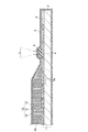
次に、図3を参照して、樹脂枠9及び保護膜13の角部(コーナー部分)について説明する。図3においては、樹脂枠9及び保護膜13の角部の状態を理解し易いように、被覆樹脂層14の図示を一部省略している。
Next, the corners (corner portions) of the
詳しくは後述するが、放射線検出器1の製造工程においてレーザ光が樹脂枠9上の保護膜13に照射されることで、保護膜13のレーザ光が照射された部分が、切断除去されている。ここで、保護膜13は、非常に薄いため、炭酸ガスレーザのレーザ光により、樹脂枠9の一部も併せて切断除去されている。これにより、樹脂枠9の中央付近には、溝部(対応領域)9aが形成されている。保護膜13の外縁13a、及び、樹脂枠9において保護膜13の外縁13aに対応する溝部9aは、レーザ光によって加工された状態となっている。ここで、溝部9aの深さ(高さ)d3は、樹脂枠9の高さd1の1/3以下とされている。これにより、樹脂枠9の下方に位置する光電変換素子アレイ7に対するレーザ光による悪影響が抑制されている。
As will be described in detail later, a portion of the
図3に示されるように、レーザ光によって加工された保護膜13の外縁13a及び溝部9aは、シンチレータ層8の積層方向Aから見た場合に、外側に凸の弧状の角部(図3に示す領域B参照)を有する略矩形環状に形成されている。また、保護膜13の外縁13a及び溝部9aは、積層方向Aから見た場合に、微細な波形状となっている。つまり、保護膜13の外縁13a及び溝部9aの表面は、例えばカッター等の刃物による平坦な切断面とは異なり、微小な凹凸形状を有するものとなっている。これにより、保護膜13の外縁13a及び溝部9aと被覆樹脂層14との接触面積が増えるため、保護膜13の外縁13a及び溝部9aと被覆樹脂層14との接着をより強固にすることができる。
As shown in FIG. 3, the
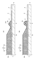
次に、図4〜図8を参照して、本実施形態に係る放射線検出器1の製造方法について説明する。まず、図4(a)に示されるように、光電変換素子アレイ7を準備する。続いて、図4(b)に示されるように、受光部3を覆う光電変換素子アレイ7上の領域において、TlをドープしたCsIの柱状結晶を例えば蒸着法により600μm程度の厚さに成長させることで、シンチレータ層8を形成(積層)する。
Next, with reference to FIGS. 4-8, the manufacturing method of the radiation detector 1 which concerns on this embodiment is demonstrated. First, as shown in FIG. 4A, a photoelectric
また、図5(a)に示されるように、樹脂枠9を、光電変換素子アレイ7上に形成する。具体的には、シンチレータ層8の積層方向Aから見た場合に、シンチレータ層8とボンディングパッド5との間を通り且つシンチレータ層8を包囲するように、樹脂枠9を形成する。より具体的には、第1距離D1が1mm以下となり、第2距離D2が5mm以上となるような位置に、樹脂枠9を形成する。樹脂枠9の形成には、例えば自動X−Yコーティング装置を用いることができる。以下、説明の便宜上、光電変換素子アレイ7上にシンチレータ層8及び樹脂枠9が形成されたものを指して、単に「基板」という。
In addition, as shown in FIG. 5A, the
シンチレータ層8を形成するCsIは、吸湿性が高く、露出したままにしておくと空気中の水蒸気を吸湿して溶解してしまう。そこで、例えばCVD法によって、基板全体の表面を、厚さ5〜25μmのポリパラキシリレンで被覆する。これにより、図5(b)に示されるように、第1の有機膜10が形成される。
CsI forming the
続いて、図6(a)に示されるように、放射線が入射する入射面(放射線検出器1のシンチレータ層8が形成される側の面)側の第1の有機膜10の表面に、0.2μm厚さのAl膜を蒸着法により積層することによって、無機膜(金属膜)11を形成する。続いて、無機膜11が形成された基板全体の表面を、再度CVD法によって、厚さ5〜25μmのポリパラキシリレンで被覆する。これにより、図6(b)に示されるように、第2の有機膜12が形成される。第2の有機膜12には、無機膜11の腐蝕による劣化を防ぐ役割がある。以上の処理により、保護膜13が形成される。保護膜13の樹脂枠9の略中央部分よりも外側の部分(ボンディングパッド5を覆う部分)は、後段の処理によって除去される。このため、光電変換素子アレイ7の側面及び光電変換素子アレイ7のシンチレータ層8が積層される側とは反対側の表面には、第1の有機膜10及び第2の有機膜12を形成しなくともよい。
Subsequently, as shown in FIG. 6A, 0 is formed on the surface of the first
続いて、図7に示されるように、樹脂枠9に沿って、レーザ光Lを照射し、保護膜13を切断する。具体的には、表面に保護膜13が形成された基板全体を載せたステージ(不図示)に対して、レーザ光Lを照射するレーザ光ヘッド(不図示)を移動させることで、レーザ光Lを樹脂枠9に沿って一筆書きの要領で走査する。より具体的には、樹脂枠9の略中央部分(最も厚みのある部分)に沿って、レーザ光Lを走査する。これにより、樹脂枠9の下方の光電変換素子アレイ7に対するレーザ光による悪影響を抑制できる。
Subsequently, as shown in FIG. 7, the
ここで、樹脂枠9の角部付近では、レーザ光Lの走査方向を切り替えるために走査速度を減速する必要がある。走査速度が減速された樹脂枠9上の位置においては、レーザ光の照射量が多くなるため溝部9aの深さが大きくなる。これにより、樹脂枠9の下方の光電変換素子アレイ7に対するレーザ光による悪影響が大きくなるという問題がある。しかし、本実施形態では、図3に示したように、保護膜13の外縁13a及び溝部9aが、角部において外側に凸の弧状(いわゆるR形状)となるように、レーザ光Lを走査させるので、角部におけるレーザ光Lの走査速度の減速度合を減らす、或いは、レーザ光Lの走査速度を減速せずに角部を加工することができる。これにより、樹脂枠9の角部付近において、樹脂枠9の下方の光電変換素子アレイ7に対するレーザ光による悪影響を抑制できる。
Here, in the vicinity of the corner of the
なお、樹脂枠9に沿って一筆書きの要領でレーザ光Lを走査する場合には、レーザ照射の開始位置と終了位置とで2重にレーザ照射がされる。このため、樹脂枠9の溝部9aの深さが大きくなり、樹脂枠9の下方の光電変換素子アレイ7に深刻な悪影響を与えてしまうおそれがある。しかし、本実施形態では、1回のレーザ光Lの照射により生じる溝部9aの深さd3が樹脂枠9の高さd1の1/3以下となるように、レーザ光Lの照射位置や照射強度等が制御される。これにより、同じ位置に2重にレーザ照射がされても、溝部9aの深さがそれほど大きくならず、樹脂枠9の下方の光電変換素子アレイ7に深刻な悪影響を与えてしまうことを防止できる。
In the case where the laser beam L is scanned along the
続いて、図8(a)に示されるように、保護膜13におけるレーザ光Lによる切断部から外側の部分(入射面と反対側の部分を含む)を除去することによって、ボンディングパッド5を露出させる。続いて、図8(b)に示されるように、樹脂枠9に沿って、保護膜13の外縁13a及び樹脂枠9を覆うように、紫外線硬化型のアクリル樹脂等の被覆樹脂をコーティングする。その後、紫外線照射によって、被覆樹脂を硬化させることで、被覆樹脂層14を形成する。
Subsequently, as shown in FIG. 8A, the
また、被覆樹脂層14を設けなくとも、保護膜13は、樹脂枠9を介して光電変換素子アレイ7に密着する。しかし、被覆樹脂層14を形成することによって、第1の有機膜10を含む保護膜13が樹脂枠9と被覆樹脂層14とに挟み込まれて固定され、光電変換素子アレイ7上への保護膜13の密着性がより一層向上する。したがって、保護膜13によりシンチレータ8aが密封されるので、シンチレータ8aへの水分の浸入を確実に防ぐことができ、シンチレータ8aの吸湿劣化による素子の解像度低下を防ぐことができる。
Even if the
次に、図1及び図2を参照して、本実施形態に係る放射線検出器1の動作について説明する。入射面側から入射したX線(放射線)は、保護膜13を透過してシンチレータ8aに達する。このX線は、シンチレータ8aによって吸収され、シンチレータ8aによってX線の光量に比例した光が放射される。放射された光のうち、X線の入射方向に逆行した光は、無機膜11で反射される。このため、シンチレータ8aで発生した光のほとんど全てが、パッシベーション膜6を介して光電変換素子3aに入射する。各々の光電変換素子3aは、光電変換により、入射した光の光量に対応する電気信号を生成し、一定時間蓄積する。この光の光量は、入射するX線の光量に対応している。つまり、各々の光電変換素子3aに蓄積される電気信号は、入射するX線の光量に対応することとなる。したがって、この電気信号によって、X線画像に対応する画像信号が得られる。光電変換素子3aに蓄積された画像信号は、信号線4を介してボンディングパッド5から順次読み出されて外部に転送される。転送された画像信号は、所定の処理回路で処理されることによって、X線画像が表示される。
Next, with reference to FIG.1 and FIG.2, operation | movement of the radiation detector 1 which concerns on this embodiment is demonstrated. X-rays (radiation) incident from the incident surface side pass through the
以上述べた放射線検出器1では、樹脂枠9上の保護膜13は、レーザ光により切断(加工)される。レーザ光による加工には、カッターによる切断と比較して熟練の技術が必要とされないので、生産性を向上することができる。また、レーザ光によれば、手作業による場合よりも精度良く保護膜13を切断することが可能であるため、樹脂枠9を小型化することができる。また、樹脂枠9は、シンチレータ層8及びボンディングパッド5から離間して形成されているので、製造時におけるレーザ光によるシンチレータ層8及びボンディングパッド5への悪影響を抑えることができる。一方で、樹脂枠9をシンチレータ層8に極力近づけて配置することで、シンチレータ層8の有効面積の大型化も図られている。したがって、放射線検出器1によれば、装置(放射線検出器1を含む放射線検出装置)の小型化及びシンチレータ層8の有効面積の大型化を両立すると共に、生産性の向上を図ることができる。
In the radiation detector 1 described above, the
また、本実施形態に係る放射線検出器1の製造方法によれば、レーザ光によって樹脂枠9上の保護膜13を切断するので、カッターによる切断と比較して熟練の技術が必要とされず、生産性を向上することができる。また、レーザ光によって、精度良く保護膜13を切断することが可能であるため、樹脂枠9を小型化することができる。また、樹脂枠9を、シンチレータ層8及びボンディングパッド5から離間して形成することで、保護膜13切断時におけるレーザ光によるシンチレータ層8及びボンディングパッド5への悪影響を抑えることができる。一方で、樹脂枠9をシンチレータ層8に近づけて形成することで、シンチレータ層8の有効面積の大型化も図られる。
Further, according to the method for manufacturing the radiation detector 1 according to the present embodiment, the
以上、本発明をその実施形態に基づいて詳細に説明した。しかし、本発明は上記実施形態に限定されるものではない。本発明は、その要旨を逸脱しない範囲において様々な変形が可能である。例えば、以上の説明では、保護膜13としてポリパラキシリレン製の有機膜10、12の間に無機膜11を挟み込んだ構造のものについて説明したが、第1の有機膜10と第2の有機膜12の材料は異なるものでも良い。また、無機膜11として腐蝕に強い材料を使用しているような場合は、第2の有機膜12自体を設けなくてもよい。また、受光部3として複数の光電変換素子3aが2次元に配列されたものについて説明したが、受光部3は、複数の光電変換素子3aが1次元に配列されたものであってもよい。そして、ボンディングパッド5は、矩形状の放射線検出器1の2辺でなく3辺に形成される場合もある。なお、上記実施形態においては、レーザ光ヘッドを移動させてレーザ加工する方法について説明したが、放射線検出器1を載置するステージを移動させて樹脂枠9及び保護膜13をレーザ加工してもよい。
The present invention has been described in detail based on the embodiments. However, the present invention is not limited to the above embodiment. The present invention can be variously modified without departing from the gist thereof. For example, in the above description, the
1…放射線検出器、2…基板、3…受光部、3a…光電変換素子、4…信号線、5…ボンディングパッド、6…パッシベーション膜、7…光電変換素子アレイ、8…シンチレータ層、8a…シンチレータ、8b…周縁部、9…樹脂枠、9a…溝部(対応領域)、10…第1の有機膜、11…無機膜(金属膜)、12…第2の有機膜、13…保護膜、13a…保護膜13の外縁、14…被覆樹脂層、D1…第1距離、D2…第2距離、d,d1,d3…高さ、d2…幅、E1…樹脂枠9の内縁、E2…樹脂枠9の外縁、E3…シンチレータ層8の外縁、E4…光電変換素子アレイ7の外縁。
DESCRIPTION OF SYMBOLS 1 ... Radiation detector, 2 ... Board | substrate, 3 ... Light-receiving part, 3a ... Photoelectric conversion element, 4 ... Signal line, 5 ... Bonding pad, 6 ... Passivation film, 7 ... Photoelectric conversion element array, 8 ... Scintillator layer, 8a ... Scintillator, 8b ... peripheral edge, 9 ... resin frame, 9a ... groove (corresponding region), 10 ... first organic film, 11 ... inorganic film (metal film), 12 ... second organic film, 13 ... protective film, 13a: outer edge of
Claims (11)
前記受光部を覆うように前記光電変換素子アレイ上に積層され、放射線を光に変換するシンチレータ層と、
前記シンチレータ層の積層方向から見た場合に、前記シンチレータ層及び前記ボンディングパッドから離間して前記シンチレータ層と前記ボンディングパッドとの間を通り且つ前記シンチレータ層を包囲するように、前記光電変換素子アレイ上に形成された樹脂枠と、
前記シンチレータ層を覆い、前記樹脂枠上に位置する外縁を有する保護膜と、を備え、
前記樹脂枠の内縁と前記シンチレータ層の外縁との間の第1距離は、前記樹脂枠の外縁と前記光電変換素子アレイの外縁との間の第2距離よりも短くなっており、
前記保護膜の前記外縁、及び前記樹脂枠において前記保護膜の前記外縁に対応する対応領域は、レーザ光によって加工された状態となっている、
放射線検出器。 A light receiving unit including a plurality of photoelectric conversion elements arranged one-dimensionally or two-dimensionally, and a photoelectric conversion element array having a plurality of bonding pads electrically connected to the photoelectric conversion elements and disposed outside the light receiving unit When,
A scintillator layer that is stacked on the photoelectric conversion element array so as to cover the light receiving unit and converts radiation into light;
The photoelectric conversion element array so as to pass between the scintillator layer and the bonding pad and surround the scintillator layer when viewed from the stacking direction of the scintillator layer. A resin frame formed on the top;
A protective film covering the scintillator layer and having an outer edge located on the resin frame,
The first distance between the inner edge of the resin frame and the outer edge of the scintillator layer is shorter than the second distance between the outer edge of the resin frame and the outer edge of the photoelectric conversion element array,
The outer edge of the protective film and the corresponding region corresponding to the outer edge of the protective film in the resin frame are processed by laser light.
Radiation detector.
請求項1記載の放射線検出器。 The outer edge and the corresponding region of the protective film have a fine wave shape when viewed from the stacking direction,
The radiation detector according to claim 1.
請求項1又は2記載の放射線検出器。 The height of the corresponding region is 1/3 or less of the height of the resin frame,
The radiation detector according to claim 1 or 2.
請求項1〜3のいずれか一項記載の放射線検出器。 The ratio of the second distance to the first distance is 5 or more.
The radiation detector as described in any one of Claims 1-3.
請求項1〜4のいずれか一項記載の放射線検出器。 The resin frame is formed such that the center portion is higher than both edge portions, and the height of the resin frame is lower than the height of the scintillator layer.
The radiation detector as described in any one of Claims 1-4.
前記樹脂枠の高さは、450μm以下である、
請求項5記載の放射線検出器。 The width between the inner edge of the resin frame and the outer edge of the resin frame is 900 μm or less,
The height of the resin frame is 450 μm or less,
The radiation detector according to claim 5.
請求項1〜6のいずれか一項記載の放射線検出器。 The outer edge and the corresponding region of the protective film processed by the laser beam are formed in a substantially rectangular ring shape having arc-shaped corner portions that protrude outward when viewed from the stacking direction.
The radiation detector as described in any one of Claims 1-6.
請求項1〜7のいずれか一項記載の放射線検出器。 A coating resin layer disposed along the resin frame so as to cover the outer edge of the protective film;
The radiation detector as described in any one of Claims 1-7.
請求項1〜8のいずれか一項記載の放射線検出器。 The peripheral portion of the scintillator layer has a tapered shape whose height gradually decreases toward the outside of the scintillator layer.
The radiation detector as described in any one of Claims 1-8.
請求項1〜9のいずれか一項記載の放射線検出器。 The protective film includes a metal film that reflects light,
The radiation detector as described in any one of Claims 1-9.
前記シンチレータ層の積層方向から見た場合に、前記シンチレータ層及び前記ボンディングパッドから離間して前記シンチレータ層と前記ボンディングパッドとの間を通り且つ前記シンチレータ層を包囲するように、前記光電変換素子アレイ上に樹脂枠を形成する工程と、
少なくとも前記光電変換素子アレイの前記シンチレータ層が積層される側の表面全体を覆うように保護膜を形成する工程と、
前記樹脂枠に沿ってレーザ光を照射することで、前記保護膜を切断し、前記保護膜の外側の部分を除去する工程と、を有し、
前記樹脂枠を形成する工程では、前記樹脂枠の内縁と前記シンチレータ層の外縁との間の第1距離が、前記樹脂枠の外縁と前記光電変換素子アレイの外縁との間の第2距離よりも短くなるように、前記樹脂枠を形成する、
放射線検出器の製造方法。 A light receiving unit including a plurality of photoelectric conversion elements arranged one-dimensionally or two-dimensionally, and a photoelectric conversion element array having a plurality of bonding pads electrically connected to the photoelectric conversion elements and disposed outside the light receiving unit A step of laminating a scintillator layer for converting radiation into light on the photoelectric conversion element array so as to cover the light receiving portion;
The photoelectric conversion element array so as to pass between the scintillator layer and the bonding pad and surround the scintillator layer when viewed from the stacking direction of the scintillator layer. Forming a resin frame thereon;
Forming a protective film so as to cover at least the entire surface of the photoelectric conversion element array on the side where the scintillator layer is laminated;
Irradiating a laser beam along the resin frame to cut the protective film and removing a portion outside the protective film, and
In the step of forming the resin frame, the first distance between the inner edge of the resin frame and the outer edge of the scintillator layer is greater than the second distance between the outer edge of the resin frame and the outer edge of the photoelectric conversion element array. Forming the resin frame so as to be shorter,
A method for manufacturing a radiation detector.
Priority Applications (11)
| Application Number | Priority Date | Filing Date | Title |
|---|---|---|---|
| JP2013236693A JP2015096823A (en) | 2013-11-15 | 2013-11-15 | Radiation detector and radiation detector manufacturing method |
| EP14861967.9A EP3070499B1 (en) | 2013-11-15 | 2014-10-10 | Radiation detector, and method for producing radiation detector |
| KR1020207037144A KR20210000738A (en) | 2013-11-15 | 2014-10-10 | Radiation detector, and method for producing radiation detector |
| PCT/JP2014/077252 WO2015072260A1 (en) | 2013-11-15 | 2014-10-10 | Radiation detector, and method for producing radiation detector |
| CN201910655336.4A CN110361771A (en) | 2013-11-15 | 2014-10-10 | The manufacturing method of radiation detector and radiation detector |
| CN201480061928.9A CN105723244B (en) | 2013-11-15 | 2014-10-10 | The manufacturing method of radiation detector and radiation detector |
| US15/030,412 US10061035B2 (en) | 2013-11-15 | 2014-10-10 | Radiation detector, and method for producing radiation detector |
| KR1020167015409A KR20160085840A (en) | 2013-11-15 | 2014-10-10 | Radiation detector, and method for producing radiation detector |
| US15/982,705 US10514470B2 (en) | 2013-11-15 | 2018-05-17 | Radiation detector, and method for producing radiation detector |
| US15/982,771 US10571581B2 (en) | 2013-11-15 | 2018-05-17 | Radiation detector, and method for producing radiation detector |
| US16/729,726 US11506799B2 (en) | 2013-11-15 | 2019-12-30 | Radiation detector, and method for producing radiation detector |
Applications Claiming Priority (1)
| Application Number | Priority Date | Filing Date | Title |
|---|---|---|---|
| JP2013236693A JP2015096823A (en) | 2013-11-15 | 2013-11-15 | Radiation detector and radiation detector manufacturing method |
Related Child Applications (1)
| Application Number | Title | Priority Date | Filing Date |
|---|---|---|---|
| JP2018011783A Division JP6535769B2 (en) | 2018-01-26 | 2018-01-26 | Method of manufacturing radiation detector |
Publications (2)
| Publication Number | Publication Date |
|---|---|
| JP2015096823A true JP2015096823A (en) | 2015-05-21 |
| JP2015096823A5 JP2015096823A5 (en) | 2016-09-08 |
Family
ID=53057202
Family Applications (1)
| Application Number | Title | Priority Date | Filing Date |
|---|---|---|---|
| JP2013236693A Pending JP2015096823A (en) | 2013-11-15 | 2013-11-15 | Radiation detector and radiation detector manufacturing method |
Country Status (6)
| Country | Link |
|---|---|
| US (4) | US10061035B2 (en) |
| EP (1) | EP3070499B1 (en) |
| JP (1) | JP2015096823A (en) |
| KR (2) | KR20160085840A (en) |
| CN (2) | CN110361771A (en) |
| WO (1) | WO2015072260A1 (en) |
Cited By (6)
| Publication number | Priority date | Publication date | Assignee | Title |
|---|---|---|---|---|
| WO2017171387A1 (en) * | 2016-03-31 | 2017-10-05 | 주식회사 아비즈알 | Scintillator panel and method for manufacturing same |
| JP2017187339A (en) * | 2016-04-04 | 2017-10-12 | 東芝電子管デバイス株式会社 | Radiation detector and method for manufacturing the same |
| KR20170134672A (en) * | 2015-06-10 | 2017-12-06 | 도시바 덴시칸 디바이스 가부시키가이샤 | Array substrate and radiation detector |
| JP2018179514A (en) * | 2017-04-03 | 2018-11-15 | 東芝電子管デバイス株式会社 | Radiation detector |
| WO2021131239A1 (en) | 2019-12-25 | 2021-07-01 | 浜松ホトニクス株式会社 | Radiation detector and method for manufacturing radiation detector |
| WO2021131236A1 (en) | 2019-12-25 | 2021-07-01 | 浜松ホトニクス株式会社 | Radiation detector and method for manufacturing radiation detector |
Families Citing this family (8)
| Publication number | Priority date | Publication date | Assignee | Title |
|---|---|---|---|---|
| JP2015096823A (en) | 2013-11-15 | 2015-05-21 | 浜松ホトニクス株式会社 | Radiation detector and radiation detector manufacturing method |
| JP6487263B2 (en) * | 2015-04-20 | 2019-03-20 | 浜松ホトニクス株式会社 | Radiation detector and manufacturing method thereof |
| JP6717126B2 (en) * | 2016-09-01 | 2020-07-01 | コニカミノルタ株式会社 | Radiation image detector |
| CN109964118A (en) * | 2016-11-10 | 2019-07-02 | 皇家飞利浦有限公司 | Phase contrast imaging based on grating |
| US10921467B2 (en) * | 2017-09-15 | 2021-02-16 | Analogic Corporation | Detector array for imaging modality |
| JP6433561B1 (en) * | 2017-09-27 | 2018-12-05 | 浜松ホトニクス株式会社 | Scintillator panel and radiation detector |
| CN109659385A (en) * | 2017-10-10 | 2019-04-19 | 群创光电股份有限公司 | Sensing device |
| CN110081904B (en) * | 2019-05-15 | 2021-01-29 | 合肥工业大学 | Attitude measuring device and method for double-plane photoelectric sensor array tube push bench |
Citations (5)
| Publication number | Priority date | Publication date | Assignee | Title |
|---|---|---|---|---|
| JP3077941B2 (en) * | 1997-02-14 | 2000-08-21 | 浜松ホトニクス株式会社 | Radiation detecting element and method of manufacturing the same |
| JP2006052981A (en) * | 2004-08-10 | 2006-02-23 | Canon Inc | Radiation detector, manufacturing method for the same and radiation detection system |
| JP2009260017A (en) * | 2008-04-16 | 2009-11-05 | Nec Tokin Corp | Method of manufacturing solid electrolytic capacitor |
| JP2010046757A (en) * | 2008-08-21 | 2010-03-04 | Sumitomo Electric Hardmetal Corp | Cutting tool and method of manufacturing the same |
| JP2012023335A (en) * | 2010-06-17 | 2012-02-02 | Sony Chemical & Information Device Corp | Thermally conductive sheet and method of producing the same |
Family Cites Families (38)
| Publication number | Priority date | Publication date | Assignee | Title |
|---|---|---|---|---|
| US61035A (en) * | 1867-01-08 | Louis knell | ||
| JPS60149944A (en) | 1984-01-17 | 1985-08-07 | Meidensha Electric Mfg Co Ltd | Chassis dynamotor |
| JPS6247167A (en) | 1985-08-27 | 1987-02-28 | Matsushita Electric Ind Co Ltd | Multi-channel semiconductor radiation detector |
| JP2883360B2 (en) | 1989-08-21 | 1999-04-19 | 富士写真フイルム株式会社 | Processing method of photosensitive material |
| US5229613A (en) * | 1991-09-06 | 1993-07-20 | Horiba Instruments, Incorporated | Extended lifetime scintillation camera plate assembly |
| JP3405706B2 (en) * | 1997-02-14 | 2003-05-12 | 浜松ホトニクス株式会社 | Radiation detection element |
| CA2261663C (en) * | 1997-02-14 | 2001-08-28 | Hamamatsu Photonics K.K. | Radiation detection device and method of producing the same |
| JP3029873B2 (en) | 1997-02-14 | 2000-04-10 | 浜松ホトニクス株式会社 | Radiation detecting element and method of manufacturing the same |
| JP4317154B2 (en) * | 1998-06-18 | 2009-08-19 | 浜松ホトニクス株式会社 | Scintillator panel and radiation image sensor |
| EP1118879B1 (en) * | 1998-06-18 | 2006-04-26 | Hamamatsu Photonics K.K. | Scintillator panel and radiation image sensor |
| US6407360B1 (en) | 1998-08-26 | 2002-06-18 | Samsung Electronics, Co., Ltd. | Laser cutting apparatus and method |
| KR100734546B1 (en) | 2000-01-13 | 2007-07-04 | 하마마츠 포토닉스 가부시키가이샤 | Radiation image sensor and scintillator panel |
| JP3833872B2 (en) * | 2000-04-26 | 2006-10-18 | 日本電産サンキョー株式会社 | Optical pickup device |
| JP3077941U (en) | 2000-11-27 | 2001-06-12 | 株式会社大廣 | Liquid combustible gasifier using carbide |
| JP2003066150A (en) | 2001-08-30 | 2003-03-05 | Canon Inc | Fluorescent plate, radiation detector and radiation detecting system |
| JP2004264239A (en) | 2003-03-04 | 2004-09-24 | Canon Inc | Radiographing device |
| JP2004317167A (en) * | 2003-04-11 | 2004-11-11 | Canon Inc | Radiation detection apparatus |
| US7193218B2 (en) * | 2003-10-29 | 2007-03-20 | Canon Kabushiki Kaisha | Radiation detection device, method of producing the same, and radiation image pick-up system |
| JP2005144973A (en) | 2003-11-19 | 2005-06-09 | Process Lab Micron:Kk | Perforated printing mask |
| JP4335025B2 (en) | 2004-01-29 | 2009-09-30 | 浜松ホトニクス株式会社 | Radiation image sensor and manufacturing method thereof |
| JP2006052985A (en) | 2004-08-10 | 2006-02-23 | Canon Inc | Method of manufacturing radiation detector and radiation detecting system |
| JP4266898B2 (en) | 2004-08-10 | 2009-05-20 | キヤノン株式会社 | Radiation detection apparatus, manufacturing method thereof, and radiation imaging system |
| US7828926B1 (en) | 2006-04-04 | 2010-11-09 | Radiation Monitoring Devices, Inc. | Selective removal of resin coatings and related methods |
| JP4764407B2 (en) * | 2007-11-20 | 2011-09-07 | 東芝電子管デバイス株式会社 | Radiation detector and manufacturing method thereof |
| WO2010010725A1 (en) | 2008-07-25 | 2010-01-28 | コニカミノルタエムジー株式会社 | Scintillator panel and radiographic image detector provided with the same |
| JP2010118602A (en) | 2008-11-14 | 2010-05-27 | Hamamatsu Photonics Kk | Method of manufacturing radiation detector |
| JP2010204072A (en) | 2009-03-06 | 2010-09-16 | Konica Minolta Medical & Graphic Inc | Panel and device for detection of radiation image |
| JP2011174830A (en) * | 2010-02-25 | 2011-09-08 | Konica Minolta Medical & Graphic Inc | Radiation detection panel and radiation image detector |
| KR20110113482A (en) | 2010-04-09 | 2011-10-17 | (주)비엠알테크놀러지 | Manufacturing method of x-ray image sensor by direct deposition |
| JP2012004394A (en) | 2010-06-18 | 2012-01-05 | Konica Minolta Medical & Graphic Inc | Radiation image pickup device |
| JP2012185123A (en) | 2011-03-08 | 2012-09-27 | Sony Corp | Radiographic apparatus and manufacturing method for radiographic apparatuses |
| JP5498982B2 (en) | 2011-03-11 | 2014-05-21 | 富士フイルム株式会社 | Radiography equipment |
| KR101266554B1 (en) * | 2011-05-09 | 2013-05-27 | 주식회사 아비즈알 | A scintillator panel and a method for manufacturing the sintillator panel |
| GB2492972B (en) * | 2011-07-15 | 2013-09-11 | M Solv Ltd | Method and apparatus for dividing a thin film device into separate cells |
| KR101925895B1 (en) * | 2011-12-29 | 2018-12-07 | 삼성디스플레이 주식회사 | The panel for detecting x-ray and method of making the same |
| JP6071283B2 (en) * | 2012-07-04 | 2017-02-01 | キヤノン株式会社 | Radiation detection apparatus and manufacturing method thereof |
| JP6100045B2 (en) * | 2013-03-19 | 2017-03-22 | キヤノン株式会社 | Radiation detection apparatus, radiation detection system, and method of manufacturing radiation detection apparatus |
| JP2015096823A (en) * | 2013-11-15 | 2015-05-21 | 浜松ホトニクス株式会社 | Radiation detector and radiation detector manufacturing method |
-
2013
- 2013-11-15 JP JP2013236693A patent/JP2015096823A/en active Pending
-
2014
- 2014-10-10 KR KR1020167015409A patent/KR20160085840A/en not_active Application Discontinuation
- 2014-10-10 KR KR1020207037144A patent/KR20210000738A/en not_active Application Discontinuation
- 2014-10-10 EP EP14861967.9A patent/EP3070499B1/en active Active
- 2014-10-10 US US15/030,412 patent/US10061035B2/en active Active
- 2014-10-10 CN CN201910655336.4A patent/CN110361771A/en active Pending
- 2014-10-10 WO PCT/JP2014/077252 patent/WO2015072260A1/en active Application Filing
- 2014-10-10 CN CN201480061928.9A patent/CN105723244B/en active Active
-
2018
- 2018-05-17 US US15/982,705 patent/US10514470B2/en active Active
- 2018-05-17 US US15/982,771 patent/US10571581B2/en active Active
-
2019
- 2019-12-30 US US16/729,726 patent/US11506799B2/en active Active
Patent Citations (5)
| Publication number | Priority date | Publication date | Assignee | Title |
|---|---|---|---|---|
| JP3077941B2 (en) * | 1997-02-14 | 2000-08-21 | 浜松ホトニクス株式会社 | Radiation detecting element and method of manufacturing the same |
| JP2006052981A (en) * | 2004-08-10 | 2006-02-23 | Canon Inc | Radiation detector, manufacturing method for the same and radiation detection system |
| JP2009260017A (en) * | 2008-04-16 | 2009-11-05 | Nec Tokin Corp | Method of manufacturing solid electrolytic capacitor |
| JP2010046757A (en) * | 2008-08-21 | 2010-03-04 | Sumitomo Electric Hardmetal Corp | Cutting tool and method of manufacturing the same |
| JP2012023335A (en) * | 2010-06-17 | 2012-02-02 | Sony Chemical & Information Device Corp | Thermally conductive sheet and method of producing the same |
Cited By (13)
| Publication number | Priority date | Publication date | Assignee | Title |
|---|---|---|---|---|
| KR20170134672A (en) * | 2015-06-10 | 2017-12-06 | 도시바 덴시칸 디바이스 가부시키가이샤 | Array substrate and radiation detector |
| EP3309591A4 (en) * | 2015-06-10 | 2019-03-20 | Canon Electron Tubes & Devices Co., Ltd. | Array substrate and radiation detector |
| KR102001168B1 (en) | 2015-06-10 | 2019-07-17 | 캐논 덴시칸 디바이스 가부시키가이샤 | Array substrate and radiation detector |
| WO2017171387A1 (en) * | 2016-03-31 | 2017-10-05 | 주식회사 아비즈알 | Scintillator panel and method for manufacturing same |
| JP2017187339A (en) * | 2016-04-04 | 2017-10-12 | 東芝電子管デバイス株式会社 | Radiation detector and method for manufacturing the same |
| JP2018179514A (en) * | 2017-04-03 | 2018-11-15 | 東芝電子管デバイス株式会社 | Radiation detector |
| WO2021131239A1 (en) | 2019-12-25 | 2021-07-01 | 浜松ホトニクス株式会社 | Radiation detector and method for manufacturing radiation detector |
| WO2021131236A1 (en) | 2019-12-25 | 2021-07-01 | 浜松ホトニクス株式会社 | Radiation detector and method for manufacturing radiation detector |
| KR20220118395A (en) | 2019-12-25 | 2022-08-25 | 하마마츠 포토닉스 가부시키가이샤 | Radiation detector and manufacturing method of radiation detector |
| KR20220118394A (en) | 2019-12-25 | 2022-08-25 | 하마마츠 포토닉스 가부시키가이샤 | Radiation detector and manufacturing method of radiation detector |
| US11644581B2 (en) | 2019-12-25 | 2023-05-09 | Hamamatsu Photonics K.K. | Radiation detector and method for manufacturing radiation detector |
| JP7345385B2 (en) | 2019-12-25 | 2023-09-15 | 浜松ホトニクス株式会社 | Radiation detector and radiation detector manufacturing method |
| US11762110B2 (en) | 2019-12-25 | 2023-09-19 | Hamamatsu Photonics K.K. | Radiation detector and method for manufacturing radiation detector |
Also Published As
| Publication number | Publication date |
|---|---|
| US20180267179A1 (en) | 2018-09-20 |
| US10061035B2 (en) | 2018-08-28 |
| EP3070499B1 (en) | 2019-05-22 |
| CN110361771A (en) | 2019-10-22 |
| US11506799B2 (en) | 2022-11-22 |
| US10514470B2 (en) | 2019-12-24 |
| US20180267178A1 (en) | 2018-09-20 |
| US20200142082A1 (en) | 2020-05-07 |
| KR20210000738A (en) | 2021-01-05 |
| CN105723244A (en) | 2016-06-29 |
| WO2015072260A1 (en) | 2015-05-21 |
| KR20160085840A (en) | 2016-07-18 |
| EP3070499A4 (en) | 2017-07-12 |
| EP3070499A1 (en) | 2016-09-21 |
| CN105723244B (en) | 2019-08-20 |
| US10571581B2 (en) | 2020-02-25 |
| US20160245931A1 (en) | 2016-08-25 |
Similar Documents
| Publication | Publication Date | Title |
|---|---|---|
| US11506799B2 (en) | Radiation detector, and method for producing radiation detector | |
| US10379229B2 (en) | Radiation detector and method for producing same | |
| US20140008749A1 (en) | Radiation detection apparatus and method of manufacturing the same | |
| JP2019164163A (en) | Radiation detector | |
| JP6535769B2 (en) | Method of manufacturing radiation detector | |
| JP2020177033A (en) | Radiation detector | |
| JP7345385B2 (en) | Radiation detector and radiation detector manufacturing method | |
| US11762110B2 (en) | Radiation detector and method for manufacturing radiation detector | |
| JP2011027469A (en) | X-ray detector |
Legal Events
| Date | Code | Title | Description |
|---|---|---|---|
| A521 | Request for written amendment filed |
Free format text: JAPANESE INTERMEDIATE CODE: A523 Effective date: 20160720 |
|
| A621 | Written request for application examination |
Free format text: JAPANESE INTERMEDIATE CODE: A621 Effective date: 20160720 |
|
| A131 | Notification of reasons for refusal |
Free format text: JAPANESE INTERMEDIATE CODE: A131 Effective date: 20170509 |
|
| A521 | Request for written amendment filed |
Free format text: JAPANESE INTERMEDIATE CODE: A523 Effective date: 20170622 |
|
| A02 | Decision of refusal |
Free format text: JAPANESE INTERMEDIATE CODE: A02 Effective date: 20171114 |
|
| A521 | Request for written amendment filed |
Free format text: JAPANESE INTERMEDIATE CODE: A523 Effective date: 20180126 |
|
| A911 | Transfer to examiner for re-examination before appeal (zenchi) |
Free format text: JAPANESE INTERMEDIATE CODE: A911 Effective date: 20180206 |
|
| A912 | Re-examination (zenchi) completed and case transferred to appeal board |
Free format text: JAPANESE INTERMEDIATE CODE: A912 Effective date: 20180309 |
|
| A521 | Request for written amendment filed |
Free format text: JAPANESE INTERMEDIATE CODE: A523 Effective date: 20181114 |