CN102064698B - Information device - Google Patents
Information device Download PDFInfo
- Publication number
- CN102064698B CN102064698B CN2010105487858A CN201010548785A CN102064698B CN 102064698 B CN102064698 B CN 102064698B CN 2010105487858 A CN2010105487858 A CN 2010105487858A CN 201010548785 A CN201010548785 A CN 201010548785A CN 102064698 B CN102064698 B CN 102064698B
- Authority
- CN
- China
- Prior art keywords
- circuit
- signal
- switch
- latch
- pattern
- Prior art date
- Legal status (The legal status is an assumption and is not a legal conclusion. Google has not performed a legal analysis and makes no representation as to the accuracy of the status listed.)
- Active
Links
Images


Classifications
-
- G—PHYSICS
- G06—COMPUTING; CALCULATING OR COUNTING
- G06F—ELECTRIC DIGITAL DATA PROCESSING
- G06F1/00—Details not covered by groups G06F3/00 - G06F13/00 and G06F21/00
- G06F1/26—Power supply means, e.g. regulation thereof
- G06F1/32—Means for saving power
- G06F1/3203—Power management, i.e. event-based initiation of a power-saving mode
-
- G—PHYSICS
- G06—COMPUTING; CALCULATING OR COUNTING
- G06F—ELECTRIC DIGITAL DATA PROCESSING
- G06F1/00—Details not covered by groups G06F3/00 - G06F13/00 and G06F21/00
- G06F1/26—Power supply means, e.g. regulation thereof
-
- G—PHYSICS
- G06—COMPUTING; CALCULATING OR COUNTING
- G06F—ELECTRIC DIGITAL DATA PROCESSING
- G06F1/00—Details not covered by groups G06F3/00 - G06F13/00 and G06F21/00
- G06F1/26—Power supply means, e.g. regulation thereof
- G06F1/30—Means for acting in the event of power-supply failure or interruption, e.g. power-supply fluctuations
-
- G—PHYSICS
- G06—COMPUTING; CALCULATING OR COUNTING
- G06F—ELECTRIC DIGITAL DATA PROCESSING
- G06F3/00—Input arrangements for transferring data to be processed into a form capable of being handled by the computer; Output arrangements for transferring data from processing unit to output unit, e.g. interface arrangements
- G06F3/12—Digital output to print unit, e.g. line printer, chain printer
- G06F3/1201—Dedicated interfaces to print systems
- G06F3/1202—Dedicated interfaces to print systems specifically adapted to achieve a particular effect
- G06F3/1218—Reducing or saving of used resources, e.g. avoiding waste of consumables or improving usage of hardware resources
- G06F3/1221—Reducing or saving of used resources, e.g. avoiding waste of consumables or improving usage of hardware resources with regard to power consumption
-
- H—ELECTRICITY
- H01—ELECTRIC ELEMENTS
- H01H—ELECTRIC SWITCHES; RELAYS; SELECTORS; EMERGENCY PROTECTIVE DEVICES
- H01H47/00—Circuit arrangements not adapted to a particular application of the relay and designed to obtain desired operating characteristics or to provide energising current
-
- H—ELECTRICITY
- H02—GENERATION; CONVERSION OR DISTRIBUTION OF ELECTRIC POWER
- H02J—CIRCUIT ARRANGEMENTS OR SYSTEMS FOR SUPPLYING OR DISTRIBUTING ELECTRIC POWER; SYSTEMS FOR STORING ELECTRIC ENERGY
- H02J9/00—Circuit arrangements for emergency or stand-by power supply, e.g. for emergency lighting
- H02J9/005—Circuit arrangements for emergency or stand-by power supply, e.g. for emergency lighting using a power saving mode
- H02J9/007—Detection of the absence of a load
Abstract
The invention provides an information device. The compact information device in which a shortened unlatch time is enabled so such device can transition from a power cutoff mode to a power supply mode to resume supplying DC power to internal circuits as a result of a latch circuit unlatching a control signal. A printer includes a CPU, A tactile switch, A smoothing capacitor, A switch circuit, a switch control signal generator including a latch circuit, and a potential difference detection circuit. The latch circuit and potential difference detection circuit operate with voltage. The CPU outputs a start latch signal when the operating mode changes from the power supply mode to the power cutoff mode. When the tactile switch is turned off, the potential difference detection circuit outputs an unlatch signal. When the unlatch signal is input, the latch circuit unlatches the control signal.
Description
Technical field
The present invention relates to a kind of information equipment.
Background technology
In the so-called small information equipment such as printer, have and utilize the type of being moved from being connected in the direct current power that outside supply unit provides.And, in recent years, in order to suppress power consumption, require as follows information equipment: even mains switch is on-state, can't use for a long time information equipment, and do not provide in the situation of the function of tonic chord, cutting off the internal circuit that comprises CPU is the providing of direct current power at the many positions of the consumption of electric power.And then; for energy, using during product gives the ErP instruction (Directive on Eco-Design of Energy Related Products) of the obligation of Environment Protection Design, to require Disconnected mode be that equipment is connected with source power supply but the power consumption inhibition in the operate condition of any function is not provided is below 0.5 (W).
In possessing the information equipment of Disconnected mode, as providing the electric power of direct current power to supply with to internal circuit to cut off circuit for cutting off, comprise for cutting off to internal circuit and the switching circuit of direct current power is provided and latchs (lock) circuit for what this switching circuit is remained to open mode.In addition, in this information equipment, also possesses the discharge circuit that comprises discharge resistance for making the stable smmothing capacitor of supply voltage and discharging for the residual charge that makes as required this smmothing capacitor.In addition, as smmothing capacitor, use the larger capacitor of capacity ratio.
In such information equipment, cut off while to internal circuit, providing direct current power, for example, from CPU to latch cicuit input and latch commencing signal, latch cicuit is latched latching commencing signal.Then, latch cicuit, to during latching that commencing signal latched, should remain switching circuit the switch controlling signal of open mode to switching circuit output.During this switch controlling signal of input, latch cicuit is to during latching that commencing signal latched, and switching circuit stays open state, cuts off and provides direct current power to internal circuit.In addition, in order again to start from this state to the providing of the direct current power of internal circuit, turn back to on-state after the mains switch of information equipment temporarily need to being switched to off-state.Reason is as follows.
That is, at switching circuit, for open mode and cut off while to internal circuit, providing direct current power, if the mains switch of information equipment is switched to open mode, by discharge circuit, move, the residual charge of smmothing capacitor is discharged.Afterwards, if by the electric discharge of this residual charge, the lower voltage between two terminals of smmothing capacitor must be less than the operation voltage of latch cicuit, and the latching of commencing signal of latching in latch cicuit is disengaged (latching releasing).Latch releasing by this, switching circuit becomes closure state, when mains switch is switched to on-state again, to the internal circuit that comprises CPU, provides direct current power.
[patent documentation 1] TOHKEMY 2006-166561 communique
[patent documentation 2] TOHKEMY 2005-312162 communique
In addition, as mentioned above, the user of information equipment provides direct current power in order again to start to internal circuit sometimes, carries out mains switch is switched to the operation that off-state is returned to on-state afterwards immediately.In this case, the residual charge of smmothing capacitor is not discharged fully sometimes, and does not carry out the releasing of latching of latch cicuit.Now, even mains switch is switched to on-state, also because of switching circuit still in open mode, so can not provide direct current power to internal circuit, the internal circuit akinesia.In order to remove such unfavorable condition, consider following situation: the discharge resistance possessed as discharge circuit, use the resistor that resistance value is as far as possible little and permissible loss is large as far as possible, thereby shorten to latch, remove the required time (latching the releasing time).
But, because the resistor general appearance size with above-mentioned characteristic is larger, so such resistor can be caused to the maximization of information equipment as discharge resistance.Therefore, there is the resistor of above-mentioned characteristic and be not suitable for carrying in information equipment.
Summary of the invention
The present invention completes in order to solve above-mentioned problem, its purpose is, when cut-out provides direct current power to the internal circuit that comprises CPU, remove and again to start to provide in the information equipment of direct current power to internal circuit by latching of latch cicuit, can take into account the miniaturization of information equipment and latch the shortening of releasing time.
The present invention, at least a portion solved in above-mentioned problem completes, can be used as following mode or application examples and realizes.
[application examples 1]
A kind of information equipment, the control part that utilizes the direct current power from being connected to outside supply unit and providing to be moved is provided, and have as pattern: the first pattern of described direct current power is provided and cuts off the second pattern that described direct current power is provided to described control part to described control part, this information equipment comprises:
Mains switch, it has input terminal, lead-out terminal and operating portion, in described mains switch, described input terminal is connected with described supply unit, become the handover operation of the posture of the described operating portion of switching between the prime of on-state and second that described connection status becomes off state by the connection status at described input terminal and described lead-out terminal, switch described connection status, and only otherwise carry out described handover operation, keep posture and the described connection status of described operating portion;
Smmothing capacitor, it has the first terminal and the second terminal, and described the first terminal is connected with the described lead-out terminal of described mains switch, and described the second terminal is grounded;
Switching circuit, it is connected with the described lead-out terminal of described mains switch, and the providing and cutting off to the described direct current power of described control part for switching;
The switch controlling signal generative circuit, it has the latch cicuit that commencing signal is latched that latchs from described control part input, and the described latch mode that latchs commencing signal based in described latch cicuit at least, generation should be cut off the switch controlling signal that described direct current power is provided to described control part, and outputs to described switching circuit; And
Latch the ring off signal generating unit, it detects the described connection status in described mains switch, and in the situation that described connection status is off state, the described ring off signal of latching of latching of latching commencing signal that should remove in described latch cicuit outputs to described switch controlling signal generative circuit
Described latch cicuit and the described ring off signal generating unit that latchs are configured to and can utilize from the described lead-out terminal of described mains switch or the described direct current power that provides from described smmothing capacitor and be moved,
When described pattern is transferred to described the second pattern from described first mode, described control part outputs to described switch controlling signal generative circuit by the described commencing signal that latchs,
To described latch cicuit, input describedly while latching ring off signal, described latch cicuit is removed described the latching of commencing signal of latching,
When having inputted described switch controlling signal, described switching circuit becomes open mode,
When not inputting described switch controlling signal, described switching circuit becomes closure state.
Wherein, the input terminal of mains switch might not need directly to be connected with the first terminal of smmothing capacitor, lead-out terminal and the switching circuit of mains switch with the lead-out terminal of supply unit, mains switch, also can be between them other the circuit element such as contact resistance device.
In the information equipment of application examples 1, in the situation that pattern is that the second pattern and switching circuit are open mode, become following action.
1) posture of the operating portion of mains switch switches to second from prime, and the connection status of input terminal and lead-out terminal becomes off-state.
2) latch the ring off signal generating unit and detect the situation that mains switch switches to off-state, by latching ring off signal, output to the switch controlling signal generative circuit with latch cicuit.
3) latch cicuit is latched releasing having inputted while latching ring off signal.
Therefore, even the residual charge of smmothing capacitor is not discharged fully, and the voltage between two terminals of smmothing capacitor do not become and is less than the operation voltage of latch cicuit, and latch cicuit also can be latched releasing.Therefore, in should the information equipment of use-case, not need to for shorten latch the releasing time and will before explanation, resistor that resistance value is little and permissible loss is large as discharge resistance.That is, by should use-case, can take into account the miniaturization of information equipment and latch the shortening of releasing time.
In addition, in this manual, " input terminal of mains switch and the connection status between lead-out terminal are on-state " (also referred to as " mains switch is on-state ") refers to that at least the posture of the operating portion of mains switch is prime.In addition, " input terminal of mains switch and the connection status between lead-out terminal are off-state " (also referred to as " mains switch is off-state ") refers to that at least the posture of the operating portion of mains switch is second.
[application examples 2]
According to the described information equipment of application examples 1, wherein,
The described ring off signal generating unit that latchs comprises: the potential difference testing circuit, this potential difference testing circuit detects the described input terminal of described mains switch and the potential difference between described lead-out terminal, and in the situation that described potential difference is more than setting, the situation that is off state as described connection status, latch ring off signal and output to described switch controlling signal generative circuit described.
In the information equipment of application examples 2, become following action.
1) in the situation that pattern is the second pattern and switching circuit is open mode, the posture of the operating portion of described mains switch switches to second from prime, and the connection status between input terminal and lead-out terminal becomes off-state.
2) current sinking of the circuit element by directly or indirectly being connected to smmothing capacitor, discharged to the residual charge of smmothing capacitor.
3) lower voltage between two of described smmothing capacitor terminals produces potential difference between the input terminal of mains switch and lead-out terminal.
4) the potential difference testing circuit detects the input terminal of mains switch and the potential difference between lead-out terminal.
5), in the situation that, more than this potential difference becomes setting, be judged as mains switch and be switched to off-state, by latching ring off signal, export to the switch controlling signal generative circuit with latch cicuit.
[application examples 3]
According to the described information equipment of application examples 2, wherein,
Between the described the first terminal of described smmothing capacitor and the power supply terminal of described latch cicuit, via resistor, connect,
When the connection status of the input terminal of described mains switch and lead-out terminal becomes off state, the resistance value of described resistor is set as to the value that the residual charge of smmothing capacitor discharges in official hour.
In the situation that the resistance value of above-mentioned resistor is made as to high value, the current sinking of above-mentioned resistor diminishes.Therefore, when mains switch is switched to off-state, the reduction of the voltage between two terminals of smmothing capacitor become slowly (discharge time of the residual charge of smmothing capacitor is elongated).Therefore, the potential difference testing circuit detects between the input terminal of mains switch and the lead-out terminal that has been connected smmothing capacitor and has produced the potential difference more than the afore mentioned rules value, until the output latch ring off signal needs the time of growing.
On the other hand, in the situation that the resistance value of above-mentioned resistor is made as to low value, only when the second pattern, make electric current flow through above-mentioned resistor.Thus, can not exert an influence to the first pattern, the discharge time of the residual charge of the smmothing capacitor in the time of can shortening mains switch and be switched to off-state.
In the information equipment of application examples 3, consider the discharge time of smmothing capacitor and set the resistance value of above-mentioned resistor.Thus, when mains switch is switched to off-state, can suitably set potential difference detection time, i.e. the time till between the input terminal of mains switch and lead-out terminal, producing the potential difference more than the afore mentioned rules value.
If the resistance value of above-mentioned resistor is set as becoming to the higher limit of the current value of permission in the second pattern, when mains switch is switched to off-state, can shortens the input terminal of mains switch and the potential difference between lead-out terminal and become the time of setting till above.In addition, from the viewpoint of low-power consumption, be desirably in the current value allowed in the second pattern lower, but, in the viewpoint of product function, also consider to want in order to shorten potential difference detection time to increase the situation of the current value allowed in the second pattern.In addition, also with good grounds certain decree or regulation, product standard are stipulated the situation of above-mentioned higher limit.
[application examples 4]
According to the described information equipment of application examples 2 or 3, wherein,
Described control part, further described pattern be described the first pattern during, remove inhibit signal to described switch controlling signal generative circuit output latch, and when described pattern is transferred to described the second pattern from described the first pattern, stop the described output that removing inhibit signal of latching
Described switch controlling signal generative circuit also comprises: latch the releasing inhibit circuit, its inputted described latch remove inhibit signal during, forbid latching ring off signal to described latch cicuit input is described.
In the situation that pattern is the first pattern, even mains switch is on-state, sometimes also can cause that contact resistance increases such as the sulfuration of the contact component because of in mains switch or the deterioration of adhering to the contact of siloxanes etc., thereby cause more than the input terminal of mains switch and the potential difference between lead-out terminal become setting.And, even under these circumstances, the potential difference testing circuit also can with the mains switch situation that is off-state similarly, the output latch ring off signal.Therefore, likely can produce the unfavorable condition that latchs ring off signal that input is not expected in the switch controlling signal generative circuit.In the information equipment of application examples 4, possess the releasing of latching inhibit circuit by the switch controlling signal generative circuit, can prevent the inappropriate situation that latchs ring off signal that input is not expected.
[application examples 5]
According to the described information equipment of application examples 4, wherein,
Described switch controlling signal generative circuit consists of the OR circuit,
At least input and mean that described latch cicuit latchs status signal that commencing signal latched and latchs remove inhibit circuit output described and latch ring off signal from described described to described OR circuit,
To as described switch controlling signal, export from the signal of described OR circuit output.
In the information equipment of the application examples 4 illustrated before, if in the situation that pattern is the second pattern, mains switch is switched to off-state, because latch cicuit is disengaged and latchs by latching ring off signal, so switching circuit becomes closure state.Therefore, even be off-state at mains switch, also exist electric current to flow to control part from smmothing capacitor, thereby control part carry out the hidden danger of malfunction.With respect to this, in the information equipment of application examples 5, because the switch controlling signal generative circuit possesses above-mentioned OR circuit, even so be switched to off-state in the situation that pattern is the second pattern mains switch, also by from described, latch remove inhibit circuit output described and latch ring off signal, in the switch controlling signal generative circuit, continue to generate to cut off the switch controlling signal that direct current power is provided to control part, so switching circuit can be remained to open mode.Therefore, can prevent the malfunction of above-mentioned control part.
[application examples 6]
According to the described information equipment of any one of application examples 1 to 5, wherein,
Described control part also comprises: wrong detection unit, and this wrong detection unit detects the mistake of the regulation in described information equipment,
When detecting described mistake, described wrong detection unit outputs to described switch controlling signal generative circuit by the described commencing signal that latchs.
In the information equipment of application examples 6, when being detected regulation wrong by wrong detection unit, by latch cicuit, to latching commencing signal, latched, thereby the generation of switch controlling signal generative circuit should be cut off the switch controlling signal that direct current power is provided to control part.Therefore, when being detected regulation wrong by wrong detection unit, switching circuit is made as to open mode, can cuts off to control part direct current power is provided.Its result, in the situation that produced fault in control part, can prevent the expansion of this fault.In addition, the mistake of the regulation detected as wrong detection unit, the mistake of the possibility of recovering by again switching on power such as existence such as can enumerating overvoltage mistake, low-voltage mistake, short circuit mistake.
[application examples 7]
As the described information equipment of any one of application examples 1 to 6, wherein,
Described information equipment is printer.
Because printer is more small-sized information equipment, so should be applicable to by use-case.
The present invention, except the structure of the information equipment as above-mentioned, can also be configured to the invention of the control method of information equipment.
The accompanying drawing explanation
Fig. 1 means the key diagram comprised as the schematic construction of the computer system 100 of the information equipment of the first embodiment of the present invention.
Fig. 2 means the key diagram of the schematic construction of the electric power supply cut-out circuit that the printer 10 of the first embodiment possesses.
Fig. 3 means that the electric power in the printer 10 of the first embodiment supplies with the sequential chart of the action of cutting off circuit.
Fig. 4 means the key diagram of the schematic construction of the electric power supply cut-out circuit that printer in the past possesses.
Fig. 5 means the sequential chart that the action of circuit is cut off in the electric power supply in printer in the past.
Fig. 6 means the key diagram of the schematic construction of the electric power supply cut-out circuit that the printer of the second embodiment possesses.
Fig. 7 means that the electric power in the printer of the second embodiment supplies with the sequential chart of the action of cutting off circuit.
Fig. 8 means the key diagram of the schematic construction of the electric power supply cut-out circuit that the printer of the 3rd embodiment possesses.
Fig. 9 means that the electric power in the printer of the 3rd embodiment supplies with the sequential chart of the action of cutting off circuit.
Figure 10 means that the electric power in the printer of variation supplies with the key diagram of the schematic construction of cutting off circuit.
Embodiment
Below, based on embodiment, embodiments of the present invention are described.
A. the first embodiment:
A1. system configuration:
Fig. 1 means the key diagram comprised as the schematic construction of the computer system 100 of the information equipment of the first embodiment of the present invention.This computer system 100 comprises personal computer PC and as the printer 10 of information equipment of the present invention.
In printer 10, via feed cable 22, connect AC adapter 20.AC adapter 20 is connected to source power supply via feed cable 24.The alternating electromotive force that AC adapter 20 will provide from source power supply is converted to direct current power, and this direct current power is offered to printer 10.AC adapter 20 is equivalent to supply unit.
In printer 10, also via printer cable 30, connect personal computer PC.In personal computer PC, be connected with keyboard KB, mouse MS, display DP.While from personal computer PC, having dropped into presswork, printer 10 is carried out printing.
In order to suppress power consumption, the printer 10 of the present embodiment has as pattern: the common pattern that the direct current power provided from AC adapter 20 is provided to the internal circuit that comprises CPU is the electric power supply model; The power cut pattern (Disconnected mode) of direct current power is provided to internal circuit with cut-out.And, in the situation that the long-time not 10 input pressworks from personal computer PC to printer, pattern is switched to the power cut pattern from the electric power supply model.Can be according to the user of printer 10 and set arbitrarily pattern and switch to the time till the power cut pattern from the electric power supply model.When pattern switches to the power cut pattern from the electric power supply model, to the cut-out provided of the direct current power of internal circuit, by electric power, supply with and cut off circuit and carry out.To describe in the back this electric power in detail and supply with the cut-out circuit.In addition, in the electric power supply model, comprising: the higher pattern of power dissipation ratio while carrying out printing, i.e. normal mode; With from carrying out printing, start through the lower pattern of power dissipation ratio while waiting for the input of presswork after the stipulated time, i.e. battery saving mode.
A2. electric power is supplied with the structure of cutting off circuit:
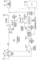
Fig. 2 means the key diagram of the schematic construction of the electric power supply cut-out circuit that the printer 10 of the first embodiment possesses.As shown in the figure, electric power supply cut-out circuit comprises batch (-type) switch (tact switch) 12, smmothing capacitor 13, resistor 13R, switching circuit 14, switch controlling signal generative circuit 15 and potential difference testing circuit 16.Switch controlling signal generative circuit 15 comprises latch cicuit 15a.Latch cicuit 15a is grounded.
Batch (-type) switch 12 comprises input terminal 12a, lead-out terminal 12b and operating portion 12c.Batch (-type) switch 12 is to switch the mains switch of connection status for the handover operation by become the posture of the 12c of handover operation section between the prime of on-state and second that connection status becomes off-state in the connection status of input terminal 12a and lead-out terminal 12b (below, also referred to as connection status).Only otherwise carry out handover operation, batch (-type) switch 12 will keep posture and the connection status of operating portion 12c.Input terminal 12a is connected with AC adapter 20.
Switch controlling signal generative circuit 15 is based on latching commencing signal VLT and latching ring off signal VRST from 16 inputs of potential difference testing circuit from 18 inputs of CPU17 or error detect circuit, generate switch controlling signal VSC, and this switch controlling signal VSC is exported to switching circuit 14.In the present embodiment, thereby, in during latching in latch cicuit 15a to latch cicuit 15a input and latch commencing signal VLT that commencing signal VLT is latched, switch controlling signal generative circuit 15 generates and should cut off the switch controlling signal VSC that direct current power is provided to internal circuit.Input while latching ring off signal VRST, latch cicuit 15a removes and latchs.Then, latch in latch cicuit 15a that commencing signal VLT is not latched during in, switch controlling signal generative circuit 15 does not generate and should cut off the switch controlling signal VSC that direct current power is provided to internal circuit.In addition, latch cicuit 15a utilizes the voltage Vin2 of the rear class of the batch (-type) switch 12 of inputting from AC adapter 20 via resistor 13R to be moved.
Potential difference testing circuit 16 detects the input terminal 12a of batch (-type) switch 12 and the potential difference Δ V (Vin1-Vin2) between lead-out terminal 12b, and the potential difference between two terminals be more than setting (for example, more than 1 (V)) situation under, will latch ring off signal VRST and export to switch controlling signal generative circuit 15.That is, potential difference testing circuit 16 becomes off-state at batch (-type) switch 12, and the input terminal 12a of batch (-type) switch 12 and the potential difference Δ V between lead-out terminal 12b become in the above situation of setting, output latch ring off signal VRST.
When pattern shifts as the power cut pattern from the electric power supply model, CPU17 will latch commencing signal VLT and export to potential difference testing circuit 16.In the situation that the pattern of printer 10 is the electric power supply model, error detect circuit 18 detects the mistake of the regulation in printer 10 inside, and when detecting this mistake, to switch controlling signal generative circuit 15 output latch commencing signal VLT.The mistake detected as error detect circuit 18, for example, can enumerate overvoltage mistake, low-voltage mistake, short circuit mistake etc.CPU17 and error detect circuit 18 are equivalent to the control part in " summary of the invention ".
A3. electric power is supplied with the action of cutting off circuit:
Fig. 3 means that the electric power in the printer 10 of the first embodiment supplies with the sequential chart of the action of cutting off circuit.
The moment t0 that is off-state at batch (-type) switch 12, if the posture of the operating portion 12c of batch (-type) switch 12 switches to prime and batch (-type) switch 12 becomes on-state from second, voltage Vin2 rises, and the pattern of printer 10 becomes the electric power supply model.
Afterwards, CPU17 is with reference to timer, if from personal computer PC, do not drop into presswork and directly pass through the stipulated time, at moment t1, for the pattern by printer 10 shifts as power cut pattern, output latch commencing signal VLT from the electric power supply model.If latch cicuit 15a latchs commencing signal VLT to this and latched (latch mode: latch effectively), switch controlling signal generative circuit 15 should cut off to switching circuit 14 outputs the switch controlling signal VSC that direct current power is provided to internal circuit.If this switch controlling signal VSC is input to switching circuit 14, switching circuit 14 becomes open mode.Become open mode at switching circuit 14, cut off after internal circuit provides direct current power, batch (-type) switch 12 is switched to off-state, until again switch to on-state, the pattern of printer 10 is still the power cut pattern.
For the pattern that makes printer 10 is the electric power supply model from the power cut pattern recovery, if at moment t3, the posture of the operating portion 12c of batch (-type) switch 12 is switched to second and batch (-type) switch 12 becomes off-state from prime, the residual charge due to smmothing capacitor 13 is discharged via resistor 13R and latch cicuit 15a etc., so the voltage (voltage Vin2) between two terminals of smmothing capacitor 13 can reduce.Therefore, can produce potential difference between the input terminal 12a of batch (-type) switch 12 and lead-out terminal 12b.Input terminal 12a and the potential difference between lead-out terminal 12b that potential difference testing circuit 16 detects batch (-type) switch 12 become the above situation of setting, thereby will latch ring off signal VRST, output to switch controlling signal generative circuit 15.If this latchs ring off signal VRST and is input to latch cicuit 15a and removes and latch (latch mode: invalid), switch controlling signal generative circuit 15 stop output should cutting off the switch controlling signal VSC that direct current power is provided to internal circuit.If should cut off to internal circuit, provide the input of the switch controlling signal VSC of direct current power to stop, switching circuit 14 becomes closure state.
And if, at moment t4, the posture of the operating portion 12c of batch (-type) switch 12 switches to prime and batch (-type) switch 12 becomes on-state from second, the pattern of printer 10 returns to the electric power supply model.In addition, in the present embodiment, above-mentioned moment t3 to time interval of t4 constantly be for example about 0.5 second, as the switching time of the operating portion 12c in batch (-type) switch 12 be the shorter time.Therefore, at moment t3, in during t4 constantly, the residual charge of smmothing capacitor 13 is discharged via resistor 13R and latch cicuit 15a etc., but at moment t4, and voltage Vin2 can not reduce to such an extent that be less than the operation voltage of latch cicuit 15a.
In addition, as previously described above, in the situation that the pattern of printer 10 is the electric power supply model, error detect circuit 18 detects the mistake of the regulation in printer 10 inside, and when detecting this mistake, to switch controlling signal generative circuit 15 output latch commencing signal VLT.Although omitted diagram, now, electric power supply with to cut off circuit carry out with in moment t1 identical action during from CPU17 output latch commencing signal VLT, the pattern of printer 10 switches to the power cut pattern from the electric power supply model.
A4. effect:
Here, for the printer 10 that means the first embodiment cuts off because comprising that the electric power with said structure is supplied with the effect that circuit produces, illustrate that the electric power in the printer in the past that has electric power supply model and power cut pattern as pattern is supplied with the cut-out circuit.
Fig. 4 means the key diagram of the schematic construction of the electric power supply cut-out circuit that printer in the past possesses.From Fig. 4 and Fig. 2 relatively, this electric power is supplied with electric power that the printer 10 that cuts off circuit and the first embodiment possesses and is supplied with the difference of cut-out circuit and be: comprise the discharge circuit with discharge resistance R and switching circuit SW; Do not possess potential difference testing circuit 16; Do not possess error detect circuit 18.In addition, discharge circuit is the circuit of the residual charge electric discharge for move to make smmothing capacitor 13 when on-state switches to off-state at batch (-type) switch 12.
Fig. 5 means the sequential chart that the action of circuit is cut off in the electric power supply in printer in the past.Action from moment t0 to moment t3 supplies with the electric power the printer 10 of the first embodiment the action identical (with reference to Fig. 3) of cutting off circuit.
Electric power in printer is in the past supplied with and is cut off in circuit, if at moment t3, batch (-type) switch 12 becomes off-state, and discharge circuit is moved, and the residual charge of smmothing capacitor 13 is discharged.Afterwards, if at moment t5, the voltage (voltage Vin2) between two terminals of smmothing capacitor 13 reduces to such an extent that be less than the operation voltage of latch cicuit 15Ra, and latching of latch cicuit 15Ra is disengaged (latch mode: invalid).Latch releasing by this, switching circuit 14 becomes closure state.Then, at moment t6, when batch (-type) switch 12 switches to on-state again, to internal circuit, provide direct current power.
; electric power in printer is in the past supplied with and is cut off in circuit; until the voltage between two terminals of smmothing capacitor 13 is less than the operation voltage of latch cicuit 15Ra, latch cicuit 15Ra can not be disengaged and latch, and switching circuit 14 is still in open mode.Therefore, even must be less than the moment t4 before the operation voltage of latch cicuit 15Ra at the lower voltage between two terminals of smmothing capacitor 13, batch (-type) switch 12 is switched to on-state, and switching circuit 14, still in open mode, can not provide direct current power to internal circuit.
In order to eliminate such unfavorable condition, think and use the as far as possible little and resistor that permissible loss is large as far as possible of resistance value to be used as the discharge resistance R that discharge circuit possesses, can shorten latching the releasing time of latch cicuit 15Ra.But, because the resistor general appearance size with such characteristic is larger, so can cause printer to maximize as discharge resistance R such resistor.Therefore, there is the resistor of above-mentioned characteristic and be not suitable for carrying in printer.
With respect to this, in the printer 10 of the first embodiment, because electric power supply cut-out circuit possesses potential difference testing circuit 16, so can be according to the releasing of latching that ring off signal VRST carries out latch cicuit 15a of latching from 16 outputs of potential difference testing circuit.Therefore, in the printer 10 of the first embodiment, need to not be used as discharge resistance R in order to shorten the resistance value that resistance value is little and permissible loss is large that latchs the releasing time and will illustrate before.That is,, by the printer 10 of the first embodiment, can take into account the miniaturization of printer 10 and latch the shortening of releasing time.
In addition, in the printer 10 of the first embodiment, when error detect circuit 18 detects regulation wrong, can output latch commencing signal VLT cut off to internal circuit direct current power is provided, so, in the situation that fault has occurred in internal circuit, can prevent the expansion of this fault.
In addition, in the printer 10 of the first embodiment, can consider smmothing capacitor 13 residual charge when electric discharge power consumption and set electric power discharge time and supply with the resistance value of cutting off the resistor 13R in circuit.Therefore, the operating current of latch cicuit 15a while by suitable setting pattern, being the power cut pattern, flow through the electric current of resistor 13R, thereby produce time till the above potential difference of afore mentioned rules value (detect potential difference till time) in the time of can suitably being set in batch (-type) switch 12 and switching to off-state between the input terminal 12a of batch (-type) switch 12 and lead-out terminal 12b.
B. the second embodiment:
The printer 10 of the printer of the second embodiment and the first embodiment similarly, has electric power supply model and power cut pattern as pattern.Wherein, the electric power of the printer of the second embodiment is supplied with the printer 10 that the structure of cutting off circuit is different from the first embodiment.Below, illustrate that the electric power in the printer of the second embodiment is supplied with structure and the action of cutting off circuit.
B1. electric power is supplied with the structure of cutting off circuit:
Fig. 6 means the key diagram of the schematic construction of the electric power supply cut-out circuit that the printer of the second embodiment possesses.From Fig. 6 and Fig. 2 relatively, in the printer of the second embodiment, electric power is supplied with and is cut off circuit and replace the switch controlling signal generative circuit 15 in the first embodiment and possess switch controlling signal generative circuit 15A.And switch controlling signal generative circuit 15A, except latch cicuit 15a, also possesses to latch and removes inhibit circuit 15b.In addition, CPU17 the pattern of printer 10 be the electric power supply model during, remove inhibit circuit 15b output latch releasing inhibit signal VPR to latching, when pattern is transferred to the power cut pattern from the electric power supply model, stop latching the output (with reference to Fig. 7) of removing inhibit signal VPR.Latch remove inhibit circuit 15b input and latch remove inhibit signal VPR during, that forbids to latch cicuit 15a output from the potential difference testing circuit 16 outputs latchs ring off signal VRST.In addition, except above-mentioned structure, other are identical with the first embodiment.
B2. electric power is supplied with the action of cutting off circuit:
Fig. 7 means that the electric power in the printer of the second embodiment supplies with the sequential chart of the action of cutting off circuit.It is roughly the same that electric power in the second embodiment is supplied with the action and the first embodiment that cut off circuit.Wherein, electric power is in a second embodiment supplied with and is cut off in circuit, remove inhibit circuit 15b owing to possessing to latch, thus pattern be the electric power supply model during, can be to latch cicuit 15a input from the potential difference testing circuit 16 outputs latch ring off signal VRST.
In the situation that pattern is the electric power supply model, even batch (-type) switch 12 is on-state sometimes, also can produce the input terminal 12a of batch (-type) switch 12 and the potential difference between lead-out terminal 12b.For example, because the sulfuration of the contact component in batch (-type) switch 12 or the deterioration of adhering to the contact of siloxanes etc. cause that contact resistance increases, thereby as in Fig. 7 with single-point line encirclement, cause more than its potential difference becomes setting.And, even under these circumstances, potential difference testing circuit 16 also with batch (-type) switch 12 situation that is off-state similarly, output latch ring off signal VRST (with reference to Fig. 7 latch ring off signal VRST).Therefore, as the switch controlling signal generative circuit 15 in the first embodiment, in the situation that do not possess to latch, remove inhibit circuit 15b, may cause the unfavorable condition that latchs ring off signal VRST of not expecting to switch controlling signal generative circuit 15A input.With respect to this, in the printer of the second embodiment, supply with by electric power the switch controlling signal generative circuit 15A cut off in circuit and possess to latch and remove inhibit circuit 15b, what can prevent that input from not expecting latchs the such unfavorable condition of ring off signal.
Printer by the second embodiment described above, with the printer 10 of the first embodiment, similarly do not use discharge resistance R yet, but can be according to the releasing of latching that ring off signal VRST carries out latch cicuit 15a of latching from potential difference testing circuit 16 output, so can take into account the miniaturization of printer and latch the shortening of releasing time.
C. the 3rd embodiment:
The printer of the printer of the 3rd embodiment and the second embodiment similarly has electric power supply model and power cut pattern as pattern.Wherein, the electric power of the printer of the 3rd embodiment is supplied with the printer that the structure of cutting off circuit is different from the second embodiment.Below, illustrate that the electric power in the printer of the 3rd embodiment is supplied with structure and the action of cutting off circuit.
C1. electric power is supplied with the structure of cutting off circuit:
Fig. 8 means the key diagram of the schematic construction of the electric power supply cut-out circuit that the printer of the 3rd embodiment possesses.From Fig. 8 and Fig. 6 relatively, in the printer of the 3rd embodiment, electric power is supplied with and is cut off circuit and replace the switch controlling signal generative circuit 15A in the second embodiment and possess switch controlling signal generative circuit 15B.And switch controlling signal generative circuit 15B, except latch cicuit 15a removes inhibit circuit 15b with latching, also has OR circuit 15c.And, to OR circuit 15c input from latch cicuit 15a the status signal VST of the latch mode of the expression latch cicuit 15a of output and passed through to latch remove inhibit circuit 15b latch ring off signal VRST.In addition, status signal VST is the signal identical with switch controlling signal VSC in the second embodiment.Switch controlling signal generative circuit 15B will export to switching circuit 14 as switch controlling signal VSC from the signal of OR circuit 15c output.
; from latch cicuit 15a to OR circuit 15c input mean to latch status signal VST that commencing signal VLT latched during; perhaps from latch remove inhibit circuit 15b input and latch ring off signal VRST during, switch controlling signal generative circuit 15B generates should cut off the switch controlling signal VSC that direct current power is provided to internal circuit.In addition, not to OR circuit 15c input mean to latch the status signal VST that commencing signal VLT latched and latch these two signals of ring off signal VRST during, switch controlling signal generative circuit 15B can not generate and should cut off the switch controlling signal VSC that direct current power is provided to internal circuit.
C2. electric power is supplied with the action of cutting off circuit:
Fig. 9 means that the electric power in the printer of the 3rd embodiment supplies with the sequential chart of the action of cutting off circuit.Constantly t0 supplies with the action identical (with reference to Fig. 7) of cut-out circuit to the electric power in the printer of the action of t3 constantly and the second embodiment.
Electric power in the printer of the second embodiment illustrated is before supplied with and is cut off in circuit, if the moment t3 that is the power cut pattern in pattern, batch (-type) switch 12 becomes off-state, latch cicuit 15a is disengaged and latchs by latching ring off signal VRST, so switching circuit 14 becomes closure state.Therefore, even batch (-type) switch 12 is off-state, also exist electric current to flow to from smmothing capacitor 13 internal circuit that comprises CPU17, thereby internal circuit carry out the hidden danger of malfunction.
With respect to this, electric power in the printer of the 3rd embodiment is supplied with and is cut off in circuit, due to OR circuit 15c input and latch ring off signal VRST, so can not produce such malfunction.; if at moment t3; batch (-type) switch 12 becomes off-state; potential difference testing circuit 16 detects input terminal 12a and the potential difference between lead-out terminal 12b the output latch ring off signal VRST of batch (-type) switch 12, and this latchs ring off signal VRST and be input to OR circuit 15c after latching releasing inhibit circuit 15b.And, as switching circuit 14 being made as to the switch controlling signal VSC of open mode, from switch controlling signal generative circuit 15B to switching circuit 14 this latch ring off signal VRST, so switching circuit 14 can be remained to open mode.Therefore, can prevent the malfunction of above-mentioned internal circuit.
In addition, electric power in the printer of the 3rd embodiment is supplied with and is cut off in circuit, omitted and latched in the situation of removing inhibit circuit 15b, as meaned with the single-point line in Fig. 9, in the situation that more than the potential difference produced between the input terminal 12a of batch (-type) switch 12 and lead-out terminal 12b becomes setting, from potential difference testing circuit 16 output latch ring off signal VRST.And, as switch controlling signal VSC, export this from switch controlling signal generative circuit 15B (OR circuit 15c) and latch ring off signal VRST.Therefore, pattern be the electric power supply model during, exist switching circuit 14 to become the situation of open mode.But, in the present embodiment, remove inhibit circuit 15b owing to possessing to latch, so can not produce above-mentioned unfavorable condition.
Printer by the 3rd embodiment described above, also with the printer of the printer 10 of the first embodiment and the second embodiment similarly, do not use discharge resistance R, but can be according to the releasing of latching that ring off signal VRST carries out latch cicuit 15a of latching from potential difference testing circuit 16 output, so can take into account the miniaturization of printer and latch the shortening of releasing time.
D. variation:
Above, several execution mode of the present invention has been described, but the present invention is not limited to such execution mode, in the scope that does not break away from its purport, can implement by variety of way.For example, can carry out following distortion.
D1. variation 1:
In the printer 10 of above-mentioned the first embodiment, electric power is supplied with the cut-out circuit and is possessed potential difference testing circuit 16, and this potential difference testing circuit 16 will latch ring off signal VRST and export to switch controlling signal generative circuit 15, but the present invention is not limited to this.Electric power is supplied with the cut-out circuit also can possess the ring off signal of latching generating unit, this latchs the ring off signal generating unit and detects the input terminal 12a of batch (-type) switch 12 and the connection status of lead-out terminal 12b, in the situation that this connection status is off-state, will latchs ring off signal VRST and export to switch controlling signal generative circuit 15.
Figure 10 means that the electric power in the printer of variation supplies with the key diagram of the schematic construction of cutting off circuit.From Figure 10 and Fig. 2 relatively, the electric power in the printer of variation is supplied with and is cut off circuit and replace the potential difference testing circuit 16 in the first embodiment and comprise transducer 16s.This transducer 16s detects batch (-type) switch 12 and is set to off-state, still is set to on-state.And, when batch (-type) switch 12 is set to off-state, transducer 16s will latch ring off signal VRST and export to switch controlling signal generative circuit 15.In addition, when batch (-type) switch 12 is set to on-state, transducer 16s can not export to switch controlling signal generative circuit 15 by latching ring off signal VRST.In addition, transducer 16s be so long as can detect batch (-type) switch 12 and be set to the transducer that off-state still is set to on-state and get final product, for example, and can the Application Optics transducer, the various transducers such as ultrasonic sensor.Be made as above-mentioned structure by electric power being supplied with to the cut-out circuit, also can play the effect identical with the printer 10 of the first embodiment.
D2. variation 2:
In the above-described embodiments, at electric power, supply with to cut off in the latch cicuit 15a that circuit possesses, inputted from error detect circuit 18 outputs latch commencing signal VLT, but also can omit this situation.
D3. variation 3:
In the above-described embodiments, as electric power, supply with and cut off the mains switch that circuit possesses, used batch (-type) switch 12, but the present invention is not limited to this.In the present invention, generally, mains switch is so long as get final product as the switch of Types Below: the mains switch with input terminal, lead-out terminal and operating portion, become the handover operation of the posture of handover operation section between the prime of on-state and second that connection status becomes off-state by the connection status at input terminal and lead-out terminal, the switching connection status, and only otherwise carry out handover operation, the posture of operating portion and connection status will be held.As such switch, such as enumerating toggle switch (toggle-switch), slide switch (slide switch), rocker switch (rocker switch) etc.
D4. variation 4:
In the above-described embodiments, the situation that applies the present invention to printer has been described, but also can be applied in other information equipments beyond printer.
Claims (6)
1. an information equipment, the control part that utilizes the direct current power from being connected to outside supply unit and providing to be moved is provided, and have as pattern: the first pattern of described direct current power is provided and cuts off the second pattern that described direct current power is provided to described control part to described control part, this information equipment comprises:
Mains switch, it has input terminal, lead-out terminal and operating portion, in described mains switch, described input terminal is connected with described supply unit, become the handover operation of the posture of the described operating portion of switching between the prime of on-state and second that described connection status becomes off state by the connection status at described input terminal and described lead-out terminal, switch described connection status, and only otherwise carry out described handover operation, keep posture and the described connection status of described operating portion;
Smmothing capacitor, it has the first terminal and the second terminal, and described the first terminal is connected with the described lead-out terminal of described mains switch, and described the second terminal is grounded;
Switching circuit, it is connected with the described lead-out terminal of described mains switch, and the providing and cutting off to the described direct current power of described control part for switching;
The switch controlling signal generative circuit, it has the latch cicuit that commencing signal is latched that latchs from described control part input, and the described latch mode that latchs commencing signal based in described latch cicuit at least, generation should be cut off the switch controlling signal that described direct current power is provided to described control part, and outputs to described switching circuit; And
Latch the ring off signal generating unit, it detects the described connection status in described mains switch, and in the situation that described connection status is off state, the described ring off signal of latching of latching of latching commencing signal that should remove in described latch cicuit outputs to described switch controlling signal generative circuit
Described latch cicuit and the described ring off signal generating unit that latchs are configured to and can utilize from the described lead-out terminal of described mains switch or the described direct current power that provides from described smmothing capacitor and be moved,
When described pattern is transferred to described the second pattern from described the first pattern, described control part outputs to described switch controlling signal generative circuit by the described commencing signal that latchs,
To described latch cicuit, input describedly while latching ring off signal, described latch cicuit is removed described the latching of commencing signal of latching,
When having inputted described switch controlling signal, described switching circuit becomes open mode,
When not inputting described switch controlling signal, described switching circuit becomes closure state,
The described ring off signal generating unit that latchs comprises: the potential difference testing circuit, this potential difference testing circuit detects the described input terminal of described mains switch and the potential difference between described lead-out terminal, and in the situation that described potential difference is more than setting, the situation that is off state as described connection status, latch ring off signal and output to described switch controlling signal generative circuit described.
2. information equipment according to claim 1, wherein,
Between the described the first terminal of described smmothing capacitor and the power supply terminal of described latch cicuit, via resistor, connect,
When the connection status of the input terminal of described mains switch and lead-out terminal becomes off state, the resistance value of described resistor is set as to the value that the residual charge of smmothing capacitor discharges in official hour.
3. information equipment according to claim 2, wherein,
Described control part, further described pattern be described the first pattern during, remove inhibit signal to described switch controlling signal generative circuit output latch, and when described pattern is transferred to described the second pattern from described the first pattern, stop the described output that removing inhibit signal of latching
Described switch controlling signal generative circuit also comprises:
Latch the releasing inhibit circuit, its inputted described latch remove inhibit signal during, forbid latching ring off signal to described latch cicuit input is described.
4. information equipment according to claim 3, wherein,
Described switch controlling signal generative circuit consists of the OR circuit,
At least input and mean that described latch cicuit latchs status signal that commencing signal latched and latchs remove inhibit circuit output described and latch ring off signal from described described to described OR circuit,
To as described switch controlling signal, export from the signal of described OR circuit output.
5. according to the described information equipment of any one of claim 1 to 4, wherein,
Described control part also comprises: wrong detection unit, and this wrong detection unit detects the mistake of the regulation in described information equipment,
When detecting described mistake, described wrong detection unit outputs to described switch controlling signal generative circuit by the described commencing signal that latchs.
6. according to the described information equipment of any one of claim 1 to 4, wherein,
Described information equipment is printer.
Priority Applications (1)
| Application Number | Priority Date | Filing Date | Title |
|---|---|---|---|
| CN201310722224.9A CN103701317B (en) | 2009-11-13 | 2010-11-12 | Information device |
Applications Claiming Priority (2)
| Application Number | Priority Date | Filing Date | Title |
|---|---|---|---|
| JP2009259647A JP5633139B2 (en) | 2009-11-13 | 2009-11-13 | Information equipment |
| JP2009-259647 | 2009-11-13 |
Related Child Applications (1)
| Application Number | Title | Priority Date | Filing Date |
|---|---|---|---|
| CN201310722224.9A Division CN103701317B (en) | 2009-11-13 | 2010-11-12 | Information device |
Publications (2)
| Publication Number | Publication Date |
|---|---|
| CN102064698A CN102064698A (en) | 2011-05-18 |
| CN102064698B true CN102064698B (en) | 2013-12-11 |
Family
ID=43608688
Family Applications (2)
| Application Number | Title | Priority Date | Filing Date |
|---|---|---|---|
| CN2010105487858A Active CN102064698B (en) | 2009-11-13 | 2010-11-12 | Information device |
| CN201310722224.9A Active CN103701317B (en) | 2009-11-13 | 2010-11-12 | Information device |
Family Applications After (1)
| Application Number | Title | Priority Date | Filing Date |
|---|---|---|---|
| CN201310722224.9A Active CN103701317B (en) | 2009-11-13 | 2010-11-12 | Information device |
Country Status (5)
| Country | Link |
|---|---|
| US (2) | US8736116B2 (en) |
| EP (1) | EP2336843B1 (en) |
| JP (1) | JP5633139B2 (en) |
| KR (1) | KR101755678B1 (en) |
| CN (2) | CN102064698B (en) |
Families Citing this family (16)
| Publication number | Priority date | Publication date | Assignee | Title |
|---|---|---|---|---|
| JP5421209B2 (en) * | 2010-08-27 | 2014-02-19 | 株式会社沖データ | Power supply control circuit and image forming apparatus having power supply control circuit |
| TWI590038B (en) * | 2011-04-25 | 2017-07-01 | 緯創資通股份有限公司 | Power control device and electronic device using the same |
| JP6041522B2 (en) * | 2012-04-18 | 2016-12-07 | キヤノン株式会社 | Information processing apparatus, information processing apparatus control method, program, and storage medium |
| CN104902533B (en) | 2015-04-30 | 2016-12-28 | 广东欧珀移动通信有限公司 | A kind of method for network access and mobile communication terminal |
| JP6634904B2 (en) * | 2016-03-16 | 2020-01-22 | セイコーエプソン株式会社 | Electronic device and electronic device control method |
| US9984011B2 (en) | 2016-06-06 | 2018-05-29 | Qualcomm Incorporated | Termination schemes for multi-rank memory bus architectures |
| KR102577409B1 (en) * | 2016-08-22 | 2023-09-14 | 엘지디스플레이 주식회사 | Controller, display device, and the method for driving the display device |
| US9767889B1 (en) * | 2017-02-15 | 2017-09-19 | Qualcomm Incorporated | Programmable pad capacitance for supporting bidirectional signaling from unterminated endpoints |
| EP3572889B1 (en) * | 2017-02-17 | 2021-07-07 | Huawei Technologies Co., Ltd. | Control circuit and circuit control method |
| KR102298069B1 (en) | 2017-03-10 | 2021-09-03 | 삼성전자주식회사 | Method and Apparatus for Managing Battery |
| JP6473980B2 (en) * | 2017-06-13 | 2019-02-27 | ファナック株式会社 | unit |
| JP2019034430A (en) * | 2017-08-10 | 2019-03-07 | 東芝テック株式会社 | Printer and program |
| GB2584650A (en) * | 2019-06-06 | 2020-12-16 | Things On Edge Ltd | Electronic devices |
| CN110544934A (en) * | 2019-09-05 | 2019-12-06 | 珠海格力电器股份有限公司 | converter control method and device for improving response speed and converter equipment |
| US11597486B1 (en) * | 2019-12-18 | 2023-03-07 | Brunswick Corporation | Tiller for outboard motor |
| CN111580428B (en) * | 2020-04-29 | 2022-07-29 | 上海空间电源研究所 | Instruction sending circuit |
Citations (3)
| Publication number | Priority date | Publication date | Assignee | Title |
|---|---|---|---|---|
| CN1327289A (en) * | 2000-06-01 | 2001-12-19 | 索尼公司 | Power supply equipment and method |
| CN1691452A (en) * | 2004-04-20 | 2005-11-02 | 富士通株式会社 | Power saving control method and device in electronic device, and power saving electronic device |
| CN101398674A (en) * | 2007-09-28 | 2009-04-01 | 群康科技(深圳)有限公司 | Electric power circuit and control method thereof |
Family Cites Families (18)
| Publication number | Priority date | Publication date | Assignee | Title |
|---|---|---|---|---|
| US5182546A (en) * | 1988-02-12 | 1993-01-26 | Canon Kabushiki Kaisha | Electronic apparatus which can discriminate between different power sources which it uses |
| WO1996036099A2 (en) * | 1995-05-11 | 1996-11-14 | Ericsson Inc. | Power control circuit for a battery operated device |
| US5936317A (en) * | 1996-04-09 | 1999-08-10 | Harness System Technologies Research, Ltd. | Power supply device for vehicle |
| US5854551A (en) * | 1997-02-26 | 1998-12-29 | Ericsson Inc. | Battery charger with low standby current |
| JP3901782B2 (en) * | 1997-02-26 | 2007-04-04 | インターナショナル・ビジネス・マシーンズ・コーポレーション | Power supply device and electronic device for preventing leakage current |
| JP3233075B2 (en) * | 1997-08-06 | 2001-11-26 | 株式会社豊田自動織機 | Switching power supply |
| JP2001016863A (en) * | 1999-06-25 | 2001-01-19 | Matsushita Electric Works Ltd | Electric power unit |
| JP2001037078A (en) * | 1999-07-16 | 2001-02-09 | Alps Electric Co Ltd | Low power consumption on-vehicle control equipment |
| DE10001394A1 (en) * | 2000-01-14 | 2001-07-26 | Infineon Technologies Ag | Circuit for applying clocked supply voltage to load requires no auxiliary winding, discrete components; very small power losses arise in applying supply voltage - has switch connected between load and control circuit's first voltage supply connection with control connection to which drive signal is applied |
| JP2001309655A (en) | 2000-04-19 | 2001-11-02 | Sanken Electric Co Ltd | Switching power supply device having protection function for overloading |
| US6754092B2 (en) * | 2002-06-27 | 2004-06-22 | International Business Machines Corporation | Method and apparatus for reducing power consumption for power supplied by a voltage adapter |
| JP4096297B2 (en) * | 2002-06-28 | 2008-06-04 | 株式会社リコー | Protection circuit, DC / DC converter and timer latch circuit |
| JP4108457B2 (en) | 2002-11-27 | 2008-06-25 | シャープ株式会社 | Switching power supply |
| JP2006166561A (en) | 2004-12-06 | 2006-06-22 | Canon Inc | Power supply device |
| JP2006166580A (en) * | 2004-12-07 | 2006-06-22 | Canon Inc | Switching power supply unit |
| JP2006073023A (en) * | 2005-09-15 | 2006-03-16 | Konica Minolta Holdings Inc | Power saving control device |
| US7852645B2 (en) * | 2007-12-12 | 2010-12-14 | Avago Technologies Ecbu Ip (Singapore) Pte. Ltd. | Circuit and associated method for reducing power consumption in a power transformer |
| JP2009165288A (en) * | 2008-01-08 | 2009-07-23 | Sanken Electric Co Ltd | Switching power supply device |
-
2009
- 2009-11-13 JP JP2009259647A patent/JP5633139B2/en active Active
-
2010
- 2010-10-29 US US12/915,498 patent/US8736116B2/en active Active
- 2010-11-11 KR KR1020100112098A patent/KR101755678B1/en active IP Right Grant
- 2010-11-12 EP EP10191095.8A patent/EP2336843B1/en active Active
- 2010-11-12 CN CN2010105487858A patent/CN102064698B/en active Active
- 2010-11-12 CN CN201310722224.9A patent/CN103701317B/en active Active
-
2014
- 2014-04-07 US US14/246,993 patent/US9208981B2/en active Active
Patent Citations (3)
| Publication number | Priority date | Publication date | Assignee | Title |
|---|---|---|---|---|
| CN1327289A (en) * | 2000-06-01 | 2001-12-19 | 索尼公司 | Power supply equipment and method |
| CN1691452A (en) * | 2004-04-20 | 2005-11-02 | 富士通株式会社 | Power saving control method and device in electronic device, and power saving electronic device |
| CN101398674A (en) * | 2007-09-28 | 2009-04-01 | 群康科技(深圳)有限公司 | Electric power circuit and control method thereof |
Non-Patent Citations (1)
| Title |
|---|
| JP特开2006-166561A 2006.06.22 |
Also Published As
| Publication number | Publication date |
|---|---|
| KR101755678B1 (en) | 2017-07-07 |
| EP2336843B1 (en) | 2018-10-31 |
| JP2011109746A (en) | 2011-06-02 |
| US9208981B2 (en) | 2015-12-08 |
| US20140217834A1 (en) | 2014-08-07 |
| US20110115307A1 (en) | 2011-05-19 |
| JP5633139B2 (en) | 2014-12-03 |
| CN102064698A (en) | 2011-05-18 |
| US8736116B2 (en) | 2014-05-27 |
| CN103701317B (en) | 2017-05-24 |
| EP2336843A3 (en) | 2017-08-02 |
| CN103701317A (en) | 2014-04-02 |
| EP2336843A2 (en) | 2011-06-22 |
| KR20110053194A (en) | 2011-05-19 |
Similar Documents
| Publication | Publication Date | Title |
|---|---|---|
| CN102064698B (en) | Information device | |
| CN106292341B (en) | A kind of power on/off system and method | |
| CN104769841B (en) | For reducing the clock gating circuit of dynamic power | |
| CN102545574B (en) | Low-power consumption power network designing method for system on chip (SOC) chip | |
| US8032259B2 (en) | Bi-directional power control | |
| CN103545912A (en) | Power supply switching circuit, real time clock device, electronic apparatus, mobile unit, and method of controlling power supply switching circuit | |
| WO2009099499A3 (en) | State retaining power gated latch and method therefor | |
| CN102377416A (en) | Power supply resetting circuit | |
| CN108028643A (en) | Utilize the power sharing of trigger | |
| EP2100206B1 (en) | Systems, circuits, chips and methods with protection at power island boundaries | |
| JP2013196693A (en) | Electronic equipment provided with standby mode | |
| US7847441B2 (en) | Semiconductor integrated circuit | |
| CN102346529B (en) | Power supply control circuit | |
| JP6783758B2 (en) | Output discharge technique for load switches | |
| CN100487996C (en) | User operating blocking-up device | |
| CN202025278U (en) | CMOS (complementary metal oxide semiconductor) clear circuit of mainboard | |
| CN115425716A (en) | Electronic device | |
| TWI410787B (en) | Power control unit | |
| CN102096454A (en) | Startup/shutdown circuit | |
| JP2005289204A (en) | Power supply control device | |
| CN100517277C (en) | Flash memory protection module and closing method thereof | |
| CN216979719U (en) | USB power supply switching circuit and USB power supply device | |
| CN110727303B (en) | Power supply apparatus having electronic circuit breaker and control method thereof | |
| CN100444490C (en) | Operation blocker and blocking method for user | |
| US20190229731A1 (en) | Power gating circuit for holding data in logic block |
Legal Events
| Date | Code | Title | Description |
|---|---|---|---|
| C06 | Publication | ||
| PB01 | Publication | ||
| C10 | Entry into substantive examination | ||
| SE01 | Entry into force of request for substantive examination | ||
| C14 | Grant of patent or utility model | ||
| GR01 | Patent grant |