CN101476710B - Illuminating device and its manufacture method - Google Patents
Illuminating device and its manufacture method Download PDFInfo
- Publication number
- CN101476710B CN101476710B CN2009100096747A CN200910009674A CN101476710B CN 101476710 B CN101476710 B CN 101476710B CN 2009100096747 A CN2009100096747 A CN 2009100096747A CN 200910009674 A CN200910009674 A CN 200910009674A CN 101476710 B CN101476710 B CN 101476710B
- Authority
- CN
- China
- Prior art keywords
- led element
- light
- submounts
- luminescent device
- glass
- Prior art date
- Legal status (The legal status is an assumption and is not a legal conclusion. Google has not performed a legal analysis and makes no representation as to the accuracy of the status listed.)
- Expired - Fee Related
Links
Images


Classifications
-
- H—ELECTRICITY
- H01—ELECTRIC ELEMENTS
- H01L—SEMICONDUCTOR DEVICES NOT COVERED BY CLASS H10
- H01L2224/00—Indexing scheme for arrangements for connecting or disconnecting semiconductor or solid-state bodies and methods related thereto as covered by H01L24/00
- H01L2224/01—Means for bonding being attached to, or being formed on, the surface to be connected, e.g. chip-to-package, die-attach, "first-level" interconnects; Manufacturing methods related thereto
- H01L2224/10—Bump connectors; Manufacturing methods related thereto
- H01L2224/15—Structure, shape, material or disposition of the bump connectors after the connecting process
- H01L2224/16—Structure, shape, material or disposition of the bump connectors after the connecting process of an individual bump connector
- H01L2224/161—Disposition
- H01L2224/16151—Disposition the bump connector connecting between a semiconductor or solid-state body and an item not being a semiconductor or solid-state body, e.g. chip-to-substrate, chip-to-passive
- H01L2224/16221—Disposition the bump connector connecting between a semiconductor or solid-state body and an item not being a semiconductor or solid-state body, e.g. chip-to-substrate, chip-to-passive the body and the item being stacked
- H01L2224/16225—Disposition the bump connector connecting between a semiconductor or solid-state body and an item not being a semiconductor or solid-state body, e.g. chip-to-substrate, chip-to-passive the body and the item being stacked the item being non-metallic, e.g. insulating substrate with or without metallisation
-
- H—ELECTRICITY
- H01—ELECTRIC ELEMENTS
- H01L—SEMICONDUCTOR DEVICES NOT COVERED BY CLASS H10
- H01L2224/00—Indexing scheme for arrangements for connecting or disconnecting semiconductor or solid-state bodies and methods related thereto as covered by H01L24/00
- H01L2224/01—Means for bonding being attached to, or being formed on, the surface to be connected, e.g. chip-to-package, die-attach, "first-level" interconnects; Manufacturing methods related thereto
- H01L2224/42—Wire connectors; Manufacturing methods related thereto
- H01L2224/47—Structure, shape, material or disposition of the wire connectors after the connecting process
- H01L2224/48—Structure, shape, material or disposition of the wire connectors after the connecting process of an individual wire connector
- H01L2224/4805—Shape
- H01L2224/4809—Loop shape
- H01L2224/48091—Arched
-
- H—ELECTRICITY
- H01—ELECTRIC ELEMENTS
- H01L—SEMICONDUCTOR DEVICES NOT COVERED BY CLASS H10
- H01L2224/00—Indexing scheme for arrangements for connecting or disconnecting semiconductor or solid-state bodies and methods related thereto as covered by H01L24/00
- H01L2224/01—Means for bonding being attached to, or being formed on, the surface to be connected, e.g. chip-to-package, die-attach, "first-level" interconnects; Manufacturing methods related thereto
- H01L2224/42—Wire connectors; Manufacturing methods related thereto
- H01L2224/47—Structure, shape, material or disposition of the wire connectors after the connecting process
- H01L2224/48—Structure, shape, material or disposition of the wire connectors after the connecting process of an individual wire connector
- H01L2224/481—Disposition
- H01L2224/48151—Connecting between a semiconductor or solid-state body and an item not being a semiconductor or solid-state body, e.g. chip-to-substrate, chip-to-passive
- H01L2224/48221—Connecting between a semiconductor or solid-state body and an item not being a semiconductor or solid-state body, e.g. chip-to-substrate, chip-to-passive the body and the item being stacked
- H01L2224/48245—Connecting between a semiconductor or solid-state body and an item not being a semiconductor or solid-state body, e.g. chip-to-substrate, chip-to-passive the body and the item being stacked the item being metallic
- H01L2224/48247—Connecting between a semiconductor or solid-state body and an item not being a semiconductor or solid-state body, e.g. chip-to-substrate, chip-to-passive the body and the item being stacked the item being metallic connecting the wire to a bond pad of the item
-
- H—ELECTRICITY
- H01—ELECTRIC ELEMENTS
- H01L—SEMICONDUCTOR DEVICES NOT COVERED BY CLASS H10
- H01L2224/00—Indexing scheme for arrangements for connecting or disconnecting semiconductor or solid-state bodies and methods related thereto as covered by H01L24/00
- H01L2224/01—Means for bonding being attached to, or being formed on, the surface to be connected, e.g. chip-to-package, die-attach, "first-level" interconnects; Manufacturing methods related thereto
- H01L2224/42—Wire connectors; Manufacturing methods related thereto
- H01L2224/47—Structure, shape, material or disposition of the wire connectors after the connecting process
- H01L2224/48—Structure, shape, material or disposition of the wire connectors after the connecting process of an individual wire connector
- H01L2224/481—Disposition
- H01L2224/48151—Connecting between a semiconductor or solid-state body and an item not being a semiconductor or solid-state body, e.g. chip-to-substrate, chip-to-passive
- H01L2224/48221—Connecting between a semiconductor or solid-state body and an item not being a semiconductor or solid-state body, e.g. chip-to-substrate, chip-to-passive the body and the item being stacked
- H01L2224/48245—Connecting between a semiconductor or solid-state body and an item not being a semiconductor or solid-state body, e.g. chip-to-substrate, chip-to-passive the body and the item being stacked the item being metallic
- H01L2224/48257—Connecting between a semiconductor or solid-state body and an item not being a semiconductor or solid-state body, e.g. chip-to-substrate, chip-to-passive the body and the item being stacked the item being metallic connecting the wire to a die pad of the item
-
- H—ELECTRICITY
- H01—ELECTRIC ELEMENTS
- H01L—SEMICONDUCTOR DEVICES NOT COVERED BY CLASS H10
- H01L2224/00—Indexing scheme for arrangements for connecting or disconnecting semiconductor or solid-state bodies and methods related thereto as covered by H01L24/00
- H01L2224/80—Methods for connecting semiconductor or other solid state bodies using means for bonding being attached to, or being formed on, the surface to be connected
- H01L2224/85—Methods for connecting semiconductor or other solid state bodies using means for bonding being attached to, or being formed on, the surface to be connected using a wire connector
- H01L2224/85909—Post-treatment of the connector or wire bonding area
- H01L2224/8592—Applying permanent coating, e.g. protective coating
Abstract
The present invention discloses a light emitting device which comprises: a light emitting element; a lead that is electrically connected to the light emitting element at its one end and serves as a terminal to supply a power source to the light emitting element; a metal base that the light emitting element is mounted thereon and radiates heat of the light emitting element; and a sealing member that is of transparent resin or glass and covers the light emitting element. The lead is secured to the metal base by a heat-resisting insulating member with a thermal expansion coefficient nearly equalto that of the metal base.
Description
The application is that the application number submitted on July 16th, 2004 is 200410071261.9, name is called the dividing an application of patent application of " luminescent device ".
Technical field
The present invention relates to a kind of luminescent device, utilize as the light emitting diode (after this being called LED) of barrier materials such as glass sealing as light source.
Equally, the present invention relates to a kind of luminescent device, effectively the heat that produced by the high output light emitting element of radiation.
Background technology
Traditionally, utilizing LED is known as the luminescent device of light source.One is exemplified as a kind of luminescent device, utilizes as sealing resin integral sealing LED elements such as epoxy resin.
Epoxy resin can obtain widely, and is easy to mold.Therefore, it is widely used as the encapsulant of luminescent device.But when epoxy resin was subjected to strong illumination that the LED element sent, it dyeed and flavescence gradually.If therefore it dye, must reduce the light output of luminescent device, this is because coloured moiety will absorb the light that sends from the LED element.
Japanese patent application is not examined open No.11-204838 (after this, being called prior art 1) and is disclosed a kind of luminescent device, utilizes the moistureproof glassy layer sealing LED element that wherein comprises fluorophor.
Fig. 1 shows the profile of disclosed luminescent device in the prior art 1.Luminescent device 50 comprises: distribution conductor 51,52; Be formed on the cup-like portion 53 in the distribution conductor 52; Be bonded on the LED element 54 of the bottom 53A of cup-like portion 53; Each is connected electrically in the electrode of LED element and the lead 55,55 between the distribution conductor 51,52; Glassy layer 56, sealing is arranged on the LED element 54 of cup-like portion 53 inside; Be included in the fluorophor 56A in the glassy layer 56; Lamp shape sealing resin 57 is transparent and seal all said elements.
In this structure, because to be filled in the glassy layer 56 sealing LED elements 54 in the cup-like portion 53, the minimizing that the light that can avoid causing owing to coloured encapsulant is exported.In addition, because glassy layer has been blocked the intrusion of moisture, can prevent the degeneration of fluorophor.
But the luminescent device of prior art 1 has following problem:
(1) because the viscosity of glassy layer is more much bigger than resin, when utilizing the glass material sealing LED element, in glassy layer, must comprise bubble.Be difficult to separate the bubble that is included in wherein.Therefore, bubble will remain in the glassy layer.
(2) when utilizing glass capsulation LED element, under 300 ℃ or higher high temperature, carry out.After handling, because the difference of thermal coefficient of expansion between LED element and the glass material has produced the residual stress in the glass material.When being subjected to thermal shock, residual stress may cause breaking of glass material.
In recent years, research and develop high output LED, and begun to produce the big output type LED of several watts of output stages.Discharge although the feature of LED is less heat, because of the big electric current that flows through wherein, high output (high brightness) LED element certainly leads to suitable heat.
Japanese patent application is not examined open No.200-1560967 (after this being called prior art 2) and is disclosed a kind of LED encapsulation, will be arranged on as heat sink metal derby below the LED element (led chip).
In the LED of prior art 2 encapsulation, metal derby is inserted to embed the lead frame of working of plastics in last mold.Led chip contacts with metal derby directly or indirectly by the base with thermal conductive resin.
In this structure, because led chip and metal derby thermally coupled, so can make led chip remain below the welding temperature of conventional package.Because be in lower temperature, led chip can not be subjected to big thermal stress, therefore, even be in high-power operation, still can guarantee its reliability and good characteristic.
But the LED encapsulation of prior art 2 has following problem:
(1) need be at the secondary support member (embedding working of plastics) of last mold lead frame.Therefore, must increase the quantity of parts, be difficult to provide compact package.
(2) in addition, because the secondary support member is formed from a resin, the LED encapsulation does not have the superior heat resistance that can be applied to unleaded remelting.
Summary of the invention
An object of the present invention is to provide a kind of luminescent device, can reduce remaining bubble, and reduce the internal stress in its encapsulant.
Another object of the present invention provides a kind of luminescent device, can have the enough stable on heating while, effectively dissipates from the heat of high output light emitting element.
According to a first aspect of the invention, a kind of luminescent device comprises:
Light-emitting component sends the light of predetermined wavelength; And
Hermetic unit, the sealed light emitting element,
Wherein said light-emitting component has stress and reduces part, reduces the internal stress in the hermetic unit.
According to this formation, after utilizing encapsulant sealed light emitting element, can prevent the fragmentation that the concentration of local owing to the internal stress in the hermetic unit causes.
Described stress minimizing part can be the dihedral one-tenth by the light-emitting component of cutting sth. askew.
In the luminescent device that constitutes like this, because the shape of LED element is designed,, can realize the minimizing of remaining bubble and the minimizing of internal stress so that reduce concentrating of internal stress in the hermetic unit.
According to a second aspect of the invention, a kind of luminescent device comprises:
Light-emitting component;
Lead-in wire, the one end is electrically connected with described light-emitting component, as the terminals that power supply is provided to described light-emitting component;
Metab is used for described light-emitting component is installed thereon, and the heat of the described light-emitting component of radiation; And
Seal, it is transparent resin or glass, and covers described light-emitting component,
Wherein, described lead-in wire is fixed on the described metab by having the high temperature insulation spare with the approximately equalised thermal coefficient of expansion of described metab.
Preferably, provide submounts, submounts is connected with described lead-in wire described light-emitting component by electrode or wiring layer.Preferably, described light-emitting component is to be installed on the described metab by submounts.Metallic mirror partly can be stacked on the described metab, perhaps integrate with described metab.
In the luminescent device that constitutes like this, by being installed on the metab and with metallic mirror, submounts is additional to metab, owing to, can obtain high radiation efficiency by metab and the metallic mirror conduction heat that light-emitting component produced.Therefore, can be applied to the high performance type light-emitting component.In addition, owing to used the support member of heat-resistant insulation material, it can be applied to use the remelting of lead-free solder.
According to a third aspect of the invention we, a kind of luminescent device comprises:
Light-emitting component;
Submounts is used for described light-emitting component is installed thereon, and has the thermal coefficient of expansion that is approximately equal to described light-emitting component;
Support member has described submounts insertion hole wherein, and has the thermal coefficient of expansion greater than described submounts; And
The transparent sealing part, it is used to seal described light-emitting component and transparent to target wavelength,
Described submounts wherein is set, thereby makes its surface that described light-emitting component is installed be exposed to described transparent sealing part side from described hole, and be welded in described support member and described transparent sealing part, to seal described light-emitting component.
In the luminescent device that constitutes like this,, can reduce because the caused stress of temperature contrast between light-emitting component and the submounts by the thermal coefficient of expansion of balanced light-emitting component and submounts.Therefore, can prevent because the caused stress damage of heat in the environment temperature of the treatment temperature during the device production, remelting furnace or the light-emitting component operation light-emitting component.In addition, thermal coefficient of expansion by balanced support member and seal, submounts is inserted in the through hole of support member, and the surface of submounts is set to be approximately equal to the area of LED element, in can the wide and long contact area between support member and seal, reduce because the condition of high temperature and the caused stress of the temperature difference between the low-temperature condition of glass treatment, thereby prevent boundary separation or break.Thus, can realize glass capsulation to luminescent device.Therefore, when compact package is provided, can guarantee weatherability and hear resistance to target wavelength.
Description of drawings
Below, with reference to the accompanying drawings, to making an explanation according to a preferred embodiment of the invention, wherein:
Fig. 1 shows the profile of disclosed luminescent device in the prior art 1;
Fig. 2 A shows the profile of the core of the luminescent device in the first preferred embodiment of the invention;
Fig. 2 B shows the enlarged side view of the LED element among Fig. 2 A;
Fig. 3 shows LED element among Fig. 2 A and near amplification profile thereof;
Fig. 4 shows from top (emission observe face side) and observes LED element Fig. 3 and near top view thereof;
Fig. 5 shows the side view of the LED element in the second preferred embodiment of the invention;
Fig. 6 shows the profile of the core of the luminescent device in the third preferred embodiment of the invention;
Fig. 7 shows the profile of the core of the luminescent device in the four preferred embodiment of the invention;
Fig. 8 A shows the profile of the core of the luminescent device in the fifth preferred embodiment of the invention;
Fig. 8 B shows the enlarged side view of the LED element among Fig. 8 A;
Fig. 9 shows the light-emitting zone and the light radiation of the LED element in the sixth preferred embodiment of the invention;
Figure 10 A shows the plane of the luminescent device in the seventh preferred embodiment of the invention;
Figure 10 B is the profile that obtains along the line A-A among Figure 10 A;
Figure 10 C is the profile that obtains along the line B-B among Figure 10 A;
Figure 11 A shows the plane of the luminescent device in the eighth preferred embodiment of the invention;
Figure 11 B is the profile that obtains along the line A-A among Figure 11 A;
Figure 11 C is the profile that obtains along the line B-B among Figure 11 A;
Figure 12 shows the plane of the luminescent device in the ninth preferred embodiment of the invention;
Figure 13 shows the profile of the luminescent device in the tenth preferred embodiment of the invention;
Figure 14 shows the luminescent device in the eleventh preferred embodiment of the invention;
Figure 15 A shows the plane of the luminescent device in the twelveth preferred embodiment of the invention;
Figure 15 B is the profile that obtains along the line A-A among Figure 15 A;
Figure 15 C is the profile that obtains along the line B-B among Figure 15 A;
Figure 16 A shows the side view of the lead-in wire among the 12 embodiment;
Figure 16 B is the profile that obtains along the line A-A among Figure 16 A;
Figure 16 C is the profile that obtains along the line B-B among Figure 16 A;
Figure 16 D is along the bottom view shown in the line C-C among Figure 16 A;
Figure 17 A shows the plane of the luminescent device in the thriteenth embodiment of the invention;
Figure 17 B is the profile that obtains along the line A-A among Figure 17 A;
Figure 18 shows the profile to the modification of the support member of the luminescent device among the 13 embodiment;
Figure 19 A shows the profile of the luminescent device in the fourteenth preferred embodiment of the invention;
Figure 19 B shows the plane of the setting of solder layer among Figure 19 A and metal lead wire;
Figure 20 A shows the profile to the modification of the support member of the luminescent device among the 14 embodiment, and described support member has formation reflectance coating thereon;
Figure 20 B shows the profile to another modification of support member, and described support member has the reflectance coating that is formed on its convex portion;
Figure 21 A shows the plane of the luminescent device in the fifteenth preferred embodiment of the invention;
Figure 21 B is the profile that obtains along the line B-B among Figure 21 A;
Figure 22 A shows the plane of the luminescent device in the sixteenth preferred embodiment of the invention;
Figure 22 B is the profile that obtains along the line C-C among Figure 22 A;
Figure 23 shows the profile to the modification of the support member among the 16 embodiment;
Figure 24 A shows the profile of the luminescent device in the seventeenth embodiment of the invention;
Figure 24 B shows the profile to the modification of the luminescent device among Figure 24 A;
Figure 25 A shows the profile to another modification of the luminescent device among Figure 24 A;
Figure 25 B shows the bottom view of the submounts among Figure 25 A;
Figure 26 shows the profile to another modification of the luminescent device among Figure 24 A;
Figure 27 shows the profile of the luminescent device in the eighteenth embodiment of the invention; And
Figure 28 shows the profile of the luminescent device in the nineteenth embodiment of the invention.
The specific embodiment
Fig. 2 A shows the profile of the core of the luminescent device in the first preferred embodiment of the invention.Fig. 2 B shows the enlarged side view of the LED element among Fig. 2 A.
Shown in Fig. 2 A, luminescent device 1 comprises: the glass capsulation part 2 of transparent glass material; LED element 3 sends the light of predetermined wavelength; The submounts 4 of LED element 3 is installed; Lead frame 5 is as the distribution conductor that power supply is provided to LED element 3; And glass capsulation part 6, the lower surface of protection lead frame 5.
Shown in Fig. 2 B, LED element 3 is flip chip type light-emitting elements, has the Al of being formed on
2O
3GaN luminescent layer 31 on the substrate 30.It has 7 * 10
-6Thermal coefficient of expansion, and emission wavelength is 380nm.LED element 3 has sloping portion 32, and cutting sth. askew of face side (four) angle observed in emission.Its electrode (not shown) is electrically connected with Wiring pattern on being formed on submounts 4 by Au raised pad (not shown).LED element 3 is of a size of 0.32 * 0.32mm.
Lead frame 5 is copper or copper alloy, and has 16 * 10
-6Thermal coefficient of expansion, and form Au coating in its surface.Its top that is connected with submounts 4 has and the corresponding to step portion 5A of the thickness of submounts 4, thereby makes submounts 4 define the approximate smooth surface that links to each other with the upper surface of lead frame 5 with the upper surface that step portion 5A engages.Lead frame 5 can be (for example, ferroalloy) of other metals beyond the copper removal, as long as its electric conductivity satisfies required characteristic.
Fig. 3 shows LED element among Fig. 2 A and near amplification profile thereof.
Fig. 4 shows from top (emission observe face side) and observes LED element Fig. 3 and near top view thereof.
When making luminescent device 1, at first,, make lead frame 5 by the strip material of compacting and impression copper alloy.Then, submounts 4 is positioned the step portion 5A of lead frame 5.Then, by scolder 7, the Wiring pattern 41 of submounts 4 is welded in lead frame 5.Then, the electrode of LED element 3 is positioned the Wiring pattern 40 of submounts 4.Then, by Au raised pad 3A, the electrode of LED element 3 is electrically connected with the Wiring pattern 40 of submounts 4.Then, the low-melting glass of similar plate-like is arranged on lead frame 5 about.Then, LED element 3 not being caused under the temperature of fire damage, at nitrogen (N
2) reduced pressure atmosphere under, in by hot pressing mold glass, low-melting glass is welded on the upper and lower surface of lead frame 5.Thus, the low-melting glass of deliquescing closely is welded on the surface of LED3, submounts 4 and lead frame 5.Thereby,, making predetermined shape, and remove unnecessary glass, with shaping luminescent device 1 with glass capsulation part 2 and 6 integrators.Then, downcut luminescent device 1 from lead frame 5.
In first embodiment, because the angle of the LED element 3 of cutting sth. askew is to provide sloping portion 32, when being about 10 to softening
8To 10
10When the low-melting glass of pool carries out whole mold, can reduce the disturbance of glass.Thus, the uniformity of glass can be kept, and the intrusion of air can be prevented.Therefore, can obtain to have the luminescent device 1 that reduces remaining bubble.In addition, because excised the acute angle that internal stress is easy to concentrate, can prevent the generation of the fragmentation that causes owing to thermal shock in the glass capsulation part 2.By use wafer cut apart in suitable cutting machine, be easy to carry out this cutting.
Although in first embodiment, the place, four angles that LED element 3 is observed face side in emission has sloping portion 32, can excise the emission of LED element 3 equally and observe the edge that is limited between surface and the side.Thus, can further reduce LED element 3 remaining bubble (having strengthened the uniformity of glass) on every side, and can further prevent broken generation.
Although in first embodiment, glass capsulation part 2 is transparent low-melting glasses, and it also can be coloured.
When welding submounts 4, can use under the temperature of handling low-melting glass and infusible silver solder, replace scolder 7.Can after submounts 4 is welded on lead frame 5, LED element 3 be installed on the submounts 4.
Fig. 5 shows the side view of the LED element in the second preferred embodiment of the invention.
In a second embodiment, because on the angle, have curvature portion, can when having softened low-melting glass, more effectively reduce the disturbance of glass by the hot pressing mold.Thus, can further reduce LED element 3 remaining bubble (uniformity of reinforcing glass) on every side, and can further prevent broken generation.
Observe the curvature portion 33 at four angles of face side except being positioned at emission, can excise the emission of LED element 3 equally and observe the edge that is limited between surface and the side.Thus, can further reduce LED element 3 remaining bubble (having strengthened the uniformity of glass) on every side, and can further prevent broken generation.
Fig. 6 shows the profile of the core of the luminescent device in the third preferred embodiment of the invention.
Structure luminescent device 1 as Wavelength conversion devices, replaces the glass capsulation part 2 among first embodiment, comprises wavelength conversion portion 8, comprising: clear glass hermetic unit 8A; Glass capsulation part 8A comprises fluorescent complex 801; And the luminescent coating 8C of the fluorophor between glass capsulation part 8A and 8B 800.
Form thin film phosphor layers 8C, thus with its serigraphy on the low-melting glass that has constituted glass capsulation part 8A, dry by heating then.
Make wavelength conversion portion 8 as described below.
(1) processing of formation luminescent coating
The sheet glass of low-melting glass at first, is set.Described sheet glass preferably has the length that can arrange a plurality of LED elements 3 along its length.Then, comprise in about 1% the n butyl acetate of nitrocellulose, prepare fluorescent solution as viscosity improver by fluorophor 800 is dissolved in.According to the corresponding spacing in interval of arranging LED element 3, with this solution serigraphy on the surface of sheet glass, thereby film attached thereto is provided.Then, the sheet glass that heating has the fluorescent solution that is printed thereon is removed the solvent part, thereby obtains luminescent coating 8C.Be preferably under the environment of decompression, heat.
(2) processing of formation complex compound glass
Then, setting comprises Er
3+The fluorescent complex sheet glass, it is arranged on the sheet glass with luminescent coating of preparing by the processing erbium that forms luminescent coating, 8C is clipped in the middle with luminescent coating.Preferably have the shape identical with the fluorescent complex sheet glass although have the sheet glass of luminescent coating 8C, they also can have configurations differing from one.Then, by hot pressing under reduced pressure atmosphere, fusing also engages sheet glass and the fluorescent complex sheet glass with luminescent coating 8C.Luminescent coating 8C is set, thereby is located at the boundary that connects two sheet glass.
Then, by hot pressing, with compound glass and LED element 3 and the lead frame 5 formation one that form like this.According to the shape of LED element 3, make luminescent coating 8C distortion, and be located at apart from the specified distance of LED element 3.
Except the effect of first embodiment, the 3rd embodiment has following effect: the thickness of luminescent coating 8C and can keep constant apart from the distance of LED element 3, thus luminescent device 1 can have the good wavelength conversion characteristics based on the Stimulated Light that gives off from glass capsulation part 8B by the fluorescence excitation complex compound.Although in this embodiment, wavelength conversion portion 8 comprises fluorescent complex and the luminescent coating that is included in the glass,, it can comprise one of the fluorescent complex that is included in the glass and luminescent coating.
Fig. 7 shows the profile of the core of the luminescent device in the four preferred embodiment of the invention.
Ceramic substrate 9 comprises: the Wiring pattern 40 that is formed on the installation side of LED element 3; By ceramic substrate 9, be formed on the Wiring pattern 41 of the opposite side of Wiring pattern 40; And through hole 42, when penetrating ceramic substrate 9, be connected electrically between Wiring pattern 40 and 41.Wiring pattern 40 is electrically connected with the electrode (not shown) of LED element 3 by Au raised pad 3A.
In the 4th embodiment, LED element 3 is installed on the ceramic substrate 9 as described in the first embodiment.Therefore, compare with the situation of using lead frame 5, can be with higher density production luminescent device 1.Therefore, it can have good productivity ratio, and can reduce production costs.In addition, even the luminescent device 1 of Gou Chenging has by cutting and waits when separating like this, still can reduce the feature of the generation of the fragmentation in the glass part.
Fig. 8 A shows the profile of the core of the luminescent device in the fifth preferred embodiment of the invention.Fig. 8 B shows the enlarged side view of the LED element among Fig. 8 A.
In the 5th embodiment, GaN substrate 30 has the big refractive index of n=2.4, therefore can strengthen light extraction efficiency, can use Al to external radiation from GaN luminescent layer 31
2O
3Light that can not radiation during substrate 30.In addition, if LED element 3 is formed cuboid, the incident mode of the critical angle at the interface that surpasses LED element 3 will be produced.But the sloping portion 32 that is formed on the substrate 30 allows from GaN luminescent layer 31 radiant lights, even under this incident mode.Therefore, can reduce the loss of light radiation.
The material of substrate 30 is not limited to GaN, also can be that SiC etc. has the refractive index materials that is similar to GaN substrate 30.
Fig. 9 shows the light-emitting zone and the light radiation of the LED element in the sixth preferred embodiment of the invention.
As shown in the figure, LED element 3 has the light-emitting zone A less than component size, thus, is similar to ideal situation from GaN luminescent layer 31 to the probability of extraradial primary lights.Therefore, can further strengthen from the light extraction efficiency of LED element 3.Be similar to the foregoing description, adopted to have the flip chip type light-emitting element that is formed on the electrode on its lower surface, therefore, have only electrode pair on the lower surface to extract and cause interference from the light of LED element 3.
Although in the above-described embodiments, utilize the low-melting glass sealing LED element 3 of refractive index with n=1.5, also can use the glass capsulation of high index of refraction with n=1.9.Therefore, even when LED element 3 has the light-emitting zone of the element size of being approximately equal to, still light can be limited in the LED element 3, and can improve light extraction efficiency.Therefore, owing to the increase along with the electric current that is applied, light output is also unsaturated, can increase the output of luminescent device 1.
Although the hermetic unit of LED element 3 is a glass, even when using resin sealing portion, still can significantly reduce internal stress.Therefore, can prevent the fragmentation of resin sealing portion.
Although in the above-described embodiments, luminescent layer is GaN, also can use as other materials such as GaAs or AlInGaP.In this case, can obtain and identical effect described in the 4th embodiment.In addition,, perhaps have being approximately equal to or be higher than the refractive index of glass of high refractive index, can obtain and same effect described in the 5th and the 6th embodiment if substrate has the refractive index that is approximately equal to luminescent layer.
Figure 10 A shows the plane of the luminescent device in the seventh preferred embodiment of the invention.Figure 10 B is the profile that obtains along the line A-A among Figure 10 A.Figure 10 C is the profile that obtains along the line B-B among Figure 10 A.Although have and the mutually related shape part of outside lead side also not shown in the accompanying drawings this part usually in the lead frame both sides.In addition, although a plurality of LED elements are installed usually, only show a LED element in the accompanying drawings on lead frame.
Luminescent device 110 comprises: metab 111, as radiator; Be stacked on the metallic mirror 112 (mirror portion) on the metab 111; Be installed in the submounts 113 on the precalculated position of metab 111; Be installed in the LED element 114 on the submounts 113; Insulated enclosure glass 115a, 115b, be embedded in be formed on the metab 111, and linear being arranged in the groove (not shown) of submounts 113 both sides; Lead-in wire (metal lead wire) 116a, 116b, overlapping with insulated enclosure glass 115a, 115b; Insulated enclosure glass 117a, 117b, 116a, 116b are overlapping with lead-in wire; And the seal 118 of clear glass or resin, be filled in the inside of metallic mirror 112.As a whole, luminescent device 110 has short cylindrical shape.
It is the linear grooves (not shown) at center that metab 111 has with LED element 114.Described groove has the degree of depth that insulated enclosure glass 115a, 115b, lead-in wire 116a, 1116b and insulated enclosure glass 117a, 117b can be embedded wherein.To go between 116a, 1116b is arranged in the groove, is clipped in simultaneously between insulated enclosure glass 115a, 115b and insulated enclosure glass 117a, the 117b.Therefore, lead-in wire 116a, 1116b and metab 111 electric insulations.Although metab 111 has the size identical with metallic mirror 112, it can be bigger than metallic mirror 112, perhaps can have as other shapes such as rectangles.
For example, LED element 114 is GaN or AlInGaP, and is high performance type.Chip size can be 0.3 * 0.3mm (standard size), 1 * 1mm (large scale) etc.LED element 114 is to use electrode or raised pad as flip-chip (FC) type of Connection Element, although the coupling part below the also not shown in the drawings element.The FC type is suitable for using the glass with higher viscosity as encapsulant 118.Alternatively, LED element 114 can be to use distribution as the face up type of Connection Element.In this case,, may make the distribution distortion, then can use resin material as seal 118 with low viscosity if by glass capsulation.
Insulated enclosure glass 115a, 115b, 117a and 117b are the glass with the thermal coefficient of expansion that equals metab 111 and lead-in wire 116a, 1116b, and it needs not be transparent.Seal 118 is low-melting glasses transparent silicon resin or transparent.
Below, will the process of assembling luminescent device 110 be made an explanation.
At first, submounts 113 is installed in the center of metab 111, and fixed thereon by binding agent etc.Then, clavate insulated enclosure glass 115a, 115b are arranged on the metab 111, will go between then 116a, 1116b and insulated enclosure glass 117a, 117b are stacked on insulated enclosure glass 115a, the 115b.Then, metallic mirror 112 is installed on insulated enclosure glass 117a, the 117b, and is positioned on the exposed surface of metab 111.In this state, by at high temperature suppressing, insulated enclosure glass 115a, 115b, 117a and 117b, lead-in wire 116a, 1116b be welded to one another with metallic mirror 112 be in the same place.
Except the end of lead-in wire 116a, 1116b, insulated enclosure glass 115a, 115b, 117a and 117b insulate to lead-in wire 116a, 1116b at side surface and upper and lower surface.Therefore, it does not contact with metab 111 and metallic mirror 112.Then, LED element 114 is installed on the top surface of submounts, and by carrying out remelting, the raised pad of the electrode of submounts 113 or wiring layer and LED element 114 or electrode scolder are connected and weld.At last, the seal 118 with silicones is filled in the tapered hollow concave portion of metallic mirror 112.Thereby, finish the assembling of luminescent device 110.
For example, when lead-in wire 116a linked to each other with the anode-side of LED element 114, the side of the positive electrode of DC power supply (not shown) linked to each other with lead-in wire 116a, and its negative side links to each other with lead-in wire 116b.When power supply, electric current flows to lead-in wire 116b from lead-in wire 116a by submounts 113, LED element 114 and submounts 113.Thus, LED element 114 is luminous.By seal 118, the light that sends from the upper surface of LED element 114 to external radiation, and the light that emission is sent from LED element 114 sides on metallic mirror 112, by seal 118 to external radiation.
Obtained following effect by the 7th embodiment.
(1) because insulated enclosure glass 115a, 115b, 117a and 117b insulate contacting between can prevent to go between 116a, 1116b and metab 111 or the metallic mirror 112 to lead-in wire 116a, 1116b.
(2) since metab 111 and metallic mirror 112 be in direct contact with one another in other parts except the mounting portion of lead-in wire 116a, 1116b, from the heat of LED element 114 guiding submounts 113 and lead-in wire 116a, 1116b led effectively metab 111 and metallic mirror 112, thereby can pass through metab 111 and metallic mirror 112 radiations heat energies.Therefore,, still radiation efficiency can be strengthened, thereby fire damage can be avoided LED element 114, insulated enclosure glass 115a, 115b, 117a and 117b and seal 118 even when LED element 114 is high performance type.This effect is particularly remarkable for the large scale luminescent device.
(3) luminescent device does not use any resin material with low heat resistant at support section, and lead-in wire 116a, 116b contact with metab 111 by glass material.Therefore, it is enough to bear the remelting that is applied to lead-free solder.
Figure 11 A shows the plane of the luminescent device in the eighth preferred embodiment of the invention.Figure 11 B is the profile that obtains along the line A-A among Figure 11 A.Figure 11 C is the profile that obtains along the line B-B among Figure 11 A.Similar parts are with numeral identical among the 7th embodiment.
The difference of the luminescent device 120 of the 8th embodiment and the luminescent device 110 of the 7th embodiment is, draws the mode of lead-in wire and the structure of the metab that is integrated with metallic mirror.That is, draw anode and cathode leg, and produced the metallic mirror part integrated and the metab 121 of radiators by chip manufacture or milling machine operation etc. along identical direction.
Metab 121 make with the 7th embodiment in metab 111 and metallic mirror 112 same materials.Metab 121 has tapered hollow reflecting surface 121a, and LED element 114 is positioned at its center, and has vertical flute profile notch part 123, is used to hold lead-in wire 124a, the 124b that will insulate.Notch part 123 has the insulated enclosure glass 125 that is arranged on the bottom, and will go between 124a, 124b are arranged on the insulated enclosure glass 125.
Below, will process that make luminescent device 120 be made an explanation.
At first, submounts 122 is installed in the center of metab 121, and fixed thereon by binding agent etc.Then, the end of lead-in wire 124a, the 124b that be arranged in parallel contacts with the step portion of submounts 122, then, in this state, by heating in heating furnace etc., the end of lead-in wire 124a, 124b is linked to each other with the electrode (or part wiring layer) of submounts 122.Then, by remelting, LED element 114 is electrically connected and physical connection with the circuit part (electrode, wiring layer etc.) of submounts 122.Alternatively, after being installed in LED element 114 on the submounts 122, lead-in wire 124a, 124b are set, and link to each other with submounts 122.
Obtained following effect by the 8th embodiment.
(1) 123 of notch parts hold lead-in wire 124a, 124b, and its top is remained the space.At notch part 123, there is not the reflecting surface 121a of metab 121.Although at operation LED element 114 devices, certainty produces uneven in the light that is sent, and still can constitute metab 121 by metab 111 among integrated the 7th embodiment and metallic mirror 112.Therefore, can reduce the number of steps of production, and help handling.Can reduce production cost equally.
Figure 12 shows the plane of the luminescent device in the ninth preferred embodiment of the invention.Luminescent device among the 9th embodiment is characterised in that the metallic mirror of the 7th embodiment has the radiation fin that is attached to its top.
Structure luminescent device 130, thus make the metallic mirror 131 that is welded in metab 111 have a plurality of radiation fins 132 that are positioned at the top.With on the specific circumference that is disposed on metallic mirror 131, is center with LED element 114 with radiation fin 132.
In the 9th embodiment,, can increase the contact area of metallic mirror 131 and surrounding air, and can carry out radiation effectively along horizontal direction by radiation fin 132.Therefore, because the increase of swept area can obtain good radiation effect.
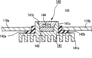
Figure 13 shows the profile of the luminescent device in the tenth preferred embodiment of the invention.
Luminescent device among the tenth embodiment is characterised in that the function of the metab described in the foregoing description and the function of metallic mirror is integrated.
Insulating part 142a, 142b have L shaped cross section, and the outer surface of tight contact reflex mirror part 141c.Although insulating part 142a, 142b are depicted as two L shaped parts, it can be the ring with L shaped cross section.Insulating part 142a, 142b are the materials that has hear resistance and insulation characterisitic as glass and pottery etc., and preferably, have the thermal coefficient of expansion of equal to go between 116a, 116b or heat sink 141.
In the operation of luminescent device 140, by submounts 143, heat sink 141 conduction are from the heat of LED element 144, and most of heat is by radiation fin 141a radiation, and other parts are by mirror portion 141c radiation.Radiation fin 141a has with the large contact surface of surrounding air long-pending, thereby carries out heat exchange effectively.
In the tenth embodiment,, do not exist therebetween and hinder thermal-radiating parts because radiation fin 141a and reflecting surface 141b are become one.Therefore, compare, can improve the thermal radiation effect of luminescent device 140 with other embodiment.In addition, because simple result can simplify production.
Outside the copper removal, heat sink 141 can be the metal that has thermal conductive resin as Al, AlN (aluminium nitride) etc.
Although in the tenth embodiment, constituted heat sink 141 by metab 111 among integrated other embodiment and metallic mirror 112, and radiation fin 141a is arranged on lower part place, alternatively, as described in other embodiment, can separating metal base 111 and metallic mirror 112, and provide radiation fin 141a to metab 111.
Figure 14 shows the luminescent device in the eleventh preferred embodiment of the invention.
The luminescent device 150 of the 11 embodiment is characterised in that by extra device and conducts most heat radiation, and in the above-described embodiments, by metab and metallic mirror or heat sink conduction heat radiation.Described extra device can be heat pipe or device with same principle.
Sheet is heat sink, and an end of 151 is positioned at the upper surface (surface of contact shoe support 113) of metab 111, and the other end is attached to radiator 152.Replace radiator 152, can use the miscellaneous parts such as casing that hold luminescent device 150.Although sheet heat sink 151 is arranged on the upper surface of metab 111, also it can be arranged on the basal surface of metab 111.
In the 11 embodiment, because sheet heat sink 151 is attached to metab 111, even when the thickness of reduction metab 111, still can strengthen radiation efficiency.The temperature that can prevent the luminescent device 150 that causes owing to long-time operation LED element 114 rises.Therefore, it is applicable to high output type.
Although the radiation fin 112a that is not provided with in the luminescent device 110 that is provided with on the metallic mirror 112 at the 7th embodiment also can not be provided with radiation fin 112a.
Figure 15 A shows the plane of the luminescent device in the twelveth preferred embodiment of the invention.Figure 15 B is the profile that obtains along the line A-A among Figure 15 A.Figure 15 C is the profile that obtains along the line B-B among Figure 15 A.
The difference of luminescent device 160 and the 7th embodiment is that lead-in wire 126 is multi-layer ceramics substrates, and is fixed in metab 121 and metallic mirror 112 by solder.
Figure 16 A shows the side view of the lead-in wire among the 12 embodiment.Figure 16 B is the profile that obtains along the line A-A among Figure 16 A.Figure 16 C is the profile that obtains along the line B-B among Figure 16 A.Figure 16 D is along the bottom view shown in the line C-C among Figure 16 A.
Lead-in wire 126 is to comprise Al
2O
3The double-deck substrate (thermal coefficient of expansion: 13.2 * 10 of glass
-6/ ℃), and have formation metal pattern 126a, 126b, 126c and 126d thereon.Pattern 126a, 126b are used for to 114 power supplies of LED element, and expose at contact portion and external terminal place to submounts 122, but most of inside by substrate.Pattern 126c, 126d also are not used in electrical connection, but are welded in metab 121 or metallic mirror 112 by solder.Solder be the Au-Si material (fusion temperature: 360 ℃, thermal coefficient of expansion: 13.9 * 10
-6/ ℃).
Therefore real lead-in wire 126a, 126b, even use conductive material anchor leg 126, can not produce short circuit by having stable on heating ceramic insulator inside yet.Ceramic member has in copper product (thermal coefficient of expansion: 16 * 10
-6/ ℃) approximately equalised thermal coefficient of expansion.Therefore, even at high temperature handle, can not produce the separation that the difference owing to thermal coefficient of expansion causes yet or break.
Although drawn anode and negative electrode,, can prevent the short circuit between pattern 126a, the 126b on substrate because circuit pattern can accurately be formed along identical direction.
In addition, when when external terminal is electrically connected, because suppressed the Al that has relatively low thermal conductivity from comprising
2O
3The heat of the pattern on glass of substrate discharges, and can easily weld.
In the above-described embodiments, luminescent coating can be arranged in the seal 118,145, so that carry out the wavelength conversion.For example, if the LED element sends blue light, luminescent coating comprises following fluorophor: Ce (cerium): YAG (yttrium-aluminium-garnet), has be subjected to when blue-light excited the characteristic of radiation gold-tinted.
In the above-described embodiments, can pass through silver-plated or aluminium, or deposit silver or aluminium, on the surface of insulated enclosure glass 117a, the 117b of the bottom that is positioned at metallic mirror 112 and submounts 113,123,143, form reflecting surface, thereby strengthen light radiation efficient.
Although in the above-described embodiments, in a seal, be provided with a LED element, the many emission types luminescent device with two and more LED elements can be provided.A plurality of LED elements of being installed can comprise the LED element of different glow colors and the LED element of identical glow color.In addition, the drive pattern of LED element can be the in parallel or series connection of all or every group of LED element.
Although seal 118,145 has smooth end face, it can have the end face as other shapes such as hemisphere.
Although in the above-described embodiments, LED element 114,144 is carried out flip-chip to be installed, but the installation that also can face up (anode, cathode electrode are arranged on upper surface and connect by lead), perhaps can install, thereby make anode, cathode electrode all be positioned at upper surface or lower surface, and be electrically connected by being directed at top electrode.Under other situations except that flip chip type, the LED element can be directly installed on metab 111,121 or heat sink 141, and need not to use submounts 113,122,143.If submounts is provided, can more reduce since LED element and metab or heat sink between the difference of thermal coefficient of expansion, the heat that produces from the LED element and the stress that causes.But the thermal radiation property of directly installing under the LED element situation is better than the situation of using submounts.
Figure 17 A shows the plane of the luminescent device in the thriteenth embodiment of the invention.Figure 17 B is the profile that obtains along the line A-A among Figure 17 A.
Submounts 212 is as Al
2O
3(aluminium oxide, thermal coefficient of expansion: 7 * 10
-6/ ℃) etc. have a material of the thermal coefficient of expansion that is approximately equal to LED element 211.The end face of submounts 212 (exposing) from support member 213 have double or less than, preferably equal the area of LED element 211.Submounts 212 has wiring layer 212a, 212b, extends to the side from end face, thereby links to each other with the electrode 211a of LED element 211.If desired, support member 213 can have the built-in Zener diode that is used to prevent dielectric breakdown.
Below, will the process of producing luminescent device 201 be made an explanation.
In discrete step, provide wiring layer 212a, 212b to submounts 212, and provide electrode 211a to LED element 211.At first, support member 213 has through hole at preposition, allows submounts 212 is inserted wherein, then, has the wiring layer 213a, the 213b that extend through through hole.Then, submounts 212 is inserted in the through hole of support member 213.At this moment, when wiring layer 212a, 212b is relative with wiring layer 213a, 213b,, be inserted into by solder (Au-Si).In this state, by under 400 ℃ or higher temperature, the solder between the fusing wiring layer is welded in support member 213 with submounts 212.Alternatively, after LED element 211 is installed in submounts 212, the submounts 212 that LED element 211 is installed on it is inserted in the support member 213.
Then, with the polarity of wiring layer 212a, 212b with when the polarity of electrode 211a is aimed at, by the Au raised pad, LED element 211 is installed on the submounts 212.Thereby, can connect and weld LED element 211.Then, utilize seal 214 to cover and sealing LED element 211 and LED element 211 near the top surface of support member 213.Although in Figure 17, seal 214 is set, have homogeneous thickness, also can be provided with, thereby on LED element 211, form the lens shaped part it.
For example, when wiring layer 213a linked to each other with the anode layer of LED element 211, the side of the positive electrode of DC power supply (not shown) linked to each other with wiring layer 213a, and negative side links to each other with wiring layer 213b.When power supply was provided, electric current flowed to wiring layer 213b from wiring layer 213a by wiring layer 212a, LED element 211 and wiring layer 212b.Thereby LED element 211 is luminous.By in the seal 214, the light that sends from the upper surface of LED element 211 to external radiation.
Obtained following effect by the 13 embodiment.
(1) because seal 214 is to the transparent glass of target wavelength, compare with sealing resin, very little by the degeneration that light and heat causes.Therefore, can obtain emission characteristics steady in a long-term.
(2) since between LED element 211 and submounts 212 balanced thermal coefficient of expansion, can reduce because the condition of high temperature when glass handled and the temperature difference between the room temperature state or because connection and close LED element 211 that the temperature difference between the LED element 211 causes and the stress of submounts 212.Therefore, can improve reliability.
(3) balanced thermal coefficient of expansion between LED element 211 and submounts 212 is made submounts 212, be inserted in the through hole of support member 213, and submounts 212 has the installation surface of the size that is approximately equal to LED element 211.Therefore, at part place with the longest air line distance in the middle of wide contact area and support member 213 and the seal 214, can reduce the stress that the condition of high temperature when glass is handled and the temperature difference between the room temperature state cause, with the generation that prevents to separate and break.
In addition, compare with seal 214, LED element 211 has the size (being approximately equal to LED element 211) that equal energy may dwindle with the submounts 212 with low thermal coefficient of expansion, and in the cooling procedure of glass, it is exerted pressure.Thereby, can prevent the generation that separates and break.Therefore, can produce the LED of glass capsulation.
(4) because seal 214 is a glass, so seal 214 can link to each other with support member 213 by chemical reaction.Therefore, compare as seal 214, can reduce the boundary separation between the two with using resin.In addition, even because between support member 213 and the seal 214 to be connected area less, still obtain enough adhesions, can the production compact package.
(5) support member 213 has the seal 214 that is positioned at the one side, and at opposite side, has wiring layer 213a, 213b, as external terminal.Therefore, can produce mini surface-mount device shape luminescent device.
(6) because parts all are heat proof materials, and reduced the stress that causes owing to variations in temperature, it is enough to bear the remelting that is applied to lead-free solder.
The glass that is used for seal 214 can be to comprise organic and hybrid glass inorganic material.This material even hear resistance, photostability and low melting point can be provided.But its thermal coefficient of expansion is greater than common employed glass, and is the same with previous described low-melting glass.
Submounts 212 can be to remove Al
2O
3Outside AlN or silicon.
Although formed through hole,,, then needn't palpiform become through hole if the exposed area of 212 pairs of seals 214 of submounts is not very big so that submounts 212 is inserted in the support member 213.
Figure 18 shows the profile to the modification of the support member of the luminescent device among the 13 embodiment.In Figure 18, only show major part, the LED mounting portion, and also not shown as other parts such as seals.
Although in the luminescent device in Figure 17 201, a LED element has been installed, a plurality of LED elements can be installed, thereby send three kinds of color R, G and B, perhaps increase the quantity of a color, to highlight or to improve color reproduction.
In this case, as shown in figure 18, the submounts 221 of luminescent device 220 has the corresponding to increase area of quantity with institute's mounted LEDs element on the Qi Ding mounting portion.In the present embodiment, three LED element 222a, 222b and 222c are installed on the submounts 221.Although submounts 221 is of different sizes, employed material is identical with submounts 212.Equally, in this case, in order to reduce stress, the mounting portion, top of submounts 221 must have can be with three LED element 222a, 222b and 222c minimum area mounted thereto.
In this structure, even when a plurality of LED element 222a, 222b and 222c are installed, still can reduce by the caused stress of thermal expansion between support member 213 and the seal (not shown), and can reduce the caused stress of thermal expansion by LED element 222a, 222b and 222c and submounts 221 places.Thus, luminescent device can have good reliability.
Figure 19 A shows the profile of the luminescent device in the fourteenth preferred embodiment of the invention.Figure 19 B shows the plane of the setting of solder layer among Figure 19 A and metal lead wire.
Although the 14 embodiment is substantially similar to the 13 embodiment, difference between the two is that its submounts is a different materials, and has different shapes, its support member 233 is to have the MULTILAYER SUBSTRATE that is formed on circuit pattern wherein, and it has the different coupling parts of support member 233 and metab 232 thereof.That is, luminescent device 230 comprises having 180Wm
-1K
-1AlN (aluminium nitride, the thermal coefficient of expansion: 5 * 10 of high thermal conductivity coefficient
-6/ ℃) submounts 231, its cross section is a convex, forms wide step portion at downside, thereby increases the contact area with metab 232.In addition, form the upper surface of metab 232, make it smooth, thereby constitute the face of weld between metab 232 and the support member 233.
Covered the seal 235 and seal 214 same materials of the presumptive area of LED element 211 and support member 233, and formed the sealing shape identical with seal 214.
The process of producing luminescent device 230 is identical with luminescent device 201, except additional metal lead-in wire 234a, 234b.Before additional metal base 232, when inserting whole parts, location metal lead wire 234a, 234b.Then, metab 232 is positioned on submounts 231 and the support member 233.In this state, enter remelting furnace,, join metal lead wire 234a, 234b and metab 232 to main body side by welding.
Conduct the electric current that puts on luminescent device 230 in the same manner with the luminescent device 201 of the 13 embodiment, still, with wiring layer 213a, the 213b among metal lead wire 234a, 234b replacement Figure 17 B.
Except the effect of the 13 embodiment, the 14 embodiment has following effect: submounts 231 has high-termal conductivity, and expansion its underpart, to widen the heat radiation path, although the installation surface of LED element 211 has and LED element 211 area identical, thereby the heat that LED element 211 produces can be conducted to metab 232, thereby, the temperature rising of 211 operating periods of LED element can be reduced, and reliability can be strengthened.
In addition, owing to, can prevent the intrusion of moisture by seal 235, support member 233 and metab 232 sealing LED elements 211 and submounts 231.
In addition, can guarantee the electric connection terminal area that is electrically connected.Can accurately aim at the height of submounts 231 and support member 233 each other.Because support member 233 is MULTILAYER SUBSTRATE, can reduce the restriction of weld metal lead-in wire 234a, 234b.
Although submounts 231 is to have 180Wm
-1K
-1The AlN of thermal conductivity factor, if thermal conductivity factor is 100Wm
-1K
-1Or bigger, then can obtain enough effects.Except that AlN, the other materials with thermal coefficient of expansion can be applied to LED element 211.
Figure 20 A shows the profile to the modification of the support member of the luminescent device among the 14 embodiment, and described support member has formation reflectance coating thereon.Figure 20 B shows the profile to another modification of support member, and described support member has the reflectance coating that is formed on its convex portion.
Although the support member 233 among Figure 19 A is kept intact its upper surface, in the present embodiment, near LED element 211, form reflectance coating, thereby strengthen the radiation efficiency of the light that sends from LED element 211.
In Figure 20 A, reflectance coating 233f is arranged on around the top of through hole 241.In Figure 20 B,, and reflectance coating 233h is set on the surface of concave portion 233g at the upside formation tapered hollow concave portion 233g of through hole 241.Can perhaps, form reflectance coating 233g, 233h by silver-colored deposit, mirror finish such as silver-plated by carrying out silver or white surface treatment.
Although in Figure 20 A, increased the thickness (highly) of submounts among Figure 19 A, can instead be support member 233 attenuation, and keep the height of the submounts 231 shown in Figure 19 A.
Above-mentioned modification except the effect of the 14 embodiment, has following effect: the free degree that can increase design submounts 231 and support member 233.
Although in Figure 20 A and 20B, an example two kinds of modifications, special-purpose speculum can be arranged on the upper surface of support member 233, be positioned at LED element 211 around.In addition, concave portion 233g can have semicircle uneven surface or diamond cutting polygon surface.
Figure 21 A shows the plane of the luminescent device in the fifteenth preferred embodiment of the invention.Figure 21 B is the profile that obtains along the line B-B among Figure 21 A.
Although the luminescent device among Figure 18 220 has a plurality of LED elements that are installed on the submounts, the luminescent device 250 of the 15 embodiment has each a plurality of LED element that all have a submounts.
Submounts 252a to 252p, support member 252 (MULTILAYER SUBSTRATE), LED element 254a to 254p and seal 255 be with submounts 212, support member 213, LED element 211 and seal 214 same materials of the 13 embodiment, have identical characteristic (thermal coefficient of expansion etc.).Copper foil layer 258 is arranged on submounts 252a (surfaces of metab 251 sides) to the basal surface of 252p and support member 235, so that it is welded on the metab 251.Submounts 252a is referred to as Copper Foil 258 to the Copper Foil of 252p and support member 253.
Another utmost point (as negative electrode) of first to the 4th group connects terminals 256a each in the 256d respectively, terminals 256a links to each other to the end of R4 with current-limiting resistance R1 to 256d, and the other end of resistance R 1 to R4 links to each other to 257d with the terminals 257a that is used to power.Resistance R 1 to R4 is not arranged on submounts 252a in 252p or support member 253, but external mounting.For example, when applying the DC power supply with predetermined voltage between terminals 257a and terminals 256e, four LED element 254a are simultaneously luminous to 254d.When applying power supply between terminals 256a, 257d and terminals 256e, eight LED element 254a are simultaneously luminous to 254p to 254d and 254m.
By the 15 embodiment, obtained following effect.
(1) except the effect of the 14 embodiment, because luminescent device 250 provides submounts to each LED element, even when increasing or reducing the quantity of employed LED element, still can reduce at LED element 254a and rise to the temperature of the operated device of 254p.In addition, when changing the quantity of LED element, do not need to redesign submounts.Therefore, the flexibility of design can be strengthened, and the time of delivery of customer order can be shortened.
(2) because seal 255 has the thermal coefficient of expansion that is approximately equal to support member 253, and similar island is such, submounts 252a is arranged in the support member 253 to 252p, can move each submounts neatly according to having thermal expansion or the contraction to the seal 255 and the support member 253 of the thermal coefficient of expansion of 252p greater than submounts 252a.Therefore, even when a plurality of LED element is set, the stress that causes owing to temperature still is equal to the situation of single led element.Stress between LED element and the submounts can not take place.In addition, the boundary separation between seal 255 and the support member 253 can not take place.
(3) since by submounts 252a to 252p to support member 253 radiation by LED element 254a to the heat that 254p produced, can strengthen radiation efficiency.Even when LED254a when 254p is high performance type, LED254a to 254p, submounts 252a to 252p, support member 253, seal 254 etc. can not be subjected to fire damage.Therefore, can strengthen hear resistance, weatherability and durability.
(4) because use MULTILAYER SUBSTRATE, can form any circuit pattern, and need not to disturb thermal radiation property as support member 253.
Figure 22 A shows the plane of the luminescent device in the sixteenth preferred embodiment of the invention.Figure 22 B is the profile that obtains along the line C-C among Figure 22 A.
The luminescent device 260 of the 16 embodiment is identical with luminescent device 250 among Figure 21 A and Figure 21 B basically.Difference is, comprises Al with promptly being arranged on as the metallic mirror 261 of speculum again as second radiator
2O
3The support member 253 of glass on.Similar parts are represented with employed same numbers in the luminescent device 250 among Figure 21 A and Figure 21 B.In Figure 22 A and 22B, not shown metab.
By 900 ℃ heat treatment,, metallic mirror 261 is welded on the support member 253 through peroxidating.On 16 reflecting surface 261a and metallic mirror 261, form seal 262 with predetermined altitude.Seal 262 be with last embodiment in seal 214 same materials, and have an identical attribute (thermal coefficient of expansion etc.).
Except the effect of the 13 to the 15 embodiment, obtain following effect by the 16 embodiment.
(1) has the metallic mirror 261 to corresponding 16 the reflecting surface 261a of 254p owing on support member 253, being provided with LED element 254a, can effectively take out the light that sends to 254p from LED element 254a along required direction according to the shape of reflecting surface 261a.
(2) because seal 262 has the thermal coefficient of expansion that is approximately equal to support member 253 and metallic mirror 261, even when between seal 262 and support member 253, metallic mirror 261 being set, the stress that produces owing to temperature can not take place yet, and boundary separation etc. can not take place.
Figure 23 shows the profile to the modification of the support member among the 16 embodiment.In Figure 23, only show near the LED element 254i, and not shown other parts.
Thereby, by forming wiring layer 273 as the radiation path, the heat that can easily produce by LED element 254i to metallic mirror 261 conduction by copper foil layer 274, metab (not shown), copper foil layer 271, wiring layer 273 and copper foil layer 276 from submounts 252i.Thus, can strengthen thermal radiation property.
Figure 24 A shows the profile of the luminescent device in the seventeenth embodiment of the invention.Figure 24 B shows the profile to the modification of the luminescent device among Figure 24 A.
The luminescent device 280 of the 17 embodiment is characterised in that, sheet metal, conductor is used as support member, and in the aforementioned embodiment, insulating materials is used as support member.
Below, will the process of producing luminescent device 280 be made an explanation.
At first, submounts 282 is inserted the through hole of sheet metal 283 from the bottom side of Figure 24 A.Then, at the top surface of submounts 282 LED element 281 is installed.Then, it is sealed, can produce luminescent device 280 by utilizing seal 284.
Alternatively, on the top surface that LED element 281 is installed in submounts 282 after, submounts 282 is inserted in the through hole of sheet metals 283.Speculum can be arranged on the surface of sheet metal 283.
Except the 13 and the effect of the 14 embodiment, the 17 embodiment has following effect: sheet metal 283 is as radiator, simultaneously as the support member that supports submounts 282.Therefore, can obtain specific radiation effect, and need not to use metab.Therefore, luminescent device can be low section.
As mentioned above, even in the structure shown in Figure 24 A, still can obtain specific radiation effect by sheet metal 283.But,, shown in Figure 24 B, can increase the metab of copper or aluminium if want to increase radiation characteristic.Shown in Figure 24 B, can be arranged on the welding of the solder layer 282g on the basal surface of submounts 282 by use, metab 287 is appended on the basal surface of submounts 282.Below sheet metal 283, polyimide substrate 286 (dielectric substrate) is set.Polyimide substrate 286 has the inside wiring layer (not shown) that links to each other with electrode 282c, 282d.
Figure 25 A shows the profile to another modification of the luminescent device among Figure 24 A.Figure 25 B shows the bottom view of the submounts among Figure 25 A.
Therefore, between polyimide substrate 286 and submounts 282, provide simple distribution.In addition, the opposite side that do not link to each other with polyimide substrate 286 of submounts 282 can be as the radiation path of going to metab 287.Therefore, it can have good heat extraction attribute.
Figure 26 shows the profile to another modification of the luminescent device among Figure 24 A.In Figure 26, similar parts are represented with employed same numbers among Figure 24 A.
The material of seal 284 is not limited to low-melting glass, can be epoxy resin or silicones.Resin can not be similar to low-melting glass and have the thermal coefficient of expansion identical with metal like that, and in fact, it has the thermal coefficient of expansion times over metal.But, because the treatment temperature of resin is lower than low-melting glass, and not having low heat conductivity as submounts as the sheet metal 291 of support member, the amount of thermal expansion is not very big.Therefore, can prevent separation or broken.
Except the effect of the 16 embodiment, the 17 embodiment has following effect: because sheet metal 291 has reflecting surface 291b, can strengthen light extraction efficiency.In addition,, can reduce radiation resistance as radiator because increased the thickness of sheet metal 291, thus can enhanced rad efficient.
Figure 27 shows the profile of the luminescent device in the eighteenth embodiment of the invention.
The 18 embodiment is characterised in that, used the face up type LED element that will link to each other with the current feed side by lead, and in the above-described embodiments, used face down type LED element.
Although in Figure 27, submounts 302 is much wideer than LED element 301 from the expose portion of support member 303, in fact, only need be wideer a little, so that the wire bonds space is provided.Required is, and expose portion has is the twice of LED element 301 or littler area.If first seal 305 is elastomeric material or the buffering effect parts with the thermal coefficient of expansion between the submounts 302 and second seal 306, expose portion can be wide slightly.
Below, will the process of producing luminescent device 300 be made an explanation.
At first, from the bottom side of Figure 27, submounts 302 is inserted in the through hole that is formed on the precalculated position.Submounts 302 has formation wiring layer 302a, 302b thereon.Then, with LED element 301,, be installed on the submounts 302 at preposition.Then, by lead 304a, 304b, the top electrode (not shown) of LED element 301 is welded on wiring layer 302a, the 302b.First seal, 305 sealing LED elements 301 cover lead 304a, 304b simultaneously.In addition, the surface and the support member 303 of second seal, 306 sealings, first seal 305.
In the 18 embodiment,, in sealing, can guardwire 304a, 304b not be stressed, thereby can not be out of shape or rupture because used double seal.Therefore, even when use faces up LED element 301, also can obtain and the described identical effect of the foregoing description.
Figure 28 shows the profile of the luminescent device in the nineteenth embodiment of the invention.
The difference of the luminescent device 310 of present embodiment and the luminescent device 300 of the 18 embodiment is that first seal 305 is the silicones as elastomeric material, has used (flip-chip) type element that faces down, and has used another kind of production process.Similar parts are represented with employed same numbers among Figure 27.
When producing luminescent device 310, at first, support member 303 is put into platinum mould with glass contact surface.This mould have with submounts 302 is inserted wherein the corresponding to shape of convex-concave and from the outstanding part of the upper surface of support member 303, form the corresponding to hemispherical of face 306b with the element spatial accommodation.Then,, weld second seal 306, and form lens surface 306a and element spatial accommodation formation face 306b by the heating low-melting glass.Then, the silicones injection element spatial accommodation that forms first seal 305 is formed in the element spatial accommodation of face 306b inside, then, make its sclerosis.Then, LED element 301 is installed on the submounts 302.Then, with the bottom of submounts 302, insert in the through hole of the pre-position that is formed on support member 303, and utilize solder, welding support member 303 and submounts 302 from Figure 28.In this case, silicones has elasticity, therefore, when being pressed into LED element 301 wherein, can deform according to the surface configuration of LED element 301, thus sealing LED element 301.When welding submounts 302, can use other scolders except that solder.
Obtained following effect by the 19 embodiment.
(1) by metab being appended to the bottom side among Figure 28, it is such to be similar to the 14 embodiment, prevents the intrusion of moisture etc.
(2) because when handling glass, LED element 301 does not expose and hot environment, even can use the LED element 301 with low heat resistant.Except low-melting glass, can use glass with higher melt.
(3) owing to second seal 306 with glass material covers first seal 305, can keep the shape of lens surface 306a.The pure silicon resin is because heat or light are degenerated a little, but the additive that is used to harden makes its decolouring.In the 19 embodiment,, can prevent because the decline that the light that the degeneration that heat or light cause causes is exported by using the pure silicon resinon as first seal 305.Thereby, can strengthen reliability.
In luminescent device 201,230,250,260,280,285,290,300 and 310, the luminescent coating that is used for the wavelength conversion can be arranged on the glass capsulation part.For example, when the LED element sent blue light, luminescent coating can be to have at the fluorophor that is subjected to giving off when blue-light excited the characteristic of gold-tinted as Ce (cerium): YAG (yttrium-aluminium-garnet) etc.
In the above-described embodiments, can metab 215,232,251 and 287, sheet metal 283 and 289 and metallic mirror 261 on form radiation fin, perhaps additional thereon.Thereby, can further strengthen radiation efficiency.
Although seal 214,235 is formed smooth, also can form it into lamp shape, diamond cutting etc.
In addition, the present invention is not limited to luminescent device, can be applied to as the luminescent device of uses such as semiconductor devices as light receiving elements such as solar cells.Because seal is a glass, even long-time the exposure in the sun can not degenerated yet.Can provide as luminescent devices such as solar cells, have convergent lens and small light receiving element.By using the present invention, can prevent because the decline of the conversion efficiency that the temperature rising causes, and can strengthen weatherability and hear resistance.
Although in the above-described embodiments, the flip chip type element uses Au button shape pad, and pad also can be the other materials except that Au, perhaps can replace with the contact except that pad.
Although for complete and clearly open, with reference to specific embodiment, invention has been described, thereby to claims do not limited, but be appreciated that specific implementation those of ordinary skill in the art thinkable, fall into all modifications and optional structure among the basic religious doctrine described here.
Claims (12)
1. luminescent device comprises:
Light-emitting component sends the light of predetermined wavelength; And
Hermetic unit, the sealed light emitting element,
Wherein said light-emitting component has stress and reduces part, reduces the internal stress in the hermetic unit,
Described stress reduces the dihedral one-tenth of part by the light-emitting component of cutting sth. askew,
Described hermetic unit is a glass, and
Described light-emitting component is a flip chip type.
2. luminescent device according to claim 1 is characterized in that:
Described light-emitting component comprises that refractive index equals the substrate of the luminescent layer of light-emitting component.
3. luminescent device according to claim 1 is characterized in that:
Described substrate comprises GaN or SiC.
4. luminescent device according to claim 1 is characterized in that:
Described hermetic unit has along the optic shape of predetermined direction radiant light.
5. luminescent device according to claim 1 is characterized in that:
Have at least two compound glasses that laminate glassy layer by hot pressing, the formation that is integrated of described hermetic unit.
6. luminescent device according to claim 5 is characterized in that:
Described compound glass comprises at least between described two glassy layers, by light activated thin film phosphor layers.
7. luminescent device according to claim 5 is characterized in that:
Described compound glass comprises the glassy layer that comprises fluorescent complex, to comprise by light activated fluorescent complex.
8. method that is used to make luminescent device comprises:
In the upside-down mounting mode light-emitting component is installed on the base;
On base and below glass is set; And
Hot pressing glass on base and light-emitting component, with the sealed light emitting element and on light-emitting component, form hermetic unit,
Wherein said light-emitting component has stress and reduces part, reduces the internal stress in the hermetic unit, and
Described stress reduces the dihedral one-tenth of part by the light-emitting component of cutting sth. askew.
9. method according to claim 8, wherein
Described glass is plate-like.
10. method according to claim 8, wherein
Described glass is softening to 10
8To 10
10Carry out hot pressing in the time of pool.
11. method according to claim 8, wherein
Described base comprises ceramic substrate.
12. method according to claim 8 also comprises:
By cutting, remove unnecessary glass from the light-emitting component of sealing.
Applications Claiming Priority (9)
| Application Number | Priority Date | Filing Date | Title |
|---|---|---|---|
| JP2003276099 | 2003-07-17 | ||
| JP2003-276099 | 2003-07-17 | ||
| JP2003276099A JP4238666B2 (en) | 2003-07-17 | 2003-07-17 | Method for manufacturing light emitting device |
| JP2003-353007 | 2003-10-10 | ||
| JP2003353007A JP4254470B2 (en) | 2003-10-10 | 2003-10-10 | Light emitting device |
| JP2003353007 | 2003-10-10 | ||
| JP2003-358308 | 2003-10-17 | ||
| JP2003358308 | 2003-10-17 | ||
| JP2003358308A JP4238693B2 (en) | 2003-10-17 | 2003-10-17 | Optical device |
Related Parent Applications (1)
| Application Number | Title | Priority Date | Filing Date |
|---|---|---|---|
| CNB2004100712619A Division CN100472820C (en) | 2003-07-17 | 2004-07-16 | Illuminating device |
Publications (2)
| Publication Number | Publication Date |
|---|---|
| CN101476710A CN101476710A (en) | 2009-07-08 |
| CN101476710B true CN101476710B (en) | 2011-01-05 |
Family
ID=34212528
Family Applications (1)
| Application Number | Title | Priority Date | Filing Date |
|---|---|---|---|
| CN2009100096747A Expired - Fee Related CN101476710B (en) | 2003-07-17 | 2004-07-16 | Illuminating device and its manufacture method |
Country Status (2)
| Country | Link |
|---|---|
| JP (1) | JP4238666B2 (en) |
| CN (1) | CN101476710B (en) |
Families Citing this family (13)
| Publication number | Priority date | Publication date | Assignee | Title |
|---|---|---|---|---|
| WO2006112417A1 (en) * | 2005-04-15 | 2006-10-26 | Asahi Glass Company, Limited | Glass-sealed light-emitting device, circuit board with glass-sealed light-emitting device, and methods for manufacturing those |
| JP4604819B2 (en) * | 2005-04-28 | 2011-01-05 | 豊田合成株式会社 | Light emitting device |
| JP2007201354A (en) * | 2006-01-30 | 2007-08-09 | Matsushita Electric Ind Co Ltd | Light-emitting module |
| JP2007258466A (en) * | 2006-03-23 | 2007-10-04 | Sumita Optical Glass Inc | Illuminating device, and light-emitting device |
| DE102008021436A1 (en) * | 2008-04-29 | 2010-05-20 | Schott Ag | Optic converter system for (W) LEDs |
| US9634203B2 (en) * | 2008-05-30 | 2017-04-25 | Sharp Kabushiki Kaisha | Light emitting device, surface light source, liquid crystal display device, and method for manufacturing light emitting device |
| WO2011007816A1 (en) * | 2009-07-15 | 2011-01-20 | 三菱化学株式会社 | Semiconductor light-emitting element, semiconductor light-emitting device, method for manufacturing semiconductor light-emitting element, and method for manufacturing semiconductor light-emitting device |
| JP2013077798A (en) * | 2011-09-14 | 2013-04-25 | Toyoda Gosei Co Ltd | Glass sealing led lamp and manufacturing method of the same |
| JP5880025B2 (en) * | 2011-12-26 | 2016-03-08 | 日亜化学工業株式会社 | Light emitting device |
| KR102059030B1 (en) * | 2012-09-24 | 2019-12-24 | 엘지이노텍 주식회사 | Ultraviolet light emitting device |
| JP2015079929A (en) | 2013-09-11 | 2015-04-23 | 株式会社東芝 | Semiconductor light-emitting device and method of manufacturing the same |
| JP6477734B2 (en) * | 2016-06-30 | 2019-03-06 | 日亜化学工業株式会社 | Light emitting device and manufacturing method thereof |
| CN110118312A (en) * | 2018-02-07 | 2019-08-13 | 深圳光峰科技股份有限公司 | Wavelength converter |
Citations (2)
| Publication number | Priority date | Publication date | Assignee | Title |
|---|---|---|---|---|
| US5937273A (en) * | 1994-12-27 | 1999-08-10 | Fujitsu Limited | Fabricating compound semiconductor by varying ratio of stagnant layer thickness and mean free path of seed material |
| JP2001185757A (en) * | 1999-12-27 | 2001-07-06 | Toyoda Gosei Co Ltd | Group iii nitride based compound semiconductor light emitting element |
Family Cites Families (13)
| Publication number | Priority date | Publication date | Assignee | Title |
|---|---|---|---|---|
| JPS5995652U (en) * | 1982-12-18 | 1984-06-28 | 株式会社東芝 | light emitting element |
| EP0405757A3 (en) * | 1989-06-27 | 1991-01-30 | Hewlett-Packard Company | High efficiency light-emitting diode |
| JP2979961B2 (en) * | 1994-06-14 | 1999-11-22 | 日亜化学工業株式会社 | Full color LED display |
| DE29724582U1 (en) * | 1996-06-26 | 2002-07-04 | Osram Opto Semiconductors Gmbh | Light-emitting semiconductor component with luminescence conversion element |
| JPH1140871A (en) * | 1997-07-22 | 1999-02-12 | Mitsubishi Chem Corp | Photoelectric conversion element |
| JP2861991B2 (en) * | 1997-10-20 | 1999-02-24 | 日亜化学工業株式会社 | Method of manufacturing gallium nitride based compound semiconductor chip |
| JP3449201B2 (en) * | 1997-11-28 | 2003-09-22 | 日亜化学工業株式会社 | Method for manufacturing nitride semiconductor device |
| JP3707279B2 (en) * | 1998-03-02 | 2005-10-19 | 松下電器産業株式会社 | Semiconductor light emitting device |
| JP3337000B2 (en) * | 1999-06-07 | 2002-10-21 | サンケン電気株式会社 | Semiconductor light emitting device |
| JP2001144331A (en) * | 1999-09-02 | 2001-05-25 | Toyoda Gosei Co Ltd | Light-emitting device |
| JP3989794B2 (en) * | 2001-08-09 | 2007-10-10 | 松下電器産業株式会社 | LED illumination device and LED illumination light source |
| JP2003147346A (en) * | 2001-11-15 | 2003-05-21 | Kansai Tlo Kk | Photo-functional material made by using rare earth element complex, and light emitting device |
| JP2003188410A (en) * | 2001-12-19 | 2003-07-04 | Daido Steel Co Ltd | Light emitting diode chip |
-
2003
- 2003-07-17 JP JP2003276099A patent/JP4238666B2/en not_active Expired - Fee Related
-
2004
- 2004-07-16 CN CN2009100096747A patent/CN101476710B/en not_active Expired - Fee Related
Patent Citations (2)
| Publication number | Priority date | Publication date | Assignee | Title |
|---|---|---|---|---|
| US5937273A (en) * | 1994-12-27 | 1999-08-10 | Fujitsu Limited | Fabricating compound semiconductor by varying ratio of stagnant layer thickness and mean free path of seed material |
| JP2001185757A (en) * | 1999-12-27 | 2001-07-06 | Toyoda Gosei Co Ltd | Group iii nitride based compound semiconductor light emitting element |
Also Published As
| Publication number | Publication date |
|---|---|
| JP4238666B2 (en) | 2009-03-18 |
| CN101476710A (en) | 2009-07-08 |
| JP2005039122A (en) | 2005-02-10 |
Similar Documents
| Publication | Publication Date | Title |
|---|---|---|
| CN100472820C (en) | Illuminating device | |
| JP3976063B2 (en) | Light emitting device | |
| US9653663B2 (en) | Ceramic LED package | |
| JP4192742B2 (en) | Light emitting device | |
| JP4303550B2 (en) | Light emitting device | |
| JP5197874B2 (en) | Light emitting module, light source device, liquid crystal display device, and method for manufacturing light emitting module | |
| CN100565948C (en) | Light-emitting device | |
| US7670872B2 (en) | Method of manufacturing ceramic LED packages | |
| CN101740560B (en) | Light-emitting apparatus, backlight apparatus, and display apparatus | |
| CN101476710B (en) | Illuminating device and its manufacture method | |
| TW200828635A (en) | Light emitting device, its manufacturing method and its mounted substrate | |
| CN113394654A (en) | Laser device | |
| JP5126127B2 (en) | Method for manufacturing light emitting device | |
| JP4010340B2 (en) | Light emitting device | |
| JP4016925B2 (en) | Light emitting device | |
| CN211654852U (en) | Light emitting device and carrier | |
| CN215988749U (en) | High-power LED light source | |
| JP4165610B2 (en) | Method for manufacturing light emitting device | |
| CN111180567A (en) | Carrier and light emitting device | |
| KR101055673B1 (en) | LED module using metal substrate and manufacturing method thereof | |
| JP4737218B2 (en) | Method for manufacturing light emitting device |
Legal Events
| Date | Code | Title | Description |
|---|---|---|---|
| C06 | Publication | ||
| PB01 | Publication | ||
| C10 | Entry into substantive examination | ||
| SE01 | Entry into force of request for substantive examination | ||
| C14 | Grant of patent or utility model | ||
| GR01 | Patent grant | ||
| CF01 | Termination of patent right due to non-payment of annual fee |
Granted publication date: 20110105 Termination date: 20210716 |
|
| CF01 | Termination of patent right due to non-payment of annual fee |