CN100542055C - The timing adjusting method of transtation mission circuit, radio communication device and transtation mission circuit - Google Patents

The timing adjusting method of transtation mission circuit, radio communication device and transtation mission circuit Download PDF

Info

Publication number
CN100542055C
CN100542055C CNB200410081805XA CN200410081805A CN100542055C CN 100542055 C CN100542055 C CN 100542055C CN B200410081805X A CNB200410081805X A CN B200410081805XA CN 200410081805 A CN200410081805 A CN 200410081805A CN 100542055 C CN100542055 C CN 100542055C
Authority
CN
China
Prior art keywords
mentioned
signal
circuit
digital
analog
Prior art date
Legal status (The legal status is an assumption and is not a legal conclusion. Google has not performed a legal analysis and makes no representation as to the accuracy of the status listed.)
Expired - Fee Related
Application number
CNB200410081805XA
Other languages
Chinese (zh)
Other versions
CN1642025A (en
Inventor
鈴木芽衣
堀一行
矢野隆
Current Assignee (The listed assignees may be inaccurate. Google has not performed a legal analysis and makes no representation or warranty as to the accuracy of the list.)
Hitachi Ltd
Original Assignee
Hitachi Communication Technologies Ltd
Priority date (The priority date is an assumption and is not a legal conclusion. Google has not performed a legal analysis and makes no representation as to the accuracy of the date listed.)
Filing date
Publication date
Application filed by Hitachi Communication Technologies Ltd filed Critical Hitachi Communication Technologies Ltd
Publication of CN1642025A publication Critical patent/CN1642025A/en
Application granted granted Critical
Publication of CN100542055C publication Critical patent/CN100542055C/en
Expired - Fee Related legal-status Critical Current
Anticipated expiration legal-status Critical

Links

Images

Classifications

    • HELECTRICITY
    • H04ELECTRIC COMMUNICATION TECHNIQUE
    • H04BTRANSMISSION
    • H04B1/00Details of transmission systems, not covered by a single one of groups H04B3/00 - H04B13/00; Details of transmission systems not characterised by the medium used for transmission
    • H04B1/02Transmitters
    • H04B1/04Circuits
    • H04B1/0475Circuits with means for limiting noise, interference or distortion
    • HELECTRICITY
    • H04ELECTRIC COMMUNICATION TECHNIQUE
    • H04BTRANSMISSION
    • H04B1/00Details of transmission systems, not covered by a single one of groups H04B3/00 - H04B13/00; Details of transmission systems not characterised by the medium used for transmission
    • H04B1/02Transmitters
    • H04B1/04Circuits
    • HELECTRICITY
    • H03ELECTRONIC CIRCUITRY
    • H03FAMPLIFIERS
    • H03F1/00Details of amplifiers with only discharge tubes, only semiconductor devices or only unspecified devices as amplifying elements
    • H03F1/32Modifications of amplifiers to reduce non-linear distortion
    • H03F1/3241Modifications of amplifiers to reduce non-linear distortion using predistortion circuits
    • H03F1/3247Modifications of amplifiers to reduce non-linear distortion using predistortion circuits using feedback acting on predistortion circuits
    • HELECTRICITY
    • H03ELECTRONIC CIRCUITRY
    • H03FAMPLIFIERS
    • H03F1/00Details of amplifiers with only discharge tubes, only semiconductor devices or only unspecified devices as amplifying elements
    • H03F1/32Modifications of amplifiers to reduce non-linear distortion
    • H03F1/3241Modifications of amplifiers to reduce non-linear distortion using predistortion circuits
    • H03F1/3282Acting on the phase and the amplitude of the input signal
    • HELECTRICITY
    • H03ELECTRONIC CIRCUITRY
    • H03FAMPLIFIERS
    • H03F1/00Details of amplifiers with only discharge tubes, only semiconductor devices or only unspecified devices as amplifying elements
    • H03F1/34Negative-feedback-circuit arrangements with or without positive feedback
    • HELECTRICITY
    • H03ELECTRONIC CIRCUITRY
    • H03FAMPLIFIERS
    • H03F3/00Amplifiers with only discharge tubes or only semiconductor devices as amplifying elements
    • H03F3/189High frequency amplifiers, e.g. radio frequency amplifiers
    • HELECTRICITY
    • H03ELECTRONIC CIRCUITRY
    • H03FAMPLIFIERS
    • H03F3/00Amplifiers with only discharge tubes or only semiconductor devices as amplifying elements
    • H03F3/20Power amplifiers, e.g. Class B amplifiers, Class C amplifiers
    • H03F3/24Power amplifiers, e.g. Class B amplifiers, Class C amplifiers of transmitter output stages
    • HELECTRICITY
    • H04ELECTRIC COMMUNICATION TECHNIQUE
    • H04BTRANSMISSION
    • H04B1/00Details of transmission systems, not covered by a single one of groups H04B3/00 - H04B13/00; Details of transmission systems not characterised by the medium used for transmission
    • H04B1/02Transmitters
    • H04B1/04Circuits
    • H04B1/0483Transmitters with multiple parallel paths
    • HELECTRICITY
    • H04ELECTRIC COMMUNICATION TECHNIQUE
    • H04LTRANSMISSION OF DIGITAL INFORMATION, e.g. TELEGRAPHIC COMMUNICATION
    • H04L27/00Modulated-carrier systems
    • HELECTRICITY
    • H04ELECTRIC COMMUNICATION TECHNIQUE
    • H04LTRANSMISSION OF DIGITAL INFORMATION, e.g. TELEGRAPHIC COMMUNICATION
    • H04L7/00Arrangements for synchronising receiver with transmitter
    • H04L7/0054Detection of the synchronisation error by features other than the received signal transition
    • HELECTRICITY
    • H04ELECTRIC COMMUNICATION TECHNIQUE
    • H04LTRANSMISSION OF DIGITAL INFORMATION, e.g. TELEGRAPHIC COMMUNICATION
    • H04L7/00Arrangements for synchronising receiver with transmitter
    • H04L7/02Speed or phase control by the received code signals, the signals containing no special synchronisation information
    • HELECTRICITY
    • H03ELECTRONIC CIRCUITRY
    • H03FAMPLIFIERS
    • H03F2200/00Indexing scheme relating to amplifiers
    • H03F2200/451Indexing scheme relating to amplifiers the amplifier being a radio frequency amplifier
    • HELECTRICITY
    • H04ELECTRIC COMMUNICATION TECHNIQUE
    • H04BTRANSMISSION
    • H04B1/00Details of transmission systems, not covered by a single one of groups H04B3/00 - H04B13/00; Details of transmission systems not characterised by the medium used for transmission
    • H04B1/02Transmitters
    • H04B1/04Circuits
    • H04B2001/0408Circuits with power amplifiers
    • H04B2001/0433Circuits with power amplifiers with linearisation using feedback

Abstract

The invention provides a kind of timing adjusting method of radio communication device.In radio communication device, the r signal of the I signal of adjustment such as quadrature modulation mode and Q signal, EER mode is poor with the delay of two signal paths that are synthesized after the θ signal is modulated by the path with different retardations like that, improves the linear property that sends signal thus.It has: the DA translation circuit, and combiner circuit, distributor circuit, the AD translation circuit, oscillating circuit, first split circuit and comparison circuit, wherein, above-mentioned oscillating circuit is controlled its output according to the comparative result by means of comparison circuit.

Description

The timing adjusting method of transtation mission circuit, radio communication device and transtation mission circuit
Technical field
The present invention relates to a kind of transmitter-receiver of adjusting the function of the timing that sends signal by means of the FEEDBACK CONTROL of closed loop that has, particularly a kind of employing EER mode is adjusted the transmission transmitter-receiver regularly of r (amplitude) composition and θ (phase place) composition.
Background technology
In sender with base station headed by the portable phone, that be equipped on wireless communication system and terminal, developed become two systems to carry out respectively handling the transmission Signal Separation after, synthetic once more and send the method for output.As this method, known for example have, and becomes the method that I signal and Q signal handle or be separated into r (amplitude) composition and EER (Envelope Elimination andRestoration) mode that θ (phase place) composition is handled sending Signal Separation.
But, separate the signal under the situation that two systems handle this, if in the configuration of treatment circuit, the signal path lengths of each treatment system there are differences then will produce difference on the signal transmission delay time.In addition, if each Signal Processing circuit difference of being separated then on signal processing time, will produce difference.Thus, the timing when signal is carried out synthesizing once more will misplace, and signal quality will deterioration.
Particularly the EER mode is carried out synthetic (non-patent literature 1) once more with the higher saturation type power amplifier of efficient (Power Amplifier) after carrying out frequency translation to r signal enforcement supply voltage modulation and to the θ signal.Because in the communicator overall electric power consumes, the ratio shared to the power consumption that sends the power amplifier that signal amplifies is very big, so that the high efficiency of power amplifier just becomes technical task.Because the EER mode has been used the power amplifier of the higher saturation type of efficient, so it is believed to solve miniaturization, cost degradation and the low power consumptionization that this problem also can realize communicator.
But the EER mode exists the defective that is easy to generate difference on the retardation.The supply voltage modulation circuit of r composition side is by such as DC-DC converter formations such as (DC-DC converters), relative therewith, the frequency-conversion circuit of θ data side is by constituting such as frequency mixer etc., because the circuit element that uses exists than big-difference separately, so the timing the when delay that is produced in the process of signal processing just makes once more composite signal dislocation, and make the remarkable deterioration of signal quality.
Fig. 7 is that the delay that is illustrated in r signal and θ signal in the EER mode makes the oscillogram of the principle that sends the signal quality deterioration.
If sine wave is input in the sender of EER mode, then amplitude ingredient r (θ) 101 becomes along the x axle and turns back in the waveform of sine wave, and phase component p (θ) 102 becomes square wave.Originally, the phasing back of turning back regularly with p (θ) 102 of r (θ) 101 should be synchronous regularly, still, considered the situation of the corresponding τ that lagged behind of timing of p (θ) 102.At this moment, both are carried out signal S (θ) 103 after synthetic again, phase place is corresponding reverses during τ discontinuously, and produces sharp-pointed crest in rub-out signal u (θ) 104.This rub-out signal becomes to be divided into output parasitic signal (noise signal) and makes the signal quality deterioration, so in order to obtain desirable signal quality, need take someway the delay difference of r signal and θ signal to be adjusted so that both timings are consistent.
Fig. 8 is the block diagram of timing adjusting method in the past of the transmitter-receiver of explanation EER mode.In Fig. 8, the less side of the delay that causes among r signal path 201 and θ signal path 202, because of circuit element (at this moment, suppose Δ dr>Δ d θ, the θ side) the path in insert the delay Δ dd be equivalent to postpone difference Δ dr-Δ d θ so that the retardation unanimity in two paths.In Fig. 8, in numeric area, insert Δ dd, if Δ dd is the integral multiple of clock cycle, then can by utilize shift-register circuit 203 grades merely phase delay n clock adjust.
But, usually, delay also taking place, because of the external cause of variations in temperature etc. changes in time with the tiny unit of less than 1 clock.In non-patent literature 1, proposed following method, that is: by means of to sending the digital filter that signal carries out linear interpolation, adjusted postponing with the precision of 1/2 clock.As shown in Figure 8, the digital-to-analog converter in two paths (DAC) 204,205 is driven by single master clock source 206 (fixed-frequency) in this structure.
Then, the example of having used the timing adjusting method of feedback (Fb) circuit in the transmitter-receiver of the mode beyond the EER is described.
Fig. 9 is illustrated in the sender of predistortion (distortion compensation) mode, adjusts the block diagram (with reference to patent documentation 1) of the method for the timing that sends signal and feedback signal.
In Fig. 9, feedback circuit 301 receives the signal after being amplified by power amplifier (PA) 302, and compares with original transmission signal, is determined at the amount of the nonlinear distortion that produces in the transmission signal path 303 that comprises power amplifier 302 thus.Then, distortion compensation coefficient operational part 304 is obtained the coefficient of the distortion that is used to provide the opposite characteristic of eliminating this nonlinear distortion, and is set in predistortion portion 305.Predistortion portion 305 provides nonlinear distortion in conjunction with the coefficient that sets to sending signal, and is sent to frequency-conversion circuit 307 by DAC306.
On the other hand, time of delay, determination section 308, and the timing when relatively sending signal with feedback signal in order to make is consistent, and it is poor to detect both delay, with the retardation of decision shift-register circuit 309 (Δ d1) and variable delay element 310 (Δ d2).Δ d1309 is according to the feasible constant time lag that sends signal of the integral multiple of clock cycle, and Δ d2310 is with the feasible phase delay that feedback signal is transformed to the analog-to-digital converter (ADC) 311 of digital signal of 1/n clock-unit.In addition, in this structure, DAC306 is driven by the master clock source identical with the master clock source that drives ADC311, and its clock phase is fixed.
(non-patent literature 1) Je-Kuan Jau, " Linear Interpolation Scheme forCompensation of Path-Delay Difference in an Envelope Eliminationand Restoration Transmitter ", pp1072-1075, Proceedings of APMC2001.
(patent documentation 1) Japanese Patent Application Publication spy opens the 2001-189685 communique
If adopt method shown in Figure 8, then also can adjust the delay that is taken place with less than 1 clock-unit, but, there is such problem, that is: because adjustment amount is discontinuous, so on the basis of remaining quantization error, be subjected to the influence of the group delay frequency characteristic of filter in adjustment amount, retardation makes the signal quality deterioration because of deviation takes place for the difference of frequency.Though, also can in simulated domain, insert Δ dd by delay line, owing to be difficult to make exactly retardation to take place, because of the characteristic deviation of the analog element that external cause caused of variations in temperature etc. is bigger, so performance is bad.In addition, if the retardation of being inserted is changed discontinuously, then will send the discontinuous variation of generation on the signal waveform, and worry the deterioration of the parasitic output characteristic of transmission signal in its moment.
In method shown in Figure 9, with method shown in Figure 8 similarly, remaining quantization error in retardation.In addition, this is to be used to make the consistent function of timing that sends signal and feedback signal, owing to do not possess the function that the delay difference between 2 compositions that send signal is adjusted, so can't solve the problem of above-mentioned EER mode.
Summary of the invention
The present invention finishes in view of the above problems, its purpose be to provide a kind of in the transmitter-receiver of EER mode with simple circuit and adjust the r signal accurately and the method for the delay difference of θ signal.In addition, even its purpose also is to provide a kind of method of being modulated the delay difference of two signal paths that synthesized once more the back such as I signal and Q signal like that by the path with different retardations of also adjusting in the transmitter-receiver beyond the EER mode.
Technical scheme of the present invention provides a kind of transtation mission circuit to it is characterized in that having: the DA translation circuit will be transformed into analog signal respectively from two signals or separated back two digital signals importing that the digital signal of being imported is separated; Combiner circuit is to being synthesized by the above-mentioned analog signal of above-mentioned DA translation circuit institute conversion; Distributor circuit, a part of taking out the above-mentioned signal that synthesizes is as feedback signal; The AD translation circuit is transformed into digital signal with above-mentioned feedback signal; Oscillating circuit is supplied with the Action clock signal to above-mentioned each DA translation circuit and above-mentioned AD translation circuit; First split circuit will be separated into two signals by the feedback signal of above-mentioned AD translation circuit institute conversion; And comparison circuit, more above-mentioned input signal that separates and the feedback signal of being separated by above-mentioned first split circuit, wherein, above-mentioned oscillating circuit is controlled its output according to the comparative result by means of comparison circuit.
According to the present invention, owing to be that relativeness (lagging behind/leading) to the timing that sends signal and feedback signal is judged, rather than the delay of directly measuring r signal and θ signal as method in the past is poor, so just can realize comparison means with simple structure.
In addition,, just can follow the tracks of the variation of retardation continuously by clock signal generating apparatus being made as VCO (Voltage ControlledOscillator), so, compare with method in the past, can improve the output parasitic character that sends signal.
Its result just will improve the quality of output signal of the transmitter-receiver of EER mode, realize the high efficiency of power amplifier.In addition, even in the transmitter-receiver beyond the EER mode, also can suppress the area or the power consumption of control circuit less, and improve the output signal quality.
Description of drawings
Fig. 1 is the block diagram that is illustrated in the general system configuration of the transmitter-receiver that uses in the wireless communication system.
Fig. 2 is the block diagram of structure of the RF sending part 403 of expression the present invention the 1st execution mode.
Fig. 3 is a block diagram of representing the structure of the DLL circuit 511,512 that uses in the present invention.
Fig. 4 is the oscillogram of the example that changes the time of the signal power of the input 1 of expression DLL circuit and input 2.
Fig. 5 is the block diagram of structure of the RF sending part 403 of expression the present invention the 2nd execution mode.
Fig. 6 is the block diagram of structure of the RF sending part 403 of expression the present invention the 3rd execution mode.
Fig. 7 is illustrated in the oscillogram that the delay official post of r signal and θ signal in the EER mode must send the principle of signal quality deterioration.
Fig. 8 is the block diagram of structure of representing the transmitter-receiver of EER mode in the past.
Fig. 9 is the block diagram of structure of representing the sender of pre distortion method in the past.
Embodiment
Fig. 1 is the block diagram of general structure of the transmitter-receiver of expression wireless base station.
Transmitter-receiver is made of following parts, that is: the interface portion 401 that is connected with public switched telephone network or Packet Switch Data Network; Carry out the base band part 402 that digital modulation and demodulation is handled; RF sending part 403 will send signal and become analog signal from digital signal conversion, carry out frequency translation from the base band frequency band to high frequency (RF) frequency band, and amplify power output; The leading section 404 that constitutes by filter and antenna duplexer; Antenna 405 and RF acceptance division 406 carry out frequency translation from the RF frequency band to the base band frequency band, are transformed into digital signal after with filter transform the out-of-band noise composition being removed.The present invention be more particularly directed to the structure of RF sending part 403.
Fig. 2 is the block diagram of structure of the RF sending part 403 of expression the present invention the 1st execution mode.
Transmission signal from base band part 402 inputs is separated into r (amplitude) composition and θ (phase place) composition by r θ split circuit 501, and uses digital-to-analog converter (DAC) 502,503 to be transformed into analog signal respectively.The r signal is transformed into the signal of controlling with the supply voltage of 504 pairs of power amplifiers of source voltage control circuit (PA) 505, is imported into the power supply terminal of power amplifier 505.Its result, the envelope of the output signal of power amplifier 505 becomes the approximate shapes of r signal.The θ signal becomes the RF frequency band with frequency translation amplifying circuit 506 frequency translations (up-conversion), and after power carried out amplifying, is imported into the signal input terminal of power amplifier 505.
The part of the output of power amplifier 505 is distributed to feedback circuit 507 by distributor (coupler etc. omit diagram).In feedback circuit 507, with frequency translation attenuator circuit 508 power is weakened after, become the base band frequency band by frequency translation (down-conversion), and it be transformed into digital signal by analog-to-digital converter (ADC) 509.Afterwards, feedback signal is separated into r (amplitude) composition and θ (phase place) composition with r θ split circuit 501 once more, the r composition compares with the r composition that sends signal in DLL (Delay Locked Loop) circuit 511 at the r signal, and the θ composition compares with the θ composition of transmission signal in DLL circuit 512 at the θ signal.
DLL circuit 511 and 512, by following circuit structure, the phase place that judge to send signal and the phase place of feedback signal which in advance (perhaps, lag behind), the output phase of oscillator (VCO) 513 and oscillator (VCO) 514 is controlled on the direction of above-mentioned judged result convergence (it is consistent with the timing of feedback signal to send signal), wherein, oscillator (VCO) 513 is supplied with clock signal to the r signal with DAC502, and oscillator (VCO) 514 is supplied with clock signal to the θ signal with DAC503.In addition, the oscillator that is fixed from output frequency (master clock source) 516 is supplied with the clock of feedback signal with ADC509.
In addition, under the situation of delay difference more than or equal to 1 clock in the path of the path of r signal and θ signal, its integer part is (in the example of Fig. 2, be equivalent to suppose Δ dr>Δ d θ, and resulting merchant when removing Δ dr-Δ d θ) adjusts with shift-register circuit 515, and control above-mentioned VCO circuit 513 and 514 so that the remainder of Δ dr-Δ d θ is adjusted with the clock cycle.Therefore, the output signal characteristics that just can improve VCO (for example, C/N), and needn't be widened the control range of the phase place (frequency) of VCO513 and 514.
In addition, DAC502 and 503 and the timing that changes of the input signal of DAC502 and 503 irrespectively, according to moving, so the timing that changes at input signal is taken into its input signal sometimes by VCO513 and 514 clock signals that generated.At this moment, everybody (bit) of input signal has more than to be limited to simultaneously and changes, and will be taken into wrong data because of the timing difference that is taken into sometimes.At the DAC502 of r signal path and θ signal path and 503 input side sample-and-hold circuit (S/H) 517 and 518 is set in order to prevent it, by keeping with sample-and-hold circuit 517 and 518 pairs of data, even if just make that variation has regularly taken place the clock that is transfused to DAC502 and 503, the data that are transfused to DAC502 and 503 can not omitted yet.
Fig. 3 is a block diagram of representing the structure of the DLL circuit 511 that uses in the present invention and 512.For example, open the Japanese Patent Application Publication spy and disclose this circuit structure in the 2003-273663 communique.
In DLL circuit 511, input 1 is equivalent to send the r composition of signal, and input 2 is equivalent to the r composition of feedback signal, and the output of VCO control signal is connected on the VCO513.In DLL circuit 512, input 1 is equivalent to send the θ composition of signal, and input 2 is equivalent to the θ composition of feedback signal, and the output of VCO control signal is connected on the VCO514.
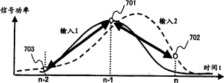
In the DLL circuit, utilize the shift register 601 and 602 that synchronously moves with master clock source 516 that input signal is postponed.In correlator 603, the performance number of n the sampling (Fig. 4 702) of input (n-1) individual sampling of 1 (Fig. 4 701) and input 2 is multiplied each other, and spread all over predetermined interval its result is carried out integration.In correlator 604, the performance number of (n-2) individual sampling (Fig. 4 703) of input (n-1) individual sampling of 1 (Fig. 4 701) and input 2 is multiplied each other, and spread all over predetermined interval its result is carried out integration.Then, obtain the poor of separately integral result, and this difference is transformed into analog signal, be input to VCO513 or 514 by loop filter 607 with DAC606 with adder subtractor 605.
Fig. 4 is the oscillogram of the example that changes the time of the signal power of expression input 1 and input 2.
When asking for the difference of integral result separately with adder subtractor 605,701 the value of then taking a sample is common on both, if 702 and 703 702 the value of relatively taking a sample is bigger, thus the operation result of correlator 603 just become greatly, the output of adder subtractor 605 just become on the occasion of.As shown in Figure 4, the transmission that this means input 1 is regularly regularly compared hysteresis with the transmission of input 2.Therefore, strengthen the output voltage (voltage of VCO control signal) of DLL circuit 511,512, and increase the output frequency of VCO513 and 514.Thus, can make DAC502,503 be taken into the timing advance of input 1 (sending r signal, the θ signal of signal), on direction, control near the timing of importing 2 (the r signal of feedback signal, θ signals).
According to the 1st execution mode, owing to according to the output phase of two VCO the transmission timing of r signal and the transmission of θ signal are regularly controlled independently, so be difficult to mutual stability is brought influence.On the other hand, because the timing of same feedback signal is set as controlled target, so the result just can make both timing unanimity.
In addition, with the method for in the past preset delay amount Comparatively speaking, even taken place because of variations in temperature, also can make the retardation unanimity through the caused variation of its annual change.
Fig. 5 is the block diagram of structure of the RF sending part 403 of expression the present invention the 2nd execution mode.
In the present embodiment, regularly be the timing that benchmark is adjusted feedback signal with the transmission of θ signal, and be the timing that benchmark is adjusted the r signal with the timing of this feedback signal.Basic structure and above-mentioned the 1st execution mode (Fig. 2) beyond the timing adjusting circuit of the RF sending part 403 of present embodiment are common.About part common among the present embodiment, just omit detailed explanation with the 1st execution mode.
In the present embodiment, supply with the clock signal of θ signal, supply with the r signal is used ADC509 with DAC502 and feedback signal clock signal from VCO513, VCO801 respectively with DAC503 from master clock source 516.After feedback signal having been carried out sampling with ADC509 and having made it digitlization, keep with 802 pairs of values of sample-and-hold circuit, so that the r θ split circuit 510 that moves with master clock is not taken into wrong value.
Afterwards, be divided into r (amplitude) composition and θ (phase place) composition with r θ split circuit 510, the r composition compares with the r composition that sends signal in DLL circuit 511 at the r signal, and the θ composition compares with the θ composition of transmission signal in DLL circuit 803 in feedback signal.
DLL circuit 511 and 803, by above-mentioned circuit structure, it is leading (perhaps judge to send in the phase place of the phase place of signal and feedback signal which, lag behind), the output phase of VCO513 and VCO801 is controlled on the direction of above-mentioned judged result convergence (it is consistent with the timing of feedback signal to send signal), wherein, VCO513 supplies with clock signal to the r signal with DAC502, and VCO801 supplies with clock signal to feedback signal with ADC509.In addition, the master clock source 516 that is fixed from output frequency is supplied with the clock of θ signal with DAC503.
In addition, same with the 1st execution mode, under the situation of delay difference more than or equal to 1 clock in the path of the path of r signal and θ signal, its integer part is (in the example of Fig. 5, be equivalent to suppose Δ dr>Δ d θ, and resulting merchant when removing Δ dr-Δ d θ) adjusts with shift-register circuit 515, and control above-mentioned VCO513 and 801 so that the remainder of Δ dr-Δ d θ is adjusted with the clock cycle.Thus, the output signal characteristics that just can improve VCO (for example, C/N), and needn't be widened the control range of the phase place (frequency) of VCO513 and 801.
DLL circuit 511 and 803 structure identical with the 1st execution mode (with reference to Fig. 3).At this, in DLL circuit 511, input 1 is equivalent to send the r composition of signal, and input 2 is equivalent to the r composition of feedback signal, and the output of VCO control signal is connected on the VCO513.In DLL circuit 803, input 1 is equivalent to send the θ composition of signal, and input 2 is equivalent to the θ composition of feedback signal, and the output of VCO control signal is connected on the VCO801.
In addition, though in the present embodiment, following formation promptly, is supplied with the clock of θ signal with DAC503 from master clock source 516, supplies with the clock of r signal with DAC502 from VCO513.But also can followingly constitute, that is, supply with the clock of r signal, supply with the clock of θ signal with DAC503 from VCO513 with DAC502 from master clock source 516.Yet, generally speaking, because the variation of θ composition is littler than the variation of r composition, so adopt structure shown in Figure 5 can access the stability higher than this variation.At this moment, to DLL511 input from the θ signal that sends Signal Separation and go out with from the isolated θ signal of feedback signal, to the DLL803 input from the r signal that sends Signal Separation and go out with from the isolated r signal of feedback signal.
According to present embodiment, by being the timing that benchmark is adjusted feedback signal, to improve the demodulation accuracy of feedback signal with the less θ composition of variation.In addition, owing to supply with master clock to one (being preferably the less θ signal of variation) that send signal, so stability uprises.
Fig. 6 is the block diagram of structure of the RF sending part 403 of expression the present invention the 3rd execution mode.
Present embodiment is to be illustrated in the EER mode transmitter-receiver in addition, under I signal and situation that Q signal is modulated by the path with different retardations, as one of method of the delay difference of adjusting two signal paths, the present invention can also be applicable to the situation of the sender beyond the EER mode.The structure and the 1st execution mode common (with reference to Fig. 1) of part beyond the RF sending part 403 of present embodiment.About part common in the present embodiment, just omit detailed explanation with the 1st execution mode.
The I signal and the Q signal that receive from base band part 402 are transformed into analog signal with DAC901 and 902, be synthesized the line frequency conversion of going forward side by side by filter 903 and 904 I signal and Q signal after quadrature modulator 905 carries out quadrature modulation, be transfused to the signal input terminal of power amplifier 906.The part of the output of power amplifier 906 is distributed to feedback circuit 907 by distributor (coupler etc. omit diagram).In feedback circuit 907, after with frequency translation attenuator circuit 908 power being weakened, become the base band frequency band, and be transformed into digital signal by ADC909 by frequency translation (down-conversion).This feedback signal is carried out quadrature demodulation with IQ split circuit 910 once more, and the I composition compares with the I composition that sends signal in DLL circuit 911 at I signal, and the Q composition compares with the Q composition of transmission signal in DLL circuit 912 at Q signal.
DLL circuit 911 and 912, by above-mentioned circuit structure, judge to send in signal and the feedback signal which in advance (perhaps, lag behind), the output phase of oscillator (VCO) 913 and VCO914 is controlled on the direction of above-mentioned judged result convergence (it is consistent with the timing of feedback signal to send signal), wherein, oscillator (VCO) 913 is supplied with clock signal to I signal with DAC901, and VCO914 supplies with clock signal to Q signal with DAC902.In addition, the oscillator that is fixed from output frequency (master clock source) 516 is supplied with the clock of feedback signal with ADC909.
In addition, the input side in DAC901 and 902 is provided with the sample-and-hold circuit (S/H) that separately input signal is kept.
DLL circuit 911 and 912 structure identical with the 1st execution mode (with reference to Fig. 3).Here, in DLL circuit 911, input 1 is equivalent to send the I composition of signal, and input 2 is equivalent to the I composition of feedback signal, and the output of VCO control signal is connected on the VCO913.In DLL circuit 912, input 1 is equivalent to send the Q composition of signal, and input 2 is equivalent to the Q composition of feedback signal, and the output of VCO control signal is connected on the VCO914.
Generally speaking, the r signal in the delay difference of I composition and Q composition and the EER mode and the delay difference of θ signal are compared little, and be also more according to the unquestioned situation of different wireless communication systems.But, in recent years, along with broadband realization, be able to more utilization with the many-valued modulation headed by the 64QAM (QuardratureAmplitude Modulation), like this, in the IQ modulation system, also need further to improve linear property, the importance increase of present embodiment even can think.
Utilize possibility on the industry
The present invention can be used in the base station of the wireless communication system headed by the portable phone or end The transmitter receiver of end helps the waveform quality (linear) of output signal to improve. Because Along with signal quality improves, just can adopt efficient higher EER mode or saturability higher Power amplifier is so help the reduction of power consumption.

Claims (12)

1. transtation mission circuit is characterized in that having:
The digital-to-analog translation circuit will be transformed into analog signal respectively from two signals or separated back two digital signals importing that the digital signal of being imported is separated;
Combiner circuit is to being synthesized by the above-mentioned analog signal of above-mentioned digital-to-analog translation circuit institute conversion;
Distributor circuit, a part of taking out the above-mentioned signal that synthesizes is as feedback signal;
Analog/digital conversion circuit is transformed into digital signal with above-mentioned feedback signal;
Oscillating circuit is supplied with the Action clock signal to above-mentioned each digital-to-analog translation circuit and above-mentioned analog/digital conversion circuit;
First split circuit will be separated into two signals by the feedback signal of above-mentioned analog/digital conversion circuit institute conversion; And
Comparison circuit, at least one at least one that will be from two signals that the digital signal imported is separated or two digital signals of separated back input compares with the feedback signal of being separated by above-mentioned first split circuit,
Wherein, above-mentioned oscillating circuit is controlled its output according to the comparative result by means of comparison circuit.
2. according to the described transtation mission circuit of claim 1, it is characterized in that:
Also have second split circuit, the digital signal that is imported into above-mentioned transtation mission circuit is separated into two signals;
Wherein, above-mentioned digital-to-analog translation circuit is made of first digital-to-analog converter and second digital-to-analog converter;
Above-mentioned comparison circuit relatively by above-mentioned second split circuit input signal that is separated and the feedback signal of being separated by above-mentioned first split circuit, is judged the timing difference of two signals;
Above-mentioned oscillating circuit is supplied with clock signal to above-mentioned first digital-to-analog converter, above-mentioned second digital-to-analog converter, above-mentioned analog/digital conversion circuit, to be fed into some clock signals is that benchmark is controlled being fed into other clock signals of two, so that above-mentioned timing difference diminishes.
3. according to the described transtation mission circuit of claim 2, it is characterized in that:
Above-mentioned second split circuit separates the amplitude composition and the phase component of the above-mentioned digital signal of importing;
Above-mentioned first digital-to-analog converter is transformed into analog signal with above-mentioned amplitude composition;
Above-mentioned second digital-to-analog converter is transformed into analog signal with above-mentioned phase component;
Above-mentioned combiner circuit is made of amplifying circuit, the synthetic phase component that is transformed into the amplitude composition of above-mentioned analog signal and is transformed into above-mentioned analog signal of this amplifying circuit;
Above-mentioned first split circuit separates the amplitude composition and the phase component of above-mentioned feedback signal;
Above-mentioned comparison circuit, constitute by first comparator and second comparator, wherein, this first comparator, compare the amplitude composition of the input signal that is separated by above-mentioned second split circuit and the amplitude composition of the feedback signal of being separated, judge the timing difference of two signals by above-mentioned first split circuit; This second comparator relatively by the phase component of above-mentioned second split circuit phase of input signals composition that is separated and the feedback signal of being separated by above-mentioned first split circuit, is judged the timing difference of two signals;
Above-mentioned oscillating circuit is by reference oscillator from clock signal to above-mentioned analog/digital conversion circuit that supply with; Supply with first variable oscillator of clock signal to above-mentioned first digital-to-analog converter; And second variable oscillator formation from clock signal to above-mentioned second digital-to-analog converter that supply with;
The output of above-mentioned first variable oscillator is controlled according to the comparative result of above-mentioned first comparator, the output of above-mentioned second variable oscillator is controlled according to the comparative result of above-mentioned second comparator, makes the timing coupling of the amplitude composition that is transfused to above-mentioned amplifying circuit and phase component thus.
4. according to the described transtation mission circuit of claim 2, it is characterized in that:
Above-mentioned second split circuit separates the amplitude composition and the phase component of the above-mentioned digital signal of importing;
Above-mentioned first digital-to-analog converter is transformed into analog signal with above-mentioned amplitude composition;
Above-mentioned second digital-to-analog converter is transformed into analog signal with above-mentioned phase component;
Above-mentioned combiner circuit is made of amplifying circuit, the synthetic phase component that is transformed into the amplitude composition of above-mentioned analog signal and is transformed into above-mentioned analog signal of this amplifying circuit;
Above-mentioned first split circuit separates the amplitude composition and the phase component of above-mentioned feedback signal;
Above-mentioned comparison circuit, constitute by first comparator and second comparator, wherein, this first comparator, compare the amplitude composition of the input signal that is separated by above-mentioned second split circuit and the amplitude composition of the feedback signal of being separated, judge the timing difference of two signals by above-mentioned first split circuit; This second comparator relatively by the phase component of above-mentioned second split circuit phase of input signals composition that is separated and the feedback signal of being separated by above-mentioned first split circuit, is judged the timing difference of two signals;
Above-mentioned oscillating circuit is by second variable oscillator from clock signal to above-mentioned analog/digital conversion circuit that supply with; Supply with first variable oscillator of clock signal to above-mentioned first digital-to-analog converter; And reference oscillator formation from clock signal to above-mentioned second digital-to-analog converter that supply with;
The output of above-mentioned first variable oscillator is controlled according to the comparative result of above-mentioned first comparator, the output of above-mentioned second variable oscillator is controlled according to the comparative result of above-mentioned second comparator, makes the timing coupling of the amplitude composition that is transfused to above-mentioned amplifying circuit and phase component thus.
5. according to the described transtation mission circuit of claim 1, it is characterized in that:
Above-mentioned digital-to-analog translation circuit, constitute by first digital-to-analog converter and second digital-to-analog converter, wherein, this first digital-to-analog converter is transformed into analog signal with the orthogonal component of the digital signal imported, and this second digital-to-analog converter is transformed into analog signal with the same phase constituent of the digital signal imported;
Above-mentioned combiner circuit is made of modulation circuit, and the orthogonal component that this modulation circuit utilization is transformed into above-mentioned analog signal carries out quadrature modulation with the same phase constituent that is transformed into above-mentioned analog signal;
Above-mentioned first split circuit separates the orthogonal component and the same phase constituent of above-mentioned feedback signal;
Above-mentioned comparison circuit is made of first comparator and second comparator, and wherein, this first comparator relatively by the orthogonal component of the feedback signal of above-mentioned analog/digital conversion circuit institute conversion and the orthogonal component of above-mentioned input signal, is judged the timing difference of each signal; This second comparator relatively by the same phase constituent of the feedback signal of above-mentioned analog/digital conversion circuit institute conversion and the same phase constituent of above-mentioned input signal, is judged the timing difference of each signal;
Above-mentioned oscillating circuit is by reference oscillator from clock signal to above-mentioned analog/digital conversion circuit that supply with; Supply with first variable oscillator of clock signal to above-mentioned first digital-to-analog converter; And second variable oscillator formation from clock signal to above-mentioned second digital-to-analog converter that supply with;
The output of above-mentioned first variable oscillator is controlled according to the comparative result of above-mentioned first comparator, the output of above-mentioned second variable oscillator is controlled according to the comparative result of above-mentioned second comparator, and the orthogonal component that is transfused to above-mentioned modulation circuit is mated with the timing with phase constituent.
6. according to the described transtation mission circuit of claim 1, it is characterized in that:
Also have data holding circuit, keep having supplied with the above-mentioned digital-to-analog translation circuit of clock signal and/or the digital signal of above-mentioned analog/digital conversion circuit input and output from above-mentioned first variable oscillator or second variable oscillator.
7. a radio communication device is characterized in that: possess the described transtation mission circuit of claim 1.
8. the timing adjusting method of a transtation mission circuit is characterized in that, comprising:
The 1st step will be transformed into analog signal respectively from two signals or separated back two digital signals importing that the digital signal of being imported is separated;
The 2nd step is synthesized the above-mentioned analog signal of institute's conversion in above-mentioned the 1st step;
The 3rd step, a part of taking out the signal that is synthesized in above-mentioned the 2nd step is as feedback signal;
The 4th step, the feedback signal that will be taken out in above-mentioned the 3rd step is transformed into digital signal;
The 5th step, the feedback signal that will be transformed into digital signal in above-mentioned the 4th step is separated into two signals;
The 6th step, at least one at least one that will be from two signals that the digital signal imported is separated or two digital signals of separated back input compares with the feedback signal of being separated in above-mentioned the 5th step; And
The 7th step according to the comparative result in above-mentioned the 6th step, is controlled the clock signal of the analog-to-digital conversion of the digitaltoanalogconversion of above-mentioned the 1st step and/or above-mentioned the 4th step.
9. according to the timing adjusting method of the described transtation mission circuit of claim 8, it is characterized in that:
Also comprise the 8th step, the digital signal that is used for being imported into above-mentioned transtation mission circuit is separated into two signals;
Wherein, above-mentioned the 6th step compares input signal that is separated and the feedback signal of being separated in above-mentioned the 5th step in above-mentioned the 8th step, judge the timing difference of two signals;
Above-mentioned the 7th step according to the comparative result in above-mentioned the 6th step, is controlled the clock signal of the analog-to-digital conversion of the digitaltoanalogconversion of above-mentioned the 1st step and/or above-mentioned the 4th step, so that above-mentioned timing difference diminishes.
10. according to the timing adjusting method of the described transtation mission circuit of claim 9, it is characterized in that:
Above-mentioned the 8th step is separated the amplitude composition and the phase component of the above-mentioned digital signal of importing;
Above-mentioned the 1st step is transformed into analog signal with above-mentioned amplitude composition, and, above-mentioned phase component is transformed into analog signal;
Above-mentioned the 2nd step is with the synthetic phase component that is transformed into the amplitude composition of above-mentioned analog signal and is transformed into above-mentioned analog signal of amplifying circuit;
Above-mentioned the 5th step is separated the amplitude composition and the phase component of above-mentioned feedback signal;
Above-mentioned the 6th step, compare the amplitude composition of the input signal that in above-mentioned the 8th step, is separated and the amplitude composition of the feedback signal of in above-mentioned the 5th step, being separated, judge the timing difference of two signals, and, the phase component of phase of input signals composition that is separated in above-mentioned the 8th step and the feedback signal of being separated in above-mentioned the 5th step is relatively judged the timing difference of two signals;
Above-mentioned the 7th step, comparative result according to the amplitude composition of above-mentioned the 6th step, be controlled at clock signal used when the above-mentioned amplitude composition in above-mentioned the 2nd step is transformed into analog signal, and according to the comparative result of the phase component of above-mentioned the 6th step, be controlled at clock signal used when the above-mentioned phase component in above-mentioned the 2nd step is transformed into analog signal, make the amplitude composition that is imported into above-mentioned amplifying circuit and the timing coupling of phase component thus.
11. the timing adjusting method according to the described transtation mission circuit of claim 9 is characterized in that:
Above-mentioned the 8th step is separated the amplitude composition and the phase component of the above-mentioned digital signal of importing;
Above-mentioned the 1st step is transformed into analog signal with above-mentioned amplitude composition, and, above-mentioned phase component is transformed into analog signal;
Above-mentioned the 2nd step is with the synthetic phase component that is transformed into the amplitude composition of above-mentioned analog signal and is transformed into above-mentioned analog signal of amplifying circuit;
Above-mentioned the 5th step is separated the amplitude composition and the phase component of above-mentioned feedback signal;
Above-mentioned the 6th step, compare the amplitude composition of the input signal that in above-mentioned the 8th step, is separated and the amplitude composition of the feedback signal of in above-mentioned the 5th step, being separated, judge the timing difference of two signals, and, the phase component of phase of input signals composition that is separated in above-mentioned the 8th step and the feedback signal of being separated in above-mentioned the 5th step is relatively judged the timing difference of two signals;
Above-mentioned the 7th step, comparative result according to the amplitude composition of above-mentioned the 6th step, be controlled at clock signal used when the above-mentioned amplitude composition in above-mentioned the 2nd step is transformed into analog signal, and according to the comparative result of the phase component of above-mentioned the 6th step, be controlled at feedback signal with above-mentioned the 4th step used clock signal when being transformed into digital signal, make the amplitude composition that is imported into above-mentioned amplifying circuit and the timing coupling of phase component thus.
12. the timing adjusting method according to the described transtation mission circuit of claim 8 is characterized in that:
Above-mentioned the 1st step is transformed into analog signal with the orthogonal component of the digital signal imported, and, the same phase constituent of the digital signal imported is transformed into analog signal;
Above-mentioned the 2nd step is with the synthetic same phase constituent that is transformed into the orthogonal component of above-mentioned analog signal and is transformed into above-mentioned analog signal of quadrature modulation circuit;
Above-mentioned the 5th step is separated the orthogonal component and the same phase constituent of above-mentioned feedback signal;
Above-mentioned the 6th step, the relatively orthogonal component of the feedback signal of institute's conversion and the orthogonal component of above-mentioned input signal in above-mentioned the 4th step, judge the timing difference of each signal, and, the relatively same phase constituent of the feedback signal of institute's conversion and the same phase constituent of above-mentioned input signal in above-mentioned the 4th step are judged the timing difference of each signal;
Above-mentioned the 7th step, comparative result according to the orthogonal component of above-mentioned the 6th step, be controlled at clock signal used when the above-mentioned orthogonal component in above-mentioned the 2nd step is transformed into analog signal, and according to the comparative result of the same phase constituent of above-mentioned the 6th step, be controlled at clock signal used when above-mentioned in above-mentioned the 2nd step be transformed into analog signal with phase constituent, make the orthogonal component that is imported into above-mentioned modulation circuit and timing coupling thus with phase constituent.
CNB200410081805XA 2004-01-14 2004-12-30 The timing adjusting method of transtation mission circuit, radio communication device and transtation mission circuit Expired - Fee Related CN100542055C (en)

Applications Claiming Priority (2)

Application Number Priority Date Filing Date Title
JP2004006864A JP4323968B2 (en) 2004-01-14 2004-01-14 Timing adjustment method for wireless communication device
JP2004006864 2004-01-14

Publications (2)

Publication Number Publication Date
CN1642025A CN1642025A (en) 2005-07-20
CN100542055C true CN100542055C (en) 2009-09-16

Family

ID=34697847

Family Applications (1)

Application Number Title Priority Date Filing Date
CNB200410081805XA Expired - Fee Related CN100542055C (en) 2004-01-14 2004-12-30 The timing adjusting method of transtation mission circuit, radio communication device and transtation mission circuit

Country Status (5)

Country Link
US (2) US7383028B2 (en)
EP (1) EP1564910A3 (en)
JP (1) JP4323968B2 (en)
KR (1) KR101121694B1 (en)
CN (1) CN100542055C (en)

Families Citing this family (35)

* Cited by examiner, † Cited by third party
Publication number Priority date Publication date Assignee Title
JP4323968B2 (en) * 2004-01-14 2009-09-02 株式会社日立コミュニケーションテクノロジー Timing adjustment method for wireless communication device
US7983632B2 (en) * 2004-09-24 2011-07-19 Broadcom Corporation Feedback control loop for amplitude modulation in a polar transmitter with a translational loop
WO2006054464A1 (en) * 2004-11-17 2006-05-26 Matsushita Electric Industrial Co., Ltd. Transmitting circuit, transmitting method, and communication device using the same
WO2006066628A1 (en) * 2004-12-23 2006-06-29 Freescale Semiconductor, Inc Power control system for a wireless communication unit
DE602004032064D1 (en) * 2004-12-23 2011-05-12 Freescale Semiconductor Inc WIRELESS COMMUNICATION UNIT AND PERFORMANCE CONTROL SYSTEM FOR THIS
FI20055355A0 (en) * 2005-06-29 2005-06-29 Nokia Corp Method for data processing, pre-distortion arrangement, transmitter, network element and base station
FI20055354A0 (en) * 2005-06-29 2005-06-29 Nokia Corp Data processing method, transmitter, device, network element and base station
KR100646855B1 (en) * 2005-10-07 2006-11-23 한국전자통신연구원 Apparatus and method of nonlinear distortion correction using characteristics modeling of high power amplifier
JP4652974B2 (en) * 2005-12-27 2011-03-16 富士通株式会社 Timing adjustment apparatus and timing adjustment method
JP4951238B2 (en) * 2005-12-27 2012-06-13 パナソニック株式会社 Polar coordinate modulation transmission apparatus, adaptive distortion compensation processing system, polar modulation transmission method, and adaptive distortion compensation processing method
WO2007074839A1 (en) * 2005-12-27 2007-07-05 Matsushita Electric Industrial Co., Ltd. Multimode-corresponding polar-coordinate modulating transmission device, and multimode radio communication method
JP2007189438A (en) * 2006-01-12 2007-07-26 Fujitsu Ltd Timing adjusting device and timing adjusting method
US20070264026A1 (en) * 2006-05-10 2007-11-15 Miguel Joseph D Method and apparatus for controlling phase of a clock signal
KR100847801B1 (en) * 2007-02-21 2008-07-23 지씨티 세미컨덕터 인코포레이티드 Apparatus and method for measuring iq mismatch
FR2920265A1 (en) * 2007-08-23 2009-02-27 Eads Secure Networks Soc Par A CORRECTION OF DISTORTIONS IN A TRANSMISSION CHAIN
KR101201911B1 (en) * 2007-10-10 2012-11-20 삼성전자주식회사 Apparatus and method for power amplifier with delay control in wireless communication system
US8283786B2 (en) 2007-12-21 2012-10-09 Advanced Micro Devices, Inc. Integrated circuit system with contact integration
US8023909B2 (en) * 2009-01-12 2011-09-20 Skyworks Solutions, Inc. Data conversion using a serial interface clock in a power amplifier module
US8044742B2 (en) 2009-03-11 2011-10-25 Qualcomm Incorporated Wideband phase modulator
US8588720B2 (en) 2009-12-15 2013-11-19 Qualcomm Incorproated Signal decimation techniques
JP2011135347A (en) 2009-12-24 2011-07-07 Panasonic Corp Transmission circuit, and communication apparatus
CN102812746B (en) * 2010-03-31 2015-04-08 松下电器(美国)知识产权公司 Wireless communication device and wireless communication method
CN102377432B (en) * 2010-08-27 2015-01-07 国民技术股份有限公司 Multiplex analog-to-digital conversion device
CN103095304B (en) * 2011-11-07 2016-03-16 国民技术股份有限公司 One is orthogonal signal analog-digital converter in the same way
CN103312274B (en) * 2012-03-16 2016-03-16 京信通信系统(中国)有限公司 A kind of digital control method of feed-forward amplifier and digitlization feed-forward amplifier
WO2013158101A1 (en) 2012-04-19 2013-10-24 Intel Corporation A signal amplifier with active power management
US9000858B2 (en) 2012-04-25 2015-04-07 Qualcomm Incorporated Ultra-wide band frequency modulator
JP5743221B2 (en) * 2012-06-29 2015-07-01 カシオ計算機株式会社 Wireless synchronization system, wireless device, sensor device, wireless synchronization method, and program
US8909180B1 (en) * 2013-06-26 2014-12-09 Motorola Solutions, Inc. Method and apparatus for power supply modulation of a radio frequency signal
JP6320794B2 (en) 2014-02-28 2018-05-09 株式会社東芝 Signal processing device
US9325491B2 (en) * 2014-04-15 2016-04-26 Triquint Semiconductor, Inc. Clock generation circuit with dual phase-locked loops
CN111512588A (en) * 2017-10-24 2020-08-07 天波网络有限责任公司 Clock synchronization when switching between broadcast and data transfer modes
EP3570602B1 (en) * 2018-05-15 2021-03-24 Nxp B.V. Apparatus and methods for synchronization of transmitters
CN109348493B (en) * 2018-10-24 2022-02-11 广州天电科技有限公司 High-reliability wireless communication system link backup device and control method thereof
KR102623191B1 (en) * 2022-03-04 2024-01-11 주식회사 램쉽 Echo canceller for asymmetric full-duplex transceiver

Citations (2)

* Cited by examiner, † Cited by third party
Publication number Priority date Publication date Assignee Title
CN1267137A (en) * 1999-01-28 2000-09-20 日本电气株式会社 Sending timing adjusting circuit and method
JP2001189685A (en) * 1999-12-28 2001-07-10 Fujitsu Ltd Distortion compensator

Family Cites Families (36)

* Cited by examiner, † Cited by third party
Publication number Priority date Publication date Assignee Title
WO1984001949A1 (en) * 1982-11-10 1984-05-24 Kyoto Pharma Ind Cephalosporin derivatives, process and their preparation, and prophylactic and treating agent against bacterial infection
US5175879A (en) 1991-04-25 1992-12-29 Motorola, Inc. Linear amplifier with feedback path and phase error compensation
IT1265271B1 (en) * 1993-12-14 1996-10-31 Alcatel Italia BASEBAND PREDISTRITORTION SYSTEM FOR THE ADAPTIVE LINEARIZATION OF POWER AMPLIFIERS
JP2967699B2 (en) * 1995-03-06 1999-10-25 日本電気株式会社 Transmission device
US5543896A (en) * 1995-09-13 1996-08-06 Xerox Corporation Method for measurement of tone reproduction curve using a single structured patch
WO1997049174A1 (en) * 1996-06-19 1997-12-24 Fraunhofer-Gesellschaft zur Förderung der angewandten Forschung e.V. Pre-distortion for a non-linear transmission path in the high frequency range
US5903797A (en) * 1997-08-15 1999-05-11 Xerox Corporation Monitoring cleaning performance to predict cleaner life
US5887221A (en) * 1997-10-20 1999-03-23 Xerox Corporation Signature sensing for optimum toner control with donor roll
US6137826A (en) * 1997-11-17 2000-10-24 Ericsson Inc. Dual-mode modulation systems and methods including oversampling of narrow bandwidth signals
JP2000124963A (en) * 1998-10-19 2000-04-28 Alps Electric Co Ltd Base band signal processing circuit
GB9825414D0 (en) 1998-11-19 1999-01-13 Symbionics Limted Linear RF power amplifier and transmitter
US6275685B1 (en) * 1998-12-10 2001-08-14 Nortel Networks Limited Linear amplifier arrangement
JP4256057B2 (en) * 1999-09-30 2009-04-22 株式会社東芝 Nonlinear compensator
DE69932723T2 (en) * 1999-09-30 2007-09-06 Kabushiki Kaisha Toshiba, Kawasaki Non-linear correction device
US6272295B1 (en) * 1999-11-24 2001-08-07 Xerox Corporation Apparatus including and use of an enhanced toner area coverage sensor to monitor filming levels on a photoreceptor surface
JP2001313532A (en) * 2000-05-01 2001-11-09 Sony Corp Distortion compensation device
JP2002084146A (en) 2000-09-08 2002-03-22 Hitachi Ltd Predistortion type distortion compensated power amplifier
CN1252910C (en) * 2000-10-17 2006-04-19 艾利森电话股份有限公司 Communications systems
US6801784B1 (en) * 2000-11-02 2004-10-05 Skyworks Solutions, Inc. Continuous closed-loop power control system including modulation injection in a wireless transceiver power amplifier
SE519258C2 (en) * 2000-11-24 2003-02-04 Ericsson Telefon Ab L M Transmitter
SE520530C2 (en) * 2001-04-26 2003-07-22 Ericsson Telefon Ab L M Linearized switch-based power amplifier
JP2002368708A (en) 2001-06-08 2002-12-20 Hitachi Ltd Multi-carrier digital pre-distortion device
JP4012725B2 (en) 2001-12-05 2007-11-21 株式会社日立コミュニケーションテクノロジー Predistortion type amplifier
FR2835120B1 (en) 2002-01-21 2006-10-20 Evolium Sas METHOD AND DEVICE FOR PREPARING SIGNALS TO BE COMPARED TO ESTABLISH PRE-DISTORTION ON THE INPUT OF AN AMPLIFIER
US7085330B1 (en) * 2002-02-15 2006-08-01 Marvell International Ltd. Method and apparatus for amplifier linearization using adaptive predistortion
JP2003273663A (en) 2002-03-15 2003-09-26 Hitachi Ltd Predistortion type amplifier
FR2837647B1 (en) * 2002-03-25 2006-11-24 Canon Kk WIRELESS TRANSMITTER WITH REDUCED POWER CONSUMPTION
JP4071526B2 (en) * 2002-04-10 2008-04-02 松下電器産業株式会社 Nonlinear distortion compensation apparatus and transmission apparatus
US7346125B2 (en) * 2002-04-23 2008-03-18 Raytheon Company Method and device for pulse shaping QPSK signals
JP3923978B2 (en) * 2002-05-31 2007-06-06 富士通株式会社 Adaptive controller
KR100448892B1 (en) * 2002-06-04 2004-09-18 한국전자통신연구원 Apparatus and Method for Pre-distortion for Nonlinear Distortion of High Power Amplifier
US7184491B2 (en) 2002-09-05 2007-02-27 Htachi, Ltd. Wireless communication apparatus
US7263135B2 (en) * 2002-10-03 2007-08-28 Matsushita Electric Industrial Co., Ltd. Transmitting method and transmitter apparatus
JP4230238B2 (en) * 2003-02-06 2009-02-25 パナソニック株式会社 Transmitting apparatus and adjustment method thereof
US7349490B2 (en) * 2003-04-16 2008-03-25 Powerwave Technologies, Inc. Additive digital predistortion system employing parallel path coordinate conversion
JP4323968B2 (en) * 2004-01-14 2009-09-02 株式会社日立コミュニケーションテクノロジー Timing adjustment method for wireless communication device

Patent Citations (2)

* Cited by examiner, † Cited by third party
Publication number Priority date Publication date Assignee Title
CN1267137A (en) * 1999-01-28 2000-09-20 日本电气株式会社 Sending timing adjusting circuit and method
JP2001189685A (en) * 1999-12-28 2001-07-10 Fujitsu Ltd Distortion compensator

Also Published As

Publication number Publication date
KR20050074917A (en) 2005-07-19
EP1564910A3 (en) 2010-05-26
EP1564910A2 (en) 2005-08-17
CN1642025A (en) 2005-07-20
JP2005203960A (en) 2005-07-28
JP4323968B2 (en) 2009-09-02
KR101121694B1 (en) 2012-03-22
US20050153669A1 (en) 2005-07-14
US7383028B2 (en) 2008-06-03
US20080233904A1 (en) 2008-09-25
US7933569B2 (en) 2011-04-26

Similar Documents

Publication Publication Date Title
CN100542055C (en) The timing adjusting method of transtation mission circuit, radio communication device and transtation mission circuit
US7783263B2 (en) Simplified digital predistortion in a time-domain duplexed transceiver
EP1155499B1 (en) Method and apparatus for linear amplification of a radio frequency signal
US6266517B1 (en) Method and apparatus for correcting distortion in a transmitter
US8224266B2 (en) Power amplifier predistortion methods and apparatus using envelope and phase detector
US6647073B2 (en) Linearisation and modulation device
CN100481741C (en) Amplifier circuit, wireless base station, wireless terminal, and amplifying method
US20080111622A1 (en) Hybrid Doherty Amplifier System and Method
US20020048326A1 (en) Method and apparatus for plurality signal generation
US20030156658A1 (en) Method and apparatus for preparing signals to be compared to establish predistortion at the input of an amplifier
WO2004032345A1 (en) Transmitting method and transmitter apparatus
WO2005093962A1 (en) Radio system, radio transmitter, and radio receiver
JPH08163189A (en) Transmission circuit
KR20020008456A (en) Base station transmit unit with feed-forward mode linearization unit
KR20040080353A (en) Signal sample acquisition techniques
KR101102109B1 (en) Feedforward linearization of rf power amplifiers
US8532590B2 (en) Digital phase feedback for determining phase distortion
US6904267B2 (en) Amplifying device
JP2007019703A (en) Transmitting/receiving device
WO2004034574A1 (en) Distortion compensation amplification apparatus, amplification system, and radio base station
WO2015114702A1 (en) Transmission device and method for controlling same
JP2002151973A (en) Transmitter and pre-distortion compensation method
JP6286908B2 (en) Amplifying device and wireless communication device
WO2005048462A3 (en) System and method for an improved quadrature upconverter for i/q modulation using intermediate frequency carriers
Nair et al. Effect of Time Synchronisation in Digital Predistorter Enabled SWIPT Networks

Legal Events

Date Code Title Description
C06 Publication
PB01 Publication
C10 Entry into substantive examination
SE01 Entry into force of request for substantive examination
C14 Grant of patent or utility model
GR01 Patent grant
ASS Succession or assignment of patent right

Owner name: HITACHI CO., LTD.

Free format text: FORMER OWNER: HITACHI COMMUNICATION TECHNOLOGIES LTD.

Effective date: 20100318

C41 Transfer of patent application or patent right or utility model
TR01 Transfer of patent right

Effective date of registration: 20100318

Address after: Tokyo, Japan

Patentee after: Hitachi Ltd.

Address before: Tokyo, Japan

Patentee before: Hitachi Communications Technology Co., Ltd.

CF01 Termination of patent right due to non-payment of annual fee

Granted publication date: 20090916

Termination date: 20141230

EXPY Termination of patent right or utility model