JP3923978B2 - Adaptive controller - Google Patents
Adaptive controller Download PDFInfo
- Publication number
- JP3923978B2 JP3923978B2 JP2004510127A JP2004510127A JP3923978B2 JP 3923978 B2 JP3923978 B2 JP 3923978B2 JP 2004510127 A JP2004510127 A JP 2004510127A JP 2004510127 A JP2004510127 A JP 2004510127A JP 3923978 B2 JP3923978 B2 JP 3923978B2
- Authority
- JP
- Japan
- Prior art keywords
- delay time
- unit
- signal
- delay
- adaptive control
- Prior art date
- Legal status (The legal status is an assumption and is not a legal conclusion. Google has not performed a legal analysis and makes no representation as to the accuracy of the status listed.)
- Expired - Fee Related
Links
Images


Classifications
-
- H—ELECTRICITY
- H03—ELECTRONIC CIRCUITRY
- H03F—AMPLIFIERS
- H03F1/00—Details of amplifiers with only discharge tubes, only semiconductor devices or only unspecified devices as amplifying elements
- H03F1/32—Modifications of amplifiers to reduce non-linear distortion
-
- H—ELECTRICITY
- H03—ELECTRONIC CIRCUITRY
- H03F—AMPLIFIERS
- H03F1/00—Details of amplifiers with only discharge tubes, only semiconductor devices or only unspecified devices as amplifying elements
- H03F1/02—Modifications of amplifiers to raise the efficiency, e.g. gliding Class A stages, use of an auxiliary oscillation
-
- H—ELECTRICITY
- H03—ELECTRONIC CIRCUITRY
- H03F—AMPLIFIERS
- H03F1/00—Details of amplifiers with only discharge tubes, only semiconductor devices or only unspecified devices as amplifying elements
- H03F1/32—Modifications of amplifiers to reduce non-linear distortion
- H03F1/3241—Modifications of amplifiers to reduce non-linear distortion using predistortion circuits
- H03F1/3247—Modifications of amplifiers to reduce non-linear distortion using predistortion circuits using feedback acting on predistortion circuits
-
- H—ELECTRICITY
- H03—ELECTRONIC CIRCUITRY
- H03F—AMPLIFIERS
- H03F1/00—Details of amplifiers with only discharge tubes, only semiconductor devices or only unspecified devices as amplifying elements
- H03F1/34—Negative-feedback-circuit arrangements with or without positive feedback
- H03F1/345—Negative-feedback-circuit arrangements with or without positive feedback using hybrid or directional couplers
-
- H—ELECTRICITY
- H03—ELECTRONIC CIRCUITRY
- H03F—AMPLIFIERS
- H03F3/00—Amplifiers with only discharge tubes or only semiconductor devices as amplifying elements
- H03F3/20—Power amplifiers, e.g. Class B amplifiers, Class C amplifiers
- H03F3/24—Power amplifiers, e.g. Class B amplifiers, Class C amplifiers of transmitter output stages
-
- H—ELECTRICITY
- H04—ELECTRIC COMMUNICATION TECHNIQUE
- H04B—TRANSMISSION
- H04B1/00—Details of transmission systems, not covered by a single one of groups H04B3/00 - H04B13/00; Details of transmission systems not characterised by the medium used for transmission
- H04B1/02—Transmitters
- H04B1/04—Circuits
- H04B2001/0408—Circuits with power amplifiers
- H04B2001/045—Circuits with power amplifiers with means for improving efficiency
Description
本発明は適応制御装置に係わり、特に、参照信号とフィードバック信号間の遅延時間が零となるように遅延時間を調整する機能を備えた適応制御装置に関する。 The present invention relates to an adaptive control device, and more particularly to an adaptive control device having a function of adjusting a delay time so that a delay time between a reference signal and a feedback signal becomes zero.
一般にフィードバック信号を使用して適応制御する装置では、参照信号とフィードバック信号の差を演算し、該差が小さくなるように適応制御し、参照信号に適応制御結果を反映して出力する。
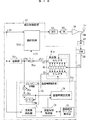
図19は電力増幅器で発生する歪を補償するための適応制御装置1の構成図であり、参照信号である送信信号x(t)とフィードバック信号y(t)の差を演算する誤差演算部1a、参照信号とフィードバック信号間の遅延時間が零となるように各信号を遅延させる遅延部1b,1c、該差e(t)が小さくなるように適応制御すると共に参照信号に適応制御結果を反映させる適応制御部1dを備えている。適応制御部1dは、参照信号に適応制御結果を反映することにより得られた信号を変調部2に入力し、変調部2は入力信号に変調処理を施し、DA変換器3は変調信号をアナログ信号に変換して電力増幅器4に入力し、電力増幅器4は入力信号を増幅してアンテナ5より空間に放射する。方向結合器6は電力増幅器出力の一部分を取り出してAD変換器7を介して復調部8に入力し、復調部8は入力信号に復調処理を施して適応制御装置1に入力する。誤差演算部1aは遅延部1b,1cを介して入力する参照信号x′(t)とフィードバック信号y′(t)の差e(t)を演算し、適応制御部1dは該差e(t)が小さくなるように適応制御し、次の参照信号に適応制御結果を反映する。以上の制御により、フィードバック信号を歪のない参照信号と一致させることができる。すなわち、電力増幅器4で発生する歪を補償でき、歪のない信号を送信することができる。
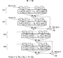
図20は適応制御部の動作説明図であり、参照信号x(t)に適応制御結果を反映して出力する反映部11と適応制御演算部12を有している。反映部11において、乗算器(プリディストーション部)11aは送信信号x(t)に歪補償係数hn(p)を乗算して乗算結果を出力する。歪補償係数記憶部11bは送信信号x(t)のパワーp(=|x(t)|2)に応じた歪補償係数hn(p)を記憶するもので、適応制御演算部12のLMS適応アルゴリズムで求まる歪補償係数hn+1(p)により歪補償係数hn(p)を更新する。アドレス発生部11cは送信信号x(t)のパワーp(=|x(t)|2)を演算し、読み出しアドレスARとして出力する。遅延部11dは歪補償係数記憶部11bの書き込みアドレスAWを発生する。送信信号x(t)のパワーpが示すアドレスARから歪補償係数hn(p)が読出され、新たな歪補償係数hn+1(p)が求まるまでに所定の時間を要する。そこで、遅延部11dは書き込みアドレスの発生をこの時間分遅延させ、新たな歪補償係数hn+1(p)で古い歪補償係数hn(p)を更新できるようにする。
適応制御演算部12において、乗算器12aは送信信号x′(t)とフィードバック信号y′(t)との差信号e(t)とステップサイズパラメータμ(<1)を乗算し、共役複素信号出力部12bは共役複素信号y*(t)を出力する。乗算器12cは、歪補償係数hn(p)とy*(t)の乗算を行い、乗算器12dはμe(t)とu*(t)の乗算を行う。遅延部12eは歪補償係数hn(p)を出力するタイミングを調整し、加算器12fは歪補償係数hn(p)とμe(t)u*(t)を加算し、新たな歪補償係数hn+1(p)を出力する。
上記構成により、以下に示す演算が行われる。但し、電力増幅器4は歪関数f(p)を有しているものとする。
hn+1(p)=hn(p)+μe(t)u*(t)
e(t)=x(t)−y(t)
y(t)=hn(p)x(t)f(p)
u(t)=x(t)f(p)=hn *(p)y(t)
P=|x(t)|2
hn *(p) hn(p)=1
x,y,f,h,u,eは複素数、*は共役複素数である。
上記演算処理を行うことにより歪補償係数hn(p)が更新され、最終的に最適の歪補償係数値に収束し、電力増幅器4の歪が補償される。
以上より、参照信号x(t)が適応制御装置1に入力して誤差演算部1aに到達するまでの遅延時間と、フィードバック信号y(t)が誤差演算部1aに到達するまでの遅延時間を等しくする必要がある。このため、従来は、図21に示すように遅延時間制御部9を設けて遅延部1cの遅延時間を制御して参照信号とフィードバック信号の誤差演算部1aに入力するタイミングを一致させている。すなわち、遅延時間制御部9はフィードバック信号の遅延時間を変えながら、相関器9aにおいて遅延部1bから出力する参照信号と遅延部1cから出力するフィードバック信号の相関を演算し、遅延時間設定部9bにおいて相関が最大となる遅延時間を求め、該遅延時間を遅延部1cに設定する。これにより、参照信号x(t)が適応制御装置1に入力して誤差演算部1aに到達するまでの遅延時間と、フィードバック信号y(t)が誤差演算部1aに到達するまでの遅延時間を等しくできる。
ところで、フィードバック信号の遅延時間は、参照信号の周波数帯域、帯域幅などにより変化する。このため、参照信号の周波数成分が一定であれば問題ないが、周波数成分が変化すると、参照信号x(t)が誤差演算部1aに到達するまでの遅延時間と、フィードバック信号y(t)が誤差演算部1aに到達するまでの遅延時間が等しくなくなり、適応制御を良好に行えなくなる。例えば、適応制御により電力増幅器の歪補償をする場合、歪補償係数が最適な収束をせずノイズフロアが上昇する。なお、遅延時間制御部9がリアルタイムに遅延時間制御する場合であっても、遅延時間制御が周波数変化に追従して高速に制御することができず、上記問題が発生する。
又、複数の送信信号を、マルチキャリア信号を用いて送信する送信装置では、それぞれの送信信号の有無に応じてキャリア数、キャリア配置が変動し、該変動によりフィードバック信号の遅延時間が変化して上記の問題が生じる。
又、マルチキャリア送信において各キャリア信号電力や装置内温度によってもフィードバック信号の遅延時間が変化して上記の問題が生じる。
In general, an apparatus that performs adaptive control using a feedback signal calculates a difference between a reference signal and a feedback signal, performs adaptive control so that the difference becomes small, and outputs the reference signal by reflecting the adaptive control result.
FIG. 19 is a block diagram of the
FIG. 20 is an explanatory diagram of the operation of the adaptive control unit, and includes a
In the adaptive
With the above configuration, the following calculation is performed. However, it is assumed that the
h n + 1 (p) = h n (p) + μe (t) u * (t)
e (t) = x (t) -y (t)
y (t) = h n (p) x (t) f (p)
u (t) = x (t) f (p) = h n * (p) y (t)
P = | x (t) | 2
h n * (p) h n (p) = 1
x, y, f, h, u, and e are complex numbers, and * is a conjugate complex number.
By performing the above arithmetic processing, the distortion compensation coefficient hn (p) is updated and finally converges to the optimum distortion compensation coefficient value, and the distortion of the
From the above, the delay time until the reference signal x (t) is input to the
By the way, the delay time of the feedback signal varies depending on the frequency band and bandwidth of the reference signal. For this reason, there is no problem if the frequency component of the reference signal is constant, but when the frequency component changes, the delay time until the reference signal x (t) reaches the error calculation unit 1a and the feedback signal y (t) are The delay time until reaching the error calculator 1a is not equal, and adaptive control cannot be performed satisfactorily. For example, when distortion compensation of a power amplifier is performed by adaptive control, the distortion compensation coefficient does not converge optimally and the noise floor increases. Even when the delay
Also, in a transmission apparatus that transmits a plurality of transmission signals using multicarrier signals, the number of carriers and the carrier arrangement vary depending on the presence or absence of each transmission signal, and the delay time of the feedback signal varies due to the variation. The above problem occurs.
Further, in multi-carrier transmission, the delay time of the feedback signal changes depending on each carrier signal power and the temperature in the apparatus, and the above problem occurs.
以上から本発明の目的は、参照信号の周波数成分が変化する場合であっても、参照信号x(t)が誤差演算部に到達するまでの遅延時間と、フィードバック信号y(t)が誤差演算部に到達するまでの遅延時間を等しくでき、これにより適応制御を良好に行えるようにすることである。 From the above, the object of the present invention is to calculate the delay time until the reference signal x (t) reaches the error calculator and the feedback signal y (t) even if the frequency component of the reference signal changes. The delay time until reaching the part can be made equal, and thereby adaptive control can be performed satisfactorily.
本発明は、参照信号とフィードバック信号の差を演算し、該差が小さくなるように適応制御し、参照信号に適応制御結果を反映して出力する適応制御装置に関するものである。本発明の適応制御装置は、(1)参照信号とフィードバック信号が同時に前記差を演算する演算部(誤差演算部)に入力するように、少なくとも一方の信号を、設定された遅延時間だけ遅延する遅延部、(2)前記参照信号の周波数成分を検出する周波数成分検出部、(3)該周波数成分に基づいて前記遅延時間を取得する遅延時間取得部、(4)該取得した遅延時間を前記遅延部に設定する遅延時間設定部、を備えている。 The present invention relates to an adaptive control apparatus that calculates a difference between a reference signal and a feedback signal, performs adaptive control so that the difference is reduced, and outputs the reference signal by reflecting an adaptive control result. The adaptive control apparatus of the present invention (1) delays at least one signal by a set delay time so that a reference signal and a feedback signal are simultaneously input to a calculation unit (error calculation unit) that calculates the difference. A delay unit; (2) a frequency component detection unit that detects a frequency component of the reference signal; (3) a delay time acquisition unit that acquires the delay time based on the frequency component; and (4) the acquired delay time. A delay time setting unit set in the delay unit.
本発明によれば、参照信号の周波数成分が変化する場合であっても、参照信号とフィードバック信号を同時に誤差演算部に到達させることができ、適応制御を良好に行うことができる。 According to the present invention, even when the frequency component of the reference signal changes, the reference signal and the feedback signal can reach the error calculator at the same time, and adaptive control can be performed satisfactorily.
(A)第1実施例
図1は第1実施例の適応制御装置の構成図であり、電力増幅器の歪を補償する場合に適用した例である。
適応制御装置51は、参照信号である送信信号x(t)とフィードバック信号y(t)の差を演算する誤差演算部51a、誤差演算部51aに入力する参照信号とフィードバック信号間の遅延時間差が零となるように各信号を遅延する遅延部51b,51c、該差e(t)が小さくなるように適応制御すると共に参照信号に適応制御結果を反映させる適応制御部51d、遅延部51cの遅延時間を制御して参照信号とフィードバック信号が同時に誤差演算部51aに入力するよう制御する遅延時間制御部51eを有している。
遅延部51cは、クロック周期で到来するディジタルのフィードバック信号y(t)を順次シフトしながら記憶するシフトレジスタ61、シフトレジスタ61の所定シフト位置から送信信号を取り出して誤差演算部51aに入力する第1のセレクタ62、シフトレジスタ61の所定シフト位置から送信信号を取り出して遅延時間制御部51eの相関器に入力する第2のセレクタ63を有している。第2のセレクタ63は、フィードバック信号y(t)を取り出すシフトレジスタ61の位置を切り替えることにより、送信信号に対する遅延時間差を制御する。シフトレジスタ61のシフト長は、参照信号とフィードバック信号間の最大遅延時間以上となるように定められており、先頭よりm番目のシフト位置においてフィードバック信号はm・T(Tはクロック周期)遅延する。
遅延時間制御部51eは、周波数検出部71、遅延時間テーブル保存部72、遅延時間取得部73、遅延時間設定部74、スライディング相関器75を備えている。
周波数検出部71はFFTなどで構成され、参照信号x(t)の周波数成分を検出する。遅延時間テーブル保存部72は、参照信号とフィードバック信号がそれぞれ誤差演算部51aに入力するまでの遅延時間の差を参照信号周波数に対応させて記憶する。参照信号とフィードバック信号がそれぞれ誤差演算部51aに入力するまでの遅延時間の差は、参照信号の周波数成分(周波数、帯域幅等)により変化するから、予め、この関係を測定しておき、遅延時間テーブル保存部72に参照信号周波数に対応させて遅延時間差を登録しておく。
遅延時間取得部73は、参照信号の周波数成分に応じた遅延時間差を遅延時間テーブル保存部72から取得して遅延時間設定部74に入力する。遅延時間設定部74は、遅延時間取得部73から入力された遅延時間を遅延部51cの第1セレクタ62に初期設定する。また、遅延時間設定部74は、最大相関を求めるために遅延部51cの第2のセレクタ63を制御してフィードバック信号y(t)を取り出すシフトレジスタ61のシフト位置を切り替え、フィードバック信号の遅延時間を変更する。そして、各遅延時間においてスライディング相関器75で演算された相関値を保存し、相関値が最大となる遅延時間を求め、この遅延時間を遅延部51cの第1のセレクタ63に再設定する。
スライディング相関器75は、所定時間遅延した送信信号と遅延部51cから出力するフィードバック信号を1クロックづつ乗算すると共に乗算結果を積算して両信号間の相関を演算するもので、乗算器75a、1クロック遅延器75b、それまでの積算値と今回の乗算結果を加算して出力する加算器75cで構成されている。
以下全体の動作を説明する。
送信信号が入力すると、適応制御部51dは、参照信号x(t)に適応制御結果を反映することにより得られた信号を変調部52に入力し、変調部52は入力信号に変調処理を施し、DA変換器53は変調信号をアナログ信号に変換して電力増幅器54に入力し、電力増幅器54は入力信号を増幅してアンテナ55より空間に放射する。方向結合器56は電力増幅器出力の一部分を取り出してAD変換器57を介して復調部58に入力し、復調部58は入力信号に復調処理を施して適応制御装置51に入力する。
又、送信信号が入力すると、周波数検出部71は参照信号の周波数成分を検出し、遅延時間取得部73は遅延時間テーブル保存部72より参照信号の周波数成分に応じた遅延時間を取得し、遅延時間設定部74に入力する。遅延時間設定部74は、遅延時間取得部73から入力された遅延時間を遅延部51cの第1セレクタ62に初期設定する。この結果、フィードバック信号y(t)は、遅延部51cに設定された遅延時間だけ遅延され、フィードバック信号の全遅延時間は、参照信号x(t)が遅延部51bを介して誤差演算部51aに到達するまでの全遅延時間と略等しくなる。
誤差演算部51aは遅延部51b,51cを介して入力する参照信号x′(t)とフィードバック信号y′(t)の差e(t)を演算し、適応制御部51dは該差e(t)が小さくなるように適応制御し、次の参照信号に適応制御結果を反映する。以後上記動作が繰り返される。以上の制御により、参照信号とフィードバック信号の遅延時間を等しくできるため良好な適応制御が可能となり、良好に電力増幅器の歪を補償することができる。
又、以上と並行して遅延時間の微調整を行う。すなわち、遅延時間設定部74は、最大相関を求めるために、遅延部51cの第2のセレクタ63を制御してフィードバック信号y(t)を取り出すシフトレジスタ61のシフト位置を切り替え、これによりフィードバック信号の遅延時間を変更する。そして、遅延時間設定部74は、各遅延時間においてスライディング相関器75で演算した相関値を保存し、相関値が最大となる遅延時間を求め、この遅延時間を遅延部51cの第1のセレクタ63に再設定する。
最大相関を求める際のシフト範囲は初期設定した遅延時間の前後わずかな範囲でよく、これにより、遅延部51cの遅延時間をすばやくリアルタイムに微調整してフィードバック信号と参照信号の誤差演算部への到達時間を高精度に一致させることができ、良好な適応制御が可能となる。
(B)第2実施例
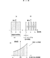
第1実施例では、参照信号周波数と遅延時間の対応関係を示すテーブルが既に求まって遅延時間テーブル保存部72に登録されているものとして説明したが、第2実施例ではこのテーブルを作成し、しかる後、第1実施例と同様の方法で遅延時間を制御する。図2は遅延時間テーブル作成原理説明図である。装置の信号帯域を図2(A)に示すようにf0〜f3のFAであるとする。図2(B)に示す帯域幅FBで中心周波数がf0〜f3まで順次大きくなるトレーニング信号を装置に入力し、それぞれのトレーニング信号に対して相関値が最大となる遅延時間差を求め、プロットすれば図2(C)に示す周波数−遅延特性が得られる。なお、トレーニング信号は装置の信号帯域に対し狭帯域な信号を用いるものとし、装置信号の帯域をFA、トレーニング信号帯域をFBとするとFA ≧FB が成り立つ。
図3は第2実施例の適応制御装置の構成図であり、図1の第1実施例と同一部分には同一符号を付している。異なる点は、通信制御部59、スイッチ60、遅延時間テーブル作成部76などの遅延時間テーブルを作成するための構成が追加された点である。尚、遅延部51cは図1の遅延部51cと同一の構成を有している。
送信信号を送信するに先立って、遅延時間テーブルを作成する。通信制御部59はスイッチ60によりトレーニング信号を選択するように制御し、且つ、遅延時間制御部51eに遅延時間テーブルを作成するよう指示する。ついで、通信制御部59は中心周波数f0の第1のトレーニング信号を発生すると共に、該中心周波数f0を遅延時間テーブル作成部76に入力する。
遅延時間設定部74は、最大相関を求めるために、遅延部51cの第2のセレクタ63(図1参照)を制御してフィードバック信号y(t)を取り出すシフトレジスタ61のシフト位置を切り替え、これによりフィードバック信号の遅延時間を変更する。そして、遅延時間設定部74は、各遅延時間において相関器75で演算した相関値を保存し、相関値が最大となる遅延時間を求め、この遅延時間を遅延時間テーブル作成部76に入力する。遅延時間テーブル作成部76は入力された遅延時間を中心周波数f0に対応させて記憶する。以後、通信制御部59は、周波数がf0からf3まで順次増大するように狭帯域のトレーニング信号を発生し、遅延時間テーブル作成部76は前記と同様に得られた遅延時間を周波数に対応させて記憶し、全帯域について周波数−遅延時間が求まれば遅延時間テーブル72に設定してテーブルの作成処理が完了する。これにより、通信制御部59はスイッチにより送信信号を選択させる。以後、第1実施例と同様に遅延時間制御及び適応制御が行われる。
(C)第3実施例
第1、第2実施例は参照信号周波数と遅延時間の対応をテーブル化し、該テーブルより遅延時間を求めて遅延部に設定する方式であるが、数点の周波数と遅延時間の対応を記憶し、それぞれの間を直線化して1次方程式で表現し、計算により遅延時間を求めて遅延部に設定するようにもできる。
図4は、第3実施例の説明図であり、トレーニング信号の中心周波数をf0 、0 、f3 と変化させ、この中心周波数の時に、フィードバック信号の遅延時間(遅延量)を求めて記憶する。そして、求めた3組の中心周波数と遅延量を用いて、中心周波数と遅延量の1 次方程式(A0×frq+B0,A1×frq+B1)を2つ生成し、参照信号周波数が変更した時、所定の方程式より参照信号周波数に応じた遅延量を求めて遅延部に設定する。
図5は第3実施例の適応制御装置の構成図であり、図1の第1実施例と同一部分には同一符号を付している。第1実施例と異なる点は、遅延時間計算部77を設けて遅延時間を計算により算出する点である。なお、送信信号を送信するに先立って、図3に示す方法でトレーニング信号を入力して幾つかの周波数に応じた遅延量を求めて遅延時間計算部77に入力しておく。
かかる状態において、送信信号が入力すると、適応制御部51dは、参照信号x(t)に適応制御結果を反映することにより得られた信号を変調部52に入力し、変調部52は入力信号に変調処理を施し、DA変換器53は変調信号をアナログ信号に変換して電力増幅器54に入力し、電力増幅器54は入力信号を増幅してアンテナ55より空間に放射する。方向結合器56は電力増幅器出力の一部分を取り出してAD変換器57を介して復調部58に入力し、復調部58は入力信号に復調処理を施して適応制御装置51に入力する。
又、送信信号が入力すると、周波数検出部71は参照信号の周波数成分を検出して遅延時間計算部77に入力する。遅延時間計算部77は参照信号の周波数成分が属する範囲に応じた一次方程式を用いて遅延時間を計算し、該遅延時間を遅延時間設定部74に入力する。遅延時間設定部74は、遅延時間計算部77から入力された遅延時間を遅延部51cの第1セレクタ62に初期設定する。
この結果、フィードバック信号y(t)は、設定された遅延時間だけ遅延部51cで遅延し、フィードバック信号の全遅延時間は、参照信号x(t)が遅延部51bを介して誤差演算部51aに到達するまでの全遅延時間と略等しくなる。
誤差演算部51aは遅延部51b,51cを介して入力する参照信号x′(t)とフィードバック信号y′(t)の差e(t)を演算し、適応制御部1dは該差e(t)が小さくなるように適応制御し、次の参照信号に適応制御結果を反映する。以後上記動作が繰り返される。以上の制御により、参照信号とフィードバック信号の遅延時間を等しくできるため良好な適応制御が可能となる。
又、以上と並行して第1実施例と同様の方法で遅延時間の微調整を行う。すなわち、遅延時間設定部74は、最大相関を求めるために、遅延部51cの第2のセレクタ63(図1参照)を制御してフィードバック信号y(t)を取り出すシフトレジスタ61のシフト位置を切り替え、これによりフィードバック信号の遅延時間を変更する。そして、遅延時間設定部74は、各遅延時間においてスライディング相関器75で演算した相関値を保存し、相関値が最大となる遅延時間を求め、この遅延時間を遅延部51cの第1のセレクタ63に再設定する。
最大相関を求める際のシフト範囲は初期設定した遅延時間の前後わずかな範囲でよく、これにより、遅延部51cの遅延時間をすばやくリアルタイムに微調整してフィードバック信号と参照信号の誤差演算部への到達時間を高精度に一致させることができ、良好な適応制御が可能となる。
(D)第4実施例
第1〜第3実施例はシングルキャリアで送信する場合であるが、マルチキャリア信号を用いて送信する場合がある。かかる場合、図6に示すようにキャリア数(使用帯域幅に相当)及びキャリア配置により特定される中心周波数に応じてフィードバック信号y(t)の遅延時間が変化する。そこで、第4実施例では、予め、キャリア数とキャリア配置の組み合わせ、あるいは中心周波数に対応させて遅延時間を測定して遅延時間テーブル保存部に登録しておき、実際のキャリア数とキャリア配置の組み合わせ、あるいは中心周波数に対応する遅延時間を該テーブルより求めて遅延部に設定する。
図7は第4実施例の構成図であり、図1の第1実施例と同一部分には同一符号を付している。第1実施例と異なる点は、
(1)n個(図ではn=4)の周波数を多重して送信する点(マルチキャリア送信)、
(2)キャリア数とキャリア配置の組み合わせ、あるいはキャリア数とキャリア配置により特定される中心周波数に対応させて遅延時間を保持する遅延時間テーブルを遅延時間テーブル保存部72に登録している点、
(3)遅延時間取得部73が通信制御部59からキャリア数とキャリア配置の組み合わせ、あるいは前記中心周波数を入手し、これらに対応する遅延時間を遅延時間テーブルより取得して遅延時間設定部74に入力する点、
である。尚、遅延部51cは図1の遅延部51cと同一の構成を有している。
周波数発生部65a〜65dは通信制御部59の制御でオン/オフされ、それぞれexp(jω1t)〜exp(jω4t)(ωn=2πt)の周波数信号を発生する。
この状態で各送信信号x1(t)〜x4(t)が入力すると、周波数シフト部66a〜66dはディジタルの各送信信号x1(t)〜x4(t)にexp(jω1t)〜exp(jω4t)(ωn=2πfn)を乗算して周波数f1〜f4に周波数シフトし、合成部67は周波数多重する。このディジタル周波数多重送信信号x(t)はシングルキャリアの送信信号x(t)に対応し、以後、シングルキャリアの場合と同様の適応制御、遅延時間制御を施される。
適応制御部51dは、送信信号x(t)に適応制御結果を反映することにより得られた信号を変調部52に入力し、変調部52は入力信号に変調処理を施し、DA変換器53は変調信号をアナログ信号に変換して電力増幅器54に入力し、電力増幅器54は入力信号を増幅してアンテナ55より空間に放射する。方向結合器56は電力増幅器出力の一部分を取り出してAD変換器57を介して復調部58に入力し、復調部58は入力信号に復調処理を施して適応制御装置51に入力する。
また、遅延時間取得部73は、通信制御部59からキャリア数とキャリア配置の組み合わせ、あるいはキャリア数とキャリア配置により特定される中心周波数を入手する。ついで、遅延時間取得部73は、入手したキャリア数とキャリア配置の組み合わせ、あるいは中心周波数に対応する遅延時間を遅延時間テーブル保存部72より取得して遅延時間設定部74に入力する。遅延時間設定部74は、遅延時間取得部73から入力された遅延時間を遅延部51cの第1セレクタ62(図1参照)に初期設定する。この結果、フィードバック信号y(t)は、設定された遅延時間だけ遅延部51cで遅延して誤差演算部51aに到達する。これにより、フィードバック信号の全遅延時間は、参照信号である送信信号x(t)が遅延部51bを介して誤差演算部51aに到達するまでの全遅延時間と略等しくなる。
誤差演算部51aは遅延部51b,51cを介して入力する参照信号x′(t)とフィードバック信号y′(t)の差e(t)を演算し、適応制御部51dは該差e(t)が小さくなるように適応制御し、次の送信信号に適応制御結果を反映する。以後上記動作が繰り返される。以上の制御により、参照信号とフィードバック信号の遅延時間を等しくできるため良好な適応制御が可能となる。
又、以上と並行して第1実施例と同様の方法で遅延時間の微調整を行う。すなわち、遅延時間設定部74は、最大相関を求めるために、遅延部51cの第2のセレクタ63(図1参照)を制御してフィードバック信号y(t)を取り出すシフトレジスタ61のシフト位置を切り替え、これによりフィードバック信号の遅延時間を変更する。そして、遅延時間設定部74は、各遅延時間において相関器75で演算した相関値を保存し、相関値が最大となる遅延時間を求め、この遅延時間を遅延部51cの第1のセレクタ63に再設定する。最大相関を求める際のシフト範囲は初期設定した遅延時間の前後わずかな範囲でよく、これにより、遅延部51cの遅延時間をすばやくリアルタイムに微調整してフィードバック信号と参照信号の誤差演算部への到達時間を高精度に一致させることができ、良好な適応制御が可能となる。
以上では、テーブルより遅延時間を取得したが、第3実施例と同様に、キャリア数、キャリア配置より遅延時間を演算する計算式を用いて遅延時間を取得することもできる。例えば、離散的にマルチキャリアの中心周波数に対応する遅延量を求めておき、これらを用いて中心周波数から遅延量を計算する計算式を確立し、実際のキャリア数、キャリア配置より中心周波数を求め、前記計算式を用いて遅延量を計算する。
(E)第5実施例
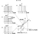
フィードバック信号の遅延時間は、キャリア数及びキャリア配置により変化すると共に、各キャリアの電力にも依存して変化する。図8においてAはキャリアの中心周波数と遅延量の関係を示す特性曲線、Bは電力と遅延量の関係を示す特性曲線である。キャリア数は同じであるが、電力が異なる(1)、(2)の遅延量を比べると中心周波数より高域側f2,f3の電力が小さい(2)の遅延量が少なくなっている。そこで、第5実施例では、キャリア数およびキャリア配置の組合わせ、あるいはこれらにより特定される中心周波数に対応する遅延量を示す第1のテーブルと、中心周波数より高域側の電力と低域側の電力との比(=高域側電力/低域側電力)に対応する遅延量の増減を示す第2のテーブルを用意し、これらテーブルより遅延量を取得するようにしている。図9を参照すると、曲線Bは第2のテーブルの電力比/遅延量増減割合特性である。電力比がr0であれば、増減割合が−α0となるから、第1のテーブルより求まる遅延時間をτとすれば、電力を考慮した時の遅延時間はτ(1−α0)となる。
図10は第5実施例の適応制御装置の構成図であり、図7の第4実施例と同一部分には同一符号を付している。異なる点は、
(1)遅延時間テーブル保存部72に上記第1、第2の2つのテーブルが登録されている点、
(2)各キャリアの電力を測定する電力測定部81が設けられている点、
(3)遅延時間取得部73が、上記第1、第2の2つのテーブルに基づいて遅延時間を取得する点である。
すなわち、遅延時間取得部73は、通信制御部59からキャリア数とキャリア配置の組み合わせ、あるいはキャリア数とキャリア配置より求まる中心周波数を入手し、これらに対応する遅延時間τを第1テーブルより取得する。ついで、遅延時間取得部73は、各キャリアの電力に基づいて高域側電力と低域側電力の電力比を計算し、該電力比に応じた遅延量増減割合αを第2のテーブルより求め、次式
τ(1+α)
により電力を考慮した遅延時間を求め、遅延時間設定部74に設定する。遅延時間設定部74は、遅延時間取得部73から入力された遅延時間を遅延部51cの第1セレクタ62(図1参照)に初期設定する。この結果、フィードバック信号y(t)は、設定された遅延時間だけ遅延部51cで遅延して誤差演算部51aに到達する。これにより、フィードバック信号の全遅延時間は、参照信号である送信信号x(t)が遅延部51bを介して誤差演算部51aに到達するまでの全遅延時間と略等しくなる。
(F)第6実施例
フィードバック信号の遅延時間は、キャリア数及びキャリア配置により変化すると共に、装置内温度にも依存して変化する。図11においてAはキャリアの中心周波数と遅延量の関係を示す特性曲線、Bは装置内温度と遅延量の関係を示す特性曲線であり、図12は温度T0における温度と遅延量の関係を示す特性曲線である。図11、図12より温度が上昇すると遅延時間が増大し、温度が下がると遅延時間が減少する。そこで、第6実施例では、キャリア数およびキャリア配置の組合わせ、あるいはこれらにより特定される中心周波数に対応する遅延量を示す第1のテーブルと、温度に対応する遅延量の増減量を示す第2のテーブルを用意し、これらテーブルより遅延量を取得するようにしている。
図13は第6実施例の適応制御装置の構成図であり、図7の第4実施例と同一部分には同一符号を付している。異なる点は、
(4)遅延時間テーブル保存部72に上記第1、第2の2つのテーブルが登録されてい
る点、
(5)装置内の温度を測定する温度センサー82が設けられている点、
(6)遅延時間取得部73が、キャリア数およびキャリア配置の組合わせ、あるいは
これらにより特定される中心周波数と、装置内温度とに基づいて遅延時間を
取得する点である。
すなわち、遅延時間取得部73は、通信制御部59からキャリア数とキャリア配置の組み合わせ、あるいはキャリア数とキャリア配置により特定される中心周波数を入手し、これらに対応する遅延時間τを第1テーブルより取得する。ついで、遅延時間取得部73は、装置内温度に応じた遅延量の増減量βを第2のテーブルより求め、次式
τ+β
により装置内温度を考慮した遅延時間を求め、遅延時間設定部74に設定する。遅延時間設定部74は、遅延時間取得部73から入力された遅延時間を遅延部51cの第1セレクタ62(図1参照)に初期設定する。この結果、フィードバック信号y(t)は、設定された遅延時間だけ遅延部51cで遅延して誤差演算部51aに到達する。これにより、フィードバック信号の全遅延時間は、参照信号である送信信号x(t)が遅延部51bを介して誤差演算部51aに到達するまでの全遅延時間と略等しくなる。
(G)第7実施例
フィードバック信号の遅延時間は、キャリア周波数に依存して変化する。図14はキャリア周波数と遅延時間の関係図であり、キャリア周波数が高くなると遅延量が増大する。そこで、第7実施例ではキャリア周波数と遅延時間の対応をテーブル化しておき、実際のキャリア周波数に応じた遅延時間をテーブルより求めて遅延部に設定するようにしている。
図15は第7実施例の構成図であり、図1の第1実施例と同一部分には同一符号を付している。第1実施例と異なる点は、
(1)キャリア周波数と遅延時間の対応テーブルを遅延時間テーブル保存部72に登
録している点、
(2)遅延時間取得部73が通信制御部59からキャリア周波数を入手し、該キャリア
周波数に対応する遅延時間を遅延時間テーブルより取得して遅延時間設定部
74に入力する点、
(3)べースバンド信号をRF信号に周波数変換する周波数変換部83,85,及びRF信号
をべースバンド信号に周波数変換する周波数変換部84,86に設定する制御信
号情報を用いている点、
である。尚、遅延部51cは図1の遅延部51cと同一の構成を有している。
送信信号が入力すると、適応制御部51dは、参照信号x(t)に適応制御結果を反映することにより得られた信号を変調部52に入力し、変調部52は入力信号に変調処理を施し、DA変換器53は変調信号をアナログ信号に変換する。周波数変換部の発振器83は通信制御部59から指示されたキャリア周波数で発振し、乗算器85はDA変換器から出力するべースバンド信号にキャリア周波数信号を乗算して無線信号に周波数変換し、該無線信号を電力増幅器54に入力し、電力増幅器54は入力信号を増幅してアンテナ55より空間に放射する。
方向結合器56は電力増幅器出力の一部分を取り出し、乗算器86は無線信号に発振器84から発生するキャリア周波数信号を乗算してべースバンド信号に周波数変換する。AD変換器57は乗算器86から出力するべースバンド信号をディジタル信号に変換して復調部58に入力し、復調部58は入力信号に復調処理を施して適応制御装置51に入力する。
一方、遅延時間取得部73は通信制御部59よりキャリア周波数を求め、遅延時間テーブル保存部72よりキャリア周波数に応じた遅延時間を取得し、遅延時間設定部74に入力する。遅延時間設定部74は、遅延時間取得部73から入力された遅延時間を遅延部51cの第1セレクタ62(図1参照)に初期設定する。この結果、フィードバック信号y(t)は、設定された遅延時間、遅延部51cで遅延して誤差演算部51aに到達する。これにより、誤差演算部51aに到達するまでのフィードバック信号の全遅延時間は、参照信号x(t)が遅延部51bを介して誤差演算部51aに到達するまでの全遅延時間と略等しくなる。
誤差演算部51aは遅延部51b,51cを介して入力する参照信号x′(t)とフィードバック信号y′(t)の差e(t)を演算し、適応制御部51dは該差e(t)が小さくなるように適応制御し、次の参照信号に適応制御結果を反映する。以後上記動作が繰り返される。以上の制御により、良好な適応制御が可能となる。
又、以上と並行して遅延時間の微調整を行う。すなわち、遅延時間設定部74は、最大相関を求めるために、遅延部51cの第2のセレクタ63(図1参照)を制御してフィードバック信号y(t)を取り出すシフトレジスタ61のシフト位置を切り替え、これによりフィードバック信号の遅延時間を変更する。そして、遅延時間設定部74は、各遅延時間においてスライディング相関器75で演算した相関値を保存し、相関値が最大となる遅延時間を求め、この遅延時間を遅延部51cの第1のセレクタ63に再設定する。
最大相関を求める際のシフト範囲は初期設定した遅延時間の前後わずかな範囲でよく、これにより、遅延部51cの遅延時間をすばやくリアルタイムに微調整してフィードバック信号と参照信号の誤差演算部への到達時間を高精度に一致させることができ、良好な適応制御が可能となる。
(H)第8実施例
以上の実施例では、参照信号およびフィードバック信号が誤差演算部に入力するまでの遅延時間の差を求めて遅延部に設定して該差が零となるように制御するものであるが、予め、参照信号周波数に対する遅延時間差特性を作成し、その逆特性を複素フィルタに設定して遅延時間差が零となるように制御することもできる。
図16は第8実施例の適応制御装置の構成図であり、図1の第1実施例と同一部分には同一符号を付している。異なる点は、
(1)フィードバック信号y(t)に遅延時間特性をキャンセルするための処理を施し
て誤差演算部51aに入力する複素フィルタ51fを設けた点
(2)通信制御部59、スイッチ60、遅延時間特性作成部91などの遅延時間特性を作
成するための構成が追加された点、
(3)遅延時間特性と逆特性を作成する逆特性作成部92を設けた点、
(4)該逆特性をフィードバック信号に付加するように係数を決定して複素フィル
タ51fに設定する複素フィルタ係数決定部93を設けた点、
である。尚、遅延部51cは図1の遅延部51cと同一の構成を有している。
図17は複素フィルタの構成図である。図16では明確に示していないが送信信号、フィードバック信号は複素信号である。複素フィルタ51fは、4つのFIRフィルタ101〜104と、加算器105,106で構成され、FIRフィルタ101、103にフィードバック信号の実数部が入力し、FIRフィルタ102、104にフィードバック信号の虚数部が入力する。加算器105はFIRフィルタ101、102の出力を合成して実数部を出力し、加算器106はFIRフィルタ103、104の出力を合成して虚数部を出力する。FIRフィルタ101、104の係数は同じでCn(n=1〜N)、FIRフィルタ102、103の係数は同じでDn(n=1〜N)であり、加算器105,106より
Σ(Ren+jIMn)×(Cn+jDn)
が出力される。複素フィルタ51fの係数により、入力信号に所定の遅延特性を付与することができる。
送信信号を送信するに先立って、複素フィルタ係数を決定して複素フィルタ51fに設定する。すなわち、第2実施例と同様に、通信制御部59はスイッチ60にトレーニング信号を選択させるよう制御し、且つ、遅延時間制御部51eに遅延時間特性を作成するよう指示する。ついで、通信制御部59は中心周波数f0の第1のトレーニング信号(図2参照)を発生すると共に、該中心周波数f0を遅延時間特性作成部91に入力する。尚、遅延特性取得時、複素フィルタ51fを遅延特性フラット、虚部係数0のフィルタとなるように設定する。
遅延時間設定部74は、最大相関を求めるために、遅延部51cの第2のセレクタ63(図1参照)を制御してフィードバック信号y(t)を取り出すシフトレジスタ61のシフト位置を切り替え、これによりフィードバック信号の遅延時間を変更する。そして、遅延時間設定部74は、各遅延時間において相関器75で演算した相関値を保存し、相関値が最大となる遅延時間を求め、この遅延時間を遅延時間特性作成部91に入力する。遅延時間特性作成部91は入力された遅延時間を中心周波数f0に対応させて記憶する。
以後、通信制御部59は、周波数がf0からf3まで順次増大するように狭帯域のトレーニング信号を発生し、遅延時間特性作成部91は前記と同様に遅延時間を周波数に対応させて記憶して遅延時間特性を作成する。これにより、図18(B)に示す遅延時間特性が得られる。ついで、逆特性作成部92は図18(C)に示すように 遅延時間特性と逆特性を作成し、複素フィルタ係数決定部93は該逆特性を示すように複素フィルタ51fのフィルタ係数を決定して該複素フィルタ51fに設定する。
複素フィルタの設定が完了すれば、通信制御部59はスイッチ60により入力信号を適応制御装置に入力させる。
送信信号が入力すると、適応制御部51dは、送信信号x(t)に適応制御結果を反映し、変調部52は適応制御を反映された信号に変調処理を施し、DA変換器53は変調信号をアナログ信号に変換して電力増幅器54に入力し、電力増幅器54は入力信号を増幅してアンテナ55より空間に放射する。
方向結合器56は電力増幅器出力の一部分を検出し、AD変換器57は検出信号をディジタル信号に変換して復調部58に入力し、復調部58は入力信号に復調処理を施して適応制御装置51に入力する。
適応制御装置の複素フィルタ51fは遅延時間差が零となるようにフィードバック信号にフィルタリング処理を施す。誤差演算部51aは遅延部51b,複素フィルタ51fを介して入力する参照信号x′(t)とフィードバック信号y′(t)の差e(t)を演算し、適応制御部1dは該差e(t)が小さくなるように適応制御し、次の参照信号に適応制御結果を反映する。以後上記動作が繰り返される。以上の制御により、良好な適応制御が可能となる。
以上では送信装置における電力増幅器で発生する歪補償する場合に適用した例を示したが本発明はかかる場合に限らず、適応制御により騒音を減少する場合などに適用できる。
又、以上では相関器としてスライディング相関器を用いた例を示したが、マッチトフィルタを用いて相関器を構成することができる。
(A) First Embodiment FIG. 1 is a block diagram of an adaptive control apparatus according to a first embodiment, which is an example applied to the case of compensating for distortion of a power amplifier.
The
The
The delay
The
The delay
The sliding
The overall operation will be described below.
When the transmission signal is input, the
When the transmission signal is input, the
The
In parallel with the above, the delay time is finely adjusted. That is, in order to obtain the maximum correlation, the delay
The shift range for obtaining the maximum correlation may be a slight range before and after the initially set delay time, which allows the delay time of the
(B) Second Embodiment In the first embodiment, it has been described that a table indicating the correspondence between the reference signal frequency and the delay time has already been obtained and registered in the delay time
FIG. 3 is a block diagram of the adaptive control apparatus according to the second embodiment, in which components identical with those of the first embodiment of FIG. The difference is that a configuration for creating a delay time table such as the
Prior to transmitting the transmission signal, a delay time table is created. The
The delay
(C) Third Embodiment In the first and second embodiments, the correspondence between the reference signal frequency and the delay time is tabulated, and the delay time is obtained from the table and set in the delay unit. It is also possible to store the correspondence of the delay time, linearize the interval between them and express it as a linear equation, and obtain the delay time by calculation and set it in the delay unit.
FIG. 4 is an explanatory diagram of the third embodiment. The center frequency of the training signal is changed to f0, 0 and f3, and the delay time (delay amount) of the feedback signal is obtained and stored at this center frequency. Then, using the obtained three sets of center frequency and delay amount, generate two linear equations (A 0 × frq + B 0 , A 1 × frq + B 1 ) of the center frequency and delay amount, and the reference signal When the frequency is changed, a delay amount corresponding to the reference signal frequency is obtained from a predetermined equation and set in the delay unit.
FIG. 5 is a block diagram of the adaptive control apparatus according to the third embodiment. Components identical with those of the first embodiment shown in FIG. The difference from the first embodiment is that a delay
In this state, when a transmission signal is input, the
When the transmission signal is input, the
As a result, the feedback signal y (t) is delayed by the
The
In parallel with the above, the delay time is finely adjusted by the same method as in the first embodiment. That is, the delay
The shift range for obtaining the maximum correlation may be a slight range before and after the initially set delay time, which allows the delay time of the
(D) Fourth Embodiment In the first to third embodiments, transmission is performed using a single carrier, but there are cases where transmission is performed using a multicarrier signal. In such a case, as shown in FIG. 6, the delay time of the feedback signal y (t) changes according to the number of carriers (corresponding to the used bandwidth) and the center frequency specified by the carrier arrangement. Therefore, in the fourth embodiment, the delay time is measured and registered in advance in the delay time table storage unit corresponding to the combination of the number of carriers and the carrier arrangement, or the center frequency, and the actual number of carriers and the carrier arrangement are determined. The delay time corresponding to the combination or center frequency is obtained from the table and set in the delay unit.
FIG. 7 is a block diagram of the fourth embodiment, and the same reference numerals are given to the same parts as those of the first embodiment of FIG. The difference from the first embodiment is that
(1) A point where n (n = 4 in the figure) frequencies are multiplexed and transmitted (multicarrier transmission),
(2) A combination of the number of carriers and the carrier arrangement, or a delay time table that holds a delay time corresponding to the center frequency specified by the number of carriers and the carrier arrangement is registered in the delay time
(3) The delay
It is. The
The
When the transmission signals x 1 (t) to x 4 (t) are input in this state, the
The
Also, the delay
The
In parallel with the above, the delay time is finely adjusted by the same method as in the first embodiment. That is, the delay
In the above, the delay time is acquired from the table. However, as in the third embodiment, the delay time can also be acquired using a calculation formula for calculating the delay time from the number of carriers and the carrier arrangement. For example, the delay amount corresponding to the center frequency of the multicarrier is obtained discretely, and a calculation formula for calculating the delay amount from the center frequency using these is established, and the center frequency is obtained from the actual number of carriers and the carrier arrangement. The delay amount is calculated using the above formula.
(E) Fifth Embodiment The delay time of the feedback signal varies depending on the number of carriers and the carrier arrangement, and also varies depending on the power of each carrier. In FIG. 8, A is a characteristic curve showing the relationship between the center frequency of the carrier and the delay amount, and B is a characteristic curve showing the relationship between the power and the delay amount. Comparing the delay amounts of (1) and (2) with the same number of carriers but different powers, the delay amount of (2) where the power on the high frequency side f2 and f3 is smaller than the center frequency is small. Therefore, in the fifth embodiment, a combination of the number of carriers and a carrier arrangement, or a first table showing a delay amount corresponding to the center frequency specified by these, power on the higher frequency side and lower frequency side than the center frequency A second table showing the increase / decrease of the delay amount corresponding to the ratio to the power (= high band side power / low band side power) is prepared, and the delay amount is obtained from these tables. Referring to FIG. 9, curve B represents the power ratio / delay amount increase / decrease ratio characteristic of the second table. If the power ratio is r0, the increase / decrease rate is -α0. Therefore, if the delay time obtained from the first table is τ, the delay time when power is taken into consideration is τ (1-α0).
FIG. 10 is a block diagram of the adaptive control apparatus according to the fifth embodiment. Components identical with those of the fourth embodiment shown in FIG. The difference is
(1) The first and second two tables are registered in the delay time
(2) A
(3) The delay
That is, the delay
Thus, the delay time considering the power is obtained and set in the delay
(F) Sixth Embodiment The delay time of the feedback signal varies depending on the number of carriers and the carrier arrangement, and also varies depending on the temperature in the apparatus. 11, A is a characteristic curve showing the relationship between the center frequency of the carrier and the delay amount, B is a characteristic curve showing the relationship between the temperature in the apparatus and the delay amount, and FIG. 12 shows the relationship between the temperature and the delay amount at the temperature T0. It is a characteristic curve. 11 and 12, the delay time increases as the temperature rises, and the delay time decreases as the temperature falls. Therefore, in the sixth embodiment, the first table indicating the delay amount corresponding to the combination of the number of carriers and the carrier arrangement, or the center frequency specified by these, and the increase / decrease amount of the delay amount corresponding to the temperature. Two tables are prepared, and the delay amount is obtained from these tables.
FIG. 13 is a block diagram of the adaptive control apparatus according to the sixth embodiment. Components identical with those of the fourth embodiment shown in FIG. 7 are designated by like reference characters. The difference is
(4) The first and second tables are registered in the delay time
(5) A
(6) The delay
That is, the delay
Thus, the delay time considering the temperature in the apparatus is obtained and set in the delay
(G) Seventh Embodiment The delay time of the feedback signal varies depending on the carrier frequency. FIG. 14 is a diagram showing the relationship between the carrier frequency and the delay time. As the carrier frequency increases, the delay amount increases. Therefore, in the seventh embodiment, the correspondence between the carrier frequency and the delay time is tabulated, and the delay time corresponding to the actual carrier frequency is obtained from the table and set in the delay unit.
FIG. 15 is a block diagram of the seventh embodiment, and the same reference numerals are given to the same parts as those of the first embodiment of FIG. The difference from the first embodiment is that
(1) The correspondence table of carrier frequency and delay time is registered in the delay time
(2) Delay
Point to enter in 74,
(3) The control signal information set in the
It is. The
When the transmission signal is input, the
The
On the other hand, the delay
The
In parallel with the above, the delay time is finely adjusted. That is, the delay
The shift range for obtaining the maximum correlation may be a slight range before and after the initially set delay time, which allows the delay time of the
(H) Eighth Embodiment In the above embodiment, a difference in delay time until the reference signal and the feedback signal are input to the error calculation unit is obtained, set in the delay unit, and controlled so that the difference becomes zero. However, it is also possible to create a delay time difference characteristic with respect to the reference signal frequency in advance and set the inverse characteristic of the complex filter to control the delay time difference to be zero.
FIG. 16 is a block diagram of the adaptive control apparatus of the eighth embodiment, where the same reference numerals are given to the same parts as those of the first embodiment of FIG. The difference is
(1) The feedback filter y (t) is provided with a
(2) Configurations for creating delay time characteristics such as
(3) Providing an inverse
(4) A complex filter
It is. The
FIG. 17 is a configuration diagram of a complex filter. Although not clearly shown in FIG. 16, the transmission signal and the feedback signal are complex signals. The
Is output. A predetermined delay characteristic can be given to the input signal by the coefficient of the
Prior to transmitting the transmission signal, complex filter coefficients are determined and set in the
The delay
Thereafter, the
When the setting of the complex filter is completed, the
When the transmission signal is input, the
The
The
Although the example applied to the case where the distortion generated in the power amplifier in the transmission apparatus is compensated has been described above, the present invention is not limited to such a case, and can be applied to the case where noise is reduced by adaptive control.
Moreover, although the example which used the sliding correlator as a correlator was shown above, a correlator can be comprised using a matched filter.
51 適応制御装置
51b,51c 遅延部
51d 適応制御部
51e 遅延時間制御部
52 変調部
53 DA変換器
54 電力増幅器
55 アンテナ
56 方向結合器
57 AD変換器
58 復調部
71 周波数検出部
72 遅延時間テーブル保存部
73 遅延時間取得部
74 遅延時間設定部
75 スライディング相関器
51 Adaptive controller
51b, 51c Delay part
51d Adaptive controller
51e Delay time controller
52 Modulator
53 DA converter
54 Power amplifier
55 Antenna
56 directional coupler
57 AD converter
58 Demodulator
71 Frequency detector
72 Delay time table storage
73 Delay time acquisition unit
74 Delay time setting section
75 sliding correlator
Claims (4)
参照信号とフィードバック信号が同時に前記演算部に入力するように少なくとも一方の信号を、設定された遅延時間だけ遅延する遅延部、
前記参照信号の周波数成分を検出する周波数成分検出部、
該周波数成分に基づいて前記遅延時間を取得する遅延時間取得部、
該取得した遅延時間を前記遅延部に設定する遅延時間設定部、
を備えたことを特徴とする適応制御装置。 In an adaptive control apparatus including an arithmetic unit that calculates a difference between a reference signal and a feedback signal, an adaptive control unit that adaptively controls the difference to reduce the difference and reflects the adaptive control result in the reference signal.
A delay unit that delays at least one signal by a set delay time so that a reference signal and a feedback signal are simultaneously input to the calculation unit;
A frequency component detector that detects a frequency component of the reference signal;
A delay time acquisition unit for acquiring the delay time based on the frequency component;
A delay time setting unit for setting the acquired delay time in the delay unit;
An adaptive control device comprising:
を備え、前記遅延時間設定部は該遅延時間差を前記遅延時間として前記遅延部に設定する、
ことを特徴とする請求項1記載の適応制御装置。 A delay time difference detection unit that measures a difference in delay time until a reference signal and a feedback signal are input to the calculation unit after setting the delay time in the delay unit;
The delay time setting unit sets the delay time difference as the delay time in the delay unit.
2. The adaptive control apparatus according to claim 1, wherein:
トレーニング信号である参照信号とフィードバック信号が前記演算部に入力するまでの遅延時間の差を測定する遅延時間差検出部、
トレーニング信号の中心周波数と前記測定した遅延時間差との対応テーブルを保存する保存部、
を備え、前記遅延時間取得部は前記検出した周波数成分に応じた遅延時間差を前記対応テーブルより取得し、前記遅延時間として遅延部に設定する、
ことを特徴とする請求項1記載の適応制御装置。 A training signal generator for outputting a plurality of training signals having different frequencies as reference signals;
A delay time difference detection unit that measures a difference in delay time until a reference signal that is a training signal and a feedback signal are input to the calculation unit;
A storage unit for storing a correspondence table between the center frequency of the training signal and the measured delay time difference;
The delay time acquisition unit acquires a delay time difference according to the detected frequency component from the correspondence table, and sets the delay time as the delay time in the delay unit.
2. The adaptive control apparatus according to claim 1, wherein:
ことを特徴とする請求項1記載の適応制御装置。 The delay time acquisition unit acquires a delay time according to the detected frequency using a calculation formula for calculating a delay time from a reference signal frequency.
2. The adaptive control apparatus according to claim 1, wherein:
Applications Claiming Priority (1)
| Application Number | Priority Date | Filing Date | Title |
|---|---|---|---|
| PCT/JP2002/005324 WO2003103164A1 (en) | 2002-05-31 | 2002-05-31 | Adaptive controller |
Related Child Applications (3)
| Application Number | Title | Priority Date | Filing Date |
|---|---|---|---|
| JP2006335480A Division JP4335250B2 (en) | 2006-12-13 | 2006-12-13 | Adaptive controller |
| JP2006335481A Division JP2007082264A (en) | 2006-12-13 | 2006-12-13 | Adaptive control apparatus |
| JP2006335479A Division JP4480711B2 (en) | 2006-12-13 | 2006-12-13 | Adaptive controller |
Publications (2)
| Publication Number | Publication Date |
|---|---|
| JPWO2003103164A1 JPWO2003103164A1 (en) | 2005-10-06 |
| JP3923978B2 true JP3923978B2 (en) | 2007-06-06 |
Family
ID=29606635
Family Applications (1)
| Application Number | Title | Priority Date | Filing Date |
|---|---|---|---|
| JP2004510127A Expired - Fee Related JP3923978B2 (en) | 2002-05-31 | 2002-05-31 | Adaptive controller |
Country Status (4)
| Country | Link |
|---|---|
| US (1) | US7496152B2 (en) |
| EP (1) | EP1511179B1 (en) |
| JP (1) | JP3923978B2 (en) |
| WO (1) | WO2003103164A1 (en) |
Families Citing this family (16)
| Publication number | Priority date | Publication date | Assignee | Title |
|---|---|---|---|---|
| JP4323968B2 (en) * | 2004-01-14 | 2009-09-02 | 株式会社日立コミュニケーションテクノロジー | Timing adjustment method for wireless communication device |
| CN101099296A (en) * | 2005-01-04 | 2008-01-02 | 富士通株式会社 | DC offset compensation method and device |
| US7542519B2 (en) * | 2005-12-29 | 2009-06-02 | Crestcom, Inc. | Radio frequency transmitter and method therefor |
| JP4388943B2 (en) * | 2006-10-23 | 2009-12-24 | Okiセミコンダクタ株式会社 | Correlator |
| JP2008205759A (en) * | 2007-02-20 | 2008-09-04 | Japan Radio Co Ltd | Distortion compensating device |
| EP2270993B1 (en) * | 2008-04-21 | 2018-07-11 | Nippon Telegraph and Telephone Corporation | Radio communication system and radio communication method |
| JP4721074B2 (en) * | 2008-04-23 | 2011-07-13 | ソニー株式会社 | Receiving apparatus, receiving method, and program |
| US7847646B2 (en) | 2008-05-27 | 2010-12-07 | Favepc, Inc. | Carrier generator with LC network |
| JP5251565B2 (en) * | 2009-02-05 | 2013-07-31 | 富士通株式会社 | Predistorter and delay adjustment method thereof |
| CN102640406A (en) * | 2009-12-15 | 2012-08-15 | 富士通株式会社 | Power supply device |
| US9128496B2 (en) * | 2011-10-26 | 2015-09-08 | The United States Of America As Represented By Secretary Of The Navy | Auto-ranging for time domain extraction of perturbations to sinusoidal oscillation |
| JP2015220739A (en) | 2014-05-21 | 2015-12-07 | 富士通株式会社 | Distortion compensation device and distortion compensation method |
| JP6311457B2 (en) * | 2014-05-30 | 2018-04-18 | 富士通株式会社 | Control device, DC-DC converter, switching power supply device, and information processing device |
| JP2016167781A (en) * | 2015-03-10 | 2016-09-15 | 富士通株式会社 | Radio communication device and method of controlling radio communication device |
| JP2017200147A (en) * | 2016-04-28 | 2017-11-02 | 富士通株式会社 | Radio equipment and coefficient update method |
| US11770145B2 (en) | 2021-08-27 | 2023-09-26 | Samsung Electronics Co., Ltd | System and method for efficient initialization of memory digital pre-distorter coefficients to reduce calibration time |
Family Cites Families (13)
| Publication number | Priority date | Publication date | Assignee | Title |
|---|---|---|---|---|
| US4217586A (en) * | 1977-05-16 | 1980-08-12 | General Electric Company | Channel estimating reference signal processor for communication system adaptive antennas |
| KR950000761B1 (en) * | 1992-01-15 | 1995-01-28 | 삼성전자 주식회사 | Apparatus for synchronizing serial input signals |
| JP3582809B2 (en) * | 1996-03-12 | 2004-10-27 | ローランド株式会社 | Effect device |
| US6133789A (en) * | 1997-12-10 | 2000-10-17 | Nortel Networks Corporation | Method and system for robustly linearizing a radio frequency power amplifier using vector feedback |
| JPH11202028A (en) * | 1998-01-14 | 1999-07-30 | Mitsubishi Electric Corp | Ic tester |
| JP4288777B2 (en) * | 1999-08-11 | 2009-07-01 | ソニー株式会社 | Multi-carrier signal transmitter and multi-carrier signal receiver |
| JP4014343B2 (en) * | 1999-12-28 | 2007-11-28 | 富士通株式会社 | Distortion compensation device |
| US6275106B1 (en) * | 2000-02-25 | 2001-08-14 | Spectrian Corporation | Spectral distortion monitor for controlling pre-distortion and feed-forward linearization of rf power amplifier |
| JP4326673B2 (en) * | 2000-06-06 | 2009-09-09 | 富士通株式会社 | Method for starting communication apparatus having nonlinear distortion compensation apparatus |
| WO2002017586A1 (en) | 2000-08-18 | 2002-02-28 | Nokia Corporation | Multicarrier transmitter circuit arrangement with predistortion linearisation method |
| JP2002077285A (en) * | 2000-08-31 | 2002-03-15 | Hitachi Kokusai Electric Inc | Transmiter |
| JP3752137B2 (en) | 2000-08-31 | 2006-03-08 | 三菱電機株式会社 | Data transmission apparatus and data transmission method |
| DE10054075A1 (en) * | 2000-10-31 | 2002-05-08 | Heidenhain Gmbh Dr Johannes | Position determination method and position measuring device |
-
2002
- 2002-05-31 JP JP2004510127A patent/JP3923978B2/en not_active Expired - Fee Related
- 2002-05-31 WO PCT/JP2002/005324 patent/WO2003103164A1/en active Application Filing
- 2002-05-31 EP EP02730824.6A patent/EP1511179B1/en not_active Expired - Fee Related
-
2004
- 2004-10-26 US US10/976,290 patent/US7496152B2/en not_active Expired - Fee Related
Also Published As
| Publication number | Publication date |
|---|---|
| US7496152B2 (en) | 2009-02-24 |
| US20050058220A1 (en) | 2005-03-17 |
| EP1511179A1 (en) | 2005-03-02 |
| EP1511179A4 (en) | 2006-10-04 |
| EP1511179B1 (en) | 2013-07-03 |
| WO2003103164A1 (en) | 2003-12-11 |
| JPWO2003103164A1 (en) | 2005-10-06 |
Similar Documents
| Publication | Publication Date | Title |
|---|---|---|
| JP3923978B2 (en) | Adaptive controller | |
| US6836517B2 (en) | Distortion compensating apparatus | |
| JP3844352B2 (en) | Transmitter | |
| JP3857652B2 (en) | Distortion compensation device | |
| US8442157B2 (en) | Wireless apparatus and signal processing method | |
| US20100194474A1 (en) | Predistorter and Distortion Compensation Method | |
| WO2011125261A1 (en) | Amplifier circuit and wireless communication device | |
| JP5376050B2 (en) | Cross-polarization interference compensation apparatus, cross-polarization interference compensation method, program, and phase estimation method | |
| JP4480711B2 (en) | Adaptive controller | |
| JP3439696B2 (en) | Transmission band limiting filter device and transmission device | |
| US8854128B2 (en) | Amplifying device and signal processing device | |
| JP4335250B2 (en) | Adaptive controller | |
| CN100512253C (en) | Multicarrier receiver and transmitter with delay correcting function | |
| US6614840B1 (en) | Equalizer with phase-locked loop | |
| JP2007082264A (en) | Adaptive control apparatus | |
| US7584410B2 (en) | Frequency error detector and combiner in receiving end of mobile communication system | |
| JP6056956B2 (en) | Communication apparatus and distortion suppression method thereof | |
| JP3559428B2 (en) | Receiver | |
| KR20000047582A (en) | Channel characteristics estimation apparatus | |
| JP3837058B2 (en) | Transmitter | |
| EP1855386A2 (en) | Adaptive control apparatus | |
| JP5572590B2 (en) | PHASE CHARACTERISTIC ESTIMATION DEVICE, PHASE CORRECTION DEVICE, SIGNAL GENERATING DEVICE, AND PHASE CHARACTERISTIC ESTIMATION METHOD INCLUDING THE SAME | |
| JP4024602B2 (en) | Sample rate converter and receiver using the same | |
| JPH098766A (en) | Quadrature frequency dividing multiplex receiver | |
| JP4226064B1 (en) | Radio signal demodulator |
Legal Events
| Date | Code | Title | Description |
|---|---|---|---|
| A131 | Notification of reasons for refusal |
Free format text: JAPANESE INTERMEDIATE CODE: A131 Effective date: 20061024 |
|
| A521 | Written amendment |
Free format text: JAPANESE INTERMEDIATE CODE: A523 Effective date: 20061213 |
|
| TRDD | Decision of grant or rejection written | ||
| A01 | Written decision to grant a patent or to grant a registration (utility model) |
Free format text: JAPANESE INTERMEDIATE CODE: A01 Effective date: 20070220 |
|
| A61 | First payment of annual fees (during grant procedure) |
Free format text: JAPANESE INTERMEDIATE CODE: A61 Effective date: 20070222 |
|
| R150 | Certificate of patent or registration of utility model |
Free format text: JAPANESE INTERMEDIATE CODE: R150 |
|
| FPAY | Renewal fee payment (event date is renewal date of database) |
Free format text: PAYMENT UNTIL: 20100302 Year of fee payment: 3 |
|
| FPAY | Renewal fee payment (event date is renewal date of database) |
Free format text: PAYMENT UNTIL: 20110302 Year of fee payment: 4 |
|
| FPAY | Renewal fee payment (event date is renewal date of database) |
Free format text: PAYMENT UNTIL: 20110302 Year of fee payment: 4 |
|
| FPAY | Renewal fee payment (event date is renewal date of database) |
Free format text: PAYMENT UNTIL: 20120302 Year of fee payment: 5 |
|
| FPAY | Renewal fee payment (event date is renewal date of database) |
Free format text: PAYMENT UNTIL: 20130302 Year of fee payment: 6 |
|
| FPAY | Renewal fee payment (event date is renewal date of database) |
Free format text: PAYMENT UNTIL: 20140302 Year of fee payment: 7 |
|
| LAPS | Cancellation because of no payment of annual fees |