Embodiment
[0011] below, according to description of drawings about various embodiments of the present invention.
[0012] all structures
Fig. 1 shows in an embodiment in the liquid crystal indicator in order to the structural drawing of supplying video data to pixel circuit.
[0013] at this embodiment, 6 the video line 10 whenever digital luminance signal of 64 color ranges (gradation) of each picture element transmits according to picture element clock (clock) order.Even, in fact have R (red), G (green), three video lines of B (indigo plant), and video of all kinds supply in parallel, be supplied to the picture element of corresponding look, but in accompanying drawing, only show 1 look.
[0014] input end of the switch 12 that video line 10 connections each row (column) of corresponding picture element are provided with.The control end of this switch 12 is connected with the output of horizontal transmission buffer (register) 14 separately.At this, horizontal transmission buffer 14, by with the synchronous picture element clock of sequential of each picture element of the video data that is supplied to video line, transmit horizontal start signal (STH) in regular turn, have buffer of each row of corresponding picture element.Even, in this explanation, show for setting forth about RGB color, show that position and picture element are same.In addition, be supplied in the transmission clock of horizontal transmission buffer, have the cycle of 2 times on general picture element clock, and the situation of 2 clocks (CKH, XCKH) of use inverted phase is more.
[0015] that is, when video line being supplied with the picture element video data of the 1st row, then horizontal start signal STH is inputed to first horizontal transmission buffer 14 and makes corresponding switch 12 conductings.And, in horizontal transmission buffer 14, transmit horizontal start signal (STH) in regular turn according to the picture element clock, just be supplied to the video data of each picture element of video line 10, make switch 12 conductings of corresponding its picture element in regular turn.Even switch 12 is with the mode structure of be connected in parallel p channel transistor (TFT) and n channel transistor (TFT), non-counter-rotating output conducting simultaneously of a buffer by horizontal transmission buffer 14 separately with counter-rotating output. cut off and move.
[0016] output terminal of each switch 12 is connected with the input end of 6 SRAM 16 separately, and the output terminal of these SRAM 16 is connected in the input end of 6 SRAM 18 separately.Thereby, be supplied in the video data of each picture element of video line 10 in regular turn, input to SRAM 16 by switch 12 sequential turn-on.And, input to the time point of SRAM 16 at the video data of 1 row (1 horizontal scanning line) part, the video data of 1 row part is sent to pairing SRAM 18 simultaneously separately, repeat this action in each each horizontal scan period.Thereby, in each horizontal scan period, 1 video data of going part is inputed to SRAM 16, afterwards this video data is sent to SRAM 18, the video data that is transmitted is maintained SRAM 18 in next horizontal scan period, and output thus.Then, repeat this action.
[0017] output terminal of SRAM18 is connected with the input end of digital analog converter (DAC) 20.This DAC 20 will become the analog video signal of 64 color ranges from the 6 digital video data-switching that SRAM 18 supplies with.Even, DAC 20 executions are changed towards the voltage of liquid crystal with predetermined period and are applied direction, just implement so-called AC and drive, and export 2 kinds of polarity (the common electrode current potential of Liquid crystal module is used as benchmark, the voltage of liquid crystal is applied direction become 2 opposite polarity) vision signal.As aftermentioned, in the present embodiment, as the mode of AC driving, owing to utilize some counter-rotating (dot reverse) mode, so in the picture element of level and vertical direction adjacency, counter-rotating is applied to the voltage direction of liquid crystal, reverses in per 1 news frame (frame) with regard to the liquid crystal of 1 picture element.
[0018] in addition, the output terminal of each DAC 20 is connected in the input end of amplifier (Amp) 22, and the output terminal of this amplifier 22 is connected to data line DL via change-over switch 24.This data line DL extends to row (vertical scanning direction), and 1 corresponding row pixel circuit 100 promptly is connected in this data line DL separately.Even in this example, data line DL is owing to being connected in the source electrode of the picture element TFT in the pixel circuit 100, so be also referred to as source electrode line (source line).
[0019] thereby, will be supplied to data line DL from the analog video signal of DAC20 output, and be input into the pixel circuit 100 that is equivalent to this journey, and carry out showing corresponding to the analog video signal that each picture element received.
[0020] SRAM structure
In present embodiment, have 2 SRAM 16,18 that keep 6 bit digital video datas in each row.In addition, video data, its dynamic range (dynamic range) is set for less, and as the data of input DAC20, the general requirement established dynamic range greatly.Therefore, for example, the 5V amplitude voltage is shifted (Level shift) to the 8V amplitude.
[0021] in the present embodiment, make up latch circuit (latch circuit) and voltage shift device and structure SRAM16, and also implement voltage shift (level shifting) in SRAM 16.
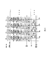
[0022] Fig. 2, expression shows the structure of the latch circuit (SRAM 18) that this SRAM 16 of latch-type voltage shift circuit (SRAM16) and breech lock of present embodiment exports.At this, video data is 6 a numerical data, only shows 1 part.
[0023] digital of digital video data with the 5V amplitude is applied to switch 610.This switch 610 is controlled by the clock of synchronous points clock (dot clock), and each shows that picture element (point) reads in the video data that is supplied to input end.For example, during switch 12 conductings of the corresponding video line 10 of Fig. 1, actuating switch 610 and inputting video data.At this moment, also switch 610 can be used as switch 12.
[0024] output terminal of switch 610 is connected with the 1st breech lock 620.The 1st breech lock 620 is the 5V amplitude, by 2 622,624 structures of reverser that are connected to each other the 5V action of exporting.In this embodiment, because the output of switch 610 is supplied to the input end of reverser 622, so reverse signal inputs to reverser 624.Thereby, according to the output state of switch 610, the input state of decision reverser 622, and a pair of outgoing side state of decision reverser 622.
[0025], in this embodiment, the ability of reverser 622 should be set as greater than reverser 624 at this.Whereby, even during the video data of counter-rotating input, so the reverser 622 that reverses easily is these data of energy breech lock.
The a pair of output (polarity is opposite) of [0026] the 1st breech lock 620 inputs to the voltage shift device 630 of voltage driven type.This voltage shift device 630 is arranged on 3 transistor institute structures that are connected in series between the VSS of the VDD of 8V and 0V by 2 of parallel connection configurations.
[0027] between VDD and the VSS, p channel TFT 632a, p channel TFT 634a and n channel TFT 636a that configuration is connected in series, and the p channel TFT 632b, the p channel TFT 634b that are connected in series and n channel TFT 636b.Also have, the grid of TFT 634a and TFT 636a is connected with switch 610 outputs by latch circuit 620 breech locks; And, supply with reverse signal by switch 610 outputs of latch circuit 620 breech locks to the grid of TFT634b and TFT 636b.In addition, the grid of TFT632a is connected to the intermediate point of TFT 634b and TFT 636b; And the grid of TFT 632b is connected to the intermediate point of TFT 634a and TFT 636a.
[0028] according to this structure, output according to breech lock 620, the grid of TFT 632a that is be TFT 634b and n channel TFT 636b intermediate point, TFT 632b grid that is be the intermediate point of TFT 634a and n channel TFT 636a, wherein any one party becomes H voltage, the opposing party becomes L voltage.For example, when switch 610 was output as H voltage ([1]), the intermediate point of TFT 634b and n channel TFT 636b became H voltage, and the intermediate point of TFT 634a and n channel TFT 636a becomes L voltage.
[0029] from the output of the intermediate point of the intermediate point of TFT 634b and n channel TFT 636b and TFT 634a and n channel TFT 636a, inputs to the 2nd breech lock 640.The 2nd breech lock 640 is by the reverser that is connected 642 and reverser 644 structures, the output that the output of TFT 634b and n channel TFT 636b intermediate point inputs to input, TFT 634a and the TFT636a intermediate point of reverser 642 inputs to the input of reverser 644, and the output of reverser 642 (input of reverser 644) becomes the output of the 2nd breech lock 640.
[0030] thereby, input to the data of switch 610, live by the 1st breech lock 620 breech locks, and by the signal of voltage shift device 630 voltage shift, the signal that is reversed by voltage shift is latched to the 2nd breech lock 640 as the signal of 8V.Even, the 1st breech lock 620, voltage shift device 630 and the 2nd breech lock 640 structure SRAM 16.Thereby, can obtain the 5V amplitude voltage is displaced to the signal of 8V in the output of SARM 16.So, latch circuit is set, can implements breech lock action and voltage shift action simultaneously by input side and outgoing side at voltage shift device 630.Thereby, compare with the situation that indivedual executions should be moved, can reduce consumes power.
The output of [0031] the 2nd breech lock 640 is by reverser 650 counter-rotatings.Even, during with the contrast of the structure of Fig. 1, the corresponding SRAM 16 of part till this reverser 650, whereby, the video data of being imported promptly is stored according to Dot Clock (dot clock), voltage shift and exporting.
[0032] output of reverser 650 is supplied to breech lock 670 via switch 660.The data of switch 660,1 horizontal scanning line parts are input into SRAM 16 backs and only open in the scheduled period.Breech lock 670 is formed with reverser 674 by being connected to each other the reverser of exporting 672, and the output of switch 660 is inputed to reverser 672, and its output becomes the output of breech lock 670.And the output of this breech lock 670 is by reverser 680 counter-rotatings and output.Thereby, breech lock 670 and reverser 680 structure SRAM 18.That is at 1 horizontal scanning line, the video data of each picture element is opened switch 660 in the stage that is stored to SRAM 16, and the video data of this moment is set to SRAM18.For example, during horizontal flyback (horizontal retrace), the blanket SRAM 18 that is sent to of the data of all SRAM 16.
[0033] like this, according to present embodiment, when SRAM 16 storage data, also can implement voltage shift.Therefore, can reach efficient action.
[0034] structure of the high-order position of DAC20 conversion
Fig. 3 shows the structure of the high-order position conversion of DAC20.Reference voltage generating circuit 300 has reference voltage amplifier 300a, 300b.The benchmark electric amplifier is pressed 300a, 300b, and both all cut apart supply voltage VCC and GND with 10 resistance of resistance R 0 to R9, and produces 9 reference voltages of v0 to v8. Reference voltage amplifier 300a, 300b are in per 1 horizontal scan period alternating movement.Thereby 9 reference voltage v0 to v8 are in per 1 horizontal period reversed polarity.That is in benchmark amplifier 300a when action,, v8 is near VCC voltage, and v0 is near GND voltage, and during benchmark amplifier 300b action, then becomes opposite.In addition, the benchmark amplifier 300a of per 1 horizontal period, the switching of 300b, FRP implements by signal.For example, benchmark amplifier 300a action when signal FRP is H voltage, and benchmark amplifier 300b action during L voltage.
[0035] data D5-D3 inputs to 4 code translators of top H side code translator 310, top L side code translator 312, bottom H side code translator 314, bottom L side code translator 316, and reference voltage v0 to v8 also is supplied to these code translators 310 to 316 separately.Top H side code translator 310,8 kinds according to 111 to 000, selection reference voltage v8 to v1 and output data D5 to D3; Top L side code translator 312 is according to 111 to 000 8 kinds, selection reference voltage v7 to v0 and output data D5 to D3.Thereby the output VH of top H side code translator 310 becomes the voltage (v8 is the situation of VCC side) than the output VL higher order section of top L side code translator 312.On the other hand, bottom H side code translator 314 is according to 111 to 000 8 kinds, selection reference voltage v0 to v7 and output data D5 to D3; Bottom L side code translator 316 is according to 111 to 000 8 kinds, selection reference voltage v1 to v8 and output data D5 to D3.Thereby the output VH of bottom H side code translator 314 becomes the voltage (v8 is the situation of VCC side) than a low stage of output VL of bottom L side code translator 316.
[0036] like this, top code translator 310,312, output only is offset output voltage V H, the VL of the voltage of corresponding D3 position.Bottom code translator 314,316, the polarity of counter-rotating top code translator 310,312 (with respect to the numerical data augment direction of input or reduce the change direction of direction, the simulating signal VH of output, VL are augment direction or the change direction that reduces direction); This point of voltage VH, VL of 1 part that bottom H side code translator 314 and bottom L side code translator 316, output are different from D3 is identical.
[0037] even, when the output of top code translator 310,312 is applied to the data line DL of odd column, the output of bottom code translator 314,316 is supplied to the data line DL of even column.
[0038] like this, by with top code translator 310,312 and bottom code translator 314,316, it is opposite that reference voltage is supplied with, and utilizes 1 reference voltage generating circuit 300, can be performed in the digital analogue conversion of the upper side of panel and lower side two sides' code translator.Thereby, with the output alternative supply of upper side code translator 310,312 and bottom code translator 314,316 to data line DL, can be with the polarity of vision signal with regard to each data line DL counter-rotating.More and, by being used alternatingly reference voltage amplifier 300a, 300b, can the polarity of the vision signal that is supplied to each data line DL be changed with regard to per 1 horizontal scanning line with regard to per 1 horizontal line.Thereby, can be achieved in the some inversion driving of liquid crystal indicator.Also have,, can use 1 reference voltage generating circuit 300 in the situation of implementing this driving, thus circuit can be simplified, and seek the low consumption electric weightization.
[0039] the low-order bit conversion of DAC20 and amplifier 22 structures
As above-mentioned, from 3 of high-orders (D5-when D3) obtaining VH, VL,, obtain voltage according to 8 kinds of D2-D0 about the voltage difference of VH, VL.Fig. 4 shows this structure.D2 is directly inputted into the grid of TFT 410-2 in the same old way, and counter-rotating and input to the grid of TFT 412-2.The termination of TFT 410-2 is supplied with by VH, and VL is supplied to the end of TFT 412-2.The other end of TFT 410-2,412-2 is controlled the end that TFT 420-2 is connected to electric capacity 430-2 via charging.The other end of electric capacity 430-2 is connected to ground connection.
[0040] thereby, when D2 is H voltage ([1]), TFT 410-2 conductings, and select VH.During charging control TFT 420-2 conductings, electric capacity 430 is charged by VH.On the other hand, D2 is L voltage ([0]), and electric capacity 430 is promptly charged by VL.
[0041], is arranged to essentially identical structure with D2 about D1, D0.Thereby VH or VL charge to corresponding electric capacity 430-1,430-0 according to the value of D1, D2.
[0042] more and, charging control TFT 420-r being set, this charging control TFT420-r extraneous data directly charges to corresponding electric capacity 430-r with VL.Even charging control TFT 420-r, 420-0,420-1,420-2 is by charging signals (Charge) conducting. cut off.
[0043] also have, electric capacity 430-r, 430-0,430-1,430-2 sets in the mode of its capacitance C, C, 2C, 4C.Even C is for example 0.5pF, this moment, 4C became 2pF.
[0044] more and, electric capacity 430-r, 430-0,430-1,430-2 upside, by 3 in conjunction with connecting with TFT440-1,440-2,440-3, the upside of electric capacity 430-r becomes output terminal via TFT440-r.
[0045] also have, binding signal (Combine) is supplied in conjunction with the grid with TFT440-1,440-2,440-3 and TFT440-r.
[0046] by sort circuit, as long as D2-D0 all is [0], electric capacity 430-2,430-1,430-0,430-r are all charged by VL.Thereby output voltage becomes VL.At this, VL such as above-mentioned by the value that D5-D3 selects, forms to by the specific voltage of D5-D0.
[0047] again and, as long as D0 be [1], (VH-VL) the especially many chargings of the electric charge of C promptly adds the voltage of its 1/8C in VL, and exports VL+ (VH-VL)/8.D2 is [1], and (the especially many chargings of the electric charge of VH-VL) 4 add the voltage of its 1/8C in VL and export VL+4 (VH-VL)/8.And D0, D1, D2 all are [1], promptly export VL+7 (VH-VL)/8.Thereby, according to the value of D0-D3, with (VH-VL) promptly add in VL for the voltage of unit, output can obtain the voltage of corresponding D5-D0 value.
[0048] even, the voltage that this output obtains is the voltage between VCC-GND, in the upside and downside (odd column and the even column) reversed polarity of panel, and once again in per 1 horizontal period reversed polarity.
[0049] at this, in present embodiment, the control TFT 420-r that will charge, 420-0,420-1,420-2 size are set 1:1:2:4 for.That is, charging control TFT 420-r, 420-0,420-1,420-2 electric capacity 430-r, 430-0,430-1,430-2 that charged, its electric capacitance is 1:1:2:4, and charging control TFT 420-r, 420-0,420-1,420-2 the magnitude of current are also to should ratio.Thereby, set 1:1:2:4 as present embodiment for by the control TFT 420-r that will charge, 420-0,420-1,420-2 size, can can make output voltage correct with correctly setting electric capacitance x magnitude of voltage for towards the electric capacity 430-r of correspondence, 430-0,430-1,430-2 charging charge amount.Again and, also can make the change in voltage of the MOS electricity electric capacity of (charging control TFT) because transistor identical.
[0050] structure of amplifier 22
With regard to the structure example 1 of amplifier 22, according to Fig. 4 explanation.This amplifier 22 has the structure in order to revisal output.From in conjunction with the output of TFT 440-r via with signal Phi 01 conducting. the switching TFT 450 of cut-out inputs to buffer amplifier 452.On the other hand, the input end of buffer amplifier 452 is connected in the end of revisal with electric capacity 454, and this revisal is connected to GND with the other end of electric capacity 454 via voltage drop control capacitance 456.
[0051] in addition, to the input end of buffer amplifier 452 via with the charging signal conduction. the TFT 460 service voltage VL of cut-out.More and, electric capacity 454 and 456 mid point are via with the charging signals conducting. and the TFT 462 of cut-out accepts voltage VL, and via with signal Phi 03 conducting. cut off the input side (output terminal of DAC) that TFT 470 is connected in switching TFT 450, again and, also be connected in the output terminal of buffer amplifier 452 via TFT 472.
[0052] then will deserve the action of circuit, according to Fig. 5 (A) and Fig. 5 (B) explanation.At first, make TFT 460,462 conductings with charging signals, the mid point of the input end of buffer amplifier 452 and electric capacity 454 and 456 is set in voltage VL.Again and, under this state, determine electric capacity 430-r, 430-0,430-1,430-2 is implemented the charge volume of above-mentioned charging, charging signals descends, binding signal rises thereafter, manifests the aanalogvoltage Vin of corresponding input data at the output terminal of DAC 20.
[0053] also have, in step 1, binding signal signal Phi 01 under the state of H voltage becomes H voltage, switching TFT 450 conductings.Whereby, the input end of buffer amplifier 452 is set in the output voltage V in of DAC 20.
[0054] then,,, makes TFT 472 conductings by signal Phi 02 is become H voltage in step 2.Whereby, electric capacity 454 and 456 mid point are set in the output voltage V out of buffer amplifier 452.Even buffer amplifier 452 is though keeping strokes of its output voltage and input voltage produces error according to its characteristic, and promptly compensate its error in the present embodiment.At this, the error voltage of supposing buffer amplifier 452 is Δ V, then output voltage V out=Vin+ Δ V.
[0055] step 3, signal Phi 02 is returned L voltage.Whereby, Vin is fixed in the input of the buffer amplifier 452 of electric capacity 454 distolateral (upside), and electric capacity 456 sides (downside) are fixed in Vout, and electric capacity 454 is charged by Δ V.
[0056] in step 4, signal Phi 01 is become L voltage, switching TFT 450 is cut off.At this, this switching TFT 450 is cut off, and then grid potential becomes L voltage from H voltage, and then because the reason of the grid capacitance (Cgs) of this switching TFT 450, the voltage of buffer amplifier 452 input ends can descend slightly.At this, 454 of electric capacity are charged by Δ V, and 456 of electric capacity are by Vout-GND charging.Thereby the mid-point voltage of these electric capacity 454,456 and the input terminal voltage of buffer amplifier 452 can not change too big.Suppose that be a because of cutting off switching TFT 450 in the voltage of the input end decline of buffer amplifier 452, then the input terminal voltage of buffer amplifier 452 promptly becomes Vin-a.And, though the voltage of the mid point of electric capacity 454,456 is the voltage less than a, descend along with a.The low lower part of mid-point voltage of supposing electric capacity 454,456 is a ', and then its voltage becomes Vin+ Δ V-a '.
[0057] in step 5, signal Phi 03 is become H voltage, set the mid-point voltage of electric capacity 454,456 for Vin.Whereby, the mid-point voltage of electric capacity 454,456 only changes Vin-(Vin+ Δ V-a ').Thereby the input voltage of buffer amplifier 452 is also only done identical change, and becomes Vin-a+Vin-Vin-Δ V+a ', becomes Vin-Δ V-(a-a ').A and a ' are though different according to the setting of electric capacity 454,456 capacitances, and a and a ' are approaching value originally, make it identical generally easily.Suppose a=a ', the input voltage of buffer amplifier 452 roughly becomes Vin-Δ V.Therefore, the situation at input Vin becomes the output of the buffer amplifier 452 of Vout=Vin+ Δ V, owing to import only Δ V step-down, thus become Vout ≒ Vin, and compensate its error.
[0058] about other structure of the low-order bit of DAC20
Fig. 6 represents other the structure example about the low-order bit of DAC20.In this embodiment, (Pre-Charge) replaces binding signal to utilize precharge.
[0059] corresponding D2-D0, select the VH of setting separately or any one among the VL separately and be provided with TFT 410-2,412-2,410-1,412-1,410-0,412-0, these promptly are supplied to one distolateral (upside) of electric capacity 430-2,430-1,430-0 via charging oxide-semiconductor control transistors 420-2,420-1,420-0.And, electric capacity 430-r is directly supplied with VL, one distolateral (upside) often is set in VL.
[0060] also have, the common connection of another of electric capacity 430-2,430-1,430-0,430-r distolateral (downside), and become the output of DAC 20.
[0061] also has, TFT 510-2 and 512-2 are connected in series between the two ends to electric capacity 430-2, TFT 510-1 and 512-1 are connected in series between the two ends of electric capacity 430-1, be connected in series between the two ends of electric capacity 430-0 TFT 510-0 and 512-0, TFT 510-r and 512-r are connected in series between the two ends of electric capacity 430-r.Also have, the intermediate point that is connected in series of TFT 510-2 and 512-2 be connected in series, TFT 510-1 and 512-1 be connected in series, TFT 510-0 and 512-0 be connected in series, TFT 510-r and 512-r, all supplying with has VL, and precharging signal all is supplied to the grid of these TFT.
[0062] in as in the above-mentioned circuit, at first, sets the two ends of whole electric capacity 430-2,430-1,430-0,430-r for VL by precharging signal being become H voltage.
[0063] then, precharging signal become L voltage after, conducting charging control TFT420-2,420-1,420-0, and will be supplied to the distolateral of corresponding electric capacity 430-2,430-1,430-0 corresponding to the VH of data D2-D0 or VL.Thus, though acceptance has the other end desire displacement of the electric capacity 430-2,430-1,430-0 of VH, but the capacitance of the quantity of electric charge of each electric capacity and electric capacity 430-2,430-1,430-0 is proportional at this moment, so same with said circumstances, the voltage of output terminal has only corresponding worth part by D2-D0 decision to become the voltage of the displacement from VL toward the VH direction.
[0064] even, in this structure, charging control TFT 420-2,420-1,420-0 is made as the transistor size of corresponding electric capacity 430-2,430-1,430-0 capacity ratio.
[0065] change-over switch 24
The structure of change-over switch 24 as shown in Figure 7.This change-over switch 24 has the 1st switching part 24a and the 2nd switching part 24b, whereby, use signal from two standbies (standby) of white (WHITE) signal and black (BLACK) signal, in the vision signal of the usual demonstration usefulness of 64 color ranges of exporting with DAC 20, select it to export in the lump.
[0066] at first, the 1st switching part 24a switches to general modfel or standby mode (low voltage mode) by the display mode signal, selects general vision signal and the output that shows usefulness in the situation of general modfel.
[0067] on the other hand, in the situation of standby mode,, select the standby signal by the 1st switching part 24a.The output of the 2nd switching part 24b is supplied to the input end of the standby of the 1st switching part 24a with signal.Also have, the 2nd switching part 24b selects any one also output of white signal or black signal.Thereby in the situation of standby mode, any one of white signal of being selected by the 2nd switching part 24b or black signal exported via the 1st switching part 24a.
[0068], the 2nd switching part 24b is supplied with 6 MSB (0-5 the 5th) signal of SRAM 18 at this.This is because in the situation of standby mode, is shown as demonstrations such as simple mark, and uses the demonstration of white black 2 kinds, by the 5th of video data, is judged to be the cause of white or black any one.Even for example black is 000000, is 111111 in vain, though no matter which position all can judge, the situation of not utilizing all range data being arranged also, so judge with suitable and to get final product by only according to video data.That is, the picture element data of each picture element by in the picture element data suitable 1 judge whitely or black, whereby, select any one of white signal or black signal at the 2nd switching part 24b.In addition, in this example, the pre-determined bit of SRAM 18 as switch-over control signal, is supplied to the 1st switching part 24a, and is 1 or 0 to switch the 1st switching part 24a according to its position.
[0069], in the situation of general display mode, is supplied to data line DL from the general vision signal of DAC20 according to above-mentioned; In the situation of standby mode, then any one of white signal or black signal is supplied to data line DL.
[0070] even, in colour display device with RGB picture element of all kinds, also since the signal of supplying with high briliancy to whole picture elements, so that show ontology becomes is white, the signal of whole picture elements being supplied with low briliancy then becomes black demonstration.In addition, about the picture element of all kinds of RGB, because can conducting. cut off, so also can show R, G, B, R+G, R+B, G+B, white, black 8 looks.
[0071], do not need generally to show the polychrome rank vision signal of usefulness in the situation of standby mode.Therefore, in present embodiment, owing to select the white signal or the black signal of alternate manner preparation by the video data of numeral, and do not use the vision signal of simulation, stop the action of DAC20 and amplifier 22 and lower consumes power.Even, about amplifier 22, be advisable to cut off the electricity supply, about DAC, also be advisable to cut off the amplifier power supply that produces its reference voltage.So, in standby mode, do not need Analog signals owing to become, so can seek to save electric power by the action that stops mimic channel fully.
[0072] at this, in liquid crystal, apply direction to prevent the voltages of purpose in each scheduled period counter-rotating towards liquid crystal such as scorification, drive and implement so-called AC.Thereby, in utilizing the normal situation that shows black (normally black) (becoming black the demonstration when not applying voltage) liquid crystal, the same fixed voltage of electrode voltage is set and supplied with to black signal for, and white signal is set the voltage that each scheduled period leaves from common electrode for; Situation in utilizing normal whitening (normally white) (becoming white demonstration when not applying voltage) liquid crystal then becomes opposite signal.
[0073] at this, in the situation of normal whitening, as shown in Figure 8, white signal is considered as the signal of 1/2VDD, and black becoming between per 1 horizontal scanning alternately repeated the signal of VSS and VDD, and is applied to the pixel electrode of Liquid crystal module.Even the voltage VCOM of common electrode sets roughly identical with white signal voltage for.Thus, 1 row with regard to every picture element is reversed to the black polarity (the also big or also little voltage than VCOM) of the vision signal that picture element is supplied with that shows.Also have, because the polarity about the vision signal of this row is inverted in the next news frame, so, make per 1 news frame apply direction and reverse the voltage of liquid crystal about continuing the picture element of 1 black demonstration.
[0074] particularly, as above-mentioned,, preferably, make some inversion mode with regard to the direction counter-rotating of every voltage that puts on liquid crystal even among 1 row.
[0075] particular circuit configurations of switch 24
The particular circuit configurations of Fig. 9 display switch 24.Black signal (LP_BLACK) is supplied to the end (drain electrode or source electrode) of TFT210, the other end of this n channel TFT 210 (source electrode or drain electrode) connects an end (source electrode or drain electrode) of p channel TFT 212, and the other end (drain electrode or source electrode) of this p channel TFT 210 is supplied with white signal (WHITE).Also have, to the 5th (D5) of the grid supplying video data of TFT 210,212.Thereby, TFT 210 conductings when D5 is [1], and D5 TFT 212 conductings when being [0].
[0076] TFT 210 is connected an end of n channel TFT 214 with the tie point of TFT 212, and the other end of this TFT 214 is connected to data line DL.Also have, during standby mode, the LP_ENB signal that becomes H voltage is supplied to the grid of TFT 214.Thereby, in standby mode, TFT 214 conductings, and any one of black signal white signal is supplied to data line DL.
[0077] in addition, from the digital video signal of DAC 20 via 64 color ranges of amplifier 22 supplies, be supplied to an end of n channel TFT 216, the other end of this TFT 216 is connected to data line DL.Also have, when general display mode, the RGB_ENB signal of setting H voltage for is supplied in the grid of TFT 216.Thereby, when the general display mode, TFT 216 conductings, the vision signal of 64 color ranges is supplied to data line DL.
[0078] as mentioned above,, select any one of white signal or black signal, and select any one of vision signal or white signal, black signal, and be supplied to data line DL by LP_ENB signal and RGB_ENB signal by video data D5.
[0079] precharge structure
Again and, Fig. 9 shows the structure in order to pre-charging data line DL.That is.Each data line DL disposes n channel TFT 230 each other, connects the data line DL of adjacency by this TFT 230 of conducting.This TFT 230 is disposed between whole data line DL.In addition, the TFT 32 of configuration n raceway groove by this TFT232 of conducting, is supplied to data line DL with white signal between the line of supplying with white signal and each data line DL.
[0080] also has, two TFT 230 are supplied with the DSG signal with the grid of TFT 232.Thereby by setting signal DSG for H voltage, 230,232 liang of sides of TFT are conducting, when the data line DL of adjacency is connected, this are supplied with white signal.
[0081] at this, this white signal as shown in Figure 8, is the signal of (1/2) VDD.Therefore, during horizontal flyback, by the DSG signal sets is become H voltage, each data line DL can be to (1/2) VDD precharge.Even precharge waits the data setting of 1 horizontal scan period to implement to data line DL during with horizontal flyback in advance.
[0082] particularly, in described later between adjacency picture element (point) situation of some inversion mode of the data polarity of counter-rotating, set the video voltage value of the data line DL of adjacency, VCOM becomes reverse direction as boundary with common electrode voltage.Therefore, make TFT 230 conductings, and the data line DL of adjacency is connected to each other, and become voltage near common electrode voltage VCOM.That is in the demonstration of drawing naturally etc., the situation that the briliancy of adjacent pixels is close is a lot, thereby, set the data line DL that uses voltage in abutting connection with the demonstration of picture element for by making, be connected to each other, can need not to supply with, can set voltage near VCOM from the electric power of outside.For example, deceiving the situation that shows, data line DL alternately sets VSS, VDD for, can implement efficient precharge by connecting these lines comprehensively.
[0083] more and, in present embodiment, TFT 232 is set, each data line DL sets (1/2) VDD for.Whereby, in after vision signal write data line DL when, can reduce the electric power (quantity of electric charge) that needs, and seek to save electrification.
[0084] even, in the example of Fig. 9, the DSG signal conduction by a control line turn-offs TFT230,232, though at same sequential conducting TFT 230,232, make after TFT 230 conductings with control line individually, preferably, makes TFT 232 conductings.In addition, the voltage that applies by TFT 232 is as (1/2) VDD, but so long as near common electrode voltage VCOM voltage, other voltage also can.
[0085] again and, when TFT 230 is set, can omit TFT 232.That is, make the TFT conducting, can the data line DL of adjacency be connected to each other via TFT 230, and obtain identical effect.Again and, among TFT 230 or the TFT 232 any one also can only be set.
[0086] pixel circuit and some counter-rotating
At this, 1 row is provided with 2 electric capacity lines, preferably with opposite polarity in the reverse form of voltage of these 2 electric capacity lines of per 1 news frame, below explanation is about this structure.
[0087] Figure 10 represents to be provided with the schematic configuration of the pixel circuit structure of 2 these electric capacity lines.Pixel circuit 1 is all with the rectangular viewing area that is disposed at.Matrix configuration is not to be clathrate completely, also can be Z font shape.In addition, show also to can be black and white and full color, in the situation of full color,, also can append the picture element of the special color that comprises white according to demand though general picture element is the RGB3 primary colors.
[0088] pixel circuit 1 has the n raceway groove picture element TFT 110 that source electrode is connected to data line DL as shown in the figure, with the Liquid crystal module 11 of the drain electrode that is connected to this picture element TFT 110 and keep electric capacity 114.Be connected to the grid of picture element TFT110 in the gate lines G L of every each horizontal scanning line configuration.
[0089] Liquid crystal module 112, and it is connected to the drain electrode of picture element TFT 110 in the indivedual pixel electrodes that are provided with of each picture element.For this pixel electrode, clip liquid crystal and subtend and dispose the common common electrode of full picture element and the former.Even common electrode is connected to common electrode power supply VCOM.
[0090] in addition, keep electric capacity 114, the part of the semiconductor layer of the drain electrode of extending structure picture element TFT 110 becomes a side electrode at this point, and the some of the electric capacity line SC that forms via oxide film and subtend forms counter electrode.Even the part that will become the electrode part of keeping electric capacity 114 and picture element TFT110 cuts off and as other semiconductor layer, also can and both are connected with metal wiring.
[0091] at this, electric capacity line SC has two of SC-A, SC-B to face toward 1 row (horizontal scanning line), and in horizontal scan direction, keep electric capacity SC-A, the SC-B of each pixel circuit alternately connect.In the pixel circuit of this icon, to keep electric capacity 114 and connect electric capacity line SC-A, adjacent picture element is kept electric capacity 114 and is connected to electric capacity line SC-B.
[0092] gate lines G L connects vertical driver 120, and this vertical driver 120 is selected gate lines G L and made it become H voltage in rule ground in regular turn in per 1 horizontal period.Vertical driver 120 has offset buffer, and acceptance shows the signal STV that 1 vertical scanning period begins, first section with offset buffer becomes H voltage, for example by the clock signal H voltage that is shifted one by one, rule ground is selected the gate lines G L of each horizontal scanning line and is H voltage in regular turn afterwards.At this, for example the H voltage of gate lines G L is the VDD current potential, and L voltage is the VSS current potential, and these supply voltages VDD, VSS are supplied to vertical driver 120, sets the H voltage and the L voltage of gate lines G L of the output of vertical driver whereby.
[0093] 2 voltages to 2 of SC driver 122 output are kept electric capacity line SC-A, SC-B.
[0094] even, display device for example also is provided with the not horizontal driver of icon, the data line DL of the incoming video signal that applies in regular turn of control.That is, in this example,, export the sampling clock (samplingclock) of every picture element by horizontal driver according to the clock of the vision signal of every picture element, according to this sampling clock, make switch conduction. cut off and the vision signal (data-signal) of breech lock 1 horizontal scanning line part.Also have, in the data-signal of 1 each picture element of horizontal scanning line of 1 horizontal scan period output latch to data line DL.
[0095] even, in fact vision signal has the RGB3 kind, each picture element of vertical direction becomes R, G, B any one party one with picture element of the same colour.Therefore, data line DL promptly is set in RGB either party's the 1 chromatic number number of it is believed that.
[0096] also has, in the device of present embodiment, adopt the AC of some inversion mode to apply mode.That is, in each picture element (point) of horizontal scan direction, be applied to the voltage of the pixel electrode of Liquid crystal module 112, the voltage VCOM of common electrode is applied as opposite polarity data-signal.
[0097] shown in Figure 11 left side, is data-signal,, represents the data-signal (writing voltage) of corresponding briliancy with the triangle hypotenuse of Vvideo according to the 1st polarity.Data-signal is the Vb potential difference (PD) (dynamic range) of pressing from black voltage to white appliances, and the after-applied voltage to pixel electrode of voltage shift is the center with VCOM, voltage away from a side become whitely, the approaching side of voltage becomes black.Thereby in this example, becoming black voltage is VCOM-Vb/2, and white appliances are pressed and are VCOM+Vb/2.In addition, in the adjacency picture element, shown in Figure 11 right side, become and the 1st opposite polarity the 2nd polarity, black voltage becomes VCOM+Vb/2, and white appliances press to VCOM-Vb/2.
[0098] also has, as shown in figure 12, finish and the writing after the end of data towards conduction period of picture element TFT 110, electric capacity line SC-A, the SC-B predetermined voltage Δ Vsc that only is shifted.In this example, use normal apparent black vertical orientation (VA) type as liquid crystal.About the picture element in Figure 11 left side, connect electric capacity line SC-A, Vsc is only with the paramount direction of Δ Vsc voltage shift.In addition, the right side picture element of Figure 11 connects electric capacity line SC-B, and Vsc is only with the extremely low direction of Δ sc voltage shift.
[0099] whereby, as shown in figure 12, the data-signal that the is applied to pixel electrode voltage of corresponding Δ Vsc that only is shifted becomes it is applied between the VCOM.At this, Δ Vsc sets the corresponding voltage that voltage begins to change threshold value voltage (thresholdvoltage) Vath of transmitance that applies according to liquid crystal for, by the voltage after the displacement, becomes and can show according to Liquid crystal module 112.In addition, the dynamic range of data-signal, the mode that becomes the potential difference (PD) of white appliances pressure with the black voltage of the dynamic range after the displacement from show is set.
[0101] all actions
The input SRAM16 of video data, 18 action among Fig. 1 with that illustrates according to the sequential chart of Figure 13.1 horizontal scan period by apply video data during the data of video line 10 (Fig. 1) with horizontal flyback during (hide from view (blanking) during) institute form.By horizontal-drive signal Hsync, can obtain the synchronous of horizontal scan period.Dot Clock Dot clock is 1 a signal of synchronization video data, and the horizontal transmission clock XCKH of this 1/2 clock (and CKH) is used as the horizontal transmission clock, and horizontal start signal STH is sent to horizontal transmission buffer 14 (Fig. 1).Even,, only during applying video data, implement the transmission of STH in horizontal transmission buffer 14 by enable signal ENB.
[0102] STH is shown in SR among Figure 13 01, and by the 1st section transmission of horizontal transmission buffer 14, SR 02, SR 03 transmit successively afterwards, in this embodiment, and 130 sections inputs that finish video data.At this,, implement by AND 01a to AND 130a towards SRAM 16 (Fig. 1) inputting video data.At this, AND 01a is in the signal of the later half H of the becoming voltage of SR01 by SR 01 and SR 01a (with SR02 identical signal) and AND (reaching) acquisition, the 1st video data of corresponding video data.Thereby by this AND 01a, the 1st video data inputs to the 1st section SRAM 16.By AND 01a to AND 130a, the video data of 1 row part reads to corresponding SRAM 16.
[0103] in this example, the hop count of horizontal transmission buffer 14 is done 133 sections in advance,, 1 a row part video data that inputs to SRAM 16 is sent to SRAM 18 according to SR 133.
[0104] then, about writing the action of pixel circuit 100 from DAC 20, illustrate with the sequential chart of Figure 14.
[0105] at first, when finishing during hiding from view, be set to SRAM 18 as above-mentioned 1 video data of going part.Therefore, though DAC20 implements digital-to-analogue conversion, must charge to electric capacity 430 about the next 3.Therefore charging signals is begun charging as H voltage.The charging finish after, with charging signals as L voltage, with binding signal as H voltage.Whereby, can obtain the analog video signal of 64 tones from DAC20 output.
[0106] even, during this DAC 20 output simulating signals,, implement the output revisal of amplifier 22 and handle as above-mentioned.At this, in the structure of Fig. 4 [d1] [d2], show the sequential utilize signal Phi 01 to Φ 03, but its identical with Fig. 5 (A) demonstration.
[0107] on the other hand, in switch 24, in binding signal be H voltage during be H voltage with the RGB_ENB position, the analog video signal of amplifier 22 outputs is supplied to data line DL, and the pixel circuit 100 of these row is promptly imported its analog video signal.Even RGB_ENB returns L voltage earlier than binding signal, and prevent the variation of the vision signal on the data line DL.
[0108] gate lines G L becomes H voltage during data, in each pixel circuit 100, and the rear of RGB_ENB during H voltage, gate lines G L becomes H voltage, determines the data voltage of pixel circuit 100.
[0109] on the other hand, during hiding from view, signal DSG becomes H voltage, and each data line DL is by (1/2) VDD precharge.In addition, during hiding from view, because inversed F RP, so the reference voltage polarity of counter-rotating DAC 20, the polarity of counter-rotating analog video data.