JP4449189B2 - Image display device and driving method thereof - Google Patents
Image display device and driving method thereof Download PDFInfo
- Publication number
- JP4449189B2 JP4449189B2 JP2000226188A JP2000226188A JP4449189B2 JP 4449189 B2 JP4449189 B2 JP 4449189B2 JP 2000226188 A JP2000226188 A JP 2000226188A JP 2000226188 A JP2000226188 A JP 2000226188A JP 4449189 B2 JP4449189 B2 JP 4449189B2
- Authority
- JP
- Japan
- Prior art keywords
- differential amplifier
- amplifier circuit
- output
- switch
- input terminal
- Prior art date
- Legal status (The legal status is an assumption and is not a legal conclusion. Google has not performed a legal analysis and makes no representation as to the accuracy of the status listed.)
- Expired - Fee Related
Links
Images


Classifications
-
- G—PHYSICS
- G09—EDUCATION; CRYPTOGRAPHY; DISPLAY; ADVERTISING; SEALS
- G09G—ARRANGEMENTS OR CIRCUITS FOR CONTROL OF INDICATING DEVICES USING STATIC MEANS TO PRESENT VARIABLE INFORMATION
- G09G3/00—Control arrangements or circuits, of interest only in connection with visual indicators other than cathode-ray tubes
- G09G3/20—Control arrangements or circuits, of interest only in connection with visual indicators other than cathode-ray tubes for presentation of an assembly of a number of characters, e.g. a page, by composing the assembly by combination of individual elements arranged in a matrix no fixed position being assigned to or needed to be assigned to the individual characters or partial characters
- G09G3/34—Control arrangements or circuits, of interest only in connection with visual indicators other than cathode-ray tubes for presentation of an assembly of a number of characters, e.g. a page, by composing the assembly by combination of individual elements arranged in a matrix no fixed position being assigned to or needed to be assigned to the individual characters or partial characters by control of light from an independent source
- G09G3/36—Control arrangements or circuits, of interest only in connection with visual indicators other than cathode-ray tubes for presentation of an assembly of a number of characters, e.g. a page, by composing the assembly by combination of individual elements arranged in a matrix no fixed position being assigned to or needed to be assigned to the individual characters or partial characters by control of light from an independent source using liquid crystals
- G09G3/3611—Control of matrices with row and column drivers
- G09G3/3685—Details of drivers for data electrodes
- G09G3/3688—Details of drivers for data electrodes suitable for active matrices only
-
- G—PHYSICS
- G09—EDUCATION; CRYPTOGRAPHY; DISPLAY; ADVERTISING; SEALS
- G09G—ARRANGEMENTS OR CIRCUITS FOR CONTROL OF INDICATING DEVICES USING STATIC MEANS TO PRESENT VARIABLE INFORMATION
- G09G2310/00—Command of the display device
- G09G2310/02—Addressing, scanning or driving the display screen or processing steps related thereto
- G09G2310/0264—Details of driving circuits
- G09G2310/027—Details of drivers for data electrodes, the drivers handling digital grey scale data, e.g. use of D/A converters
-
- G—PHYSICS
- G09—EDUCATION; CRYPTOGRAPHY; DISPLAY; ADVERTISING; SEALS
- G09G—ARRANGEMENTS OR CIRCUITS FOR CONTROL OF INDICATING DEVICES USING STATIC MEANS TO PRESENT VARIABLE INFORMATION
- G09G2310/00—Command of the display device
- G09G2310/02—Addressing, scanning or driving the display screen or processing steps related thereto
- G09G2310/0264—Details of driving circuits
- G09G2310/0291—Details of output amplifiers or buffers arranged for use in a driving circuit
Landscapes
- Engineering & Computer Science (AREA)
- Chemical & Material Sciences (AREA)
- Crystallography & Structural Chemistry (AREA)
- Physics & Mathematics (AREA)
- Computer Hardware Design (AREA)
- General Physics & Mathematics (AREA)
- Theoretical Computer Science (AREA)
- Liquid Crystal Display Device Control (AREA)
- Control Of Indicators Other Than Cathode Ray Tubes (AREA)
- Liquid Crystal (AREA)
Description
【0001】
【発明の属する技術分野】
本発明は特に高品位な画像表示が可能な液晶画像表示装置に関する。
【0002】
【従来の技術】
以下、図11を用いて従来の技術に関して説明する。
【0003】
図11は従来の技術を用いたTFT液晶パネル駆動用の低温poly−Si駆動回路に用いられているオフセットキャンセルバッファ回路の構成図である。アナログ入力信号Vinは負帰還をかけた差動増幅回路155によりバッファされ、アナログ出力信号Vout としてTFT液晶パネルに入力される。負帰還路はスイッチ153を経由した場合とスイッチ152を経由した場合とが設けられており、スイッチ152を経由した場合には容量151を介している。またスイッチ152と容量151の接続部からはスイッチ154を経由した配線が入力部、Vinへと接続されている。
【0004】
本従来例の動作を以下に説明する。差動増幅回路155の正および負の入力部は低温poly−Si TFTで構成されるが、一般に低温poly−Si TFTは単結晶MOSトランジスタに比較して素子性能のばらつきが大きいため、単純に帰還をかけただけのボルテージフォロア回路ではバッファ回路毎に大きな出力オフセット電圧ばらつきを生じてしまい、液晶パネル上に縦筋状の輝度むらが発生してしまう。そこで本従来例では、このオフセット電圧をキャンセルするためにオフセットキャンセル回路を適用している。水平走査期間の前半では、スイッチ153,154がオン、スイッチ152がオフされる。この際に容量151には、負帰還を有する差動増幅回路155の出力オフセット電圧が記憶される。次いで水平走査期間の後半では、スイッチ153,154をオフ、スイッチ152をオンする。この操作によって生じる新しい負帰還路には出力オフセット電圧を記憶した容量151が直列に加わるため、この出力オフセット電圧は差動増幅回路155によって減算されることになる。即ち本回路構成によって、出力オフセット電圧のキャンセルが可能となる。
【0005】
本従来技術に関しては、例えば電子情報通信学会技術報告EID98−125(1999年1月)等に詳しく記載されている。
【0006】
また同様のオフセットキャンセルバッファ回路をLSIで構成し、TFT液晶パネルを駆動した際の周辺回路構成に関しても、例えばProceedings of Euro Display '96, pp.247-250 等に詳しく記載されている。
【0007】
【発明が解決しようとする課題】
上記従来技術によれば、差動増幅回路の不整合に起因するオフセット電圧をキャンセルすることが可能である。しかしながらスイッチ153(FET(Field-Effect Transistor)スイッチ)が新たな出力オフセット電圧ばらつきの主因となり、オフセットキャンセル回路の出力電圧精度の一層の向上を図るためには、これを対策せねばならないことを発明者らは見出した。これを以下、同様に図11を用いて説明する。
【0008】
ここで説明のために容量151をCm、スイッチ153がオフした際に生じるスイッチフィードスルー電荷を図のようにq1およびq2と定義する。また差動増幅回路155の開放利得をGとおく。
【0009】
始めにスイッチ153,154がオンし、容量Cm,151に差動増幅回路155の出力オフセット電圧を記憶させた後に、スイッチ153,154がオフする。このときそれぞれのスイッチを構成するFETは、オフする際にフィードスルー電荷をそれぞれのソースおよびドレイン側に放出することは良く知られている。この結果、スイッチ153のフィードスルー電荷のうちのq1は、容量Cm,151に本来蓄えられている電荷量に加算され、容量Cm,151の両端の電圧を変調してしまう。このq1に起因して上記オフセットキャンセル動作後にオフセットキャンセルバッファ回路の出力Vout に生じる新たなオフセット電圧ΔVout は、
【0010】
【数1】
ΔVout =−q1・G/(G+1)Cm …数式1
と求められる。
【0011】
一般に差動増幅回路155の開放利得Gは極めて大きな値に設計されるため、数式1からGに十分に大きな値を仮定すると、スイッチ153のフィードスルー電荷に起因する(−q1/Cm)のオフセット電圧ΔVout の発生が回避できないことがわかる。なおここでスイッチ153のフィードスルー電荷q2は、特に影響は及ぼさない。
【0012】
バッファ回路の役割はインピーダンス変換であるから、入力インピーダンスを小さく設計することは好ましくなく、容量Cm151はあまり大きくはできない。そのためにこの新たなオフセット電圧ΔVout はバッファ回路の出力電圧精度を向上させる際には大きな問題となる。(−q1/Cm)が一定値ならば、明らかに外部補正が可能である。しかしここで問題となるのは、q1のばらつきに起因してTFT液晶パネルの表示画像上に生じる縦筋状の輝度むらであり、その外部補正は困難である。ここでは上記のようなq1のばらつきに起因するオフセットばらつきを、以降「スイッチフィードスルーオフセットばらつき」と称することにする。
【0013】
さてまた一般に、単結晶MOSトランジスタを上記スイッチ153に用いた場合には、閾値電圧Vthは最大でも20mV程度しかばらつくことはなく、かつまたゲート寸法はサブミクロンの大きさである。従って上記「スイッチフィードスルーオフセットばらつき」は比較的小さな容量Cm,151で抑圧が可能である。しかしながら例えば多結晶Si−TFTを上記スイッチ153に用いた場合には、チャネル部分に結晶粒構造を有し、かつゲート絶縁膜界面の欠陥準位密度も不均一であるため、そのVthは数100mVから最大では1V近くもばらつくことがある。またプロセス基板寸法が数十cmから1mと比較的大きいため最小ゲート加工寸法は数ミクロンの大きさであり、加工寸法ばらつきも比較的大きくなってしまう。スイッチフィードスルー電荷,q1は主にチャネル電荷Cg・(Vg−Vth)に比例する。但しここでCgはゲート面積とゲート絶縁膜厚,ゲート絶縁膜誘電率で決まるゲート容量である。従ってVthおよびゲート面積のばらつきはそのままスイッチフィードスルー電荷,q1のばらつきに直接反映されてしまう。例えばVthが1Vばらつき、スイッチ153とCmの容量比が100倍、スイッチ153のチャネル電荷の半分がq1となると仮定すると、差動増幅回路155の開放利得,Gを無限大と近似した場合、出力には5mVのばらつきが生じることになる。実際にはこれに更にゲート面積の加工寸法ばらつき等も加算される訳であり、このままではバッファ回路の出力オフセット電圧ばらつきを実用的なレベルにまで下げることは困難である。
【0014】
なおここではスイッチ153に起因する問題点として、図11に示したオフセットキャンセル回路が有する課題を説明したが、これは図11の回路に特有の問題ではなく、広く一般のオフセットキャンセル回路に共通の問題であることをここで指摘しておきたい。オフセットキャンセル回路は、予め容量に蓄えたオフセット電圧を差動増幅回路の入力に加えて減算するものであり、このためには容量の一端は必ず差動増幅回路の入力に接続される必要がある。更にこの容量にオフセット電圧を書きこむためには、上記の一端は同時にスイッチにも接続されていなければならない。従ってこのスイッチがオフした際のフィードスルー電荷は必然的に上記容量に加算され、その結果差動増幅回路の入力に誤差電圧として印加されてしまうのである。
【0015】
以上の考察から、FETを用いたオフセットキャンセルバッファ回路では、差動増幅回路の入力に接続されているオフセットキャンセル用スイッチのフィードスルー電荷,q1のばらつきが、「スイッチフィードスルーオフセットばらつき」と称する新たなオフセット電圧ばらつきの原因となること、そしてバッファ回路の出力電圧精度の一層の向上を図るためには、その対策が新規に必要になることが明らかになった。
【0016】
なお以上で説明したフィードスルーが問題となるスイッチ153は、n型TFT構成,p型TFT構成、或いはCMOS TFT構成としても、フィードスルー電荷の「ばらつき」という観点からはいずれも同様の問題点が生じることは明らかである。
【0017】
【課題を解決するための手段】
上記課題は、所定の電圧が印加される液晶対向電極と、液晶対向電極との間で液晶容量を形成するために設けられた画素電極と、画素電極に直列に接続された画素スイッチとを有し、画像表示を行うためにマトリクス状に配置された複数の表示画素と、表示すべき画像データに基づいて第一のアナログ画像信号電圧を出力する画像信号電圧発生手段と、第一のアナログ画像信号電圧を入力として、該画像信号電圧発生手段より低い出力インピーダンスで、第二のアナログ画像信号電圧を出力するために設けられた半導体素子を用いた出力インピーダンス変換手段群と、出力インピーダンス変換手段の中に設けられた、各出力インピーダンス変換手段群における半導体素子特性のばらつきに起因する第二のアナログ画像信号電圧の出力オフセットばらつきをキャンセルするために設けられた、一端が出力インピーダンス変換手段の電圧入力端子に接続されたオフセットキャンセル容量と、同様に一端が出力インピーダンス変換手段の電圧入力端子に接続された第一の半導体スイッチを含む、オフセットキャンセル回路群と、出力インピーダンス変換手段群の出力端子と画素スイッチ群とを接続する信号線群と、出力インピーダンス変換手段群の出力である第二のアナログ画像信号電圧を、信号線群と画素スイッチ群を介して、所定の表示画素の液晶容量に書込むための信号電圧書込み手段とを有する画像表示装置において、第一の半導体スイッチがオフする際に生成するスイッチフィードスルー電荷のばらつきに起因する、第二のアナログ画像信号電圧の出力ばらつきを低減する手段を新規に設けることによって解決することができる。
【0018】
【発明の実施の形態】
(第一の実施例)
以下図1〜図5および表1を用いて、本発明における第一の実施例に関して説明する。
【0019】
図3は本実施例である多結晶Si−TFT液晶表示パネルの構成図である。
【0020】
所定の電圧が印加される液晶対向電極との間に形成された液晶容量12およびこれに接続された画素TFT11とから構成される表示画素は、マトリクス状に配置されて画像表示領域を構成している。画素TFT11のゲートはゲート線13を介してゲート線駆動回路10に接続されている。また、画素TFT11のドレインは、信号線7を介して信号線駆動回路90と接続されている。具体的には、画素TFT11のドレイン電極は信号線7を介して信号線駆動回路90のアナログバッファ出力スイッチ16に接続されている。アナログバッファ出力スイッチ16の他端は、階調切替えスイッチ14を介してアナログバッファ20A,20Bの出力端に接続され、更にアナログバッファ20A,20Bの入力端は階調選択スイッチ3A,3Bに接続されている。ここでアナログバッファ20A,20Bと階調選択スイッチ3A,3Bは、階調切替えスイッチ14,15によって、いずれかが選択される。なおここで階調選択スイッチ3A,3Bはマルチプレクサ構成になっており、階調選択線17により選択された所定の階調電源線2A,2Bの一本を出力に接続することによって、D/A変換器のデコーダとして機能する。なお、図3ではラッチアドレス選択回路21,1次ラッチ回路23,2次ラッチ回路24、及び階調選択スイッチ3A,3Bにより構成される部分が画像信号電圧発生部91であり、アナログバッファ20A,20Bで構成されている部分が出力インピーダンス変換手段群92となっている。
【0021】
また、ここでは画像表示データは6bit としたため、階調電源線2A,2Bはそれぞれ異なった階調電圧が印加された64本の並列配線で構成されている。一方、階調選択線17は1次ラッチ回路23より2次ラッチ回路24を介して出力されており、1次ラッチ回路23にはデジタルデータ入力線22およびラッチアドレス選択回路21が入力している。上記各回路ブロックは多結晶Si−TFT素子を用いて、ガラス基板上に構成されており、ここで各スイッチには多結晶Si−TFTを用いて構成されたCMOSスイッチを採用している。なおここではカラーフィルタやバックライト構成等、TFTパネルの構築に必要な所定の構造の記載は、説明の簡略化のために省略している。
【0022】
以下に、本液晶表示パネルの動作の概略を説明する。なおアナログバッファ20A,20Bの構成と動作タイミングの詳細は、図1,表1,図2,図4,図5を用いて後述する。デジタルデータ入力線22に入力された画像表示データは、ラッチアドレス選択回路21によって選択されたアドレスを有する1次ラッチ回路23にラッチされる。一行分の書込みに必要な画像表示データのラッチが一水平走査期間内に完了すると、これらの画像表示データは一括して1次ラッチ回路23から2次ラッチ回路24に転送され、次の水平走査期間中に2次ラッチ回路24はこの画像表示データを階調選択線17に出力する。デコードスイッチ群より構成される階調選択スイッチ3A,3Bは、階調選択線17の内容に応じて、所定のアナログ画像信号電圧を階調電源線2A,2Bからアナログバッファ20A,20Bに供給する。アナログバッファ20A,20Bは、供給された画像信号電圧に対応する画像信号電圧を、アナログバッファ出力スイッチ16を介して信号線7に供給する。アナログバッファ20A,20Bの役割は、この際の出力インピーダンスを階調選択スイッチ3A,3Bにおける出力インピーダンスよりも低下させて信号線7への信号電圧書込み速度を向上させること、および画像信号電圧を低インピーダンスで出力することにより、信号線7同士の容量結合等によるクロストークを防止することにある。ここでアナログバッファ20A,20Bは、後述するようにアナログバッファ自体のオフセット電圧ばらつきを補償するためのオフセットキャンセル機能に加えて、オフセットキャンセル回路が生じるフィードスルー電荷に起因した「スイッチフィードスルーオフセットばらつき」のキャンセル機能をも有している。信号線7に入力された上記オフセットばらつきのない画像信号電圧は、ゲート線13を介してゲート線駆動回路10が所定の行の画素TFT11をオンすることによって、所定の液晶容量12に書込まれる。
【0023】
次に図1,表1,図2を用いて、アナログバッファ20A,20Bの回路構成について説明する。ここでアナログバッファ20A,20Bは同一の基本構成を有するため、以下では単にアナログバッファ20として記載する。
【0024】
【表1】

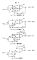
図1は上記オフセットキャンセル機能とスイッチフィードスルーオフセットキャンセル機能を有する、アナログバッファ20の回路構成図である。
【0026】
アナログバッファ20の入力端は、位相φ1,φ2で切替わる切替えスイッチ31に入力されている。スイッチ31の一端はクロックcl.1bでオンするスイッチ35,位相φ2でオンするスイッチ32,差動増幅器30の一方の入力端に接続され、スイッチ31の他端はクロックcl.2でオンするスイッチ36,クロックcl.1aでオンする切替えスイッチ34,位相φ1でオンするスイッチ33に接続されている。また差動増幅器30の他方の入力端は、cl.1aでオンする切替えスイッチ34とキャンセル容量37に接続され、キャンセル容量37の他端はクロックcl.1bでオンするスイッチ35とクロックcl.2でオンするスイッチ36に接続されている。そして差動増幅器30の出力端はアナログバッファ20の出力端に接続されると同時に、位相φ2でオンするスイッチ32と位相φ1でオンするスイッチ33に接続されている。なおここで差動増幅器30の図中に(A,B)で示した入力端子の符号は、表1に示すように位相φ1では(+,−)であり、位相φ2では(−,+)に切替わる。
【0027】
図2は上記の機能を有する差動増幅器30の回路構成図である。
【0028】
差動増幅器30は初段の差動回路と、次段のソースフォロア回路とから構成されている。差動回路は多結晶Si−ドライバTFT41,42と多結晶Si−負荷TFT43,44,所定のバイアスで駆動される多結晶Si−電流源TFT45とから成っており、その差動出力端は、位相φ1,φ2で切替わる多結晶Si−スイッチTFT群46,47,48,49によって切替えが可能である。これらのスイッチ群により、差動増幅器30のA,Bの入力の正負の切替えが行われる。多結晶Si−ドライバTFT51,所定のバイアスで駆動される多結晶Si−負荷TFT52で構成される次段のソースフォロア回路は、大出力電流の供給と動作点電圧の整合を図るために設けられている。なおここでVd1,Vs1,Vd2,Vs2はそれぞれ上記初段の差動回路の高,低電圧電源と上記次段のソースフォロア回路の高,低電圧電源である。
【0029】
以下に図4,図5を用いて本実施例の動作を詳細に説明する。
【0030】
始めに図4を用いて、本アナログバッファ20の動作を説明する。アナログバッファ20は位相φ1の前半において、スイッチ34m35を閉じて(a)オフセット量の記憶1を行う。このときキャンセル容量,Cm37の両端にはアナログバッファ20のオフセット電圧ΔVが入力されている。次いで位相φ1の後半においてはスイッチ36を閉じて(b)オフセット量の減算1を行う。このときアナログバッファ20のオフセット電圧ΔVを記憶したキャンセル容量,Cm37はアナログバッファ20の負帰還路に挿入されるため、差動増幅器30の出力電圧はΔVだけ小さくなる。これによってアナログバッファ20のオフセット電圧ΔVはキャンセルされるが、先に「発明が解決しようとする課題」の項でも述べたとおり、スイッチ34がオフになる際に差動増幅器30の負入力端側に生じたフィードスルー電荷q1に起因するスイッチフィードスルーオフセット電圧が、アナログバッファ20の出力端に(−q1/Cm)だけ生じてしまう。
【0031】
次にアナログバッファ20は位相φ2の前半において、スイッチ34,35を閉じて(c)オフセット量の記憶2を行う。このときもキャンセル容量Cm37の両端にはアナログバッファ20のオフセット電圧ΔVが入力される。次いで位相φ2の後半においてはスイッチ36を閉じて(d)オフセット量の減算2を行う。このときアナログバッファ20のオフセット電圧ΔVを記憶したキャンセル容量Cm37はアナログバッファ20の正入力端に挿入されるため、差動増幅器30の出力電圧はΔVだけ小さくなる。これによってアナログバッファ20のオフセット電圧ΔVはキャンセルされるが、このときにも先程と同様に、スイッチ34がオフになる際に差動増幅器30の正入力端側に生じたフィードスルー電荷q1に起因するスイッチフィードスルーオフセット電圧が、アナログバッファ20の出力端に(+q1/Cm)だけ生じる。しかしながら位相φ1とφ2でアナログバッファ20に入力する電圧が等しいと仮定すると、ここで生じるスイッチフィードスルーオフセット電圧は基本的に同一のTFTから同一の電圧条件で生じるものであるから両者のq1の値は等しいため、位相φ1とφ2でアナログバッファ20の出力端に生じるスイッチフィードスルーオフセット電圧は互いに正負が逆で値は等しくなることが判る。従って位相φ1とφ2をフレーム毎に交互に切替えることによって、上記スイッチフィードスルーオフセットを視覚的にキャンセルすることが可能であり、これによって問題であったスイッチフィードスルーオフセット電圧のばらつきも、同時に消去される。
【0032】
次に図5は本実施例における各動作パルスの、2フレーム(=4フィールド)期間内における同一の画素行書込み時のある列におけるタイミングチャートである。本実施例は奇遇2フレームを繰り返し単位として駆動される。本チャートにおいては、スイッチのオン/オフは、図中にも記したように上側をオン,下側をオフとして表わしてある。但し階調切替えスイッチ14,15のみ、選択されるアナログバッファ20A,20Bと階調選択スイッチ3A,3Bに対応させて、上をA,下をBとして示した。
【0033】
奇数フレーム期間・正フィールドの始めに位相φ1が選択され、階調切替えスイッチ14,15がA選択に切替わる。次いでゲート線駆動回路10によって選択された所定のゲート線13(画素TFT11)がオンし、アナログバッファ20Aのスイッチ36がオフする。続いてアナログバッファ20Aにおけるオフセットキャンセル回路の動作が開始される。一次ラッチ回路23の出力がオンすると共に、スイッチ34,35がオンしてキャンセル容量,Cm37の両端に差動増幅器30のオフセット電圧が入力する。次いでスイッチ34、そしてスイッチ35の順で両スイッチがオフするが、スイッチ35のフィードスルー電荷の影響を除去するためには、これらがオフする順序は大切である。先にスイッチ34がオフしてしまえば、この後に生じるスイッチ35のフィードスルー電荷はキャンセル容量,Cm37には入力されず、その影響を回避できるからである。次いでスイッチ36がオンすることによって、キャンセル容量,Cm37に記憶されていた差動増幅器30のオフセット電圧は負帰還路に入力され、多結晶Si−TFTを用いた差動増幅器30のTFT不整合に起因するオフセット電圧はキャンセルされる。この状態でアナログバッファ出力スイッチ16がオンすると、信号線7にはアナログバッファ20Aより画像信号電圧が出力される。この状態では差動増幅回路30の入力に接続されているスイッチ34のフィードスルー電荷のばらつきが、(−q1A/Cm)のスイッチフィードスルーオフセット電圧として信号線7を介して画素に入力されることは既に述べたとおりである。(ここではアナログバッファ20Aのスイッチ34のスイッチフィードスルー電荷をq1Aと記した。)この後ゲート線13(画素TFT11)、アナログバッファ出力スイッチ16がオフすることによって、選択された一行分の画素に対する書込み動作は終了する。アナログバッファ出力スイッチ16の役割は、必要に応じてアナログバッファ20A,20Bの出力を信号線7から切離すことによって、オフセットキャンセル動作時におけるアナログバッファ20A,20Bの出力の立ち上がりを高速化することである。
【0034】
次いで図示した奇数フレーム期間・負フィールドにおける、同一の画素行書込み時の動作を説明する。この動作は階調切替えスイッチ14,15がB選択に切替わることを除けば、上記奇数フレーム期間・正フィールドにおける書込み動作と基本的に同一である。本実施例においてはこのように正/負のフィールドで階調切替えスイッチ14,15を切替えることにより、液晶に対する交流駆動を実現している。本期間においても、差動増幅器30の入力に接続されているスイッチ34のフィードスルー電荷のばらつきが、(−q1B/Cm)のスイッチフィードスルーオフセット電圧として信号線7を介して画素に入力されることになる。(ここではアナログバッファ20Bのスイッチ34のスイッチフィードスルー電荷をq1Bと記した。)このときはアナログバッファは20Aに替えて20Bが用いられている訳であるから、このq1Bの値は、先のq1Aの値とは全く独立の値であることは明らかである。
【0035】
次に図示した偶数フレーム期間・正フィールドにおける、同一の画素行書込み時の動作を説明する。この動作は位相φ2が選択されることを除けば、上記奇数フレーム期間・正フィールドにおける書込み動作と同一である。前述のようにこの場合、差動増幅回路30の入力に接続されているスイッチ34のフィードスルー電荷のばらつきは、(+q1A/Cm)のスイッチフィードスルーオフセット電圧として信号線7を介して画素に入力される。ここで表示する画像データが奇数フレーム期間・正フィールドと偶数フレーム期間・正フィールドとで実質的に変化していなければ、両者のスイッチフィードスルーオフセット電圧は視覚的にキャンセルされ、筋状の輝度むらの発生は回避される。輝度むらが視覚的に問題となるのは、表示画像データの値が特に時間的に大きく変化しないときであるため、上記のオフセットキャンセル操作は実用的には十分な効果を有している。
【0036】
最後に図示した偶数フレーム期間・負フィールドにおける、同一の画素行書込み時の動作を説明する。この動作は位相φ2が選択されることを除けば、上記奇数フレーム期間・負フィールドにおける書込み動作と同一であり、このスイッチフィードスルーオフセット電圧の視覚的なキャンセル効果は上記と同様であるので、詳細な説明は省略する。
【0037】
上記実施例においては、各回路ブロックは多結晶Si−TFT素子を用いてガラス基板上に構成している。しかしながらガラス基板に変えて、石英基板,透明プラスチック基板を用いることや、液晶表示方式を反射型に変えることでSi基板を始めとする不透明基板を用いることも明らかに可能である。
【0038】
また上記差動増幅回路における、TFTのn型,p型の導電型を逆に構成することや、その他の回路構成を用いることも、本発明の原理を損なわない範囲で可能であることは言うまでもない。差動増幅器30の利得を向上させるために、カスコード構成を採用することもまた有効である。TFTには基板バイアス効果を持たないという長所があるものの、ドレインコンダクタンスが大きいという課題もあるため、バイアス端子が新たに必要にはなるものの、数百倍以上に差動増幅回路の利得を確保するためには、このようなカスコード構成の採用は有利である。
【0039】
以上では説明を簡略化するために画像表示データを6bit 、階調電源線は異なった階調電圧が印加された64本の並列配線としたが、画像表示データがn−bit であれば、階調電源線は異なった階調電圧が印加された2n本の並列配線となることは明らかである。
【0040】
この他、本実施例ではスイッチ群の構成はCMOSスイッチ、画素TFTはn型TFTスイッチを採用したが、p型TFTを含むいずれのスイッチ構成をこれらに用いても本発明の適用は可能である。また本発明の趣旨を逸脱しない範囲で、反射型表示画素構造等、多様な構造やレイアウト形状が適用可能であることは言うまでもない。
(第二の実施例)
第二の実施例である多結晶Si−TFT液晶表示パネルの全体構成は、第一の実施例のそれと同様であるので説明は省略する。第一の実施例と比較した場合の本実施例の差異は、各動作パルスの動作タイミングにある。以下、これに関して述べる。
【0041】
以下図6および図7を用いて、本発明における第二の実施例の動作に関して説明する。
【0042】
図6は本実施例における各動作パルスの、1フィールド期間における画素行書込み時のある列におけるタイミングチャートである。図6は第一の実施例における図5に対応するものであるが、ここではフィールドの正/負を切替える階調切替えスイッチ14,15に関しては記載を省略した。本実施例においては、階調切替えスイッチ14,15のA,Bの選択以外は、正および負フィールドにおける各パルスの動作は共通だからである。なお本チャートにおいても、スイッチのオン/オフは、図中にも記したように上側をオン,下側をオフとして表わしてある。
【0043】
1フィールドの始めに位相φ1が選択され、次いでゲート線駆動回路10によって選択された所定のゲート線13(画素TFT11)がオンし、スイッチ36がオフする。続いてアナログバッファ20(上記のようにアナログバッファ20A,20Bにおける動作は基本的に同一であるため、ここではアナログバッファ20として記載する)におけるオフセットキャンセル回路の動作が開始される。一次ラッチ回路23の出力がオンすると共に、スイッチ34,35がオンしてキャンセル容量,Cm37の両端に差動増幅器30のオフセット電圧が入力する。次いでスイッチ34、そしてスイッチ35の順で両スイッチがオフする。次いでスイッチ36がオンすることによって、キャンセル容量,Cm37に記憶されていた差動増幅器30のオフセット電圧は負帰還路に入力され、多結晶Si TFTを用いた差動増幅器30のTFT不整合に起因するオフセット電圧はキャンセルされる。この状態でアナログバッファ出力スイッチ16がオンすると、信号線7にはアナログバッファ20より画像信号電圧が出力される。この状態では差動増幅回路30の入力に接続されているスイッチ34のフィードスルー電荷のばらつきが、(−q1/Cm)のスイッチフィードスルーオフセット電圧として信号線7を介して画素に入力されることは第一の実施例と同様である。しかし本実施例においては、同一の画素行書込み時に連続して以下の動作が行われる。即ちアナログバッファ出力スイッチ16が一度オフした後に位相φ2が選択され、もう一度上記の画像信号電圧の出力動作が繰り返される。この場合には差動増幅回路30の入力に接続されているスイッチ34のフィードスルー電荷のばらつきが、(+q1/Cm)のスイッチフィードスルーオフセット電圧として信号線7を介して画素に入力されることになる。この後ゲート線13(画素TFT11),アナログバッファ出力スイッチ16がオフすることによって、選択された一行分の画素に対する書込み動作は終了する。
【0044】
図7は、上記の書込み動作によって信号線7に書込まれる画像信号電圧を示したものである。一回目にアナログバッファ出力スイッチ16がオンするt1からt2の期間には、信号線7には(Vin−q1/Cm)に漸近する出力信号が書込まれる。ただしここでVinは、本来信号線7に書込まれるべき画像信号電圧である。(図中ではq1は負の値を有しているものとして示している。)次いで二回目にアナログバッファ出力スイッチ16がオンするt3からt4の期間には、信号線7には(Vin+q1/Cm)に漸近する出力信号が書込まれる。ここで(t4−t3)の期間を(t2−t1)よりも小さい適当な値に設定することによって、最終的に信号線7に書込まれる画像信号電圧VAを、Vin近傍の値に近づけることができる。本実施例では上記手法を用いることによって、画素に入力されるスイッチフィードスルーオフセット電圧ばらつきの低減を実現している。
【0045】
なお本実施例においては1フィールド内における位相φ1/φ2の切替えを一回としたが、これをより多い回数行うことによっても同様な効果を得ることが可能である。
(第三の実施例)
第三の実施例である多結晶Si−TFT液晶表示パネルの全体構成は、第一の実施例のそれと同様であるので説明は省略する。第一の実施例と比較した場合の本実施例の差異は、アナログバッファ20A,20Bの回路構成とその動作パルスの動作タイミングにある。以下、これに関して述べる。
【0046】
図8はオフセットキャンセル機能とスイッチフィードスルーオフセットキャンセル機能を有する、本実施例におけるアナログバッファ20(なお本実施例においてもアナログバッファ20A,20Bにおける動作は基本的に同一であるため、ここでもアナログバッファ20として記載する)の回路構成図である。
【0047】
アナログバッファ20の入力端は、クロックcl.1bでオンするスイッチ55と、差動増幅器50の正入力端に接続され、また差動増幅器50の負入力端は、cl.1a1でオンするスイッチ54,cl.1a2でオンするスイッチ58とキャンセル容量57に接続され、キャンセル容量57の他端はクロックcl.1bでオンするスイッチ55とクロックcl.2でオンするスイッチ56に接続されている。そして差動増幅器50の出力端はアナログバッファの出力端に接続されると同時に、cl.1a1でオンするスイッチ54,cl.1a2でオンするスイッチ58,クロックcl.2でオンするスイッチ56の他端に接続されている。
【0048】
次に上記アナログバッファ20の動作に関して、図9を用いて説明する。
【0049】
図9は本実施例における各動作パルスの、1フィールド期間における画素行書込み時のある列におけるタイミングチャートであり、第二の実施例における図6に対応するものである。
【0050】
1フィールドの始めにゲート線駆動回路10によって選択された所定のゲート線13(画素TFT11)がオンし、スイッチ56がオフする。続いてアナログバッファにおけるオフセットキャンセル回路の動作が開始される。一次ラッチ回路23の出力がオンすると共に、スイッチ54,55,58がオンしてキャンセル容量,Cm57の両端に差動増幅器50のオフセット電圧が入力する。次いでスイッチ54,スイッチ58、そしてスイッチ55の順で各スイッチがオフする。次いでスイッチ56がオンすることによって、キャンセル容量,Cm57に記憶されていた差動増幅器50のオフセット電圧は負帰還路に入力され、多結晶Si−TFTを用いた差動増幅器50のTFT不整合に起因するオフセット電圧はキャンセルされる。この状態でアナログバッファ出力スイッチ16がオンすると、信号線7にはアナログバッファ20より画像信号電圧が出力される。ここで本実施例においては、後からオフするスイッチ58のゲート幅は、先にオフするスイッチ54のゲート幅よりも小さく設計されている。但し両者のゲート長は同一である。即ちキャンセル容量,Cm57への充電は、スイッチフィードスルー電荷量は大きいがオン抵抗のより低いスイッチ54を用いて行い、更にオン抵抗は大きいがスイッチフィードスルー電荷量のより小さいスイッチ58を用いてスイッチフィードスルー電荷量の低減を図っている。本実施例を用いれば、先の第一,第二の実施例よりも小さい回路規模で、スイッチフィードスルーオフセット電圧ばらつきの低減が可能である。
【0051】
なお本実施例では後からオフするスイッチ58のゲート幅を、先にオフするスイッチ54のゲート幅よりも小さく設計しているが、本発明の考え方は、後からオフするスイッチ58のゲートを先にオフするスイッチ54のゲートよりも低いゲート電圧で駆動する等、種々の応用も可能である。
(第四の実施例)
以下図10を用いて、本発明における第四の実施例に関して説明する。
【0052】
図10は第四の実施例である画像ビューア71の構成図である。
【0053】
無線インターフェース(I/F)回路73には、圧縮された画像データが外部からbluetooth 規格に基づく無線データとして入力し、無線I/F回路73の出力は中央演算ユニット(CPU)/デコーダ74を経てフレームメモリ75に接続される。更にCPU/デコーダ74の出力は多結晶Si液晶表示パネル76に設けられたインターフェース(I/F)回路77を介して行選択回路79およびデータ入力回路78に接続されており、画像表示領域80は行選択回路79およびデータ入力回路78により駆動される。画像ビューア71には更に電源82および光源81が設けられている。ここで多結晶Si液晶表示パネル76は、先に延べた第一の実施例と同一の構成および動作を有している。
【0054】
以下に本第四の実施例の動作を説明する。無線I/F回路73は圧縮された画像データを外部から取り込み、このデータをCPU/デコーダ74に転送する。CPU/デコーダ74はユーザからの操作を受けて、必要に応じて画像ビューア71を駆動、或いは圧縮された画像データのデコード処理を行う。デコードされた画像データはフレームメモリ75に一時的に蓄積され、CPU/デコーダ74の指示に従って、蓄積されていた画像を表示するための画像データおよびタイミングパルスをI/F回路77に出力する。I/F回路77が、これらの信号を用いて、行選択回路79およびデータ入力回路78を駆動して画像表示領域に画像を表示することに関しては、第一の実施例で述べたとおりであるので、ここでは詳細な説明は省略する。光源は液晶表示に対するバックライトであり、電源82には二次電池が含まれており、これらの装置全体を駆動する電源を供給する。
【0055】
本第四の実施例によれば、圧縮された画像データを元に、前述のように「スイッチフィードスルーオフセットばらつき」に起因する縦筋状の輝度むらのない、高品位な画像を表示させることができる。
【0056】
【発明の効果】
本発明によれば、高品位画像表示の可能な液晶画像表示装置を提供することができる。
【図面の簡単な説明】
【図1】第一の実施例におけるアナログバッファの回路構成図。
【図2】第一の実施例における差動増幅器の回路構成図。
【図3】第一の実施例における多結晶Si−TFT液晶表示パネルの構成図。
【図4】第一の実施例におけるアナログバッファの動作説明図。
【図5】第一の実施例におけるタイミングチャート。
【図6】第二の実施例におけるタイミングチャート。
【図7】第二の実施例におけるる信号線に書込まれる画像信号電圧説明図。
【図8】第三の実施例におけるアナログバッファの回路構成図。
【図9】第三の実施例におけるタイミングチャート。
【図10】第四の実施例である画像ビューアの構成図。
【図11】従来例であるTFT液晶パネル駆動用のオフセットキャンセルバッファ回路の構成図。
【符号の説明】
2A,2B…階調電源線、3A,3B…階調選択スイッチ、7…信号線、11…画素TFT、12…液晶容量、13…ゲート線、14,15…階調切替えスイッチ、16…アナログバッファ出力スイッチ、17…階調選択線、20A,20B…アナログバッファ、21…ラッチアドレス選択回路、22…デジタルデータ入力線、23…一次ラッチ回路、24…2次ラッチ回路、30…差動増幅回路、37…キャンセル容量、90…画像信号駆動回路、91…画像信号電圧発生部、92…出力インピーダンス変換手段。[0001]
BACKGROUND OF THE INVENTION
The present invention relates to a liquid crystal image display device capable of displaying a high quality image.
[0002]
[Prior art]
Hereinafter, a conventional technique will be described with reference to FIG.
[0003]
FIG. 11 is a configuration diagram of an offset cancel buffer circuit used in a low-temperature poly-Si driving circuit for driving a TFT liquid crystal panel using a conventional technique. The analog input signal Vin is buffered by a
[0004]
The operation of this conventional example will be described below. The positive and negative input parts of the
[0005]
The prior art is described in detail in, for example, the IEICE Technical Report EID98-125 (January 1999).
[0006]
Further, a peripheral circuit configuration when a similar offset cancel buffer circuit is configured by LSI and a TFT liquid crystal panel is driven is described in detail in, for example, Proceedings of Euro Display '96, pp.247-250.
[0007]
[Problems to be solved by the invention]
According to the above prior art, it is possible to cancel the offset voltage caused by the mismatch of the differential amplifier circuit. However, the switch 153 (FET (Field-Effect Transistor) switch) is the main cause of new output offset voltage variation, and it is invented that this must be taken to further improve the output voltage accuracy of the offset cancel circuit. They found out. This will be described below with reference to FIG.
[0008]
Here, for the purpose of explanation, the
[0009]
First, the
[0010]
[Expression 1]
ΔVout = −q1 · G / (G + 1)
Is required.
[0011]
Since the open gain G of the
[0012]
Since the role of the buffer circuit is impedance conversion, it is not preferable to design the input impedance to be small, and the
[0013]
In general, when a single crystal MOS transistor is used for the
[0014]
Here, the problem of the offset cancel circuit shown in FIG. 11 has been described as a problem caused by the
[0015]
From the above consideration, in the offset cancel buffer circuit using FET, the variation of the feedthrough charge, q1 of the offset canceling switch connected to the input of the differential amplifier circuit is a new “switch feedthrough offset variation”. In order to further improve the output voltage accuracy of the buffer circuit, it has become clear that new countermeasures are required.
[0016]
Note that the
[0017]
[Means for Solving the Problems]
The above problems include a liquid crystal counter electrode to which a predetermined voltage is applied, a pixel electrode provided to form a liquid crystal capacitor between the liquid crystal counter electrode, and a pixel switch connected in series to the pixel electrode. A plurality of display pixels arranged in a matrix for image display, image signal voltage generating means for outputting a first analog image signal voltage based on image data to be displayed, and a first analog image An output impedance conversion means group using a semiconductor element provided to output a second analog image signal voltage with an output impedance lower than that of the image signal voltage generation means, and an output impedance conversion means; The output offset of the second analog image signal voltage caused by variations in the semiconductor element characteristics in each output impedance conversion means group provided in the An offset canceling capacitor having one end connected to the voltage input terminal of the output impedance converting means and a first semiconductor switch having one end connected to the voltage input terminal of the output impedance converting means provided to cancel the variation Including an offset cancel circuit group, a signal line group connecting the output terminal of the output impedance conversion means group and the pixel switch group, and a second analog image signal voltage that is an output of the output impedance conversion means group as a signal line In the image display device having the signal voltage writing means for writing to the liquid crystal capacitance of the predetermined display pixel via the group and the pixel switch group, the switch feedthrough charge generated when the first semiconductor switch is turned off Means for reducing output variation of second analog image signal voltage caused by variation It can be solved by providing a new.
[0018]
DETAILED DESCRIPTION OF THE INVENTION
(First embodiment)
Hereinafter, the first embodiment of the present invention will be described with reference to FIGS. 1 to 5 and Table 1. FIG.
[0019]
FIG. 3 is a configuration diagram of a polycrystalline Si-TFT liquid crystal display panel according to this embodiment.
[0020]
Display pixels composed of a
[0021]
Since the image display data is 6 bits here, the gradation
[0022]
The outline of the operation of the present liquid crystal display panel will be described below. Details of the configuration and operation timing of the analog buffers 20A and 20B will be described later with reference to FIG. 1, Table 1, FIG. 2, FIG. The image display data input to the digital
[0023]
Next, the circuit configuration of the analog buffers 20A and 20B will be described with reference to FIGS. Here, since the analog buffers 20A and 20B have the same basic configuration, they are simply described as the analog buffer 20 below.
[0024]
[Table 1]
FIG. 1 is a circuit configuration diagram of an analog buffer 20 having the offset cancel function and the switch feedthrough offset cancel function.
[0026]
The input end of the analog buffer 20 is input to a
[0027]
FIG. 2 is a circuit configuration diagram of the
[0028]
The
[0029]
The operation of this embodiment will be described in detail below with reference to FIGS.
[0030]
First, the operation of the analog buffer 20 will be described with reference to FIG. In the first half of the phase φ1, the analog buffer 20 closes the switch 34m35 and (a) stores the offset
[0031]
Next, in the first half of the phase φ2, the analog buffer 20 closes the
[0032]
Next, FIG. 5 is a timing chart of a certain column at the time of writing the same pixel row within a period of 2 frames (= 4 fields) of each operation pulse in this embodiment. In the present embodiment, driving is performed by using 2 odd frames as a repeating unit. In this chart, the on / off state of the switch is represented by turning on the upper side and turning off the lower side as described in the figure. However, only the gradation changeover switches 14 and 15 are shown as A on the upper side and B on the lower side corresponding to the selected
[0033]
The phase φ1 is selected at the beginning of the odd frame period / positive field, and the gradation changeover switches 14 and 15 are switched to A selection. Next, a predetermined gate line 13 (pixel TFT 11) selected by the gate
[0034]
Next, an operation at the time of writing the same pixel row in the illustrated odd frame period / negative field will be described. This operation is basically the same as the writing operation in the odd frame period / positive field except that the gradation changeover switches 14 and 15 are switched to B selection. In this embodiment, the AC drive for the liquid crystal is realized by switching the gradation changeover switches 14 and 15 in the positive / negative field in this way. Even during this period, the variation in the feedthrough charge of the
[0035]
Next, an operation at the time of writing the same pixel row in the even-numbered frame period / positive field shown in the figure will be described. This operation is the same as the write operation in the odd frame period / positive field except that the phase φ2 is selected. As described above, in this case, the variation in the feedthrough charge of the
[0036]
Finally, the operation at the time of writing the same pixel row in the even-numbered frame period and negative field shown in the figure will be described. This operation is the same as the write operation in the odd frame period / negative field except that the phase φ2 is selected, and the visual canceling effect of the switch feedthrough offset voltage is the same as described above. Detailed explanation is omitted.
[0037]
In the above embodiment, each circuit block is formed on a glass substrate using a polycrystalline Si-TFT element. However, it is clearly possible to use a quartz substrate or a transparent plastic substrate instead of the glass substrate, or to use an opaque substrate such as a Si substrate by changing the liquid crystal display method to a reflective type.
[0038]
In addition, it is needless to say that the n-type and p-type conductivity types of the TFT in the differential amplifier circuit can be reversed and other circuit configurations can be used without departing from the principle of the present invention. Yes. In order to improve the gain of the
[0039]
In the above, for simplification of description, the image display data is 6 bits and the gradation power supply line is 64 parallel wirings to which different gradation voltages are applied. However, if the image display data is n-bit, the floor The dimming power supply line was applied with
[0040]
In addition, in this embodiment, the switch group configuration is a CMOS switch and the pixel TFT is an n-type TFT switch. However, the present invention can be applied to any switch configuration including a p-type TFT. . Needless to say, various structures and layout shapes such as a reflective display pixel structure can be applied without departing from the spirit of the present invention.
(Second embodiment)
Since the overall configuration of the polycrystalline Si-TFT liquid crystal display panel according to the second embodiment is the same as that of the first embodiment, the description thereof is omitted. The difference of this embodiment compared to the first embodiment is the operation timing of each operation pulse. This will be described below.
[0041]
The operation of the second embodiment of the present invention will be described below with reference to FIGS.
[0042]
FIG. 6 is a timing chart of a certain column at the time of pixel row writing in one field period of each operation pulse in this embodiment. FIG. 6 corresponds to FIG. 5 in the first embodiment, but the description of the gradation changeover switches 14 and 15 for switching the positive / negative of the field is omitted here. This is because, in this embodiment, the operations of the pulses in the positive and negative fields are common except for the selection of A and B of the gradation changeover switches 14 and 15. In this chart as well, the on / off state of the switch is represented with the upper side turned on and the lower side turned off as described in the figure.
[0043]
The phase φ1 is selected at the beginning of one field, then a predetermined gate line 13 (pixel TFT 11) selected by the gate
[0044]
FIG. 7 shows the image signal voltage written to the
[0045]
In this embodiment, the phase φ1 / φ2 is switched once in one field, but the same effect can be obtained by performing this switching more times.
(Third embodiment)
Since the overall structure of the polycrystalline Si-TFT liquid crystal display panel according to the third embodiment is the same as that of the first embodiment, the description thereof is omitted. The difference between this embodiment and the first embodiment is in the circuit configuration of the analog buffers 20A and 20B and the operation timing of the operation pulse. This will be described below.
[0046]
FIG. 8 shows an analog buffer 20 according to this embodiment having an offset cancel function and a switch feedthrough offset cancel function (note that the operations of the analog buffers 20A and 20B are basically the same in this embodiment as well. FIG. 20 is a circuit configuration diagram.
[0047]
The input terminal of the analog buffer 20 is connected to the clock cl. The
[0048]
Next, the operation of the analog buffer 20 will be described with reference to FIG.
[0049]
FIG. 9 is a timing chart of a certain column at the time of pixel row writing in one field period of each operation pulse in this embodiment, and corresponds to FIG. 6 in the second embodiment.
[0050]
A predetermined gate line 13 (pixel TFT 11) selected by the gate
[0051]
In this embodiment, the gate width of the
(Fourth embodiment)
Hereinafter, the fourth embodiment of the present invention will be described with reference to FIG.
[0052]
FIG. 10 is a block diagram of an
[0053]
Compressed image data is externally input to the wireless interface (I / F)
[0054]
The operation of the fourth embodiment will be described below. The wireless I /
[0055]
According to the fourth embodiment, based on the compressed image data, as described above, a high-quality image without vertical stripe-like luminance unevenness due to “switch feedthrough offset variation” is displayed. Can do.
[0056]
【The invention's effect】
ADVANTAGE OF THE INVENTION According to this invention, the liquid crystal image display apparatus in which a high quality image display is possible can be provided.
[Brief description of the drawings]
FIG. 1 is a circuit configuration diagram of an analog buffer according to a first embodiment.
FIG. 2 is a circuit configuration diagram of a differential amplifier in the first embodiment.
FIG. 3 is a configuration diagram of a polycrystalline Si-TFT liquid crystal display panel in the first embodiment.
FIG. 4 is an operation explanatory diagram of an analog buffer in the first embodiment.
FIG. 5 is a timing chart in the first embodiment.
FIG. 6 is a timing chart in the second embodiment.
FIG. 7 is an explanatory diagram of an image signal voltage written to a signal line in the second embodiment.
FIG. 8 is a circuit configuration diagram of an analog buffer according to a third embodiment.
FIG. 9 is a timing chart in the third embodiment.
FIG. 10 is a configuration diagram of an image viewer according to a fourth embodiment.
FIG. 11 is a configuration diagram of a conventional offset cancel buffer circuit for driving a TFT liquid crystal panel.
[Explanation of symbols]
2A, 2B ... gradation power supply line, 3A, 3B ... gradation selection switch, 7 ... signal line, 11 ... pixel TFT, 12 ... liquid crystal capacitor, 13 ... gate line, 14, 15 ... gradation switching switch, 16 ... analog Buffer output switch, 17 ... gradation selection line, 20A, 20B ... analog buffer, 21 ... latch address selection circuit, 22 ... digital data input line, 23 ... primary latch circuit, 24 ... secondary latch circuit, 30 ... differential
Claims (13)
表示すべき画像データに基づいて第一のアナログ画像信号電圧を出力する画像信号電圧発生手段と、
該第一のアナログ画像信号電圧を入力として、前記画像信号電圧発生手段より低い出力インピーダンスで、第二のアナログ画像信号電圧を出力するために設けられた半導体素子を用いた出力インピーダンス変換手段群と、
該出力インピーダンス変換手段群の中に設けられ、該各出力インピーダンス変換手段群における半導体素子特性のばらつきに起因する第二のアナログ画像信号電圧の出力オフセットばらつきをキャンセルするために設けられ、一端が該出力インピーダンス変換手段の電圧入力端子に接続されたオフセットキャンセル容量と、一端が該出力インピーダンス変換手段の電圧入力端子に接続された第一の半導体スイッチを有するオフセットキャンセル回路群と、
前記出力インピーダンス変換手段群の出力端子と、前記画素スイッチとを接続する信号線群と、
前記出力インピーダンス変換手段群の出力である第二のアナログ画像信号電圧を、前記信号線群と、前記画素スイッチ群を介して、所定の表示画素の液晶容量に書込むための信号電圧書込み手段と、
前記第一の半導体スイッチがオフする際に生成するスイッチフィードスルー電荷のばらつきに起因する、第二のアナログ画像信号電圧の出力ばらつきを低減する手段とを有し、
前記出力インピーダンス変換手段は差動増幅回路に負帰還をかけたボルテージフォロア回路を含む画像表示装置において、
前記オフセットキャンセル回路は、該差動増幅回路の第一の入力端子にその一端が接続された上記オフセットキャンセル容量と、該オフセットキャンセル容量の他端と該差動増幅回路の第二の入力端子を接続する第二の半導体スイッチと、該オフセットキャンセル容量の他端と第一のノードを接続する第三の半導体スイッチと、該差動増幅回路の第一の入力端子と第一のノードを接続する上記第一の半導体スイッチと、該差動増幅回路の第二の入力端子と該差動増幅回路の出力を接続する第四の半導体スイッチと、該第一のノードと該差動増幅回路の出力を接続する第五の半導体スイッチと、該オフセットキャンセル回路への入力を該差動増幅回路の第二の入力端子と該第一のノードのいずれかに選択的に接続させる第六の半導体スイッチと、該差動増幅回路の第一の入力端子を負入力にかつ第二の入力端子を正入力に設定することと該差動増幅回路の第一の入力端子を正入力にかつ第二の入力端子を負入力に設定することとを選択的に可能とする差動増幅回路正負反転手段を有する画像表示装置。A plurality of pixels each having a counter electrode to which a predetermined voltage is applied, a pixel electrode provided for forming a capacitance between the counter electrode, and a pixel switch connected in series to the pixel electrode Display section
Image signal voltage generating means for outputting a first analog image signal voltage based on image data to be displayed;
An output impedance conversion means group using a semiconductor element provided to output the second analog image signal voltage with an output impedance lower than that of the image signal voltage generation means, using the first analog image signal voltage as an input; and ,
Provided in the output impedance conversion means group, provided to cancel the output offset variation of the second analog image signal voltage caused by the variation in semiconductor element characteristics in each output impedance conversion means group, one end of the output impedance conversion means group An offset cancel capacitor connected to the voltage input terminal of the output impedance converter, and an offset cancel circuit group having a first semiconductor switch having one end connected to the voltage input terminal of the output impedance converter;
A signal line group connecting the output terminal of the output impedance conversion means group and the pixel switch;
A signal voltage writing means for writing a second analog image signal voltage, which is an output of the output impedance conversion means group, to the liquid crystal capacitance of a predetermined display pixel via the signal line group and the pixel switch group; ,
Means for reducing output variations of the second analog image signal voltage caused by variations in switch feedthrough charge generated when the first semiconductor switch is turned off;
In the image display device including the voltage follower circuit in which the output impedance conversion means applies negative feedback to the differential amplifier circuit.
The offset cancel circuit includes the offset cancel capacitor having one end connected to the first input terminal of the differential amplifier circuit, the other end of the offset cancel capacitor, and the second input terminal of the differential amplifier circuit. A second semiconductor switch to be connected, a third semiconductor switch to connect the other end of the offset cancellation capacitor and the first node, and a first input terminal of the differential amplifier circuit and the first node are connected. A first semiconductor switch; a fourth semiconductor switch for connecting a second input terminal of the differential amplifier circuit and an output of the differential amplifier circuit; an output of the first node and the differential amplifier circuit; A sixth semiconductor switch for selectively connecting the input to the offset cancel circuit to the second input terminal of the differential amplifier circuit and one of the first nodes; Setting the first input terminal of the differential amplifier circuit as a negative input and the second input terminal as a positive input; setting the first input terminal of the differential amplifier circuit as a positive input and a second input terminal An image display device having a differential amplifier circuit positive / negative inversion means that selectively enables a negative input to be set.
前記差動増幅回路正負反転手段は、該負荷FET対のゲートを該差動ドライバFET対のいずれかに選択的に接続する第七の半導体スイッチ対と、該第七の半導体スイッチ対の選択とは逆の差動ドライバFETから該差動増幅回路の出力を取る第八の半導体スイッチ対とを含む請求項1の画像表示装置。The differential amplifier circuit includes a current source, a differential driver FET pair, and a load FET pair whose gate is commonly connected to the drain of one of the differential driver FETs.
The differential amplifier circuit positive / negative inversion means includes a seventh semiconductor switch pair for selectively connecting a gate of the load FET pair to any one of the differential driver FET pairs, and a selection of the seventh semiconductor switch pair; The image display apparatus according to claim 1, further comprising: an eighth semiconductor switch pair that takes an output of the differential amplifier circuit from a reverse differential driver FET.
表示すべき画像データに基づいて第一のアナログ画像信号電圧を出力する画像信号電圧発生手段と、
該第一のアナログ画像信号電圧を入力として、該画像信号電圧発生手段より低い出力インピーダンスで、第二のアナログ画像信号電圧を出力するために設けられた、差動増幅回路に負帰還をかけたボルテージフォロア回路を含む出力インピーダンス変換手段群と、
該出力インピーダンス変換手段の中に設けられた、該各出力インピーダンス変換手段群における差動増幅回路を構成する半導体素子特性のばらつきに起因する第二のアナログ画像信号電圧の出力オフセットばらつきをキャンセルするために設けられた、該差動増幅回路の第一の入力端子にその一端が接続されたオフセットキャンセル容量と、該オフセットキャンセル容量の他端と該差動増幅回路の第二の入力端子を接続する第二の半導体スイッチと、該オフセットキャンセル容量の他端と第一のノードを接続する第三の半導体スイッチと、該差動増幅回路の第一の入力端子と第一のノードを接続する第一の半導体スイッチと、該差動増幅回路の第二の入力端子と該差動増幅回路の出力を接続する第四の半導体スイッチと、該第一のノードと該差動増幅回路の出力を接続する第五の半導体スイッチと、該オフセットキャンセル回路の入力を該差動増幅回路の第二の入力端子と該第一のノードのいずれかに選択的に接続させる第六の半導体スイッチと、該差動増幅回路の第一の入力端子を負入力にかつ第二の入力端子を正入力に設定することと該差動増幅回路の第一の入力端子を正入力にかつ第二の入力端子を負入力に設定することとを選択的に可能とする差動増幅回路正負反転手段を有するオフセットキャンセル回路群と、
該出力インピーダンス変換手段群の出力端子と該画素スイッチ群とを接続する信号線群と、
該出力インピーダンス変換手段群の出力である第二のアナログ画像信号電圧を、該信号線群と該画素スイッチ群を介して、所定の表示画素の液晶容量に書込むための信号電圧書込み手段とを有する画像表示装置において、
該第四の半導体スイッチをオフ,該第五の半導体スイッチをオン、該第六の半導体スイッチを該差動増幅回路の第二の入力端子に接続した状態で、該第一,第二,第三の半導体スイッチを所定の順序で開閉してオフセットキャンセルを行う第一のオフセットキャンセル動作と、該第四の半導体スイッチをオン,該第五の半導体スイッチをオフ、該第六の半導体スイッチを該第一のノードに接続した状態で、該第一,第二,第三の半導体スイッチを所定の順序で開閉してオフセットキャンセルを行う第二のオフセットキャンセル動作とを選択的に行うことを特徴とする画像表示装置の駆動方法。A plurality of pixels each having a counter electrode to which a predetermined voltage is applied, a pixel electrode provided for forming a capacitance between the counter electrode, and a pixel switch connected in series to the pixel electrode Display section
Image signal voltage generating means for outputting a first analog image signal voltage based on image data to be displayed;
Using the first analog image signal voltage as an input, negative feedback is applied to the differential amplifier circuit provided to output the second analog image signal voltage with lower output impedance than the image signal voltage generating means. A group of output impedance conversion means including a voltage follower circuit;
In order to cancel the output offset variation of the second analog image signal voltage caused by the variation in the characteristics of the semiconductor elements constituting the differential amplifier circuit in each output impedance conversion unit group provided in the output impedance conversion unit An offset cancel capacitor having one end connected to the first input terminal of the differential amplifier circuit, and the other end of the offset cancel capacitor connected to the second input terminal of the differential amplifier circuit. A second semiconductor switch, a third semiconductor switch connecting the other end of the offset cancel capacitor and the first node, and a first input connecting the first input terminal of the differential amplifier circuit and the first node. A semiconductor switch, a fourth semiconductor switch connecting the second input terminal of the differential amplifier circuit and the output of the differential amplifier circuit, the first node, and the A fifth semiconductor switch for connecting the output of the dynamic amplifier circuit; and a sixth semiconductor switch for selectively connecting the input of the offset cancel circuit to either the second input terminal of the differential amplifier circuit or the first node A first input terminal of the differential amplifier circuit as a negative input and a second input terminal as a positive input; and the first input terminal of the differential amplifier circuit as a positive input; An offset cancel circuit group having a differential amplifier circuit positive / negative inversion means that selectively enables the second input terminal to be set to a negative input;
A signal line group connecting the output terminal of the output impedance conversion means group and the pixel switch group;
Signal voltage writing means for writing the second analog image signal voltage, which is the output of the output impedance conversion means group, to the liquid crystal capacitance of a predetermined display pixel via the signal line group and the pixel switch group. In an image display apparatus having
With the fourth semiconductor switch off, the fifth semiconductor switch on, and the sixth semiconductor switch connected to the second input terminal of the differential amplifier circuit, the first, second, second A first offset cancel operation in which the three semiconductor switches are opened and closed in a predetermined order to cancel the offset, the fourth semiconductor switch is turned on, the fifth semiconductor switch is turned off, and the sixth semiconductor switch is turned on A second offset canceling operation for selectively performing offset cancellation by opening and closing the first, second, and third semiconductor switches in a predetermined order in a state of being connected to the first node, Method for driving an image display device.
表示すべき画像データに基づいて第一のアナログ画像信号電圧を出力する画像信号電圧発生手段と、
該第一のアナログ画像信号電圧を入力として、該画像信号電圧発生手段より低い出力インピーダンスで、第二のアナログ画像信号電圧を出力するために設けられた、差動増幅回路に負帰還をかけたボルテージフォロア回路を含む出力インピーダンス変換手段群と、
該出力インピーダンス変換手段の中には、該各出力インピーダンス変換手段群における差動増幅回路を構成する半導体素子特性のばらつきに起因する第二のアナログ画像信号電圧の出力オフセットばらつきをキャンセルするために設けられた、該差動増幅回路の負入力端子にその一端が接続された上記オフセットキャンセル容量と、該オフセットキャンセル容量の他端と該差動増幅回路の正入力端子を接続する第二の半導体スイッチと、該オフセットキャンセル容量の他端と該差動増幅回路の出力端とを接続する第三の半導体スイッチと、該差動増幅回路の負入力端子と該差動増幅回路の出力端を接続する第一の半導体スイッチとを有し、更に該オフセットキャンセル回路の入力が該差動増幅回路の正入力端子に接続され、該第一の半導体スイッチが複数の半導体スイッチの並列接続で構成されているオフセットキャンセル回路群と、
該出力インピーダンス変換手段群の出力端子と該画素スイッチ群とを接続する信号線群と、
該出力インピーダンス変換手段群の出力である第二のアナログ画像信号電圧を、該信号線群と該画素スイッチ群を介して、所定の表示画素の液晶容量に書込むための信号電圧書込み手段とを有する画像表示装置において、
該第一,第二,第三の半導体スイッチを所定の順序で開閉してオフセットキャンセル動作を行う際に、該第一の半導体スイッチを構成する複数の半導体スイッチを時系列的に順次オフすることを特徴とする画像表示装置の駆動方法。A plurality of pixels each having a counter electrode to which a predetermined voltage is applied, a pixel electrode provided for forming a capacitance between the counter electrode, and a pixel switch connected in series to the pixel electrode Display section
Image signal voltage generating means for outputting a first analog image signal voltage based on image data to be displayed;
Using the first analog image signal voltage as an input, negative feedback is applied to the differential amplifier circuit provided to output the second analog image signal voltage with lower output impedance than the image signal voltage generating means. A group of output impedance conversion means including a voltage follower circuit;
The output impedance conversion means is provided in order to cancel the output offset variation of the second analog image signal voltage caused by the variation in characteristics of the semiconductor elements constituting the differential amplifier circuit in each output impedance conversion means group. The offset cancel capacitor having one end connected to the negative input terminal of the differential amplifier circuit, and a second semiconductor switch connecting the other end of the offset cancel capacitor and the positive input terminal of the differential amplifier circuit A third semiconductor switch that connects the other end of the offset cancellation capacitor and the output terminal of the differential amplifier circuit, and a negative input terminal of the differential amplifier circuit and an output terminal of the differential amplifier circuit. that the first and a semiconductor switch, further inputs the offset cancel circuit is connected to the positive input terminal of the differential amplifier circuit, said first semiconductor scan An offset cancel circuit group which pitch is constituted by parallel connection of a plurality of semiconductor switches,
A signal line group connecting the output terminal of the output impedance conversion means group and the pixel switch group;
Signal voltage writing means for writing the second analog image signal voltage, which is the output of the output impedance conversion means group, to the liquid crystal capacitance of a predetermined display pixel via the signal line group and the pixel switch group. In an image display apparatus having
When the offset cancel operation is performed by opening and closing the first, second, and third semiconductor switches in a predetermined order, the plurality of semiconductor switches constituting the first semiconductor switch are sequentially turned off in time series. A driving method of an image display device characterized by the above.
前記一対の基板の少なくともいずれか一方の基板に、複数の走査線と、該複数の走査線に交差するように配置した複数の信号線とを有して表示部を構成し、
前記走査線に接続された走査信号駆動回路と、
前記信号線に接続され、表示すべき画像データに基づいて第1のアナログ画像信号電圧を生成する画像信号駆動回路を有し、
前記画像信号駆動回路は、前記第1のアナログ画像信号電圧を前記表示部に送信する際に、該第1のアナログ画像信号電圧を、該第1のアナログ画像信号電圧より低いインピーダンスの第2のアナログ画像信号電圧に変換する出力インピーダンス変換手段を有し、
該出力インピーダンス変換手段は、内部にスイッチング素子として用いられる複数の半導体素子と、差動増幅回路を有し、
前記差動増幅器は第1の入力端及び第2の入力端を有し、
前記複数の半導体素子によって、
前記第1のタイミングでは、前記出力インピーダンス変換手段の入力と前記差動増幅回路の前記第1の入力端とオフセットキャンセル容量の一端が接続され、前記オフセットキャンセル容量の他端と前記差動増幅回路の前記第2の入力端と前記差動増幅回路の出力端が接続され、
前記第2のタイミングでは、前記出力インピーダンス変換手段の入力と前記差動増幅回路の前記第1の入力端が接続され、前記オフセットキャンセル容量の一端と前記差動増幅回路の出力端が接続され、前記オフセットキャンセル容量の他端と前記差動増幅回路の前記第2の入力端が接続され、
前記第3のタイミングでは、前記出力インピーダンス変換手段の入力と前記オフセットキャンセル容量の他端と前記差動増幅回路の前記第2の入力端が接続され、前記オフセットキャンセル容量の一端と前記差動増幅回路の前記第1の入力端と前記差動増幅回路の出力端が接続され、
前記第4のタイミングでは、前記出力インピーダンス変換手段の入力と前記オフセットキャンセル容量の一端が接続され、前記オフセットキャンセル容量の他端と前記差動増幅回路の前記第2の入力端が接続され、前記差動増幅回路の前記第1の入力端と前記差動増幅回路の出力端が接続されることを特徴とする液晶表示装置。A pair of substrates, at least one of which is transparent, and a liquid crystal layer disposed between the pair of substrates,
On at least one of the pair of substrates, the display unit includes a plurality of scanning lines and a plurality of signal lines arranged to intersect the plurality of scanning lines,
A scanning signal driving circuit connected to the scanning line;
Connected to the signal line, to have a picture signal driving circuit for generating a first analog image signal voltage based on the image data to be displayed,
When the image signal driving circuit transmits the first analog image signal voltage to the display unit, the image signal driving circuit converts the first analog image signal voltage to a second impedance having a lower impedance than the first analog image signal voltage. Having an output impedance converting means for converting to an analog image signal voltage;
Output impedance conversion means, possess a plurality of semiconductor elements used as switching elements therein, a differential amplifier circuit,
The differential amplifier has a first input end and a second input end;
By the plurality of semiconductor elements,
At the first timing, an input of the output impedance converting means, the first input terminal of the differential amplifier circuit, and one end of an offset cancel capacitor are connected, and the other end of the offset cancel capacitor and the differential amplifier circuit And the second input terminal of the differential amplification circuit is connected to the output terminal of the differential amplifier circuit,
In the second timing, the input of the output impedance converting means and the first input terminal of the differential amplifier circuit are connected, and one end of the offset cancellation capacitor and the output terminal of the differential amplifier circuit are connected, The other end of the offset cancellation capacitor and the second input end of the differential amplifier circuit are connected,
At the third timing, the input of the output impedance converter, the other end of the offset cancel capacitor, and the second input end of the differential amplifier circuit are connected, and one end of the offset cancel capacitor and the differential amplifier are connected. The first input terminal of the circuit and the output terminal of the differential amplifier circuit are connected;
In the fourth timing, the input of the output impedance conversion means and one end of the offset cancel capacitor are connected, the other end of the offset cancel capacitor and the second input end of the differential amplifier circuit are connected, A liquid crystal display device , wherein the first input terminal of a differential amplifier circuit and the output terminal of the differential amplifier circuit are connected .
Priority Applications (5)
| Application Number | Priority Date | Filing Date | Title |
|---|---|---|---|
| JP2000226188A JP4449189B2 (en) | 2000-07-21 | 2000-07-21 | Image display device and driving method thereof |
| EP01114025.8A EP1174852B1 (en) | 2000-07-21 | 2001-06-08 | Picture image display device and method of driving the same |
| TW090114336A TW578134B (en) | 2000-07-21 | 2001-06-13 | Picture image display device and method of driving the same |
| US09/881,719 US6784865B2 (en) | 2000-07-21 | 2001-06-18 | Picture image display device with improved switch feed through offset cancel circuit and method of driving the same |
| KR1020010044041A KR100758086B1 (en) | 2000-07-21 | 2001-07-21 | Picture image display device and method of driving the same |
Applications Claiming Priority (1)
| Application Number | Priority Date | Filing Date | Title |
|---|---|---|---|
| JP2000226188A JP4449189B2 (en) | 2000-07-21 | 2000-07-21 | Image display device and driving method thereof |
Publications (3)
| Publication Number | Publication Date |
|---|---|
| JP2002041001A JP2002041001A (en) | 2002-02-08 |
| JP2002041001A5 JP2002041001A5 (en) | 2006-03-23 |
| JP4449189B2 true JP4449189B2 (en) | 2010-04-14 |
Family
ID=18719847
Family Applications (1)
| Application Number | Title | Priority Date | Filing Date |
|---|---|---|---|
| JP2000226188A Expired - Fee Related JP4449189B2 (en) | 2000-07-21 | 2000-07-21 | Image display device and driving method thereof |
Country Status (5)
| Country | Link |
|---|---|
| US (1) | US6784865B2 (en) |
| EP (1) | EP1174852B1 (en) |
| JP (1) | JP4449189B2 (en) |
| KR (1) | KR100758086B1 (en) |
| TW (1) | TW578134B (en) |
Families Citing this family (43)
| Publication number | Priority date | Publication date | Assignee | Title |
|---|---|---|---|---|
| WO2001009672A1 (en) * | 1999-07-30 | 2001-02-08 | Hitachi, Ltd. | Image display device |
| JP2003283271A (en) | 2002-01-17 | 2003-10-03 | Semiconductor Energy Lab Co Ltd | Electric circuit |
| DE10303427A1 (en) * | 2002-02-06 | 2003-10-16 | Nec Corp Tokio Tokyo | Amplifier circuit, driver circuit for a display device, portable telephone and portable electronic device |
| JP4168668B2 (en) | 2002-05-31 | 2008-10-22 | ソニー株式会社 | Analog buffer circuit, display device and portable terminal |
| US7193593B2 (en) * | 2002-09-02 | 2007-03-20 | Semiconductor Energy Laboratory Co., Ltd. | Liquid crystal display device and method of driving a liquid crystal display device |
| JP2004094058A (en) | 2002-09-02 | 2004-03-25 | Semiconductor Energy Lab Co Ltd | Liquid crystal display and its driving method |
| CN1589461A (en) * | 2002-10-11 | 2005-03-02 | 三菱电机株式会社 | Display device |
| US6911964B2 (en) * | 2002-11-07 | 2005-06-28 | Duke University | Frame buffer pixel circuit for liquid crystal display |
| US6958651B2 (en) | 2002-12-03 | 2005-10-25 | Semiconductor Energy Laboratory Co., Ltd. | Analog circuit and display device using the same |
| KR100510500B1 (en) * | 2002-12-05 | 2005-08-26 | 삼성전자주식회사 | TFT-LCD source driver integrated circuit for improving display quality and Method for eliminating offset of output amplifier |
| WO2004109638A1 (en) * | 2003-06-06 | 2004-12-16 | Semiconductor Energy Laboratory Co., Ltd. | Semiconductor device |
| JP4662698B2 (en) * | 2003-06-25 | 2011-03-30 | ルネサスエレクトロニクス株式会社 | Current source circuit and current setting method |
| KR100557501B1 (en) * | 2003-06-30 | 2006-03-07 | 엘지.필립스 엘시디 주식회사 | Analog buffer and method for driving the same |
| KR100649245B1 (en) * | 2003-11-29 | 2006-11-24 | 삼성에스디아이 주식회사 | Demultiplexer, and display apparatus using the same |
| KR100973819B1 (en) | 2003-12-04 | 2010-08-03 | 삼성전자주식회사 | Analog amplifier for flat panel display |
| JP4263153B2 (en) * | 2004-01-30 | 2009-05-13 | Necエレクトロニクス株式会社 | Display device, drive circuit for display device, and semiconductor device for drive circuit |
| JP2005266365A (en) * | 2004-03-18 | 2005-09-29 | Semiconductor Energy Lab Co Ltd | Source follower circuit, driving method thereof, voltage follower circuit, and display apparatus |
| JP2005331900A (en) * | 2004-06-30 | 2005-12-02 | Eastman Kodak Co | Display apparatus |
| JP4371006B2 (en) * | 2004-08-17 | 2009-11-25 | セイコーエプソン株式会社 | Source driver and electro-optical device |
| JP2006099850A (en) * | 2004-09-29 | 2006-04-13 | Nec Electronics Corp | Sample-and-hold circuit, drive circuit and display device |
| JP4503445B2 (en) * | 2005-01-12 | 2010-07-14 | シャープ株式会社 | Buffer circuit with voltage level amplification function and liquid crystal display device |
| JP4798753B2 (en) * | 2005-02-28 | 2011-10-19 | ルネサスエレクトロニクス株式会社 | Display control circuit and display control method |
| JP2006285018A (en) | 2005-04-01 | 2006-10-19 | Matsushita Electric Ind Co Ltd | Liquid crystal driving device, liquid crystal display apparatus and method for driving liquid crystal |
| KR100697287B1 (en) * | 2005-07-14 | 2007-03-20 | 삼성전자주식회사 | Source driver and driving method thereof |
| JP4736618B2 (en) | 2005-08-16 | 2011-07-27 | ソニー株式会社 | Amplifier circuit and display device |
| JP2007101630A (en) * | 2005-09-30 | 2007-04-19 | Matsushita Electric Ind Co Ltd | Voltage driving device |
| TWI449009B (en) * | 2005-12-02 | 2014-08-11 | Semiconductor Energy Lab | Display device and electronic device using the same |
| JP2007279186A (en) * | 2006-04-04 | 2007-10-25 | Nec Electronics Corp | Amplifier circuit and driving circuit |
| TW200743085A (en) * | 2006-05-05 | 2007-11-16 | Denmos Technology Inc | Cancelable offset driver apparatus and cancelable offset amplifier apparatus thereof |
| JP4890955B2 (en) * | 2006-06-14 | 2012-03-07 | オリンパス株式会社 | Solid-state imaging device |
| KR100807504B1 (en) * | 2006-12-06 | 2008-02-26 | 동부일렉트로닉스 주식회사 | Method for removing offset of analog buffer |
| JP4512647B2 (en) | 2008-03-03 | 2010-07-28 | Okiセミコンダクタ株式会社 | Driving device for image display device |
| JP5172434B2 (en) * | 2008-04-01 | 2013-03-27 | ラピスセミコンダクタ株式会社 | Display drive device and drive circuit layout method |
| CN101847378B (en) * | 2009-03-27 | 2012-07-04 | 北京京东方光电科技有限公司 | Source driving chip |
| US20110050665A1 (en) * | 2009-08-28 | 2011-03-03 | Himax Technologies Limited | Source driver and compensation method for offset voltage of output buffer thereof |
| JP2012256012A (en) | 2010-09-15 | 2012-12-27 | Semiconductor Energy Lab Co Ltd | Display device |
| TWI437532B (en) * | 2011-07-01 | 2014-05-11 | Novatek Microelectronics Corp | Gate driver and display apparatus using the same |
| US8810311B2 (en) * | 2012-03-14 | 2014-08-19 | Texas Instruments Incorporated | Auto-zeroed amplifier with low input leakage |
| JP2014171114A (en) * | 2013-03-04 | 2014-09-18 | Sony Corp | Level conversion circuit, multivalued output differential amplifier and display device |
| KR102044557B1 (en) | 2013-04-19 | 2019-11-14 | 매그나칩 반도체 유한회사 | A column driver for a graphics display |
| KR20140145429A (en) * | 2013-06-13 | 2014-12-23 | 삼성디스플레이 주식회사 | Display device |
| JPWO2016038855A1 (en) | 2014-09-12 | 2017-05-25 | 株式会社Joled | Source driver circuit and display device |
| US10796665B1 (en) * | 2019-05-07 | 2020-10-06 | Novatek Microelectronics Corp. | Control apparatus for driving display panel and method thereof |
Family Cites Families (16)
| Publication number | Priority date | Publication date | Assignee | Title |
|---|---|---|---|---|
| DE3304814C2 (en) * | 1983-02-11 | 1985-06-27 | SGS-ATES Deutschland Halbleiter-Bauelemente GmbH, 8018 Grafing | Differential amplifier |
| JPS59154808A (en) * | 1983-02-23 | 1984-09-03 | Hitachi Ltd | Amplifier circuit and semiconductor integrated circuit using it |
| DE69020036T2 (en) * | 1989-04-04 | 1996-02-15 | Sharp Kk | Control circuit for a matrix display device with liquid crystals. |
| JPH0456888A (en) * | 1990-06-25 | 1992-02-24 | Nippon Telegr & Teleph Corp <Ntt> | Dot matrix driving circuit |
| JP2743683B2 (en) * | 1991-04-26 | 1998-04-22 | 松下電器産業株式会社 | Liquid crystal drive |
| US5734366A (en) * | 1993-12-09 | 1998-03-31 | Sharp Kabushiki Kaisha | Signal amplifier, signal amplifier circuit, signal line drive circuit and image display device |
| JP3352876B2 (en) * | 1996-03-11 | 2002-12-03 | 株式会社東芝 | Output circuit and liquid crystal display driving circuit including the same |
| GB2312773A (en) * | 1996-05-01 | 1997-11-05 | Sharp Kk | Active matrix display |
| JP4095174B2 (en) * | 1997-08-05 | 2008-06-04 | 株式会社東芝 | Liquid crystal display device |
| JP3595153B2 (en) * | 1998-03-03 | 2004-12-02 | 株式会社 日立ディスプレイズ | Liquid crystal display device and video signal line driving means |
| JPH11305735A (en) * | 1998-04-17 | 1999-11-05 | Sharp Corp | Differential amplifier circuit, operational amplifier circuit using same, and liquid crystal driving circuit using the operational amplifier circuit |
| JP3998343B2 (en) * | 1998-10-05 | 2007-10-24 | 三菱電機株式会社 | Offset voltage compensation circuit |
| JP4510955B2 (en) * | 1999-08-30 | 2010-07-28 | 日本テキサス・インスツルメンツ株式会社 | Data line drive circuit for liquid crystal display |
| JP2001125543A (en) * | 1999-10-27 | 2001-05-11 | Nec Corp | Liquid crystal driving circuit |
| JP3993725B2 (en) * | 1999-12-16 | 2007-10-17 | 松下電器産業株式会社 | Liquid crystal drive circuit, semiconductor integrated circuit, and liquid crystal panel |
| JP3420148B2 (en) * | 1999-12-20 | 2003-06-23 | 山形日本電気株式会社 | Liquid crystal driving method and liquid crystal driving circuit |
-
2000
- 2000-07-21 JP JP2000226188A patent/JP4449189B2/en not_active Expired - Fee Related
-
2001
- 2001-06-08 EP EP01114025.8A patent/EP1174852B1/en not_active Expired - Lifetime
- 2001-06-13 TW TW090114336A patent/TW578134B/en not_active IP Right Cessation
- 2001-06-18 US US09/881,719 patent/US6784865B2/en not_active Expired - Lifetime
- 2001-07-21 KR KR1020010044041A patent/KR100758086B1/en active IP Right Grant
Also Published As
| Publication number | Publication date |
|---|---|
| JP2002041001A (en) | 2002-02-08 |
| KR100758086B1 (en) | 2007-09-11 |
| EP1174852A3 (en) | 2002-08-28 |
| US6784865B2 (en) | 2004-08-31 |
| TW578134B (en) | 2004-03-01 |
| EP1174852B1 (en) | 2015-01-14 |
| KR20020013713A (en) | 2002-02-21 |
| EP1174852A2 (en) | 2002-01-23 |
| US20020033786A1 (en) | 2002-03-21 |
Similar Documents
| Publication | Publication Date | Title |
|---|---|---|
| JP4449189B2 (en) | Image display device and driving method thereof | |
| JP4089227B2 (en) | Image display device | |
| JP6441516B2 (en) | Semiconductor device | |
| US7079127B2 (en) | Reference voltage generation circuit, display driver circuit, display device, and method of generating reference voltage | |
| US7071669B2 (en) | Reference voltage generation circuit, display driver circuit, display device, and method of generating reference voltage | |
| JP4847702B2 (en) | Display device drive circuit | |
| US7405720B2 (en) | Analog buffer circuit, display device and portable terminal | |
| JP3520418B2 (en) | Operational amplifier circuit, drive circuit, and control method of operational amplifier circuit | |
| JPH10153986A (en) | Display device | |
| JP3930992B2 (en) | Drive circuit for liquid crystal display panel and liquid crystal display device | |
| JP2011008028A (en) | Signal line driving circuit, display device, and electronic equipment | |
| US7545355B2 (en) | Image display apparatus and driving method thereof | |
| TW554208B (en) | Image display apparatus and driving method thereof | |
| KR20070002412A (en) | Analog sampling apparatus for liquid crystal display | |
| JP4161484B2 (en) | Electro-optical device drive circuit, electro-optical device, and electronic apparatus | |
| JP2008112143A (en) | Source-follower type analogue buffer, compensating operation method thereof, and display using the same | |
| US7696911B2 (en) | Amplifier circuit, digital-to-analog conversion circuit, and display device | |
| JP4145988B2 (en) | Analog buffer and display device | |
| JPH09223948A (en) | Shift register circuit and image display device | |
| JP4606577B2 (en) | Liquid crystal display device | |
| KR20040110621A (en) | drive IC of Liquid Crystal Display | |
| KR101177570B1 (en) | Data Output Buffer of Liquid Crystal Display | |
| JP4962402B2 (en) | Electro-optical device drive circuit, electro-optical device, and electronic apparatus | |
| JPH0730395A (en) | Logic circuit |
Legal Events
| Date | Code | Title | Description |
|---|---|---|---|
| A521 | Written amendment |
Free format text: JAPANESE INTERMEDIATE CODE: A523 Effective date: 20060202 |
|
| A621 | Written request for application examination |
Free format text: JAPANESE INTERMEDIATE CODE: A621 Effective date: 20060202 |
|
| RD01 | Notification of change of attorney |
Free format text: JAPANESE INTERMEDIATE CODE: A7421 Effective date: 20060418 |
|
| A977 | Report on retrieval |
Free format text: JAPANESE INTERMEDIATE CODE: A971007 Effective date: 20090324 |
|
| A131 | Notification of reasons for refusal |
Free format text: JAPANESE INTERMEDIATE CODE: A131 Effective date: 20091006 |
|
| A521 | Written amendment |
Free format text: JAPANESE INTERMEDIATE CODE: A523 Effective date: 20091202 |
|
| TRDD | Decision of grant or rejection written | ||
| A01 | Written decision to grant a patent or to grant a registration (utility model) |
Free format text: JAPANESE INTERMEDIATE CODE: A01 Effective date: 20100105 |
|
| A01 | Written decision to grant a patent or to grant a registration (utility model) |
Free format text: JAPANESE INTERMEDIATE CODE: A01 |
|
| A61 | First payment of annual fees (during grant procedure) |
Free format text: JAPANESE INTERMEDIATE CODE: A61 Effective date: 20100118 |
|
| R151 | Written notification of patent or utility model registration |
Ref document number: 4449189 Country of ref document: JP Free format text: JAPANESE INTERMEDIATE CODE: R151 |
|
| FPAY | Renewal fee payment (event date is renewal date of database) |
Free format text: PAYMENT UNTIL: 20130205 Year of fee payment: 3 |
|
| FPAY | Renewal fee payment (event date is renewal date of database) |
Free format text: PAYMENT UNTIL: 20130205 Year of fee payment: 3 |
|
| S111 | Request for change of ownership or part of ownership |
Free format text: JAPANESE INTERMEDIATE CODE: R313113 |
|
| FPAY | Renewal fee payment (event date is renewal date of database) |
Free format text: PAYMENT UNTIL: 20130205 Year of fee payment: 3 |
|
| R350 | Written notification of registration of transfer |
Free format text: JAPANESE INTERMEDIATE CODE: R350 |
|
| S111 | Request for change of ownership or part of ownership |
Free format text: JAPANESE INTERMEDIATE CODE: R313121 Free format text: JAPANESE INTERMEDIATE CODE: R313115 |
|
| FPAY | Renewal fee payment (event date is renewal date of database) |
Free format text: PAYMENT UNTIL: 20130205 Year of fee payment: 3 |
|
| R350 | Written notification of registration of transfer |
Free format text: JAPANESE INTERMEDIATE CODE: R350 |
|
| FPAY | Renewal fee payment (event date is renewal date of database) |
Free format text: PAYMENT UNTIL: 20140205 Year of fee payment: 4 |
|
| R250 | Receipt of annual fees |
Free format text: JAPANESE INTERMEDIATE CODE: R250 |
|
| R250 | Receipt of annual fees |
Free format text: JAPANESE INTERMEDIATE CODE: R250 |
|
| R250 | Receipt of annual fees |
Free format text: JAPANESE INTERMEDIATE CODE: R250 |
|
| R250 | Receipt of annual fees |
Free format text: JAPANESE INTERMEDIATE CODE: R250 |
|
| R250 | Receipt of annual fees |
Free format text: JAPANESE INTERMEDIATE CODE: R250 |
|
| R250 | Receipt of annual fees |
Free format text: JAPANESE INTERMEDIATE CODE: R250 |
|
| LAPS | Cancellation because of no payment of annual fees |