CN100435286C - Method of forming a nanocluster charge storage device - Google Patents
Method of forming a nanocluster charge storage device Download PDFInfo
- Publication number
- CN100435286C CN100435286C CNB2005800210850A CN200580021085A CN100435286C CN 100435286 C CN100435286 C CN 100435286C CN B2005800210850 A CNB2005800210850 A CN B2005800210850A CN 200580021085 A CN200580021085 A CN 200580021085A CN 100435286 C CN100435286 C CN 100435286C
- Authority
- CN
- China
- Prior art keywords
- layer
- grid
- gate material
- conductive gate
- material layer
- Prior art date
- Legal status (The legal status is an assumption and is not a legal conclusion. Google has not performed a legal analysis and makes no representation as to the accuracy of the status listed.)
- Expired - Fee Related
Links
- 238000000034 method Methods 0.000 title claims description 47
- 238000003860 storage Methods 0.000 title claims description 37
- 150000004767 nitrides Chemical class 0.000 claims abstract description 36
- 229910021420 polycrystalline silicon Inorganic materials 0.000 claims abstract description 31
- 229920005591 polysilicon Polymers 0.000 claims abstract description 26
- 239000000463 material Substances 0.000 claims description 84
- 239000011248 coating agent Substances 0.000 claims description 66
- 238000000576 coating method Methods 0.000 claims description 66
- 239000002019 doping agent Substances 0.000 claims description 60
- 238000003475 lamination Methods 0.000 claims description 35
- 239000004065 semiconductor Substances 0.000 claims description 30
- VYPSYNLAJGMNEJ-UHFFFAOYSA-N Silicium dioxide Chemical compound O=[Si]=O VYPSYNLAJGMNEJ-UHFFFAOYSA-N 0.000 claims description 26
- 239000002159 nanocrystal Substances 0.000 claims description 15
- 239000000758 substrate Substances 0.000 claims description 15
- XUIMIQQOPSSXEZ-UHFFFAOYSA-N Silicon Chemical compound [Si] XUIMIQQOPSSXEZ-UHFFFAOYSA-N 0.000 claims description 13
- 239000010703 silicon Substances 0.000 claims description 13
- 235000012239 silicon dioxide Nutrition 0.000 claims description 13
- 239000000377 silicon dioxide Substances 0.000 claims description 13
- 229910052751 metal Inorganic materials 0.000 claims description 10
- 239000002184 metal Substances 0.000 claims description 10
- 229910052710 silicon Inorganic materials 0.000 claims description 10
- MWUXSHHQAYIFBG-UHFFFAOYSA-N Nitric oxide Chemical compound O=[N] MWUXSHHQAYIFBG-UHFFFAOYSA-N 0.000 claims description 9
- 238000005530 etching Methods 0.000 claims description 8
- 229910001092 metal group alloy Inorganic materials 0.000 claims description 8
- 238000001039 wet etching Methods 0.000 claims description 7
- 239000004411 aluminium Substances 0.000 claims description 6
- XAGFODPZIPBFFR-UHFFFAOYSA-N aluminium Chemical compound [Al] XAGFODPZIPBFFR-UHFFFAOYSA-N 0.000 claims description 6
- 229910052746 lanthanum Inorganic materials 0.000 claims description 6
- FZLIPJUXYLNCLC-UHFFFAOYSA-N lanthanum atom Chemical compound [La] FZLIPJUXYLNCLC-UHFFFAOYSA-N 0.000 claims description 6
- 229910052782 aluminium Inorganic materials 0.000 claims description 5
- 239000000203 mixture Substances 0.000 claims description 4
- 150000001875 compounds Chemical class 0.000 claims description 3
- 229910052735 hafnium Inorganic materials 0.000 claims description 3
- VBJZVLUMGGDVMO-UHFFFAOYSA-N hafnium atom Chemical compound [Hf] VBJZVLUMGGDVMO-UHFFFAOYSA-N 0.000 claims description 3
- 239000004054 semiconductor nanocrystal Substances 0.000 claims description 3
- 229910052814 silicon oxide Inorganic materials 0.000 claims description 3
- 230000002093 peripheral effect Effects 0.000 abstract description 20
- 238000007254 oxidation reaction Methods 0.000 abstract description 14
- 230000003647 oxidation Effects 0.000 abstract description 13
- 230000009977 dual effect Effects 0.000 abstract description 2
- 230000008569 process Effects 0.000 description 11
- KRHYYFGTRYWZRS-UHFFFAOYSA-N Fluorane Chemical compound F KRHYYFGTRYWZRS-UHFFFAOYSA-N 0.000 description 8
- PNEYBMLMFCGWSK-UHFFFAOYSA-N Alumina Chemical compound [O-2].[O-2].[O-2].[Al+3].[Al+3] PNEYBMLMFCGWSK-UHFFFAOYSA-N 0.000 description 7
- 230000015572 biosynthetic process Effects 0.000 description 7
- 229920002120 photoresistant polymer Polymers 0.000 description 7
- 238000005516 engineering process Methods 0.000 description 6
- MRELNEQAGSRDBK-UHFFFAOYSA-N lanthanum(3+);oxygen(2-) Chemical compound [O-2].[O-2].[O-2].[La+3].[La+3] MRELNEQAGSRDBK-UHFFFAOYSA-N 0.000 description 6
- GNPVGFCGXDBREM-UHFFFAOYSA-N germanium atom Chemical compound [Ge] GNPVGFCGXDBREM-UHFFFAOYSA-N 0.000 description 5
- 238000004519 manufacturing process Methods 0.000 description 5
- 238000000465 moulding Methods 0.000 description 5
- 229910052760 oxygen Inorganic materials 0.000 description 5
- 125000006850 spacer group Chemical group 0.000 description 5
- 229910052581 Si3N4 Inorganic materials 0.000 description 4
- 230000008901 benefit Effects 0.000 description 4
- 238000000151 deposition Methods 0.000 description 4
- 239000003989 dielectric material Substances 0.000 description 4
- 229910052732 germanium Inorganic materials 0.000 description 4
- HQVNEWCFYHHQES-UHFFFAOYSA-N silicon nitride Chemical compound N12[Si]34N5[Si]62N3[Si]51N64 HQVNEWCFYHHQES-UHFFFAOYSA-N 0.000 description 4
- BPQQTUXANYXVAA-UHFFFAOYSA-N Orthosilicate Chemical compound [O-][Si]([O-])([O-])[O-] BPQQTUXANYXVAA-UHFFFAOYSA-N 0.000 description 3
- 238000000137 annealing Methods 0.000 description 3
- QVGXLLKOCUKJST-UHFFFAOYSA-N atomic oxygen Chemical compound [O] QVGXLLKOCUKJST-UHFFFAOYSA-N 0.000 description 3
- 238000005229 chemical vapour deposition Methods 0.000 description 3
- 230000008021 deposition Effects 0.000 description 3
- 238000009792 diffusion process Methods 0.000 description 3
- 238000010790 dilution Methods 0.000 description 3
- 239000012895 dilution Substances 0.000 description 3
- PCHJSUWPFVWCPO-UHFFFAOYSA-N gold Chemical compound [Au] PCHJSUWPFVWCPO-UHFFFAOYSA-N 0.000 description 3
- 239000010931 gold Substances 0.000 description 3
- 229910000449 hafnium oxide Inorganic materials 0.000 description 3
- WIHZLLGSGQNAGK-UHFFFAOYSA-N hafnium(4+);oxygen(2-) Chemical compound [O-2].[O-2].[Hf+4] WIHZLLGSGQNAGK-UHFFFAOYSA-N 0.000 description 3
- 238000002955 isolation Methods 0.000 description 3
- 239000001301 oxygen Substances 0.000 description 3
- 239000000654 additive Substances 0.000 description 2
- 230000000996 additive effect Effects 0.000 description 2
- 210000000988 bone and bone Anatomy 0.000 description 2
- 238000005137 deposition process Methods 0.000 description 2
- 238000009826 distribution Methods 0.000 description 2
- 239000000428 dust Substances 0.000 description 2
- 229910052737 gold Inorganic materials 0.000 description 2
- 230000006872 improvement Effects 0.000 description 2
- 238000011065 in-situ storage Methods 0.000 description 2
- 150000002500 ions Chemical class 0.000 description 2
- 230000004048 modification Effects 0.000 description 2
- 238000012986 modification Methods 0.000 description 2
- 238000001020 plasma etching Methods 0.000 description 2
- 230000008719 thickening Effects 0.000 description 2
- 229910000838 Al alloy Inorganic materials 0.000 description 1
- 229910001020 Au alloy Inorganic materials 0.000 description 1
- 241000252506 Characiformes Species 0.000 description 1
- 229910000927 Ge alloy Inorganic materials 0.000 description 1
- 241000283984 Rodentia Species 0.000 description 1
- 229910000676 Si alloy Inorganic materials 0.000 description 1
- 239000000443 aerosol Substances 0.000 description 1
- 229910045601 alloy Inorganic materials 0.000 description 1
- 239000000956 alloy Substances 0.000 description 1
- 230000008859 change Effects 0.000 description 1
- 239000004020 conductor Substances 0.000 description 1
- 238000002425 crystallisation Methods 0.000 description 1
- 230000008025 crystallization Effects 0.000 description 1
- 238000001514 detection method Methods 0.000 description 1
- 239000007772 electrode material Substances 0.000 description 1
- 230000005669 field effect Effects 0.000 description 1
- 239000010408 film Substances 0.000 description 1
- 230000006870 function Effects 0.000 description 1
- 238000001802 infusion Methods 0.000 description 1
- 238000002347 injection Methods 0.000 description 1
- 239000007924 injection Substances 0.000 description 1
- 238000002156 mixing Methods 0.000 description 1
- 230000001590 oxidative effect Effects 0.000 description 1
- 150000002927 oxygen compounds Chemical class 0.000 description 1
- 239000012466 permeate Substances 0.000 description 1
- 238000012797 qualification Methods 0.000 description 1
- 238000004151 rapid thermal annealing Methods 0.000 description 1
- 230000007261 regionalization Effects 0.000 description 1
- 238000004528 spin coating Methods 0.000 description 1
- 239000000126 substance Substances 0.000 description 1
- 239000010409 thin film Substances 0.000 description 1
Images


Classifications
-
- B—PERFORMING OPERATIONS; TRANSPORTING
- B82—NANOTECHNOLOGY
- B82Y—SPECIFIC USES OR APPLICATIONS OF NANOSTRUCTURES; MEASUREMENT OR ANALYSIS OF NANOSTRUCTURES; MANUFACTURE OR TREATMENT OF NANOSTRUCTURES
- B82Y10/00—Nanotechnology for information processing, storage or transmission, e.g. quantum computing or single electron logic
-
- H—ELECTRICITY
- H01—ELECTRIC ELEMENTS
- H01L—SEMICONDUCTOR DEVICES NOT COVERED BY CLASS H10
- H01L27/00—Devices consisting of a plurality of semiconductor or other solid-state components formed in or on a common substrate
- H01L27/02—Devices consisting of a plurality of semiconductor or other solid-state components formed in or on a common substrate including semiconductor components specially adapted for rectifying, oscillating, amplifying or switching and having at least one potential-jump barrier or surface barrier; including integrated passive circuit elements with at least one potential-jump barrier or surface barrier
- H01L27/04—Devices consisting of a plurality of semiconductor or other solid-state components formed in or on a common substrate including semiconductor components specially adapted for rectifying, oscillating, amplifying or switching and having at least one potential-jump barrier or surface barrier; including integrated passive circuit elements with at least one potential-jump barrier or surface barrier the substrate being a semiconductor body
- H01L27/10—Devices consisting of a plurality of semiconductor or other solid-state components formed in or on a common substrate including semiconductor components specially adapted for rectifying, oscillating, amplifying or switching and having at least one potential-jump barrier or surface barrier; including integrated passive circuit elements with at least one potential-jump barrier or surface barrier the substrate being a semiconductor body including a plurality of individual components in a repetitive configuration
- H01L27/105—Devices consisting of a plurality of semiconductor or other solid-state components formed in or on a common substrate including semiconductor components specially adapted for rectifying, oscillating, amplifying or switching and having at least one potential-jump barrier or surface barrier; including integrated passive circuit elements with at least one potential-jump barrier or surface barrier the substrate being a semiconductor body including a plurality of individual components in a repetitive configuration including field-effect components
-
- H—ELECTRICITY
- H01—ELECTRIC ELEMENTS
- H01L—SEMICONDUCTOR DEVICES NOT COVERED BY CLASS H10
- H01L29/00—Semiconductor devices adapted for rectifying, amplifying, oscillating or switching, or capacitors or resistors with at least one potential-jump barrier or surface barrier, e.g. PN junction depletion layer or carrier concentration layer; Details of semiconductor bodies or of electrodes thereof ; Multistep manufacturing processes therefor
- H01L29/40—Electrodes ; Multistep manufacturing processes therefor
- H01L29/401—Multistep manufacturing processes
- H01L29/4011—Multistep manufacturing processes for data storage electrodes
- H01L29/40114—Multistep manufacturing processes for data storage electrodes the electrodes comprising a conductor-insulator-conductor-insulator-semiconductor structure
-
- H—ELECTRICITY
- H01—ELECTRIC ELEMENTS
- H01L—SEMICONDUCTOR DEVICES NOT COVERED BY CLASS H10
- H01L29/00—Semiconductor devices adapted for rectifying, amplifying, oscillating or switching, or capacitors or resistors with at least one potential-jump barrier or surface barrier, e.g. PN junction depletion layer or carrier concentration layer; Details of semiconductor bodies or of electrodes thereof ; Multistep manufacturing processes therefor
- H01L29/40—Electrodes ; Multistep manufacturing processes therefor
- H01L29/401—Multistep manufacturing processes
- H01L29/4011—Multistep manufacturing processes for data storage electrodes
- H01L29/40117—Multistep manufacturing processes for data storage electrodes the electrodes comprising a charge-trapping insulator
-
- H—ELECTRICITY
- H01—ELECTRIC ELEMENTS
- H01L—SEMICONDUCTOR DEVICES NOT COVERED BY CLASS H10
- H01L29/00—Semiconductor devices adapted for rectifying, amplifying, oscillating or switching, or capacitors or resistors with at least one potential-jump barrier or surface barrier, e.g. PN junction depletion layer or carrier concentration layer; Details of semiconductor bodies or of electrodes thereof ; Multistep manufacturing processes therefor
- H01L29/40—Electrodes ; Multistep manufacturing processes therefor
- H01L29/41—Electrodes ; Multistep manufacturing processes therefor characterised by their shape, relative sizes or dispositions
- H01L29/423—Electrodes ; Multistep manufacturing processes therefor characterised by their shape, relative sizes or dispositions not carrying the current to be rectified, amplified or switched
- H01L29/42312—Gate electrodes for field effect devices
- H01L29/42316—Gate electrodes for field effect devices for field-effect transistors
- H01L29/4232—Gate electrodes for field effect devices for field-effect transistors with insulated gate
- H01L29/42324—Gate electrodes for transistors with a floating gate
- H01L29/42332—Gate electrodes for transistors with a floating gate with the floating gate formed by two or more non connected parts, e.g. multi-particles flating gate
-
- H—ELECTRICITY
- H10—SEMICONDUCTOR DEVICES; ELECTRIC SOLID-STATE DEVICES NOT OTHERWISE PROVIDED FOR
- H10B—ELECTRONIC MEMORY DEVICES
- H10B41/00—Electrically erasable-and-programmable ROM [EEPROM] devices comprising floating gates
- H10B41/40—Electrically erasable-and-programmable ROM [EEPROM] devices comprising floating gates characterised by the peripheral circuit region
- H10B41/42—Simultaneous manufacture of periphery and memory cells
- H10B41/49—Simultaneous manufacture of periphery and memory cells comprising different types of peripheral transistor
-
- H—ELECTRICITY
- H10—SEMICONDUCTOR DEVICES; ELECTRIC SOLID-STATE DEVICES NOT OTHERWISE PROVIDED FOR
- H10B—ELECTRONIC MEMORY DEVICES
- H10B43/00—EEPROM devices comprising charge-trapping gate insulators
- H10B43/30—EEPROM devices comprising charge-trapping gate insulators characterised by the memory core region
-
- H—ELECTRICITY
- H10—SEMICONDUCTOR DEVICES; ELECTRIC SOLID-STATE DEVICES NOT OTHERWISE PROVIDED FOR
- H10B—ELECTRONIC MEMORY DEVICES
- H10B43/00—EEPROM devices comprising charge-trapping gate insulators
- H10B43/40—EEPROM devices comprising charge-trapping gate insulators characterised by the peripheral circuit region
Abstract
A plurality of memory cell devices is formed by using an intermediate dual polysilicon-nitride control electrode stack overlying nanoclusters (24). The stack includes a first-formed polysilicon-nitride layer (126) and a second-formed polysilicon-containing layer (28). The second-formed polysilicon-containing layer is removed from areas containing the plurality of memory cells. In one form the second-formed polysilicon-containing layer also contains a nitride portion which is also removed, thereby leaving the first-formed polysilicon-nitride layer for the memory cell devices. In another form the second-formed ploysilicon-containing layer does not contain nitride and a nitride portion of the first-formed polysilicon-nitride layer is also removed. In the latter form a subsequent nitride layer is formed over the remaining polysilicon layer (28). A top portion of the device is protected from oxidation. Gate electrodes of devices peripheral to the memory cell devices also use the second-formed polysilicon-containing layer.
Description
Technical field
The present invention relates to a kind of semiconductor device, relate in particular to this semiconductor device with nano-cluster.
Background technology
The discrete charge storage elements that some devices use such as memory (as nonvolatile memory) are called (for example silicon, aluminium, gold or germanium) nano-cluster with charge storage on transistorized charge storage locations.In some instances, nano-cluster is between two dielectric layers, promptly between end dielectric layer and the control dielectric layer.This transistorized example comprises thin film storage transistors.Memory typically comprises this transistorized array.The example of nanocluster types comprises and mixing and unadulterated semiconductor nano bunch, as si-nanocrystals, germanium nanocrystal body and alloy thereof.Other example of nanocluster types comprises various conductive structures such as metal nanometre cluster (as gold nano bunch and aluminium nano-cluster) and metal alloy nano-cluster.In some instances, the size of nano-cluster is the 10-100 dust.
Some comprise that the memory of the charge-storage transistor with nano-cluster realizes on such integrated circuit, wherein be used for that the charge storage locations charging of charge-storage transistor and the circuit of discharge are also comprised high voltage transistor.Charge or discharge are used to store one or more information to charge storage locations, can be called the programming or wipe.These high voltage transistors typically comprise thicker gate oxide.This gate oxide can form under the oxidizing condition of strictness.This oxidation environment can permeate the control dielectric layer of charge-storage transistor, thus oxidation that nanocrystal is not expected and the thickness that has increased end dielectric layer undesirably.Therefore, hope has a kind of method manufacturing of improvement to have the device of nano-cluster.
Summary of the invention
According to the present invention, a kind of method that is used to form nanocluster charge storage device is provided, comprising: provide have first dopant well related with nanocluster charge storage device and with the substrate of related second dopant well of the semiconductor device that does not have nano-cluster; Form the first grid lamination, this first grid lamination covers on first dopant well and has first conductive gate material layer that forms the gate electrode in the first grid lamination, a plurality of nano-clusters that are embedded in the first grid dielectric layer of first conductive gate material layer overlies; Form the second grid lamination that covers second dopant well, wherein use the part that covers second dopant well in second conductive gate material layer as the gate electrode in the second grid lamination, remove the part on first conductive gate material layer that covers in second conductive gate material layer in the first grid lamination.
Description of drawings
The present invention may be better understood by the reference accompanying drawing, and various purpose of the present invention, feature and advantage also will become obvious to one skilled in the art.
Fig. 1-16 is illustrated in a series of partial side views of manufacturing according to semiconductor device in each stage of the integrated circuit of first embodiment of the invention.
Fig. 1-10 and Figure 16-23 is illustrated in a series of partial side views of manufacturing according to semiconductor device in each stage of the integrated circuit of second embodiment of the invention.
The same reference numerals of using in the different accompanying drawings is represented similar or identical parts.It will be understood by those skilled in the art that the element in the accompanying drawing is to illustrate with knowing for simple, not necessarily describe in proportion.For example, some size of component can be exaggerated with respect to other element in the accompanying drawing, to help to understand embodiments of the invention.
Embodiment
Following discussion is intended to describe in detail at least one example of the present invention, and should not be considered to limit the present invention self.Any variation all should fall within the scope of the invention of appropriate qualification in this specification appending claims.
Fig. 1-16 is illustrated in the partial side view of manufacturing according to semiconductor wafer in each stage of the memory that comprises nano-cluster of first embodiment of the invention.As will be described below, current disclosed embodiment utilizes middle double polysilicon nitride control electrode lamination, and it comprises the first moulding polysilicon nitride structure and the second moulding polysilicon nitride structure.The second moulding polysilicon nitride structure is removed in the pattern that forms the peripheral components control electrode, stays the first moulding polysilicon nitride control electrode structure and is used for memory cell device.This technology makes the top can protect nanocluster oxide layer, keeps the thickness and the quality of this oxide skin(coating) thus.
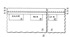
Fig. 1 illustrates semiconductor device 10.Semiconductor device 10 is integrated circuit leads.The substrate 12 of the part that it still is entire wafer that semiconductor device 10 is included in the current fabrication stage that illustrates.Semiconductor device 10 also comprises the dopant well 14,18,20 of the part of functions circuit of various formation semiconductor device 10.Substrate comprises that also the shallow trench isolation structures (not shown) of various moulding in advance is to separate different components and to separate trap discussed here from the side.Semiconductor device 10 also comprises end oxide skin(coating) 22.
Dopant well 14,18,20 can be taked various forms.Nonvolatile memory (NVM) trap 18 forms the storage unit circuit part of Nonvolatile storage array.In shown embodiment, NVM trap 18 is p traps, and memory cell array will be present in wherein.Although peripheral components includes only high voltage (HV) device (for example cell charge/discharge devices) in some cases, but here among the embodiment of Tao Luning, peripheral components comprises the various devices that are positioned at outside the NVM memory cell array, can comprise HV device, integrated circuit lead I/O (I/O) device and low-voltage (LV) device (as logical device).High voltage (HV) trap 14 is formed for programming and wipes the circuit part (as high voltage transistor) of each unit of nvm array.Shown HV trap 14 is n traps.Replaceable or additionally, semiconductor device can comprise HV p trap in dark n type isolation well.I/O trap 20 forms the I/O circuit part of semiconductor device 10.Shown I/O trap 20 is n traps.Replaceable or additionally, semiconductor device can comprise I/O p trap in dark n type isolation well.In one embodiment, I/O trap 20 is dual gate oxide (DGO) traps.
With reference to Fig. 2, (for example electric conducting material of the alloy of silicon, aluminium, gold, germanium or silicon and germanium or other type or doping or unadulterated semi-conducting material) nanocluster layer 24 for example by chemical vapor deposition technology, aerosol deposition technology, spin coating technique or self-assembling technique (as to film annealing to form nano-cluster) be formed on the oxide skin(coating) 22.In one embodiment, nano-cluster 24 is si-nanocrystals.Be used for the embodiment of nonvolatile memory at nano-cluster, this nano-cluster has the plane density that size is the 1X10^12cm^2 of 5 to 7 nanometers.In certain embodiments, the size of nano-cluster is the 10-100 dust.But nano-cluster in other embodiments can have other size and/or other density.In one embodiment, nano-cluster 24 is separated with the average distance of the mean size that is generally equal to bunch.This average distance in such embodiment greater than 4 nanometers.Although shown nano-cluster 24 has uniform size and distribution, nano-cluster 24 can have size heterogeneous and distribution heterogeneous in actual applications.Nano-cluster 24 will be used for realizing charge storage locations at the transistor of the nonvolatile memory of semiconductor device 10 (referring to Figure 16).
Deposited after the nano-cluster 24, on nanocrystal 24, formed dielectric materials layer (as silicon dioxide layer, silicon oxynitride layer, hafnium oxide layer, alumina layer, lanthana layer and lanthanum silicate layer) (for example passing through chemical vapor deposition) to form control dielectric layer 26.In one embodiment, silicon dioxide is deposited upon on the nano-cluster.Replacedly, other dielectric such as silicon oxynitride, hafnium oxide, aluminium oxide, lanthana or lanthanum silicate can be used for layer 26.In another embodiment, oxide-nitride thing-oxide (ONO) lamination of silicon dioxide, silicon nitride and silicon dioxide can be used for layer 26.In one embodiment, the thickness of dielectric layer 26 approximately is the 5-15 nanometer, but can be other thickness in other embodiments.
In certain embodiments, end dielectric layer 22, nano-cluster 24 and control dielectric layer 26 can by ion (as silicon or germanium) is injected the dielectric materials layer (not shown) and and then to this ion annealing so that form in the mode of this dielectric materials layer formation nanocrystal.In other embodiments, end dielectric layer 22, nano-cluster 24 and control dielectric layer 26 can be by forming in the mode that forms nano-cluster the oxide skin(coating) that is rich in silicon between two dielectric materials layers crystallization again.In other embodiments, nano-cluster may be embodied as a plurality of layers that are positioned on the end dielectric layer.In other embodiments, nano-cluster forms by the thin amorphous layer (as the 1-5 nanometer) of depositing nano clustered materials, wherein in annealing process subsequently the structure that produces is annealed.
With reference to Fig. 3, doped polycrystalline silicon layer 28 is formed on the dielectric layer 26.Part polysilicon layer 28 will be as the gate electrode of NVM bit location.This polysilicon layer can doped in situ (in deposition process) or mix by injecting (after deposition).Can use other gate material such as metal.After having deposited gate electrode 28, deposit anti-reflection coating (ARC).In the illustrated embodiment, silicon nitride layer 30 provides anti-reflection coating.
With reference to Fig. 4, mask layer 32 (as photoresist) is formed on the nitride layer 30.Gate stack above the mask layer 32 protection NVM traps 18, and from other zone of semiconductor device 10, expose the part of layer 30,28,26,24 and 22.Remove nitride layer 30, polysilicon layer 28, dielectric layer 26 and nanocluster layer 24 subsequently.Then also remove the part of layer 22.In one embodiment, adopt active-ion-etch to remove layer 30,28,26,24 and 22.
With reference to Fig. 5, removed mask layer 32 and exposed nitride, and the part that is exposed of remaining tunnel dielectric layer 22 also is removed to expose substrate.At tunnel dielectric layer 22 is among the embodiment of silicon dioxide, can use the hydrofluoric acid of dilution to carry out this removal by wet etching.
With reference to Fig. 6, formed high voltage device oxide layer 34.For example can be by the HV oxide skin(coating) 34 of growing of the oxidation in oxygen or steam.An exemplary oxide skin(coating) 34 is the silicon dioxide of thickness between 5 to 15 nanometers.Oxide skin(coating) 35 growth on nitride layer 30 incidentally typically has littler thickness.In this rodent oxidation step process, nitride layer 30 is as diffusion impervious layer and protect following nano-cluster 24, polysilicon layer 28 and tunnel dielectric layer 22 not by oxidation nocuously.If allow to occur, this oxidation may influence the performance of NVM device unfriendly, because the programming of nano-cluster and wipe the size of the thickness of dielectric layer 22 and nano-cluster very responsive.
Then, by injecting the low voltage device wells 37 that substrate 12 is formed for general logical circuit.Open low-voltage area by masks and then carry out traditional injection process afterwards.HV oxide skin(coating) 34 is as the sacrifical oxide of low voltage well infusion.Logic well activates by rapid thermal annealing process usually.
After forming logic well 37, on HV oxide skin(coating) 34, form the part of mask layer 36 (as photoresist), and expose the remainder of HV oxide skin(coating) with the HV oxide skin(coating) above the protection HV device well 14.
With reference to Fig. 7, use the be exposed part of the hydrofluoric acid of dilution by wet etching removal HV oxide skin(coating) 34.Oxide skin(coating) 35 is accompanied by being exposed part of layer 34 and is removed.After removing the part that is exposed of HV oxide skin(coating) 34,35, also remove mask layer 36.
With reference to Fig. 8, form I/O device oxide layer 38.Although can use additive method, oxide skin(coating) 38 is grown by the oxidation in oxygen usually.Can use such as N
2Other oxygen compound of O.An exemplary oxide layer 38 is a silicon dioxide.I/O oxide skin(coating) 38 is thinner a little than HV oxide skin(coating) 34 usually, and its thickness is between 4 to 8 nanometers.Thin oxide layer 39 growth on nitride layer 30 incidentally.HV oxide skin(coating) 34 is thickening naturally in the growth course of I/O oxide skin(coating) 38.In this oxidation step process, nano-cluster 24 below nitride layer 30 is still also protected as diffusion impervious layer and tunnel dielectric layer 22 be not by oxidation nocuously.If allow to occur, this oxidation may influence the performance of NVM device unfriendly, because the programming of nano-cluster and wipe the size of the thickness of dielectric layer 22 and nano-cluster very responsive.
With reference to Fig. 9, forming mask layer 40 (as photoresist) on the I/O oxide skin(coating) 38 with the protection part of the HV oxide skin(coating) 34 on HV device well 14 and I/O device well 20 and I/O oxide skin(coating) 38 respectively, and exposing the other parts of I/O oxide skin(coating).Then, for example utilize the wet etching of dilute hydrofluoric acid to remove the part that is exposed of I/O oxide skin(coating) 38.Be accompanied by the thin oxide layer of also removing above the nitride layer 30 39.
With reference to Figure 10, remove photoresist layer 40 from HV oxide skin(coating) 34 with above the I/O oxide skin(coating) 38.Form low-voltage (LV) oxide skin(coating) 42.Although can use additive method, oxide skin(coating) 42 typically passes through at oxygen, N
2Oxidation among O or the NO and growing.An exemplary oxide skin(coating) 42 is a silicon dioxide.LV oxide skin(coating) 42 is thinner a little than HV oxide skin(coating) 34 and I/O oxide skin(coating) 38 usually, and its thickness is between 1.5 to 3 nanometers.Extremely thin oxide skin(coating) 43 can growth on nitride layer 30 incidentally.HV oxide skin(coating) 34 and I/O oxide skin(coating) 38 can thickenings naturally in the growth course of LV oxide skin(coating) 42.In this oxidation step process, nano-cluster 24 and tunnel dielectric layer 22 below nitride layer 30 is still also protected as diffusion impervious layer are not oxidized.
With reference to Figure 11, on substrate 12, form doped polycrystalline silicon layer 44.In shown embodiment, polysilicon layer 44 is deposited on LV oxide skin(coating) 42, HV oxide skin(coating) 34, I/O oxide skin(coating) 38 and follows above the oxide skin(coating) 43.Polysilicon layer 44 parts will be as the gate electrode of HV, LV and I/O device.When polysilicon was used as the gate electrode of peripheral components and nvm array device, typically, this two-layer thickness about equally.In other embodiments, the different materials with suitable thickness can be used for the gate electrode of peripheral and nvm array.Polysilicon layer 44 can doped in situ (in deposition process) or mix by injecting (after deposition).Can use other gate material such as metal.After having deposited gate electrode 44, deposit anti-reflection coating (ARC).In the illustrated embodiment, silicon nitride layer 46 provides anti-reflection coating.
With reference to Figure 12, mask layer 48 (as photoresist) is formed on above the nitride layer 46 on the peripheral components and is used to form the pattern of the grid of this device, for example uses the anisotropic plasma etching to remove the part that is exposed of layer 44 and 46 afterwards.In this gate pattern forming process, remove polysilicon layer 44 and nitride layer 46 and cover the top part in NVM district, allow to keep the gate electrode (as the part of layer 44) of LV, HV and I/O device simultaneously.Use to floor 43 and 30 selectively the result of active-ion-etch finished basically above the nvm array district to remove layer of gate electrode material 44 and ARC floor 46, form the pattern of the gate electrode of I/O, HV and LV device simultaneously.
With reference to Figure 13, removed mask layer 48.Mask layer 50 (as photoresist) is formed on corresponding on HV trap 14, I/O trap 20, LV trap 37 and other the regional peripheral device region.This mask layer is used to form the pattern of the gate electrode of nvm array device, and is used to protect the periphery of semiconductor device 10.
With reference to Figure 14, remove the each several part plasma etching of non-selective, anisotropy, timing (for example by) of each layer that masked layer 50 exposes.For example remove the partial oxide layer 43, nitride ARC layer 30, grid layer 28, control dielectric layer 26 and the nanocluster layer 24 that are exposed.The part of tunnel dielectric layer 22 also is removed.
With reference to Figure 15, removed mask layer 50.Utilize wet etching process to remove any remaining part that is exposed of low voltage oxide layer 42, high voltage oxide layer 34, NVM tunnel dielectric layer 22 and I/O oxide skin(coating) 38.Extremely thin oxide skin(coating) 43 on NVM ARC layer 30 also is removed.At all oxides layer 34,38,42 all is among the embodiment of silicon dioxide, can adopt the hydrofluoric acid of dilution to wash and carry out this removal.
With reference to Figure 16, finish NVM unit and peripheral components.After all gate electrodes that form as described in Figure 15, form source/drain extensions, sidewall spacer and source/drain regions with the standard CMOS treatment technology.As shown in the figure, the source/drain regions and the extension of 60 and 62 expression HV devices, the source/drain regions and the extension of 64 and 66 expression NVM unit, the source/drain regions and the extension of 68 and 70 expression I/O devices, the source/drain regions and the extension of 72 and 74 expression LV devices.Sidewall spacer 52 is corresponding to the HV device, and sidewall spacer 54 is corresponding to the NVM unit component, and sidewall spacer 56 is corresponding to the I/O device, and sidewall spacer 58 is corresponding to the LV device.
In another embodiment, after the LV oxide skin(coating) 42 that forms as shown in figure 10, can on substrate 12, form doped polycrystalline silicon layer 44 as shown in figure 17.In shown embodiment, polysilicon layer 44 is deposited on LV oxide skin(coating) 42, HV oxide skin(coating) 34, I/O oxide skin(coating) 38 and follows on the oxide skin(coating) 43.The part of polysilicon layer 44 will be as the gate electrode of HV, LV and I/O device.In this embodiment, do not need anti-reflection coating (ARC), because etching subsequently is at large tracts of land rather than at critical dimension in this stage.
With reference to Figure 18, in HV, I/O and LV district, form mask layer 80 (as photoresist) and form pattern, and expose the NVM well area.In Figure 19, utilize for example dry ecthing, wet etching or its to be combined in etching polysilicon layer 44 on the NVM zone, thin oxide layer 43 and nitride layer 30.In one embodiment, when changing, the chemical property that detects material stops etching.In Figure 20, remove mask layer 80 (for example peeling off (piranha resist strip)) by plasma ash technology or peroxosulphuric resist, ARC layer 82 conformally is deposited on polysilicon layer 44 and 28.In an illustrated embodiment, silicon nitride is used to provide anti-reflection coating.In Figure 21, in HV, I/O, LV, NVM district, form mask layer 84.In Figure 22, carry out dry ecthing to remove ARC layer 82 and following polysilicon layer 44 and 28, exposed dielectric layer 26,34,38,42 thus.In Figure 23, remove mask layer 84 (as above about the discussion of mask layer 80), and partly continue to form gate electrode by removing being exposed of (for example etching) dielectric layer 26,34,38,42 and layer 24.After removing ARC layer 82, continue to handle to be similar to the mode of describing according to Figure 16.This interchangeable embodiment provides has only an advantage with critical dimension in two masks, the advantage that this advantage can be brought cost and make.
Above-mentioned explanation is intended to describe at least one embodiment of the present invention.Above-mentioned explanation is not to limit scope of the present invention.And scope of the present invention limits in the following claims.Therefore other embodiments of the invention have comprised other distortion, modification, increase and/or the improvement of above-mentioned explanation.
In one embodiment, provide a kind of method that is used to form nanocluster charge storage device.Substrate is provided.This substrate have first dopant well related with nanocluster charge storage device and with the second related dopant well of the semiconductor device that does not have nano-cluster.Form the first grid lamination, it covers on first dopant well, and has first conductive gate material layer that forms the gate electrode in the first grid lamination.The a plurality of nano-clusters that are embedded in the first grid dielectric layer of first conductive gate material layer overlies.First conductive gate material layer is positioned under a part of second conductive gate material layer.Use covers a part second conductive gate material layer on second dopant well as the gate electrode in the second grid lamination, forms the second grid lamination that covers on second dopant well.Remove the part that covers in second conductive gate material layer on first conductive gate material layer.
In another embodiment, by covering all zone and etching second conductive gate material layer optionally, remove that part that covers first conductive gate material layer in second conductive gate material layer away from first dopant well.In another embodiment, utilize the polysilicon, the metal or metal alloy that mix to form first conductive gate material layer and second conductive gate material layer.In another embodiment, first conductive gate material layer is to realize with the material that is different from second conductive gate material layer.
In another embodiment, form the first grid dielectric layer by forming the gate oxide level and the second grid oxide skin(coating) that cover and surround nanocluster layer.The first grid dielectric layer and first conductive gate material layer form and cover on first dopant well and second dopant well.The combination that utilizes wet etching and dry ecthing optionally etching first conductive gate material layer, first grid dielectric layer and nanocluster layer from the zone that covers second dopant well.
In another embodiment, form the second grid lamination by forming the second grid dielectric layer and second conductive gate material layer that cover a part of second dopant well.The second conductive gate material layer overlies second grid dielectric layer.In another embodiment, the second grid dielectric layer is formed by silicon dioxide or silicon oxynitride.
In another embodiment, nitride layer is formed in the first grid lamination and covers first conductive gate material, and between a part of first conductive gate material and second conductive gate material.Oxide skin(coating) is formed on this nitride layer and with this nitride layer physics and contacts.This nitride layer and oxide skin(coating) are used as etch stop layer when removing second conductive gate material.This nitride layer is used as anti-reflection coating when also forming gate electrode in the first grid lamination.
In another embodiment, the first grid dielectric layer is formed by oxide that comprises compound at least a in hafnium, lanthanum, aluminium, the silicon or nitrogen oxide.
In another embodiment, being embedded in a plurality of nano-clusters in the first grid dielectric layer that covers first dopant well and second dopant well is to mix or unadulterated semiconductor nanocrystal layer, metal nanocrystal layer, two or more doping or the nanocrystal layer or the metal alloy nanocrystal layer of doped semiconductor do not form by forming.
In another embodiment, first source electrode and first drain electrode are formed on around the first grid lamination and the first dopant well inside, to form charge storage device as nonvolatile memory (NVM) transistor.Second source electrode and second drain electrode are formed on around the second grid lamination and the second dopant well inside, to form periphery transistor.
In another embodiment, form semiconductor device from the second grid lamination.This semiconductor device makes it possible to nanocluster charge storage device charging and discharge.
In another embodiment, a kind of method may further comprise the steps: substrate is provided; In substrate, form first dopant well and second dopant well; Formation is embedded in the nanocluster layer in the first grid dielectric layer that covers first dopant well and second dopant well; Form first conductive gate material layer that covers nanocluster layer; Form the nitride layer that covers first conductive gate material layer; Remove nitride layer, first conductive gate material layer, nanocluster layer in the zone of first dopant well and form the storage layer stack that covers first dopant well by forming pattern and never covering; Form the second grid dielectric layer that covers second dopant well, this second grid dielectric layer does not have nano-cluster; Form second conductive gate material layer that covers second grid dielectric layer and storage layer stack; Form the anti-reflection coating that covers second conductive gate material layer; When from storage layer stack, removing second conductive gate material layer, second conductive gate material layer is carried out pattern formation have the first grid lamination of second conductive gate material layer as its gate electrode with formation; Form the second grid lamination that covers first dopant well by removing a part of storage layer stack, this second grid lamination utilizes first conductive gate material layer as the gate electrode with charge storage device of nano-cluster.
In another embodiment, this method is further comprising the steps of: drain to form transistor with inner first source electrode and first that forms of second dopant well around the first grid lamination; Around the second grid lamination, drain to finish the formation of charge storage device with inner second source electrode and second that forms of first dopant well.
In another embodiment, this method also comprises step: first conductive gate material layer that forms doped polycrystalline silicon, metal or metal alloy.
In another embodiment, this method also comprises step: second conductive gate material layer (44) that forms doped polycrystalline silicon, metal or metal alloy.
In another embodiment, this method also comprises step: form the nanocluster layer that is embedded in the first grid dielectric layer that covers first dopant well and second dopant well by forming doping or unadulterated semiconductor nanocrystal layer, metal nanocrystal layer, two or more doping or unadulterated semi-conductive nanocrystal layer or metal alloy nanocrystal layer.
In another embodiment, this method also comprises step: form the first grid dielectric layer with oxide that comprises compound at least a in hafnium, lanthanum, aluminium, the silicon or nitrogen oxide.
In another embodiment, this method also comprises step: form the second grid dielectric layer with silicon dioxide or silicon oxynitride.
In another embodiment, a kind of method that is used to form nanocluster charge storage device may further comprise the steps: provide have the memory dopant well related with nanocluster charge storage device and with the substrate of the related peripheral dopant well of the semiconductor device that does not have nano-cluster; Formation is embedded in the nanocluster layer in the first grid dielectric layer that covers this memory dopant well; Form the first grid material layer that covers nanocluster layer; Thereby nanocluster layer and first grid material layer are carried out pattern to be formed and only exists on the memory dopant well; After forming the first grid material layer, form the second grid material layer that covers peripheral dopant well and cover nanocluster layer and first grid material layer; Form the peripheral components gate stack by from the zone except the predetermined outer peripheral areas that covers peripheral dopant well, removing the second grid material layer; By being carried out pattern, the nanocluster layer of overlaying memory dopant well and first grid material layer form the nanocluster charge storage device gate stack subsequently, even wherein the first grid material layer formed before the second grid material layer, the charge storage device gate stack also forms after forming the peripheral components gate stack.
In another embodiment, this method also is included in and forms the direct etch stop layer of first grid material layer that covers in the process of removing the second grid material layer that covers the first grid material layer with endpoint detection.
In another embodiment, a kind of method that forms nanocluster charge storage device comprises: provide have the memory dopant well related with nanocluster charge storage device and with the substrate of the related peripheral dopant well of the semiconductor device that does not have nano-cluster; Formation is embedded in the nanocluster layer in the first grid dielectric layer that covers this memory dopant well; Form the first grid material layer that covers nanocluster layer; Thereby nanocluster layer and first grid material layer are carried out pattern to be formed and only exists on the memory dopant well; After forming the first grid material layer, form the second grid material layer that covers peripheral dopant well and cover nanocluster layer and first grid material layer; From the zone except the predetermined outer peripheral areas that covers peripheral dopant well, remove the second grid material layer; Utilize mask optionally to form peripheral components gate stack and nano-cluster electric charge storage grid in the substantially the same moment.
A lot of device described herein can be conceptualized as to have and be used for the control end that flow of Control current between the first current practice end and the second current practice end.An example of this device is a transistor.The appropraite condition of transistorized control end causes electric current to flow to the second current practice end/flow to the first current practice end from the second current practice end from the first current practice end.Equally, although field-effect transistor (FET) is described as having drain electrode, grid and source electrode usually, in most of this devices, drains and to exchange with source electrode.This is normally symmetrical because of transistorized layout and semiconductor processes.
Because above-mentioned detailed description is exemplary, when describing " embodiment " the expression exemplary embodiment.Therefore, term " " use in this article is not to represent to have one also only to have an embodiment can have described feature.But other a lot of embodiment can and have exemplary " embodiment " described feature usually.Therefore, as what use above, when describing in the linguistic context of an embodiment when of the present invention, this embodiment is a plurality of in may embodiment one of the present invention.
Though for preventing to misread " embodiment " use in this detailed description has been described above, those skilled in the art is to be understood that if will introduce the claim element of specific quantity in claims, such intention will clearly be write exactly in this claim, is not having do not have under such situation about expressing or do not plan that such restriction is arranged.For example in claims, be described to have " one " feature when right requires element, this just means that this element will be restricted to one a described feature is also only arranged.In addition, when in claims the claim element being described as comprising " one (a) " feature, this does not also mean that this element is restricted to one a described feature is also only arranged.In addition, the claim that relates to device or method that for example, comprises " one " feature comprises one or more features of discussing.That is to say,, relate to the claim of this device or method no matter be that device or method all comprise other similar characteristics because device or the method discussed comprise a feature." one " that the applicant is used in the feature of the claim of this employing is nonrestrictive, introductory article, and is identical with the past explanation adopted of a lot of court, although also can find opposite unusual case or precedent.Similarly, when in claims, the claim element is described as comprising above-mentioned feature (as " and as described in " feature), then show can not be only identical use by definite article just this element is limited to one and have only a described feature.
In addition, guided bone phrase in claims should not be interpreted as representing that as " at least one " and " one or more " another claim element of introducing by indefinite article requires any specific rights that comprises the claim element of being introduced to be restricted to the invention that only comprises a this element, even some claims comprise guided bone phrase " one or more " or " at least one " and indefinite article.For the usage of definite article too.
Based on the instruction here, those skilled in the art can easily implement to provide structure disclosed herein and the needed step of method, and can understanding process parameter, material, size and sequence of steps just provide as example, can change in order to reach desired results, and make the interior revision of the scope of the invention.Variation of the embodiment disclosed herein and revision can be made based on description given here, and can not break away from the spirit and scope of the present invention that provide in claims.
Though illustrate and described specific embodiments of the invention, be easy to use various modifications to one skilled in the art, replace structure and equivalent and do not break away from the scope of protection of present invention based on the instruction here.Therefore, appended claims in its encompasses all such changes in true spirit of the present invention and scope, the revision or the like.In addition, should be appreciated that the present invention only is subjected to the restriction of claims.Above-mentioned explanation is not the inventory completely that will present the embodiment of the invention.Unless whether clear expression the, otherwise each example that presents here all is the example of non-limiting or nonexcludability be no matter expressed non-limiting, nonexcludability or similar term simultaneously in each example.Although attempt to sketch the contours of some exemplary embodiments and exemplary variations thereof at this, other embodiment and/or distortion are also in the scope of the present invention that claims limited.
Claims (12)
1. method that is used to form nanocluster charge storage device comprises:
Provide have first dopant well related with nanocluster charge storage device and with the substrate of related second dopant well of the semiconductor device that does not have nano-cluster;
Form the first grid lamination, this first grid lamination covers on first dopant well and has first conductive gate material layer that forms the gate electrode in the first grid lamination, a plurality of nano-clusters that are embedded in the first grid dielectric layer of first conductive gate material layer overlies;
Form the second grid lamination that covers second dopant well, wherein use the part that covers second dopant well in second conductive gate material layer as the gate electrode in the second grid lamination, remove the part on first conductive gate material layer that covers in second conductive gate material layer in the first grid lamination.
2. method according to claim 1 also comprises:
By covering all zone and described second conductive gate material layer of etching optionally, remove that part that covers described first conductive gate material layer in second conductive gate material layer away from described first dopant well.
3. method according to claim 1 also comprises:
Utilize the polysilicon, the metal or metal alloy that mix to form described first conductive gate material layer and described second conductive gate material layer.
4. method according to claim 3 also comprises:
Realize described first conductive gate material layer with the material that is different from second conductive gate material layer.
5. method according to claim 1 also comprises:
Form the first grid dielectric layer, described first grid dielectric layer comprises the second grid oxide skin(coating) on first grid oxide skin(coating) and the described first grid oxide skin(coating), wherein the second grid oxide skin(coating) covers and surrounds described nanocluster layer, and the wherein said first grid dielectric layer and first conductive gate material layer form and cover on first dopant well and second dopant well;
The combination that utilizes wet etching and dry ecthing optionally etching first conductive gate material layer, first grid dielectric layer and nanocluster layer from the zone that covers second dopant well.
6. method according to claim 1 also comprises:
Form described second grid lamination, this second grid dielectric layer of described second conductive gate material layer overlies by forming the second grid dielectric layer and described second conductive gate material layer that cover a part of second dopant well.
7. method according to claim 6 also comprises:
Form described second grid dielectric layer by silicon dioxide or silicon oxynitride.
8. method according to claim 1 also comprises:
Form nitride layer in the first grid lamination, this nitride layer covers described first conductive gate material, and between a part of first conductive gate material and second conductive gate material;
Form the oxide skin(coating) that covers this nitride layer and contact with this nitride layer physics, this nitride layer and oxide skin(coating) when removing described second conductive gate material as etch stop layer, this nitride layer also during the gate electrode in forming described first grid lamination as anti-reflection coating.
9. method according to claim 1 also comprises:
Form described first grid dielectric layer by oxide that comprises compound at least a in hafnium, lanthanum, aluminium, the silicon or nitrogen oxide.
10. method according to claim 1 also comprises:
Form a plurality of nano-clusters that are embedded in the described first grid dielectric layer that covers described first dopant well and second dopant well by forming doping or unadulterated semiconductor nanocrystal layer, metal nanocrystal layer, two or more doping or unadulterated semi-conductive nanocrystal layer or metal alloy nanocrystal layer.
11. method according to claim 1 also comprises:
Around described first grid lamination, drain, to form charge storage device as nonvolatile memory (NVM) transistor with inner first source electrode and first that forms of described first dopant well;
Around described second grid lamination, drain, to form periphery transistor with inner second source electrode and second that forms of described second dopant well.
12. method according to claim 1 also comprises:
Form semiconductor device from described second grid lamination, this semiconductor device makes it possible to nanocluster charge storage device charging and discharge.
Applications Claiming Priority (2)
| Application Number | Priority Date | Filing Date | Title |
|---|---|---|---|
| US10/876,820 US7091130B1 (en) | 2004-06-25 | 2004-06-25 | Method of forming a nanocluster charge storage device |
| US10/876,820 | 2004-06-25 |
Publications (2)
| Publication Number | Publication Date |
|---|---|
| CN101010785A CN101010785A (en) | 2007-08-01 |
| CN100435286C true CN100435286C (en) | 2008-11-19 |
Family
ID=35784282
Family Applications (1)
| Application Number | Title | Priority Date | Filing Date |
|---|---|---|---|
| CNB2005800210850A Expired - Fee Related CN100435286C (en) | 2004-06-25 | 2005-05-11 | Method of forming a nanocluster charge storage device |
Country Status (6)
| Country | Link |
|---|---|
| US (1) | US7091130B1 (en) |
| EP (1) | EP1759405A4 (en) |
| JP (1) | JP2008504679A (en) |
| CN (1) | CN100435286C (en) |
| TW (1) | TWI375318B (en) |
| WO (1) | WO2006007069A2 (en) |
Families Citing this family (35)
| Publication number | Priority date | Publication date | Assignee | Title |
|---|---|---|---|---|
| US7588988B2 (en) | 2004-08-31 | 2009-09-15 | Micron Technology, Inc. | Method of forming apparatus having oxide films formed using atomic layer deposition |
| US7361543B2 (en) * | 2004-11-12 | 2008-04-22 | Freescale Semiconductor, Inc. | Method of forming a nanocluster charge storage device |
| KR100688504B1 (en) * | 2004-11-15 | 2007-03-02 | 삼성전자주식회사 | Manufacturing method of non-volatile device utilizing implantation process and device thereby |
| US20060131633A1 (en) * | 2004-12-21 | 2006-06-22 | Micron Technology, Inc. | Integrated two device non-volatile memory |
| US7183159B2 (en) * | 2005-01-14 | 2007-02-27 | Freescale Semiconductor, Inc. | Method of forming an integrated circuit having nanocluster devices and non-nanocluster devices |
| US7662729B2 (en) | 2005-04-28 | 2010-02-16 | Micron Technology, Inc. | Atomic layer deposition of a ruthenium layer to a lanthanide oxide dielectric layer |
| US7572695B2 (en) | 2005-05-27 | 2009-08-11 | Micron Technology, Inc. | Hafnium titanium oxide films |
| US7927948B2 (en) | 2005-07-20 | 2011-04-19 | Micron Technology, Inc. | Devices with nanocrystals and methods of formation |
| US7575978B2 (en) | 2005-08-04 | 2009-08-18 | Micron Technology, Inc. | Method for making conductive nanoparticle charge storage element |
| KR100698086B1 (en) * | 2005-12-29 | 2007-03-23 | 동부일렉트로닉스 주식회사 | Method for fabricating of semiconductor device |
| US7560769B2 (en) | 2006-08-03 | 2009-07-14 | Micron Technology, Inc. | Non-volatile memory cell device and methods |
| US7955935B2 (en) | 2006-08-03 | 2011-06-07 | Micron Technology, Inc. | Non-volatile memory cell devices and methods |
| US8093680B1 (en) * | 2006-09-14 | 2012-01-10 | Spansion Llc | Metal-insulator-metal-insulator-metal (MIMIM) memory device |
| US7687349B2 (en) * | 2006-10-30 | 2010-03-30 | Atmel Corporation | Growth of silicon nanodots having a metallic coating using gaseous precursors |
| FR2910176B1 (en) | 2006-12-15 | 2009-10-23 | Commissariat Energie Atomique | METHOD FOR PRODUCING A DEVICE BASED ON NANOCRYSTALS COATED WITH A CVD-BASED NITRIDE LAYER |
| US7763511B2 (en) * | 2006-12-29 | 2010-07-27 | Intel Corporation | Dielectric barrier for nanocrystals |
| US7816211B2 (en) * | 2007-01-26 | 2010-10-19 | Freescale Semiconductor, Inc. | Method of making a semiconductor device having high voltage transistors, non-volatile memory transistors, and logic transistors |
| US8128626B2 (en) * | 2007-04-24 | 2012-03-06 | Flexfix, Llc | System and method for delivery conformation and removal of intramedullary bone fixation devices |
| US9299568B2 (en) | 2007-05-25 | 2016-03-29 | Cypress Semiconductor Corporation | SONOS ONO stack scaling |
| US8614124B2 (en) | 2007-05-25 | 2013-12-24 | Cypress Semiconductor Corporation | SONOS ONO stack scaling |
| US8367506B2 (en) | 2007-06-04 | 2013-02-05 | Micron Technology, Inc. | High-k dielectrics with gold nano-particles |
| US7846793B2 (en) * | 2007-10-03 | 2010-12-07 | Applied Materials, Inc. | Plasma surface treatment for SI and metal nanocrystal nucleation |
| US9431549B2 (en) | 2007-12-12 | 2016-08-30 | Cypress Semiconductor Corporation | Nonvolatile charge trap memory device having a high dielectric constant blocking region |
| US7871886B2 (en) * | 2008-12-19 | 2011-01-18 | Freescale Semiconductor, Inc. | Nanocrystal memory with differential energy bands and method of formation |
| US7799634B2 (en) * | 2008-12-19 | 2010-09-21 | Freescale Semiconductor, Inc. | Method of forming nanocrystals |
| US8071453B1 (en) | 2009-04-24 | 2011-12-06 | Cypress Semiconductor Corporation | Method of ONO integration into MOS flow |
| US9102522B2 (en) | 2009-04-24 | 2015-08-11 | Cypress Semiconductor Corporation | Method of ONO integration into logic CMOS flow |
| US8202778B2 (en) * | 2010-08-31 | 2012-06-19 | Freescale Semiconductor, Inc. | Patterning a gate stack of a non-volatile memory (NVM) with simultaneous etch in non-NVM area |
| US8679912B2 (en) * | 2012-01-31 | 2014-03-25 | Freescale Semiconductor, Inc. | Semiconductor device having different non-volatile memories having nanocrystals of differing densities and method therefor |
| US9230977B2 (en) * | 2013-06-21 | 2016-01-05 | Taiwan Semiconductor Manufacturing Company, Ltd. | Embedded flash memory device with floating gate embedded in a substrate |
| US8883624B1 (en) | 2013-09-27 | 2014-11-11 | Cypress Semiconductor Corporation | Integration of a memory transistor into high-K, metal gate CMOS process flow |
| JP5732574B2 (en) * | 2014-04-14 | 2015-06-10 | ルネサスエレクトロニクス株式会社 | Manufacturing method of semiconductor device |
| US9218978B1 (en) * | 2015-03-09 | 2015-12-22 | Cypress Semiconductor Corporation | Method of ONO stack formation |
| CN107978606B (en) * | 2017-11-20 | 2020-08-25 | 上海华力微电子有限公司 | Embedded flash memory process integration method |
| TWI704648B (en) * | 2019-11-20 | 2020-09-11 | 華邦電子股份有限公司 | Method for manufacturing memory device |
Citations (3)
| Publication number | Priority date | Publication date | Assignee | Title |
|---|---|---|---|---|
| US6444545B1 (en) * | 2000-12-19 | 2002-09-03 | Motorola, Inc. | Device structure for storing charge and method therefore |
| US6503800B2 (en) * | 2000-06-19 | 2003-01-07 | Nec Corporation | Manufacturing method of semiconductor device having different gate oxide thickness |
| US20030222306A1 (en) * | 2002-05-30 | 2003-12-04 | Alexander Hoefler | Method of forming a semiconductor device in a semiconductor layer and structure thereof |
Family Cites Families (15)
| Publication number | Priority date | Publication date | Assignee | Title |
|---|---|---|---|---|
| TW420874B (en) * | 1998-05-04 | 2001-02-01 | Koninkl Philips Electronics Nv | Method of manufacturing a semiconductor device |
| JP2000077618A (en) * | 1998-06-15 | 2000-03-14 | Mitsubishi Electric Corp | Semiconductor device and its manufacture |
| DE69942862D1 (en) * | 1999-12-06 | 2010-11-25 | St Microelectronics Srl | Non-volatile floating gate storage cell manufacturing process and control circuit |
| US6320784B1 (en) | 2000-03-14 | 2001-11-20 | Motorola, Inc. | Memory cell and method for programming thereof |
| US6297095B1 (en) | 2000-06-16 | 2001-10-02 | Motorola, Inc. | Memory device that includes passivated nanoclusters and method for manufacture |
| JP4096507B2 (en) * | 2000-09-29 | 2008-06-04 | 富士通株式会社 | Manufacturing method of semiconductor device |
| JP4322477B2 (en) * | 2001-06-28 | 2009-09-02 | 株式会社東芝 | Manufacturing method of semiconductor device |
| JP3993438B2 (en) * | 2002-01-25 | 2007-10-17 | 株式会社ルネサステクノロジ | Semiconductor device |
| JP2003218245A (en) * | 2002-01-25 | 2003-07-31 | Sony Corp | Method of manufacturing non-volatile semiconductor memory device |
| JP2003309182A (en) | 2002-04-17 | 2003-10-31 | Hitachi Ltd | Method of manufacturing semiconductor device and semiconductor device |
| US7189606B2 (en) * | 2002-06-05 | 2007-03-13 | Micron Technology, Inc. | Method of forming fully-depleted (FD) SOI MOSFET access transistor |
| JP2004104009A (en) * | 2002-09-12 | 2004-04-02 | Fujitsu Ltd | Semiconductor device and manufacturing method thereof |
| JP4477886B2 (en) * | 2003-04-28 | 2010-06-09 | 株式会社ルネサステクノロジ | Manufacturing method of semiconductor device |
| US6958265B2 (en) * | 2003-09-16 | 2005-10-25 | Freescale Semiconductor, Inc. | Semiconductor device with nanoclusters |
| US7098502B2 (en) | 2003-11-10 | 2006-08-29 | Freescale Semiconductor, Inc. | Transistor having three electrically isolated electrodes and method of formation |
-
2004
- 2004-06-25 US US10/876,820 patent/US7091130B1/en active Active
-
2005
- 2005-05-11 EP EP05782558A patent/EP1759405A4/en not_active Withdrawn
- 2005-05-11 JP JP2007518062A patent/JP2008504679A/en active Pending
- 2005-05-11 WO PCT/US2005/016252 patent/WO2006007069A2/en not_active Application Discontinuation
- 2005-05-11 CN CNB2005800210850A patent/CN100435286C/en not_active Expired - Fee Related
- 2005-06-10 TW TW094119327A patent/TWI375318B/en not_active IP Right Cessation
Patent Citations (3)
| Publication number | Priority date | Publication date | Assignee | Title |
|---|---|---|---|---|
| US6503800B2 (en) * | 2000-06-19 | 2003-01-07 | Nec Corporation | Manufacturing method of semiconductor device having different gate oxide thickness |
| US6444545B1 (en) * | 2000-12-19 | 2002-09-03 | Motorola, Inc. | Device structure for storing charge and method therefore |
| US20030222306A1 (en) * | 2002-05-30 | 2003-12-04 | Alexander Hoefler | Method of forming a semiconductor device in a semiconductor layer and structure thereof |
Also Published As
| Publication number | Publication date |
|---|---|
| CN101010785A (en) | 2007-08-01 |
| EP1759405A4 (en) | 2008-11-12 |
| WO2006007069A3 (en) | 2007-04-12 |
| TWI375318B (en) | 2012-10-21 |
| TW200612548A (en) | 2006-04-16 |
| US7091130B1 (en) | 2006-08-15 |
| WO2006007069A2 (en) | 2006-01-19 |
| EP1759405A2 (en) | 2007-03-07 |
| JP2008504679A (en) | 2008-02-14 |
| US20060194438A1 (en) | 2006-08-31 |
Similar Documents
| Publication | Publication Date | Title |
|---|---|---|
| CN100435286C (en) | Method of forming a nanocluster charge storage device | |
| US7763928B2 (en) | Multi-time programmable memory | |
| US7361543B2 (en) | Method of forming a nanocluster charge storage device | |
| US7416945B1 (en) | Method for forming a split gate memory device | |
| US7838363B2 (en) | Method of forming a split gate non-volatile memory cell | |
| US7118972B2 (en) | Method of manufacture of a semiconductor device | |
| US7439134B1 (en) | Method for process integration of non-volatile memory cell transistors with transistors of another type | |
| KR19980070519A (en) | Method for integrating nonvolatile memory and logic components into a single sub-0.3 micron fabrication process for embedded nonvolatile memory | |
| US10923601B2 (en) | Charge trapping split gate device and method of fabricating same | |
| TW201637201A (en) | Non-volatile memory unit and method for manufacturing the same | |
| US7479429B2 (en) | Split game memory cell method | |
| US8877585B1 (en) | Non-volatile memory (NVM) cell, high voltage transistor, and high-K and metal gate transistor integration | |
| CN108010915B (en) | Floating gate type flash memory SAB production method and floating gate type flash memory structure | |
| US7846790B2 (en) | Method of fabricating semiconductor device having multiple gate dielectric layers and semiconductor device fabricated thereby | |
| KR100655432B1 (en) | Non-volatile memory device and method of fabricating the same | |
| CN110164865B (en) | Method for manufacturing embedded flash memory | |
| US7183158B2 (en) | Method of fabricating a non-volatile memory | |
| CN101587863B (en) | Polysilicon grid etching method for flash memory based on SONOS and device | |
| CN101154631A (en) | Method of manufacturing flash memory device | |
| CN109524407B (en) | Memory and manufacturing method thereof | |
| KR100536799B1 (en) | semiconductor device and fabricating method thereof | |
| KR101151035B1 (en) | / device and manufacturing method of flash or eeprom having excellent on/off characteristics | |
| CN114864587A (en) | Embedded flash memory and preparation method thereof | |
| KR20080092555A (en) | Method for fabricating of non-volatile memory device | |
| KR20070023770A (en) | Method of forming a nanocluster charge storage device |
Legal Events
| Date | Code | Title | Description |
|---|---|---|---|
| C06 | Publication | ||
| PB01 | Publication | ||
| C10 | Entry into substantive examination | ||
| SE01 | Entry into force of request for substantive examination | ||
| C14 | Grant of patent or utility model | ||
| GR01 | Patent grant | ||
| CF01 | Termination of patent right due to non-payment of annual fee | ||
| CF01 | Termination of patent right due to non-payment of annual fee |
Granted publication date: 20081119 Termination date: 20160511 |