WO2009128359A1 - Glass laminate, display panel with support, method for producing glass laminate and method for manufacturing display panel with support - Google Patents
Glass laminate, display panel with support, method for producing glass laminate and method for manufacturing display panel with support Download PDFInfo
- Publication number
- WO2009128359A1 WO2009128359A1 PCT/JP2009/057084 JP2009057084W WO2009128359A1 WO 2009128359 A1 WO2009128359 A1 WO 2009128359A1 JP 2009057084 W JP2009057084 W JP 2009057084W WO 2009128359 A1 WO2009128359 A1 WO 2009128359A1
- Authority
- WO
- WIPO (PCT)
- Prior art keywords
- glass substrate
- resin layer
- thin glass
- outer frame
- main surface
- Prior art date
Links
Images


Classifications
-
- B—PERFORMING OPERATIONS; TRANSPORTING
- B32—LAYERED PRODUCTS
- B32B—LAYERED PRODUCTS, i.e. PRODUCTS BUILT-UP OF STRATA OF FLAT OR NON-FLAT, e.g. CELLULAR OR HONEYCOMB, FORM
- B32B17/00—Layered products essentially comprising sheet glass, or glass, slag, or like fibres
- B32B17/06—Layered products essentially comprising sheet glass, or glass, slag, or like fibres comprising glass as the main or only constituent of a layer, next to another layer of a specific material
- B32B17/10—Layered products essentially comprising sheet glass, or glass, slag, or like fibres comprising glass as the main or only constituent of a layer, next to another layer of a specific material of synthetic resin
-
- B—PERFORMING OPERATIONS; TRANSPORTING
- B32—LAYERED PRODUCTS
- B32B—LAYERED PRODUCTS, i.e. PRODUCTS BUILT-UP OF STRATA OF FLAT OR NON-FLAT, e.g. CELLULAR OR HONEYCOMB, FORM
- B32B7/00—Layered products characterised by the relation between layers; Layered products characterised by the relative orientation of features between layers, or by the relative values of a measurable parameter between layers, i.e. products comprising layers having different physical, chemical or physicochemical properties; Layered products characterised by the interconnection of layers
- B32B7/04—Interconnection of layers
- B32B7/06—Interconnection of layers permitting easy separation
-
- G—PHYSICS
- G02—OPTICS
- G02F—OPTICAL DEVICES OR ARRANGEMENTS FOR THE CONTROL OF LIGHT BY MODIFICATION OF THE OPTICAL PROPERTIES OF THE MEDIA OF THE ELEMENTS INVOLVED THEREIN; NON-LINEAR OPTICS; FREQUENCY-CHANGING OF LIGHT; OPTICAL LOGIC ELEMENTS; OPTICAL ANALOGUE/DIGITAL CONVERTERS
- G02F1/00—Devices or arrangements for the control of the intensity, colour, phase, polarisation or direction of light arriving from an independent light source, e.g. switching, gating or modulating; Non-linear optics
- G02F1/01—Devices or arrangements for the control of the intensity, colour, phase, polarisation or direction of light arriving from an independent light source, e.g. switching, gating or modulating; Non-linear optics for the control of the intensity, phase, polarisation or colour
- G02F1/13—Devices or arrangements for the control of the intensity, colour, phase, polarisation or direction of light arriving from an independent light source, e.g. switching, gating or modulating; Non-linear optics for the control of the intensity, phase, polarisation or colour based on liquid crystals, e.g. single liquid crystal display cells
- G02F1/133—Constructional arrangements; Operation of liquid crystal cells; Circuit arrangements
- G02F1/1333—Constructional arrangements; Manufacturing methods
- G02F1/133302—Rigid substrates, e.g. inorganic substrates
Definitions
- the present invention includes a glass laminate including a glass substrate used for a liquid crystal display device, an organic EL display device and the like, a display device-equipped panel including the same, a display device panel formed using the same, and the display device panel
- the present invention relates to a display device, a glass laminate, and a method for manufacturing a display device panel.
- LCD liquid crystal display devices
- OLED organic EL display devices
- weight reduction and thinning of display devices are important issues.
- the glass substrate is etched using hydrofluoric acid or the like, and further physically polished as necessary. A thinning method is performed.
- the glass substrate is thinned by performing an etching process or the like before forming the display device member on the surface of the glass substrate, the strength of the glass substrate is lowered and the amount of deflection is increased. Therefore, the problem that it cannot process in the existing manufacturing line arises.
- the glass substrate is thinned by performing an etching process after forming the display device member on the surface of the glass substrate, the fineness formed on the surface of the glass substrate in the process of forming the display device member on the surface of the glass substrate. A problem of obvious scratches, that is, a problem of generation of etch pits occurs.
- a thin glass substrate (hereinafter also referred to as “thin glass substrate”) is referred to as another glass substrate (hereinafter also referred to as “supporting glass substrate”).
- another glass substrate hereinafter also referred to as “supporting glass substrate”.
- Patent Document 1 a glass substrate for products and a reinforcing glass substrate are bonded and integrated using electrostatic adsorption force or vacuum adsorption force between the glass substrates, and a display device using the product glass substrate is disclosed.
- Patent Document 2 describes a method for manufacturing a liquid crystal display device in which the ends of a substrate and a support of a liquid crystal display device are bonded using a glass frit adhesive, and then an electrode pattern or the like is formed.
- Patent Document 3 describes a method for manufacturing a substrate for a display device, which includes a step of irradiating a laser beam to at least the vicinity of the peripheral surface of two glass substrates to fuse the two glass substrates. .
- substrate transfer is performed by attaching a substrate to a substrate transfer jig in which an adhesive layer is provided on a support, and transferring the substrate transfer jig through a manufacturing process of a liquid crystal display element.
- a manufacturing method of a liquid crystal display device is described in which liquid crystal display element formation processing is sequentially performed on a substrate attached to a jig for use, and the substrate is peeled off from the substrate carrying jig after completing a predetermined process.
- Patent Document 5 discloses that an electrode substrate for a liquid crystal display element is subjected to a predetermined process on the electrode substrate for a liquid crystal display element using a jig in which an ultraviolet curable pressure-sensitive adhesive is provided on a support, and then cured with an ultraviolet ray.
- a method for producing a liquid crystal display element comprising: irradiating a mold adhesive with ultraviolet rays to reduce the adhesive strength of the ultraviolet curable adhesive and peeling the liquid crystal display element electrode substrate from the jig.
- Patent Document 6 describes a transport method in which a thin plate is temporarily fixed to a support plate with an adhesive material, a peripheral portion of the adhesive material is sealed with a seal material, and the support plate on which the thin plate is temporarily fixed is transported. .
- Patent Document 7 discloses a thin glass laminate obtained by laminating a thin glass substrate and a supporting glass substrate, and the thin glass and the supporting glass have easy peelability and non-adhesiveness.
- a thin glass laminate characterized by being laminated via a silicone resin layer is described.
- Patent Document 8 discloses that a protective glass substrate and a TFT array substrate are laminated in advance using a release paper silicone, and the protective glass substrate is peeled after the display device is assembled.
- the thin glass laminated body as described in patent document 7 may generate
- the gas can be generated even during heat treatment at a relatively low temperature of about 100 to 350 ° C. The generation of the gas is not preferable because it may contaminate the vacuum processing process equipment and the like.
- the heat treatment temperature is higher, for example, when it exceeds about 400 ° C., the end portion of the silicone resin layer that is in contact with the outside air may be oxidized and deteriorated. If it does so, easy peelability with a thin glass substrate will be lost, and also there exists a possibility that it may peel from a support glass substrate.
- the silicone resin layer may be whitened by oxidation, generating powdery SiO 2 , and contaminating heat treatment process equipment and the like. Further, when the resin layer deteriorates in this way, it becomes difficult to reuse the supporting glass substrate with the resin layer separated from the thin glass substrate with another thin glass substrate as a support.
- the present invention has been made in view of the above problems. In other words, it suppresses the occurrence of glass defects caused by foreign matters such as bubbles and dust mixed between glass substrates, and can be processed in an existing production line without generating etch pits. It aims at providing the glass laminated body which can be isolate
- the panel for display apparatuses aims at providing the panel for display apparatuses with a support body containing such a glass laminated body. It is another object of the present invention to provide a display device panel and a display device which are formed using such a support-equipped display device panel. Furthermore, it aims at providing the manufacturing method of the said glass laminated body or the said panel for display apparatuses with a support body.
- the present inventor has intensively studied in order to solve the above problems, and has completed the present invention.
- the present invention relates to the following (1) to (14).
- a thin glass substrate having a first main surface and a second main surface, A supporting glass substrate having a first main surface and a second main surface; and a glass laminate having a resin layer and an outer frame layer disposed between the thin glass substrate and the supporting glass substrate,
- the resin layer is fixed to the first main surface of the supporting glass substrate, has an easy peelability to the first main surface of the thin glass substrate, and is in close contact with the first main surface of the thin glass substrate.
- the method for producing a glass laminate according to (11) further includes a step of forming a display device member on the second main surface of the thin glass substrate in the obtained glass laminate. Of manufacturing panel for display device.
- the manufacturing method according to (12) further includes a separation step of separating the thin glass substrate and the supporting glass substrate in the obtained display device-equipped display device panel. Production method.
- the present invention it is possible to suppress the occurrence of glass defects due to foreign matters such as bubbles and dust mixed between glass substrates, and it is possible to process in an existing production line without generating etch pits, and to adhere thin glass
- a glass laminate that can easily separate the substrate and the resin layer can be provided.
- the glass laminated body which suppresses generation
- a preferred embodiment provides a glass laminate in which the resin layer between the thin glass substrate and the supporting glass substrate is hardly oxidized and hardly deteriorates even when the heat treatment temperature is relatively high (over 400 ° C.). can do.
- the panel for display apparatuses with a support containing such a glass laminated body can be provided.
- the display apparatus formed using such a display apparatus panel with a support body can be provided.
- the manufacturing method of the said glass laminated body or the said panel for display apparatuses with a support body can be provided.
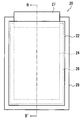
- FIG. 1 is a schematic front view showing one embodiment of the laminate of the present invention.
- FIG. 2 is a schematic cross-sectional view showing one embodiment of the laminate of the present invention.
- FIG. 3 is a schematic front view showing another embodiment of the laminate of the present invention.
- FIG. 4 is a schematic cross-sectional view showing another embodiment of the laminate of the present invention.
- FIG. 5 is a schematic cross-sectional view for explaining a method of peeling the supporting glass substrate of the laminate of the present invention.
- the present invention provides a thin glass substrate having a first main surface and a second main surface, a supporting glass substrate having a first main surface and a second main surface, and between the thin glass substrate and the supporting glass substrate.
- a glass laminate having a resin layer and an outer frame layer disposed, wherein the resin layer is fixed to a first main surface of the supporting glass substrate, and is easily peeled from the first main surface of the thin glass substrate.
- the resin layer is in close contact with the first main surface of the thin glass substrate, and the outer frame layer is on the first main surface of the support glass substrate so that the resin layer does not contact the outside air.
- a glass laminate is also referred to as “a laminate of the present invention”.
- FIG. 1 is a schematic front view showing an embodiment of the laminate of the present invention
- FIG. 2 is a cross-sectional view (schematic cross-sectional view) taken along line AA ′.
- this mode is also referred to as “mode 1”.
- the laminate 10 of the present invention has a thin glass substrate 12, a resin layer 14, an outer frame layer 16, and a supporting glass substrate 18.
- the thin glass substrate 12 and the supporting glass substrate 18 are laminated with the resin layer 14 and the outer frame layer 16 interposed therebetween. Further, as shown in FIG.
- the thin glass substrate 12, the resin layer 14, and the support glass substrate 18 are each rectangular, and the main surface area of the thin glass substrate 12 is larger than the main surface area of the resin layer 14. However, it is slightly smaller than the main surface area of the supporting glass substrate 18.
- the thin glass substrate 12 is positioned so as to be included inside the supporting glass substrate 18, and the resin layer 14 and the outer frame layer 16 are positioned so as to be included inside the thin glass substrate 12. ing.
- the outer frame layer 16 when viewed from the front, the outer frame layer 16 exists in the vicinity of the outer edge (outer region) of the thin glass substrate 12 like a frame surrounding the outer side of the resin layer 14. As shown in FIG. 2, the outer frame layer 16 is fixed to the first main surface of the thin glass substrate 12 and the first main surface of the support glass substrate 18. Therefore, the resin layer 14 existing inside thereof does not come into contact with outside air. When the outer frame layer 16 does not exist, the end surface 14 ⁇ of the resin layer 14 comes into contact with the outside air. When viewed from the front, the TFT array and the like are formed inside the outer frame layer, and the TFT array and the formation region of the outer frame layer overlap with each other so that they cannot be seen.
- an outer frame layer is formed on the first main surface of the thin glass substrate corresponding to the region excluding the effective region for forming the TFT array and the like on the second main surface of the thin glass substrate. is required. This is to prevent the TFT array or the like from being damaged by laser irradiation as will be described later.
- the resin layer 14 is fixed to the first main surface of the support glass substrate 18, and has easy peelability from the first main surface which is one main surface of the thin glass substrate 12.
- the thin glass substrate 12 is in close contact with the first main surface.
- the end surface 14 ⁇ of the resin layer 14 and the end surface 16 ⁇ on the inner side of the outer frame layer 16 are in contact with each other.
- Such a glass laminate of aspect 1 hardly generates gas during heat treatment. This is because the gas generated from the resin layer 14 does not diverge to the outside because the outer frame layer 16 exists. Moreover, if it is set as the preferable aspect mentioned later, even if the heat processing temperature is comparatively high temperature (over about 400 degreeC), the resin layer between a thin glass substrate and a support glass substrate cannot be easily oxidized, and it is hard to deteriorate. This is because the outer frame layer 16 blocks contact between the outside air and the end surface 14 ⁇ of the resin layer 14.
- the thin glass substrate will be described.
- the thickness, shape, size, physical properties (heat shrinkage, surface shape, chemical resistance, etc.), composition, etc. of the thin glass substrate are not particularly limited.
- a conventional glass substrate for a display device such as an LCD or OLED It may be the same.
- the thin glass substrate is preferably a TFT array glass substrate.
- the thickness of the thin glass substrate is preferably less than 0.7 mm, more preferably 0.5 mm or less, and further preferably 0.4 mm or less. Further, it is preferably 0.05 mm or more, more preferably 0.07 mm or more, and further preferably 0.1 mm or more.
- the shape of the thin glass is not limited, but is preferably rectangular.
- the size of the thin glass is not limited, but for example, in the case of a rectangle, it may be 100 to 2000 mm ⁇ 100 to 2000 mm, and more preferably 500 to 1000 mm ⁇ 500 to 1000 mm.
- the thickness of the thin glass is expressed by the average value of the values measured at 9 points in the plane using a laser focus displacement meter, and the size is a value obtained by measuring the short side and the long side using a steel ruler. Shall mean. The same applies to the thickness and size of the supporting glass substrate described later.
- the laminate of the present invention can easily peel the thin glass substrate and the supporting glass substrate.
- properties of the thin glass substrate such as thermal shrinkage, surface shape, chemical resistance, etc. are not particularly limited, and vary depending on the type of display device to be manufactured. Moreover, it is preferable that the thermal contraction rate of the said thin glass substrate is small. Specifically, it is preferable to use one having a linear expansion coefficient of 500 ⁇ 10 ⁇ 7 / ° C. or less, which is an index of heat shrinkage rate.
- the linear expansion coefficient is more preferably 300 ⁇ 10 ⁇ 7 / ° C. or less, more preferably 200 ⁇ 10 ⁇ 7 / ° C. or less, and more preferably 100 ⁇ 10 ⁇ 7 / ° C. or less. More preferably, it is 45 ⁇ 10 ⁇ 7 / ° C. or less. This is because a high-definition display device cannot be made if the heat shrinkage rate is large.
- a linear expansion coefficient means a thing prescribed
- the composition of the thin glass substrate may be the same as that of alkali glass or non-alkali glass, for example.
- alkali-free glass is preferable because of its low thermal shrinkage rate.
- the support glass substrate will be described.
- the supporting glass substrate supports the thin glass substrate through the resin layer and reinforces the strength of the thin glass substrate.
- the thickness, shape, size, physical properties (heat shrinkage rate, surface shape, chemical resistance, etc.), composition, etc. of the supporting glass substrate are not particularly limited.
- the thickness of a support glass substrate is not specifically limited, It is preferable that it is the thickness which can be processed with the present production line.
- the thickness is preferably 0.1 to 1.1 mm, more preferably 0.3 to 0.8 mm, and still more preferably 0.4 to 0.7 mm.
- the thickness of the supporting glass substrate and the resin layer The sum with the thickness is 0.4 mm.
- the current production line is most commonly designed to process a glass substrate having a thickness of 0.7 mm.
- the thickness of a thin glass substrate is 0.4 mm
- the supporting glass The sum of the thickness of the substrate and the thickness of the resin layer is 0.3 mm.
- the thickness of the supporting glass substrate is preferably thicker than that of the thin glass substrate.
- the shape of the supporting glass substrate is not limited, but is preferably rectangular.
- the size of the supporting glass substrate is not limited, but is preferably about the same as that of the thin glass substrate, and is slightly larger than the glass substrate (each of which is about 0.05 to 10 mm larger in the vertical direction or the horizontal direction). preferable.
- the reason is that it is easy to protect the end portion of the thin glass substrate from the contact of an alignment device such as a positioning pin at the time of manufacturing a panel for a display device, and that the thin glass substrate and the supporting glass substrate are more easily separated. Because it can.
- the supporting glass substrate may have a linear expansion coefficient that is substantially the same as or different from that of the thin glass substrate. Substantially the same is preferable in that the thin glass substrate or the supporting glass substrate is less likely to warp when the laminate of the present invention is heat-treated.
- the difference in linear expansion coefficient between the thin glass substrate and the supporting glass substrate is preferably 300 ⁇ 10 ⁇ 7 / ° C. or less, more preferably 100 ⁇ 10 ⁇ 7 / ° C. or less, and 50 ⁇ 10 ⁇ 7 / ° C. More preferably, it is not higher than ° C.
- the composition of the supporting glass substrate may be the same as that of alkali glass or non-alkali glass, for example. Among these, alkali-free glass is preferable because of its low thermal shrinkage rate.
- the resin layer will be described.
- the resin layer is fixed to the first main surface of the support glass substrate. And although the resin layer is closely_contact
- the resin layer and the thin glass substrate are not attached by the adhesive force that the adhesive has, and the force caused by the van der Waals force between the solid molecules, that is, the adhesive force. It is considered attached.
- the thickness of the resin layer is not particularly limited.
- the thickness is preferably 1 to 100 ⁇ m, more preferably 5 to 30 ⁇ m, and even more preferably 7 to 20 ⁇ m. This is because when the thickness of the resin layer is in such a range, the thin glass substrate and the resin layer are sufficiently adhered. Moreover, even if bubbles or foreign substances are present, it is possible to suppress the occurrence of distortion defects in the thin glass substrate. On the other hand, if the resin layer is too thick, it takes time and materials to form the resin layer, which is not economical.
- the thickness of the resin layer means an average value of values obtained by measuring nine points in a plane using a laser focus displacement meter. The same applies to the thickness of the outer frame layer described later.
- the resin layer may consist of two or more layers.
- the thickness of the resin layer means the total thickness of all the layers.
- the kind of resin which forms each layer may differ. The same applies to the outer frame layer described later.
- the surface tension of the surface of the resin layer relative to the first main surface of the thin glass substrate is preferably 30 mN / m or less, more preferably 25 mN / m or less, and 22 mN / m or less. Is more preferable. This is because such surface tension can be more easily peeled off from the thin glass substrate, and at the same time, the close contact with the thin glass substrate becomes sufficient.
- the resin layer is preferably made of a material having a glass transition point lower than room temperature (about 25 ° C.) or a material having no glass transition point.
- the resin layer has heat resistance.
- the glass laminate having the resin layer is subjected to heat treatment.
- the adhesiveness with a thin glass substrate will become low when the elasticity modulus of a resin layer is too high, it is unpreferable. On the other hand, if the elastic modulus is too low, the easy peelability is lowered, which is not preferable.
- the type of resin forming the resin layer is not particularly limited.
- acrylic resin, polyolefin resin, polyurethane resin, and silicone resin can be used. Two kinds of resins can be mixed and used. Of these, silicone resins are preferred. This is because the silicone resin is excellent in heat resistance and easy to peel from a thin glass substrate. It is also preferable that the silicone resin layer is not easily deteriorated even if it is treated at, for example, about 400 ° C. for about 1 hour. Further, since the silicone resin undergoes a condensation reaction with the silanol group on the surface of the supporting glass substrate, the silicone resin layer is easily fixed to the surface (first main surface) of the supporting glass substrate.
- the resin layer is preferably made of silicone for release paper among silicone resins, and is preferably a cured product thereof.
- the silicone for release paper is mainly composed of silicone containing linear dimethylpolysiloxane in the molecule.
- the resin layer formed by curing the composition containing the main agent and the crosslinking agent on the surface (first main surface) of the supporting glass substrate using a catalyst, a photopolymerization initiator, etc. has excellent easy peelability. Since it has, it is preferable. In addition, since the flexibility is high, even if foreign matters such as bubbles and dust are mixed between the thin glass substrate and the resin layer, it is preferable because the occurrence of distortion defects of the thin glass substrate can be suppressed.
- Such release paper silicones are classified into condensation reaction type silicones, addition reaction type silicones, ultraviolet ray curable silicones, and electron beam curable silicones depending on the curing mechanism, and any of them can be used.
- addition reaction type silicone is preferable. This is because the curing reaction is easy, the degree of easy peeling is good when the resin layer is formed, and the heat resistance is also high.
- the silicone for release paper is classified into a solvent type, an emulsion type, and a solventless type, and any type can be used.
- a solventless type is preferable. This is because productivity, safety, and environmental characteristics are excellent. Further, it does not contain a solvent that causes foaming at the time of curing at the time of forming the resin layer, that is, at the time of heat curing, ultraviolet curing, or electron beam curing, so that bubbles are unlikely to remain in the resin layer.
- KNS-320A, KS-847, and TPR6700 are silicones that contain a main agent and a crosslinking agent in advance.
- the silicone resin forming the resin layer has a property that the components in the silicone resin layer are difficult to migrate to the thin glass substrate, that is, low silicone migration.
- the outer frame layer will be described.
- the outer frame layer has a band shape, and is sandwiched between the thin glass substrate and the supporting glass substrate. Moreover, it exists like a frame surrounding the outside of the resin layer on the support glass substrate. Further, it is fixed to a thin glass substrate and a supporting glass substrate. Therefore, the resin layer is difficult to come into contact with the outside air. It is preferable to form the resin layer so as not to come into contact with the outside air.
- the end surface 14 ⁇ of the resin layer 14 and the inner end surface 16 ⁇ of the outer frame layer 16 are in contact, but they are not in contact, and the end surface of the resin layer and the outer frame layer There may be an air gap between the inner end face of each other. However, it is preferable that there are few or almost no voids. This is because the resin layer is less likely to be oxidized when the laminate of the present invention is heat-treated at a relatively high temperature (over 400 ° C.).
- the width of the outer frame layer is not particularly limited, but is preferably 0.5 to 10 mm, more preferably 1 to 5 mm, and further preferably 1.5 to 3.0 mm. With such a width, the resin layer is less likely to come into contact with the outside air. Moreover, it peels easily when peeling the said thin glass substrate and the said support glass substrate. If the width of the outer frame layer is too wide, peeling may be difficult. For example, in a method of irradiating laser light, which is a preferable peeling method described later, there is a possibility that a long time is required for peeling.
- the thickness of the outer frame layer is not particularly limited. Although it may be the same as the resin layer, it is preferably slightly thicker, more preferably 5 to 20 ⁇ m thick. It is preferable that the outer frame layer is slightly thicker than the resin layer because the thin glass substrate, the outer frame layer, and the support glass substrate are easily adhered to each other. Moreover, when the thickness of the outer frame layer is too thicker than the thickness of the resin layer, the thin glass substrate, the resin layer, and the support glass substrate are difficult to adhere to each other, and in the process of manufacturing the laminate of the present invention. The thin glass substrate or the supporting glass substrate may be damaged. When the thickness of the resin layer is 5 to 100 ⁇ m, the thickness of the outer frame layer is preferably 5 to 120 ⁇ m, and the outer frame layer is more preferably 5 to 20 ⁇ m thicker.
- the material of the outer frame layer is not particularly limited, but the laminated body of the present invention is a material having a low mass reduction ratio even when heat treatment for forming a TFT array on the second main surface of the thin glass substrate is performed.
- a material having a mass reduction ratio of 5% by mass or less when heat-treated at 400 ° C. is preferable. That is, it is preferable that the material has a 5% heating mass loss temperature of 400 ° C. or higher.
- the temperature is more preferably 425 ° C. or higher, and further preferably 450 ° C. or higher.
- Such a material is preferable because even if the laminate of the present invention is subjected to a heating step, it is difficult to cause a change in shape such as melting.
- the 5% heating mass decrease temperature means a temperature when the temperature of the sample is increased by 10 ° C. per minute under a mixed air stream and the mass of the sample reaches 95% of the initial sample mass.
- the material of the outer frame layer include, for example, a polyimide resin, a silicone resin, and an inorganic material.
- the material which mixed 2 or more of these may be sufficient. It is preferable that the material is at least one selected from the group consisting of a polyimide resin, a silicone resin, and an inorganic material and has a 5% heating mass loss temperature of 400 ° C. or higher.
- examples of the silicone resin include linear ones, ladder-like ones, and bowl-like ones. Of these, a ladder-like one or a bowl-like one is preferable. This is because the heat resistance is high. Moreover, the silicone resin which has an alkyl group and an aryl group as a substituent may be sufficient, and since the heat resistance is high, the silicone resin in which a silicon atom has an aryl group is preferable.
- examples of the inorganic material include various oxides and nitrides.
- examples thereof include oxides and nitrides of Al, Si, C, Mg, and B.
- Specific examples include alumina, silica, graphite, magnesia, boron nitride, and aluminum nitride. It may contain silicate compounds such as sodium metasilicate and potassium silicate, and aluminum phosphate as a main agent and further as a binder.
- the outer frame layer may further contain an inorganic filler such as alumina, silica, talc, or glass fiber.
- an inorganic filler such as alumina, silica, talc, or glass fiber.
- the content of these is preferably 5 to 80% by mass, more preferably 10 to 70% by mass, and further preferably 20 to 50% by mass.
- the laminate of the present invention has such a thin glass substrate, a supporting glass substrate, a resin layer, and an outer frame layer.
- the laminate of the present invention preferably further has a sheet. This is because the thin glass substrate and the supporting glass substrate can be easily separated by pulling the sheet. A specific peeling method using a sheet will be described later.
- the laminate of the present invention having a sheet will be described with reference to FIGS. Hereinafter, this mode is also referred to as “mode 2”.
- the laminated body of this invention of this aspect 2 differs in having a sheet
- FIG. 3 is a schematic front view showing another embodiment of the laminate of the present invention
- FIG. 4 is a BB ′ cross-sectional view (schematic cross-sectional view) thereof.
- the laminate 20 of the present invention has a thin glass substrate 22, a resin layer 24, an outer frame layer 26, a sheet 27, and a supporting glass substrate 28.
- the thin glass substrate 22 and the supporting glass substrate 28 are laminated with the resin layer 24, the outer frame layer 26, and the sheet 27 interposed therebetween.
- the thin glass substrate 22, the resin layer 24, and the supporting glass substrate 28 are each rectangular, and the sheet 27 is also rectangular.
- the resin layer 24 is surrounded on the outside by an outer frame layer 26 and a sheet 27.
- the outer frame layer 26 is fixed to the thin glass substrate 22 and the supporting glass substrate 28.
- the sheet 27 is in close contact with the thin glass substrate 22 and the supporting glass substrate 28. Therefore, the resin layer 24 existing inside them does not come into contact with the outside air.
- the end surface 24 ⁇ of the resin layer 24 comes into contact with the outside air.
- the sheet 27 is present at a position overlapping one side of the four sides of the laminate 20 of the present invention when viewed from the front.
- a part (27 a) of the sheet 27 is sandwiched between the thin glass substrate 22 and the supporting glass substrate 28. Furthermore, it has a portion (27b) which is not sandwiched and is not in contact with the thin glass substrate 22 or the supporting glass substrate 28.
- seat 27 has the part 27c which is in contact with one board
- the sheet 26 and the resin layer 24 do not overlap, and the end surface 24 ⁇ of the resin layer 24 and the end surface 27 ⁇ of the sheet 27 are in contact with each other.
- the laminate of the present invention may be an embodiment having such a sheet and may be another embodiment different from this.
- the size of the sheet viewed from the front may be smaller than that in FIG.
- the thing of the aspect which has two or more sheets may be sufficient.
- the sheet may be present at each of the positions overlapping two or more of the four sides of the laminate of the present invention.
- the sheet will be described.
- the sheet exists between the thin glass substrate and the supporting glass substrate, and a part of the sheet is sandwiched between the glass substrates. And at least one part of the part (remaining part) which is not pinched
- seat is not specifically limited, It is preferable that it is a rectangle like said aspect 2.
- the size and surface area of the sheet are not particularly limited. For example it may in the case of the rectangle the size of one sheet to a 1 ⁇ 4000 cm 2, is preferably 2 ⁇ 2000 cm 2, more preferably 4 ⁇ 1000 cm 2.
- the size of the portion of the sheet that is sandwiched between the thin glass substrate and the support glass substrate is not particularly limited.
- this portion when this portion is rectangular, it may be 10 to 2000 mm ⁇ 0.5 to 100 mm, preferably 20 to 1000 mm ⁇ 0.5 to 100 mm, and more preferably 20 to 1000 mm ⁇ 1 to 50 mm.
- the side orthogonal to the side of the laminate of the present invention if the above aspect 2, the side parallel to the cross section shown in FIG.
- the length of the portion indicated by “27a” in the case of aspect 2 may be 10 to 2000 mm, preferably 20 to 1000 mm, more preferably 40 to 1000 mm. preferable.
- the area of this portion may be 0.5 to 2000 cm 2 , preferably 1 to 1000 cm 2 , more preferably 2 to 500 cm 2 . In such a range, when the display device member is formed on the second main surface of the thin glass substrate, the area of the portion suitable for the formation on the thin glass substrate can be relatively large. preferable.
- the “size of the sandwiched portion” of the sheet here is, for example, in the case of the above-described aspect 2, of the two main surfaces of the portion 27a on the side facing the support glass substrate 28. It shall mean the area of the main surface.
- the size of the portion of the sheet that is not sandwiched between the thin glass substrate and the support glass substrate (remaining portion) and that is not in contact with the thin glass substrate or the support glass substrate is particularly limited.
- this portion when this portion is rectangular, it may be 10 to 2000 mm ⁇ 0.5 to 100 mm, preferably 20 to 1000 mm ⁇ 0.5 to 100 mm, and more preferably 20 to 1000 mm ⁇ 1 to 50 mm.
- the length of the side for example, the side parallel to the cross section shown in FIG.
- the length of the portion indicated by “27b”) may be 10 to 2000 mm, preferably 20 to 1000 mm, and more preferably 40 to 1000 mm.
- the area may be 0.5 to 2000 cm 2 , preferably 1 to 1000 cm 2 , and more preferably 2 to 500 cm 2 . Such a range is preferable in that it does not become an obstacle when the display device member is formed on the second main surface of the thin glass substrate.
- the “part of the portion (remaining portion) that is not sandwiched and is not in contact with the thin glass substrate or the supporting glass substrate” of the sheet referred to here is, for example, in the case of the above-described aspect 2 If so, the area of the main surface of the two main surfaces of the portion 27b that is in contact with the first main surface of the support glass substrate 28 at the end portion is meant.
- the size of the portion of the sheet that is not sandwiched between the thin glass substrate and the support glass substrate and that is in contact with the thin glass substrate or the support glass substrate is not particularly limited. For example, it may be 0 to 2000 cm 2 , preferably 0 to 1000 cm 2 , more preferably 0 to 500 cm 2 . Such a range is inevitably determined by the difference in size between the thin glass substrate and the supporting glass substrate and the location where the sheet is placed.
- the “27c portion of the sheet that is not sandwiched and is in contact with the thin glass substrate or the support glass substrate” Of the two main surfaces the area of the main surface in contact with the first main surface of the support glass substrate 28 is meant.
- the sheet is preferably fixed to the first main surface of the supporting glass substrate. Moreover, it is more preferable that “the portion of the sheet sandwiched between the thin glass substrate and the support glass substrate” described above is fixed to the first main surface of the support glass substrate. This is because peeling between the thin glass substrate and the supporting glass substrate becomes easier.
- the method for fixing the sheet to the first main surface of the supporting glass substrate is not limited. Any method that does not easily peel off may be used. For example, it can be fixed using an adhesive or a sticking agent. Examples of the adhesive include urethane-based, acrylic-based, epoxy-based, and silicone-based adhesives. Further, an inorganic adhesive may be used. Among these, epoxy-based, acrylic-based, and silicone-based adhesives or inorganic adhesives are preferable. This is because the heat resistance is high.
- the thickness of the sheet is not particularly limited. Although it may be the same as the resin layer, it is preferably slightly thicker, more preferably 5 to 20 ⁇ m thick. It is preferable that the sheet is slightly thicker than the resin layer because the thin glass substrate, the sheet, and the supporting glass substrate are easily adhered to each other. Further, if the thickness of the sheet is too thicker than the thickness of the resin layer, the thin glass substrate, the resin layer and the support glass substrate are difficult to adhere, and in the process of producing the laminate of the present invention, There is a risk of damaging the thin glass substrate or the supporting glass substrate. When the thickness of the resin layer is 5 to 100 ⁇ m, the thickness of the sheet is preferably 5 to 120 ⁇ m, and the sheet is more preferably 5 to 20 ⁇ m thicker.
- the material of the sheet is not particularly limited, but is preferably made of an organic resin or a metal.
- organic resins an organic resin having a 5% heating mass loss temperature of 200 ° C. or higher is preferable. This temperature is more preferably 250 ° C. or higher, and further preferably 300 ° C. or higher. This is because even when the laminate of the present invention is subjected to a heating step, it is difficult for a form change such as melting to occur.
- organic resins having a 5% heating mass loss temperature of 200 ° C. or higher include polysulfone, polyethersulfone, polyphenylene sulfide, polyamideimide, polyetherimide, polyetheretherketone, polyimide, polyallyl ester, polycarbonate, and polytetrafluoroethylene. And fluororesin.
- the sheet is preferably an organic resin film having a 5% heating mass loss temperature of 200 ° C. or higher.
- the sheet may be made of only the resin as described above, but may further contain an inorganic filler such as alumina, silica, talc, and glass fiber.
- the content of these is preferably 5 to 80% by mass, more preferably 10 to 70% by mass, and further preferably 20 to 50% by mass.
- the material of the sheet is a metal, aluminum, gold, copper, and stainless steel are particularly preferable. This is because the heat resistance is high.
- the laminate of the present invention may include the thin glass substrate, the supporting glass substrate, the resin layer, and the outer frame layer, and may further include a sheet.
- the panel for a display device with a support according to the present invention has a member for a display device on the second main surface of the thin glass substrate in the laminate according to the present invention.
- This display device-equipped panel can be obtained by forming a display device member on the second main surface of the thin glass substrate in the laminate of the present invention.
- the display device member means various circuit patterns, such as a light emitting layer, a protective layer, a color filter, a liquid crystal, a transparent electrode made of ITO, etc. on a surface of a glass substrate for a display device such as a conventional LCD or OLED. .
- the display device-equipped panel according to the present invention preferably has a TFT array (hereinafter simply referred to as “array”) formed on the second main surface of the thin glass substrate of the laminate of the present invention. .
- array hereinafter simply referred to as “array”
- the display device panel with a support of the present invention for example, the display device panel with a support of the present invention in which the array is formed on the second main surface of the thin glass substrate, and another color filter is formed.
- a glass substrate for example, a glass substrate having a thickness of 0.3 mm or more is also included.
- a display device panel can be obtained from such a support-equipped display device panel.
- a display device panel having a display device member and a thin glass substrate by peeling a thin glass substrate and a resin layer fixed to the support glass substrate from the support-equipped display device panel by a method as described later. Can be obtained.
- a display device can be obtained from such a display device panel.
- the display device include an LCD and an OLED.
- Examples of LCD include TN type, STN type, FE type, TFT type, and MIM type.
- the manufacturing method of the laminated body of this invention is demonstrated.
- the resin layer formation process which forms and fixes the said resin layer in the inner side area
- it is a manufacturing method of the glass laminated body.
- such a production method is also referred to as a “production method of the present invention”.
- a thin glass substrate and a supporting glass substrate are prepared.
- the manufacturing method of a thin glass substrate and a support glass substrate is not specifically limited.
- it can be produced by a conventionally known method.
- it can be obtained by melting a conventionally known glass raw material to form a molten glass and then forming it into a plate shape by a float method, a fusion method, a down draw method, a slot down method, a redraw method or the like.
- a resin layer is formed in the inner region of the surface (first main surface) of the support glass substrate thus manufactured.
- the inner region means a region on the first main surface of the supporting glass substrate and inside the outer region described later.
- a method of adhering a film-like resin to the surface of a supporting glass substrate can be mentioned.
- a method of performing a surface modification treatment (priming treatment) to give a high adhesive force to the surface of the film and adhering to the first main surface of the supporting glass substrate can be mentioned.
- the method of coating the resin composition used as a resin layer on the 1st main surface of a support glass substrate by a well-known method for example is mentioned.
- Known methods include spray coating, die coating, spin coating, dip coating, roll coating, bar coating, screen printing, and gravure coating. From such a method, it can select suitably according to a kind to a resin composition.
- a solventless release paper silicone is used as the resin composition
- a die coating method, a spin coating method or a screen printing method is preferred.
- the coating amount is preferably 1 to 100 g / m 2 , and more preferably 5 to 20 g / m 2 .
- a resin composition containing a silicone (main agent) containing a linear dimethylpolysiloxane in the molecule, a crosslinking agent and a catalyst is known, such as the spray coating method described above.
- the coating is performed on the supporting glass substrate by the method described above, followed by heat curing.
- the heating and curing conditions vary depending on the blending amount of the catalyst. For example, when 2 parts by weight of a platinum-based catalyst is blended with respect to 100 parts by weight of the total amount of the main agent and the crosslinking agent, 50 to 250 ° C. in the atmosphere, The reaction is preferably carried out at 100 ° C to 200 ° C.
- the reaction time is 5 to 60 minutes, preferably 10 to 30 minutes.
- the reaction temperature and the reaction time are as described above because no unreacted silicone component remains in the silicone resin layer. If the reaction time is too long or the reaction temperature is too high, the oxidative decomposition of the silicone resin occurs at the same time, and a low molecular weight silicone component is produced, which may increase the silicone transferability. It is preferable to allow the curing reaction to proceed as much as possible so that an unreacted silicone component does not remain in the silicone resin layer in order to improve the peelability after the heat treatment.
- the silicone resin layer is formed on the support glass substrate after heat-curing the release paper silicone coated on the support glass substrate to form a silicone resin layer.
- Laminate a thin glass substrate.
- the silicone for release paper by heating, the cured silicone resin is chemically bonded to the surface of the supporting glass substrate.
- the silicone resin layer is bonded to the surface of the supporting glass substrate by the anchor effect. By these actions, the silicone resin layer is firmly fixed to the supporting glass substrate.
- the outer frame layer forming step will be described. After forming the resin layer on the first main surface of the supporting glass substrate by the resin layer forming process as described above, or before or while forming the resin layer, in the outer region on the first main surface of the supporting glass substrate An outer frame layer is formed and fixed.
- the outer region is on the first main surface of the supporting glass substrate, and when the laminate of the present invention is viewed from the front (for example, as shown in FIG. 1), it is more than the outer edge of the thin glass substrate. Is a region included inside, and further means a region near the outer edge of the thin glass substrate. Specifically, for example, when viewed from the front, an area of 0.5 to 100 mm, preferably 0.5 to 50 mm, more preferably 0.5 to 10 mm, and still more preferably 0 inward from the edge of the thin glass substrate. .5-5 mm is the outer region. If the thin glass substrate is large, the size of this region may be large.
- examples of a method for forming the outer frame layer on the first main surface of the supporting glass substrate include the following methods.
- a method of forming an outer frame layer by discharging a material while moving a dispenser along the outer peripheral portion of the resin layer includes the following methods.
- a thin glass substrate and a supporting glass substrate are brought into close contact with each other through the resin layer to form a glass laminate, and then a material is injected from the outer peripheral portion of the glass laminate by a capillary phenomenon under normal pressure or vacuum. Forming the outer frame layer.
- a thin glass substrate and a supporting glass substrate are adhered to each other via the resin layer to form a glass laminate, and then an outer frame is formed so as to cover the exposed portion of the resin layer by vapor deposition, sputtering, chemical vapor deposition, or the like.
- a method of forming a layer A method of forming an outer frame layer at the end of the resin layer by vapor deposition, sputtering, chemical vapor deposition or the like after forming the resin layer on the supporting glass substrate.
- an outer frame layer made of a polyimide resin a polyamic acid varnish that is a precursor thereof is applied onto a supporting glass substrate by a known method such as the above-mentioned screen printing method, and then heat-cured, An outer frame layer can be obtained.
- a resin layer is formed on the first main surface of the supporting glass substrate by the method as described above, and a thin glass substrate is laminated on the surface of the resin layer.
- the thin glass substrate and the resin layer are brought into close contact with the resin layer by a force caused by van der Waals force between the adjacent solid molecules that are very close to each other, that is, an adhesive force.
- the supporting glass substrate and the thin glass substrate can be held in a laminated state.
- the method for laminating the thin glass substrate on the surface of the resin layer fixed to the supporting glass substrate is not particularly limited. For example, it can implement using a well-known method. For example, after laminating a thin glass substrate on the surface of the resin layer under a normal pressure environment, a method of pressure bonding the resin layer and the thin glass substrate using a roll or a press can be mentioned. It is preferable because the resin layer and the thin glass substrate are more closely adhered by pressure bonding with a roll or a press. Further, it is preferable because bubbles mixed between the resin layer and the thin glass substrate are easily removed by pressure bonding with a roll or a press.
- an outer frame layer and a thin glass substrate can be closely_contact
- an outer frame layer made of an inorganic material is formed in the outer frame layer forming step, it is preferable that the thin glass substrate is brought into close contact before the time elapses after the outer frame layer is formed. This is because the adhesion between the first main surface of the thin glass substrate and the outer frame layer becomes stronger, and the outer frame layer can be more firmly fixed to the first main surface of the thin glass substrate.
- an adhesive or the like is applied to the surface of the outer frame layer that is in close contact with the first main surface of the thin glass substrate, and then the thin glass substrate is adhered to the outer frame layer. May be fixed.
- the surface of the thin glass substrate is sufficiently washed and laminated in an environment with a high degree of cleanliness. Even if a foreign substance enters between the resin layer and the thin glass substrate, the resin layer is deformed, so the flatness of the surface of the thin glass substrate is not affected. However, the higher the cleanness, the better the flatness. Therefore, it is preferable.
- the sheet is formed on the first main surface of the supporting glass substrate and / or on the surface of the resin layer before the adhesion step.
- the method for attaching the sheet include a method of bonding the sheet to the surface of the supporting glass substrate. Specifically, a method of surface modification treatment for imparting a high adhesive force to the surface of the sheet and adhering to the first main surface of the supporting glass substrate can be mentioned.
- the laminate of the present invention can be produced.
- the manufacturing method of the panel for display apparatuses with a support body of this invention comprises the process of forming the member for display apparatuses in the 2nd main surface of the said thin glass substrate in the laminated body of this invention.
- the display device member is formed on the second main surface of the thin glass substrate in the laminate of the present invention manufactured as described above.
- the display device member is not particularly limited.
- an array or a color filter included in the LCD can be mentioned.
- a transparent electrode, a hole injection layer, a hole transport layer, a light emitting layer, and an electron transport layer included in the OLED can be given.
- a method of forming such a display device member is not particularly limited, and may be the same as a conventionally known method.
- a step of forming an array on a conventionally known glass substrate, a step of forming a color filter, a glass substrate on which the array is formed, and a glass substrate on which the color filter is formed It may be the same as various processes such as a bonding process (array / color filter bonding process). More specifically, examples of the processing performed in these steps include pure water cleaning, drying, film formation, resist coating, exposure, development, etching, and resist removal. Furthermore, as a process performed after implementing an array color filter bonding process, there exists a liquid-crystal injection
- a process for forming an organic EL structure on the second main surface of a thin glass substrate a process of forming a transparent electrode, a hole injection layer, a hole transport layer, Various processes such as a process for depositing a light emitting layer / electron transport layer and the like, a sealing process, and the like are performed. Specifically, for example, a film forming process, a vapor deposition process, and an adhesion of a sealing plate are performed. Processing and the like.
- the laminate with a support of the present invention can be produced.
- the display device panel of the present invention includes a separation step of separating the thin glass substrate and the support glass substrate in the support-equipped display device panel obtained by the manufacturing method as described above.
- the method for separating the thin glass substrate and the supporting glass substrate is not particularly limited. For example, it suffices to apply a force for pulling the thin glass substrate vertically away from the support glass substrate, and a razor blade or the like is used to trigger peeling, or a fluid such as air to the end surface of the laminate of the present invention. Can be peeled off. Moreover, it is also preferable that the outer edge is peeled off by irradiating a laser beam. Moreover, if the laminated body of this invention is the case of the aspect 2 which has the above-mentioned sheet
- the method of separating the thin glass substrate and the supporting glass substrate by irradiating the outer frame layer with laser light is preferable because it can be easily peeled off.
- the outer frame layer is melted or oxidatively decomposed by irradiating the outer frame layer with laser light through the thin glass substrate and / or the support glass substrate (preferably through the support glass substrate)
- the thin glass substrate Since the adhesive force between the glass substrate and the supporting glass substrate is weakened, both glass substrates can be easily peeled off. It is preferable to apply the above-described method using a razor or the method of spraying a fluid after irradiating a laser beam because it can be more easily peeled off.
- the laser light one that has high transparency in a thin glass substrate or a supporting glass substrate and is easily absorbed by the outer frame layer is preferable.
- YAG or YVO 4 laser fundamental wave (1064 nm) or its double wave (532 nm) laser light semiconductor diode laser (650 to 905 nm for AlGaAs, etc.), Ti-doped sapphire laser (660 to 986 nm), He—Ne Examples thereof include lasers (543 to 633 nm) and various excimer lasers.
- Laser light can be applied to the outer frame layer through the thin glass substrate and / or the support glass substrate (preferably through the support glass substrate) using, for example, a laser irradiation apparatus. If it does so, the adhesive force of the said thin glass substrate and the said support glass substrate will weaken by the oxidation and decomposition
- the outer frame layer when the outer frame layer is destroyed by irradiation with laser light, a residue of the outer frame layer may be generated. In this case, it can be removed by chemical treatment with an organic solvent, acid or alkali, or scrub cleaning treatment after peeling.
- the remaining part of the sheet (the part not sandwiched between both glass substrates) in the display device panel with a support is pulled to separate the thin glass substrate and the supporting glass substrate. be able to.
- a specific peeling method will be described with reference to FIG.
- the surface plate 51 is placed on a horizontal surface plate 51 with the thin glass substrate 52 facing down and the supporting glass substrate 58 facing up, and the second main surface of the thin glass substrate 52 is flat.
- the sheet 57 is pulled upward as shown in FIG. 7, and the supporting glass substrate 58 is lifted.
- a gap is formed at the interface between the thin glass substrate 52 and the resin layer 54, and the air layer enters the interface from this point, and peeling proceeds.
- it is more preferable to blow air toward the gap because the peeling phenomenon at the interface is more likely to proceed.
- the support portion of the laminate with the support of the present invention is peeled off and further processed as necessary to obtain the display device panel of the present invention.
- Example 1 A glass laminate substantially similar to the glass laminate of Embodiment 1 described with reference to FIGS. 1 and 2 described above was produced by the following method. The only difference from Embodiment 1 is the size of the thin glass substrate and the supporting glass substrate. In the glass laminate of aspect 1, the thin glass substrate 12 has a smaller principal surface area than the support glass substrate 18, but in the glass laminate produced in Example 1, the sizes of both glass substrates are the same.
- a supporting glass substrate (Asahi Glass Co., Ltd., AN100) having a length of 720 mm, a width of 600 mm, a plate thickness of 0.4 mm, and a linear expansion coefficient of 38 ⁇ 10 ⁇ 7 / ° C. is cleaned with pure water and UV to clean the surface. did.
- a polyamic acid solution (“U-Varnish-S” manufactured by Ube Industries, Ltd., 18% by mass, N-methyl-2-pyrrolidone solution), which is a polyimide precursor, is applied to all the outer regions having a width of 5 mm.
- Printed by screen printing Here, the polyamic acid solution was printed so as to be in contact with the end of the silicone resin layer formed in the inner region.
- the WET thickness of the polyamic acid solution was 160 ⁇ m.
- the thickness of the outer frame layer was 20 ⁇ m.
- the silicone resin layer formed in the inner side area did not change at all by this heating.
- the first main surface (later contacted with a silicone resin layer) of a thin glass substrate (Asahi Glass Co., Ltd., AN100) having a length of 720 mm, a width of 600 mm, a plate thickness of 0.3 mm, and a linear expansion coefficient of 38 ⁇ 10 ⁇ 7 / ° C.
- the side surface was cleaned with pure water and UV.
- the surface of the silicone resin layer of the supporting glass substrate and the thin glass substrate were bonded together at room temperature by a vacuum press to obtain a glass laminate. In this way, two “glass laminates A” which are one embodiment of the laminate of the present invention were produced.
- glass laminate A-2 Another glass laminate A that has not been heat-treated is referred to as “glass laminate A-1.”
- the glass laminate A-1 and the glass laminate A-2 were subjected to the following peel test 1 to evaluate the peelability.
- ⁇ Peel test 1> The glass laminate was placed on a surface plate so that the supporting glass substrate was on the upper side and the thin glass substrate was on the lower side, and the thin glass substrate was vacuum-adsorbed on the surface plate. Next, in this state, YVO 4 laser light was irradiated from the upper side to the outer frame layer through the supporting glass substrate. And all the outer frame layers were carbonized and destroyed.
- a Q-switch YVO 4 laser device manufactured by LASERTEC was used for laser irradiation. The laser light irradiation conditions were as follows: wavelength: 1064 nm, output: 1 W, spot diameter: 30 ⁇ m, frequency: 50 kHz, scan speed: 250 mm / s, scan: 3 times.
- the laser beam is moved in the width direction of the outer frame layer while being spot-irradiated, and the same position in the width direction is reciprocated 1.5 times, and then once in the direction perpendicular to the width direction (that is, the longitudinal direction of the outer frame layer).
- the laser beam irradiation position is moved by the irradiation spot diameter (30 ⁇ m), and the same position in the width direction is reciprocated 1.5 times.
- the entire outer frame layer was irradiated with laser light.
- the supporting glass substrate was pulled vertically upward.
- Such a peel test 1 was performed on each of the glass laminate A-1 and the glass laminate A-2, and in any glass laminate, from the end to the interface between the silicone resin layer and the thin glass substrate. An air layer was formed, and the air layer spread, and the supporting glass substrate with the silicone resin layer and the thin glass substrate could be easily peeled off. Moreover, the residue of the outer frame layer adhering to the surface of the thin glass substrate after peeling could be easily removed by scrub cleaning using alcohol. Further, the end portion of the silicone resin layer of the glass laminate A-2 was not oxidized.
- glass laminate B-1 that was not heat-treated and “glass laminate B-2” that was heat-treated were obtained. Separately, the glass laminate B was heated from room temperature to 450 ° C. under high vacuum (1.0 ⁇ 10 ⁇ 5 Pa), but no gas was generated from the glass laminate B.
- the thin glass substrate was in close contact with the silicone resin layer without bubbles, and had no convex defects and good smoothness. Further, when the above peel test 1 was performed on each of the glass laminate B-1 and the glass laminate B-2, it was possible to peel easily as in the case of Example 1, and the end face of the silicone resin layer Was also sound. The residue could also be removed by the same scrub cleaning.
- Example 3 was the same as Example 1, except that the supporting glass substrate, resin layer, outer frame layer, and thin glass substrate differed in type, size, thickness, and the like.
- a glass substrate (AN100, manufactured by Asahi Glass Co., Ltd.) having a length of 720 mm, a width of 600 mm, a thickness of 0.6 mm, and a linear expansion coefficient of 38 ⁇ 10 ⁇ 7 / ° C. was used.
- linear polyorganosiloxane having a vinyl group at both ends (trade name “8500” manufactured by Arakawa Chemical Industries, Ltd.) and methyl having a hydrosilyl group in the molecule Hydrogen polysiloxane (trade name “12031” manufactured by Arakawa Chemical Industries, Ltd.) was used.
- This is mixed with a platinum-based catalyst (trade name “CAT12070”, manufactured by Arakawa Chemical Industries, Ltd.) to prepare a mixture, which is 700 mm long and 580 mm wide, and is applied by a screen printer (coating A work amount of 20 g / m 2 ) was heated and cured in the air at 180 ° C.
- the mixing ratio of the linear polyorganosiloxane and the methylhydrogen polysiloxane was adjusted so that the molar ratio of hydrosilyl group to vinyl group was 1/1.
- the platinum-based catalyst was added in an amount of 5 parts by mass with respect to a total of 100 parts by mass of the linear polyorganosiloxane and methyl hydrogen polysiloxane.
- a paste-like substance Ceramer Bond 835 (containing zirconia as a main agent and a silicate compound as a binder), which is a paste-like substance, was used. And using the dispenser, the paste was apply
- a glass substrate As a thin glass substrate, a glass substrate (AN100 manufactured by Asahi Glass Co., Ltd.) having a length of 720 mm, a width of 600 mm, a thickness of 0.1 mm, and a linear expansion coefficient of 50 ⁇ 10 ⁇ 7 / ° C. was used. After the first main surface of the thin glass substrate was cleaned by pure water cleaning and UV cleaning, the surface of the silicone resin layer of the supporting glass substrate and the thin glass substrate were bonded together at room temperature by a vacuum press. Then, the paste was crushed and extended on both glass substrates, and the thickness became 20 ⁇ m. Then, when it heated in air
- a “glass laminate C-1” that was not heat-treated and a “glass laminate C-2” that was heat-treated were obtained.
- the glass laminate C is separately heated from room temperature to 450 ° C. under high vacuum (1.0 ⁇ 10 ⁇ 5 Pa).
- high vacuum 1.0 ⁇ 10 ⁇ 5 Pa
- no gas was generated from the glass laminate C.
- the thin glass substrate was in close contact with the silicone resin layer without bubbles, and had no convex defects and good smoothness.
- the above peel test 1 was performed on each of the glass laminate C-1 and the glass laminate C-2.
- the laser beam irradiation output was set to 7 W instead of 1 W.
- Example 4 an LCD is manufactured using the glass laminate C-1 obtained in Example 3. Two glass laminates C-1 are prepared, and one is subjected to an array forming process to form an array on the second main surface of the thin glass substrate. The remaining one sheet is subjected to a color filter forming process to form a color filter on the second main surface of the thin glass substrate. After laminating the glass laminate on which the array is formed and the glass laminate on which the color filter is formed, each supporting glass substrate is separated by irradiating the outer frame layer with each side and destroying it. To do. On the surface of the thin glass substrate after separation, there is no damage that leads to a decrease in strength.
- the glass substrate is cut and divided into 168 cells having a length of 51 mm and a width of 38 mm, and then a liquid crystal injection step and an injection port sealing step are performed to form a liquid crystal cell.
- a step of attaching a polarizing plate to the formed liquid crystal cell is performed, and then a module formation step is performed to obtain an LCD.
- the LCD obtained in this way does not have a problem in characteristics.
- Example 5 an LCD is manufactured using the glass laminate A-1 obtained in Example 1.
- Two glass laminates A-1 are prepared, and one is subjected to an array forming process to form an array on the second main surface of the thin glass substrate.
- the remaining one sheet is subjected to a color filter forming process to form a color filter on the second main surface of the thin glass substrate.
- the supporting glass substrate is separated from each other by irradiating the outer frame layer with the laser beam one by one and destroying it. .
- the surface of the thin glass substrate after separation is not damaged so as to reduce the strength.
- each thin glass substrate is set to 0.15 mm by chemical etching. Etch pits that cause optical problems are not observed on the surface of the thin glass substrate after the chemical etching treatment.
- the thin glass substrate is cut and divided into 168 cells of 51 mm in length ⁇ 38 mm in width, and then a liquid crystal injection step and an injection port sealing step are performed to form a liquid crystal cell.
- a step of attaching a polarizing plate to the formed liquid crystal cell is performed, and then a module formation step is performed to obtain an LCD.
- the LCD obtained in this way does not have a problem in characteristics.
- Example 6 an LCD is manufactured using the glass laminate B-1 obtained in Example 2 and a non-alkali glass substrate (AN-100 manufactured by Asahi Glass) having a thickness of 0.7 mm.
- a glass laminate is prepared and used in a color filter forming step to form a color filter on the second main surface of the thin glass substrate of the glass laminate.
- the alkali-free glass substrate is subjected to an array forming process to form an array on one main surface.
- the glass laminate on which the color filter is formed and the non-alkali glass substrate on which the array is formed are bonded to each other, and then the outer frame layer is irradiated with laser light one side at a time to break the glass laminate to the supporting glass. Separate the substrate.
- the separated support glass substrate is divided into 168 cells of 51 mm length ⁇ 38 mm width using a laser cutter or a scribe-break method. Thereafter, a liquid crystal injection step and an injection port sealing step are performed to form a liquid crystal cell. A step of attaching a polarizing plate to the formed liquid crystal cell is performed, and then a module formation step is performed to obtain an LCD.
- the LCD obtained in this way does not have a problem in characteristics.
- Example 7 an OLED is manufactured using the glass laminate C-1 obtained in Example 3.
- a thin glass sheet of a glass laminate that is provided for a step of forming a transparent electrode, a step of forming an auxiliary electrode, a step of depositing a hole injection layer, a hole transport layer, a light emitting layer, an electron transport layer, and the like, and a step of sealing them
- An organic EL structure is formed on the substrate.
- the supporting glass substrate is separated by irradiating the outer frame layer with laser light one side at a time for destruction. The surface of the thin glass substrate after separation is not damaged so as to reduce the strength.
- the thin glass substrate was cut using a laser cutter or a scribe-break method, and divided into 288 cells of 41 mm in length and 30 mm in width, and then the glass substrate on which the organic EL structure was formed and the counter substrate were separated. Assemble and perform module formation process to create OLED. There is no problem in characteristics of the OLED obtained in this way.
- Example 1 A test was performed in the same manner as in Example 1 except that the outer frame layer was not formed and the size of the resin layer having a length of 710 mm and a width of 590 mm was changed to a length of 715 mm and a width of 595 mm.
- the obtained “glass laminate X-1” and the heat-treated “glass laminate X-2” according to Comparative Example 1 were in close contact with the silicone resin layer without generating bubbles. There was no convex defect and smoothness was good. Further, the glass laminate X-1 and the glass laminate X-2 were subjected to the peeling test 2 shown below.
- ⁇ Peeling test 2> The glass laminate was placed on a surface plate so that the supporting glass substrate was on the upper side and the thin glass substrate was on the lower side, and the thin glass substrate was vacuum-adsorbed on the surface plate. Then, a sharp razor was applied between the thin glass substrate and the resin layer to pry off the edge of the interface and gradually peeled off the edge. As a result, an air layer is formed from the end at the interface between the silicone resin layer and the thin glass substrate, and the air layer spreads, and the supporting glass substrate with the silicone resin layer and the thin glass substrate can be easily peeled off. did it.
- the silicone resin layer in the glass laminate X-2 that was heat-treated was whitened by oxidation of about 5 mm from the end face.
- the silica powder is scattered, which may contaminate the formation process of the display device.
- the present invention it is possible to suppress the occurrence of glass defects due to foreign matters such as bubbles and dust mixed between glass substrates, and it is possible to process in an existing production line without generating etch pits, and to adhere thin glass A glass laminate that can easily separate the substrate and the resin layer can be provided.
Landscapes
- Laminated Bodies (AREA)
- Liquid Crystal (AREA)
- Devices For Indicating Variable Information By Combining Individual Elements (AREA)
- Electroluminescent Light Sources (AREA)
Abstract
Description
この課題に対応するために、表示装置に用いるガラス基板の板厚をさらに薄くすることが望まれている。板厚を薄くする方法としては、一般に、表示装置用部材をガラス基板の表面に形成する前または形成した後に、フッ酸等を用いてガラス基板をエッチング処理し、必要に応じてさらに物理研磨して薄くする方法が行われる。 In the field of liquid crystal display devices (LCD), organic EL display devices (OLED), especially portable display devices such as mobile phones and mobile phones, weight reduction and thinning of display devices are important issues.
In order to cope with this problem, it is desired to further reduce the thickness of the glass substrate used in the display device. As a method of reducing the plate thickness, generally, before or after forming the display device member on the surface of the glass substrate, the glass substrate is etched using hydrofluoric acid or the like, and further physically polished as necessary. A thinning method is performed.
また、表示装置用部材をガラス基板の表面に形成した後にエッチング処理等をしてガラス基板を薄くすると、表示装置用部材をガラス基板の表面に形成する過程においてガラス基板の表面に形成された微細な傷が顕在化する問題、すなわちエッチピットの発生という問題が生じる。 However, if the glass substrate is thinned by performing an etching process or the like before forming the display device member on the surface of the glass substrate, the strength of the glass substrate is lowered and the amount of deflection is increased. Therefore, the problem that it cannot process in the existing manufacturing line arises.
In addition, if the glass substrate is thinned by performing an etching process after forming the display device member on the surface of the glass substrate, the fineness formed on the surface of the glass substrate in the process of forming the display device member on the surface of the glass substrate. A problem of obvious scratches, that is, a problem of generation of etch pits occurs.
例えば特許文献2には、液晶表示装置の基板と支持体との端部をガラスフリット系の接着剤を用いて接着して、その後、電極パターン等を形成する液晶表示装置の製造方法が記載されている。
例えば特許文献3には、2枚のガラス基板の少なくとも周縁部の端面近傍にレーザ光を照射して前記2枚のガラス基板を融合させる工程を有する表示装置用基板の製造方法が記載されている。 For example, in
For example, Patent Document 2 describes a method for manufacturing a liquid crystal display device in which the ends of a substrate and a support of a liquid crystal display device are bonded using a glass frit adhesive, and then an electrode pattern or the like is formed. ing.
For example, Patent Document 3 describes a method for manufacturing a substrate for a display device, which includes a step of irradiating a laser beam to at least the vicinity of the peripheral surface of two glass substrates to fuse the two glass substrates. .
例えば特許文献5には、液晶表示素子用電極基板を紫外線硬化型粘着剤が支持体上に設けられた治具を用いて、液晶表示素子用電極基板に所定の加工を施した後、紫外線硬化型粘着剤に紫外線を照射することにより、前記紫外線硬化型粘着剤の粘着力を低下させ、前記液晶表示素子用電極基板を前記治具から剥離することを特徴とする液晶表示素子の製造方法が記載されている。
例えば特許文献6には、粘着材によって薄板を支持板に仮固定し、前記粘着材の周縁部をシール材によって封止し、薄板を仮固定した支持板を搬送する搬送方法が記載されている。 For example, in Patent Document 4, substrate transfer is performed by attaching a substrate to a substrate transfer jig in which an adhesive layer is provided on a support, and transferring the substrate transfer jig through a manufacturing process of a liquid crystal display element. A manufacturing method of a liquid crystal display device is described in which liquid crystal display element formation processing is sequentially performed on a substrate attached to a jig for use, and the substrate is peeled off from the substrate carrying jig after completing a predetermined process.
For example, Patent Document 5 discloses that an electrode substrate for a liquid crystal display element is subjected to a predetermined process on the electrode substrate for a liquid crystal display element using a jig in which an ultraviolet curable pressure-sensitive adhesive is provided on a support, and then cured with an ultraviolet ray. A method for producing a liquid crystal display element, comprising: irradiating a mold adhesive with ultraviolet rays to reduce the adhesive strength of the ultraviolet curable adhesive and peeling the liquid crystal display element electrode substrate from the jig. Are listed.
For example, Patent Document 6 describes a transport method in which a thin plate is temporarily fixed to a support plate with an adhesive material, a peripheral portion of the adhesive material is sealed with a seal material, and the support plate on which the thin plate is temporarily fixed is transported. .
しかし、両ガラス基板の分離は、より容易に、より短時間で行うことが望まれる。特にガラス基板が大型の場合は、工業的に利用する上で重要な点となる。 On the other hand, according to the thin glass laminate described in Patent Document 7, a distortion defect due to mixing of bubbles or the like between the glass substrates as described above hardly occurs. It is also possible to peel the thin glass substrate and the supporting glass substrate. Furthermore, the problem of remaining adhesive on the thin glass substrate after separation is solved.
However, it is desirable to separate both glass substrates more easily and in a shorter time. In particular, when the glass substrate is large, it is an important point for industrial use.
また、熱処理温度がより高く、例えば400℃程度を超えると、シリコーン樹脂層の端部であって外気と接している部分が酸化して劣化する場合がある。そうすると、薄板ガラス基板との易剥離性が失われ、さらに支持ガラス基板と剥離するおそれもある。また、シリコーン樹脂層が酸化により白化し、粉状のSiO2を発生させ、熱処理工程設備等を汚染するおそれがある。さらに、このように樹脂層が劣化してしまうと、薄板ガラス基板と分離した樹脂層付きの支持ガラス基板を、支持体として別の薄板ガラス基板と付けて再利用することは困難となる。 Moreover, the thin glass laminated body as described in patent document 7 may generate | occur | produce a trace amount gas from the silicone resin layer between a thin glass substrate and a support glass substrate at the time of the heat processing under a high vacuum. The gas can be generated even during heat treatment at a relatively low temperature of about 100 to 350 ° C. The generation of the gas is not preferable because it may contaminate the vacuum processing process equipment and the like.
Further, when the heat treatment temperature is higher, for example, when it exceeds about 400 ° C., the end portion of the silicone resin layer that is in contact with the outside air may be oxidized and deteriorated. If it does so, easy peelability with a thin glass substrate will be lost, and also there exists a possibility that it may peel from a support glass substrate. Further, the silicone resin layer may be whitened by oxidation, generating powdery SiO 2 , and contaminating heat treatment process equipment and the like. Further, when the resin layer deteriorates in this way, it becomes difficult to reuse the supporting glass substrate with the resin layer separated from the thin glass substrate with another thin glass substrate as a support.
また、高真空下における熱処理時におけるガスの発生を極微量に抑えるガラス積層体を提供することを目的とする。
また、熱処理温度が比較的高温(400℃超程度)であっても薄板ガラス基板と支持ガラス基板との間の樹脂層が酸化し難く劣化し難いガラス積層体を提供することを目的とする。
また、このようなガラス積層体を含む支持体付き表示装置用パネルを提供することを目的とする。また、このような支持体付き表示装置用パネルを用いて形成される表示装置用パネルおよび表示装置を提供することを目的とする。さらに、前記ガラス積層体または前記支持体付き表示装置用パネルの製造方法を提供することを目的とする。 The present invention has been made in view of the above problems. In other words, it suppresses the occurrence of glass defects caused by foreign matters such as bubbles and dust mixed between glass substrates, and can be processed in an existing production line without generating etch pits. It aims at providing the glass laminated body which can be isolate | separated easily.
Moreover, it aims at providing the glass laminated body which suppresses generation | occurrence | production of the gas at the time of the heat processing under a high vacuum to an extremely small amount.
It is another object of the present invention to provide a glass laminate in which a resin layer between a thin glass substrate and a supporting glass substrate is hardly oxidized and hardly deteriorates even when the heat treatment temperature is relatively high (over 400 ° C.).
Moreover, it aims at providing the panel for display apparatuses with a support body containing such a glass laminated body. It is another object of the present invention to provide a display device panel and a display device which are formed using such a support-equipped display device panel. Furthermore, it aims at providing the manufacturing method of the said glass laminated body or the said panel for display apparatuses with a support body.
本発明は以下の(1)~(14)に関する。
(1)第1主面と第2主面とを有する薄板ガラス基板、
第1主面と第2主面とを有する支持ガラス基板、および
前記薄板ガラス基板と前記支持ガラス基板との間に配置された樹脂層および外枠層を有するガラス積層体であって、
前記樹脂層が、前記支持ガラス基板の第1主面に固定されており、前記薄板ガラス基板の第1主面に対する易剥離性を備え、前記薄板ガラス基板の第1主面と密着しており、
前記外枠層が、前記支持ガラス基板の第1主面上において、前記樹脂層が外気と接しないように前記樹脂層を囲んでいる、ガラス積層体。
(2)前記樹脂層の端面と、前記外枠層の端面の少なくとも一部とが接している、上記(1)に記載のガラス積層体。
(3)前記薄板ガラス基板が、TFTアレイ用ガラス基板である、上記(1)または(2)に記載のガラス積層体。
(4)前記外枠層が、5%加熱質量減温度が400℃以上の材料からなる、上記(1)~(3)のいずれかに記載のガラス積層体。
(5)前記外枠層が、ポリイミド樹脂、シリコーン樹脂および無機材料からなる群から選ばれる少なくとも一つからなる、上記(1)~(4)のいずれかに記載のガラス積層体。
(6)前記樹脂層が、アクリル系樹脂、ポリオレフィン系樹脂、ポリウレタン樹脂およびシリコーン樹脂からなる群から選ばれる少なくとも一つからなる、上記(1)~(5)のいずれかに記載のガラス積層体。
(7)前記外枠層の幅が0.5~10mmである、上記(1)~(6)のいずれかに記載のガラス積層体。
(8)上記(3)~(7)のいずれかに記載のガラス積層体における前記薄板ガラス基板の第2主面上に、さらにTFTアレイを有する支持体付き表示装置用パネル。
(9)上記(8)に記載の支持体付き表示装置用パネルを用いて形成される表示装置用パネル。
(10)上記(9)に記載の表示装置用パネルを有する表示装置。
(11)上記(1)~(7)のいずれかに記載のガラス積層体の製造方法であって、前記支持ガラス基板の第1主面上の内側領域に前記樹脂層を形成し固定する樹脂層形成工程と、前記支持ガラス基板の第1主面上の外側領域に前記外枠層を形成し固定する外枠層形成工程と、前記薄板ガラス基板の第1主面と、前記樹脂層および前記外枠層とを密着する密着工程とを含む、ガラス積層体の製造方法。
(12)上記(11)に記載のガラス積層体の製造方法が、さらに、得られたガラス積層体における前記薄板ガラス基板の第2主面に表示装置用部材を形成する工程を含む、支持体付き表示装置用パネルの製造方法。
(13)上記(12)に記載の製造方法が、さらに、得られた支持体付き表示装置用パネルにおける前記薄板ガラス基板と前記支持ガラス基板とを分離する分離工程を含む、表示装置用パネルの製造方法。
(14)前記分離工程が、前記外枠層にレーザ光を照射して前記薄板ガラス基板と前記支持ガラス基板とを分離する工程である、上記(13)に記載の表示装置用パネルの製造方法。 The present inventor has intensively studied in order to solve the above problems, and has completed the present invention.
The present invention relates to the following (1) to (14).
(1) A thin glass substrate having a first main surface and a second main surface,
A supporting glass substrate having a first main surface and a second main surface; and a glass laminate having a resin layer and an outer frame layer disposed between the thin glass substrate and the supporting glass substrate,
The resin layer is fixed to the first main surface of the supporting glass substrate, has an easy peelability to the first main surface of the thin glass substrate, and is in close contact with the first main surface of the thin glass substrate. ,
A glass laminate in which the outer frame layer surrounds the resin layer on the first main surface of the supporting glass substrate so that the resin layer does not come into contact with outside air.
(2) The glass laminate according to (1), wherein an end face of the resin layer is in contact with at least a part of an end face of the outer frame layer.
(3) The glass laminate according to (1) or (2), wherein the thin glass substrate is a glass substrate for a TFT array.
(4) The glass laminate according to any one of (1) to (3), wherein the outer frame layer is made of a material having a 5% heating mass loss temperature of 400 ° C. or higher.
(5) The glass laminate according to any one of (1) to (4), wherein the outer frame layer is made of at least one selected from the group consisting of a polyimide resin, a silicone resin, and an inorganic material.
(6) The glass laminate according to any one of (1) to (5), wherein the resin layer is made of at least one selected from the group consisting of acrylic resins, polyolefin resins, polyurethane resins, and silicone resins. .
(7) The glass laminate according to any one of (1) to (6), wherein the outer frame layer has a width of 0.5 to 10 mm.
(8) A panel for a display device with a support, further comprising a TFT array on the second main surface of the thin glass substrate in the glass laminate according to any one of (3) to (7).
(9) A display device panel formed using the support-equipped display device panel according to (8).
(10) A display device having the display device panel according to (9).
(11) The method for producing a glass laminate according to any one of (1) to (7), wherein the resin layer is formed and fixed in an inner region on the first main surface of the supporting glass substrate. A layer forming step, an outer frame layer forming step of forming and fixing the outer frame layer in an outer region on the first main surface of the supporting glass substrate, a first main surface of the thin glass substrate, the resin layer, and The manufacturing method of a glass laminated body including the contact | adherence process which closely_contact | adheres the said outer frame layer.
(12) The method for producing a glass laminate according to (11) further includes a step of forming a display device member on the second main surface of the thin glass substrate in the obtained glass laminate. Of manufacturing panel for display device.
(13) The manufacturing method according to (12) further includes a separation step of separating the thin glass substrate and the supporting glass substrate in the obtained display device-equipped display device panel. Production method.
(14) The method for manufacturing a panel for a display device according to (13), wherein the separation step is a step of irradiating the outer frame layer with a laser beam to separate the thin glass substrate and the supporting glass substrate. .
また、高真空下における熱処理時におけるガスの発生を極微量に抑えるガラス積層体を提供することができる。
また、好ましい態様とすることで、熱処理温度が比較的高温(400℃程度超)であっても薄板ガラス基板と支持ガラス基板との間の樹脂層が酸化し難く劣化し難いガラス積層体を提供することができる。
また、このようなガラス積層体を含む支持体付き表示装置用パネルを提供することができる。また、このような支持体付き表示装置用パネルを用いて形成される表示装置を提供することができる。さらに、前記ガラス積層体または前記支持体付き表示装置用パネルの製造方法を提供することができる。 According to the present invention, it is possible to suppress the occurrence of glass defects due to foreign matters such as bubbles and dust mixed between glass substrates, and it is possible to process in an existing production line without generating etch pits, and to adhere thin glass A glass laminate that can easily separate the substrate and the resin layer can be provided.
Moreover, the glass laminated body which suppresses generation | occurrence | production of the gas at the time of the heat processing under a high vacuum to an extremely small amount can be provided.
In addition, a preferred embodiment provides a glass laminate in which the resin layer between the thin glass substrate and the supporting glass substrate is hardly oxidized and hardly deteriorates even when the heat treatment temperature is relatively high (over 400 ° C.). can do.
Moreover, the panel for display apparatuses with a support containing such a glass laminated body can be provided. Moreover, the display apparatus formed using such a display apparatus panel with a support body can be provided. Furthermore, the manufacturing method of the said glass laminated body or the said panel for display apparatuses with a support body can be provided.
本発明は、第1主面と第2主面とを有する薄板ガラス基板、第1主面と第2主面とを有する支持ガラス基板、および前記薄板ガラス基板と前記支持ガラス基板との間に配置された樹脂層および外枠層を有するガラス積層体であって、前記樹脂層が、前記支持ガラス基板の第1主面に固定されており、前記薄板ガラス基板の第1主面に対する易剥離性を備え、前記薄板ガラス基板の第1主面と密着しており、前記外枠層が、前記支持ガラス基板の第1主面上において、前記樹脂層が外気と接しないように前記樹脂層を囲んでいる、ガラス積層体である。
このようなガラス積層体を、以下では「本発明の積層体」ともいう。 The present invention will be described.
The present invention provides a thin glass substrate having a first main surface and a second main surface, a supporting glass substrate having a first main surface and a second main surface, and between the thin glass substrate and the supporting glass substrate. A glass laminate having a resin layer and an outer frame layer disposed, wherein the resin layer is fixed to a first main surface of the supporting glass substrate, and is easily peeled from the first main surface of the thin glass substrate The resin layer is in close contact with the first main surface of the thin glass substrate, and the outer frame layer is on the first main surface of the support glass substrate so that the resin layer does not contact the outside air. Is a glass laminate.
Hereinafter, such a glass laminate is also referred to as “a laminate of the present invention”.
図1は、本発明の積層体の一態様を示す概略正面図であり、図2はそのA-A’断面図(概略断面図)である。
以下ではこの態様を「態様1」ともいう。
この態様1において本発明の積層体10は、薄板ガラス基板12、樹脂層14、外枠層16および支持ガラス基板18を有している。そして、図2に示すように、薄板ガラス基板12と支持ガラス基板18とが樹脂層14および外枠層16を挟んで積層している。
また、図1に示すように、正面から見ると、薄板ガラス基板12、樹脂層14および支持ガラス基板18は各々矩形であり、薄板ガラス基板12の主面面積は樹脂層14の主面面積よりも大きいが、支持ガラス基板18の主面面積よりもやや小さい。そして、正面から見ると、薄板ガラス基板12は支持ガラス基板18の内側に含まれるように位置しており、樹脂層14および外枠層16は薄板ガラス基板12の内側に含まれるように位置している。 First, the form of the laminated body of this invention is demonstrated using FIG. 1, FIG.
FIG. 1 is a schematic front view showing an embodiment of the laminate of the present invention, and FIG. 2 is a cross-sectional view (schematic cross-sectional view) taken along line AA ′.
Hereinafter, this mode is also referred to as “
In this
Further, as shown in FIG. 1, when viewed from the front, the
薄板ガラス基板の厚さ、形状、大きさ、物性(熱収縮率、表面形状、耐薬品性等)、組成等は特に限定されず、例えば従来のLCD、OLED等の表示装置用のガラス基板と同様であってよい。
前記薄板ガラス基板は、TFTアレイ用ガラス基板であることが好ましい。 The thin glass substrate will be described.
The thickness, shape, size, physical properties (heat shrinkage, surface shape, chemical resistance, etc.), composition, etc. of the thin glass substrate are not particularly limited. For example, a conventional glass substrate for a display device such as an LCD or OLED It may be the same.
The thin glass substrate is preferably a TFT array glass substrate.
また、前記薄板ガラス基板の熱収縮率は小さいことが好ましい。具体的には熱収縮率の指標である線膨張係数が500×10-7/℃以下であるものを用いることが好ましい。
前記線膨張係数は、300×10-7/℃以下であることがより好ましく、200×10-7/℃以下であることがより好ましく、100×10-7/℃以下であることがより好ましく、45×10-7/℃以下であることがさらに好ましい。その理由は熱収縮率が大きいと高精細な表示装置を作ることができないためである。
なお、本発明において線膨張係数はJIS R3102(1995年)に規定のものを意味する。 Properties of the thin glass substrate such as thermal shrinkage, surface shape, chemical resistance, etc. are not particularly limited, and vary depending on the type of display device to be manufactured.
Moreover, it is preferable that the thermal contraction rate of the said thin glass substrate is small. Specifically, it is preferable to use one having a linear expansion coefficient of 500 × 10 −7 / ° C. or less, which is an index of heat shrinkage rate.
The linear expansion coefficient is more preferably 300 × 10 −7 / ° C. or less, more preferably 200 × 10 −7 / ° C. or less, and more preferably 100 × 10 −7 / ° C. or less. More preferably, it is 45 × 10 −7 / ° C. or less. This is because a high-definition display device cannot be made if the heat shrinkage rate is large.
In addition, in this invention, a linear expansion coefficient means a thing prescribed | regulated to JISR3102 (1995).
支持ガラス基板は樹脂層を介して薄板ガラス基板を支持し、薄板ガラス基板の強度を補強する。 The support glass substrate will be described.
The supporting glass substrate supports the thin glass substrate through the resin layer and reinforces the strength of the thin glass substrate.
支持ガラス基板の厚さは特に限定されないが、現行の製造ラインで処理できるような厚さであることが好ましい。
例えば0.1~1.1mmの厚さであることが好ましく、0.3~0.8mmであることがより好ましく、0.4~0.7mmであることがさらに好ましい。
例えば、現行の製造ラインが厚さ0.5mmの基板を処理するように設計されたものであって、薄板ガラス基板の厚さが0.1mmである場合、支持ガラス基板の厚さと樹脂層の厚さとの和を0.4mmとする。また、現行の製造ラインは厚さが0.7mmのガラス基板を処理するように設計されているものが最も一般的であるが、例えば薄板ガラス基板の厚さが0.4mmならば、支持ガラス基板の厚さと樹脂層の厚さとの和を0.3mmとする。
支持ガラス基板の厚さは、前記薄板ガラス基板よりも厚いことが好ましい。 The thickness, shape, size, physical properties (heat shrinkage rate, surface shape, chemical resistance, etc.), composition, etc. of the supporting glass substrate are not particularly limited.
Although the thickness of a support glass substrate is not specifically limited, It is preferable that it is the thickness which can be processed with the present production line.
For example, the thickness is preferably 0.1 to 1.1 mm, more preferably 0.3 to 0.8 mm, and still more preferably 0.4 to 0.7 mm.
For example, when the current production line is designed to process a substrate having a thickness of 0.5 mm and the thickness of the thin glass substrate is 0.1 mm, the thickness of the supporting glass substrate and the resin layer The sum with the thickness is 0.4 mm. The current production line is most commonly designed to process a glass substrate having a thickness of 0.7 mm. For example, if the thickness of a thin glass substrate is 0.4 mm, the supporting glass The sum of the thickness of the substrate and the thickness of the resin layer is 0.3 mm.
The thickness of the supporting glass substrate is preferably thicker than that of the thin glass substrate.
薄板ガラス基板と支持ガラス基板との線膨張係数の差は300×10-7/℃以下であることが好ましく、100×10-7/℃以下であることがより好ましく、50×10-7/℃以下であることがさらに好ましい。 The supporting glass substrate may have a linear expansion coefficient that is substantially the same as or different from that of the thin glass substrate. Substantially the same is preferable in that the thin glass substrate or the supporting glass substrate is less likely to warp when the laminate of the present invention is heat-treated.
The difference in linear expansion coefficient between the thin glass substrate and the supporting glass substrate is preferably 300 × 10 −7 / ° C. or less, more preferably 100 × 10 −7 / ° C. or less, and 50 × 10 −7 / ° C. More preferably, it is not higher than ° C.
本発明の積層体において、樹脂層は前記支持ガラス基板の第1主面に固定されている。
そして、樹脂層は、前記薄板ガラス基板の第1主面と密着しているが、容易に剥離することができる。すなわち樹脂層は、前記薄板ガラス基板に対して易剥離性を有する。
本発明の積層体において、樹脂層と薄板ガラス基板とは粘着剤が有するような粘着力によっては付いていないと考えられ、固体分子間におけるファンデルワールス力に起因する力、すなわち、密着力によって付いていると考えられる。 The resin layer will be described.
In the laminate of the present invention, the resin layer is fixed to the first main surface of the support glass substrate.
And although the resin layer is closely_contact | adhered with the 1st main surface of the said thin glass substrate, it can peel easily. That is, the resin layer has easy peelability from the thin glass substrate.
In the laminate of the present invention, it is considered that the resin layer and the thin glass substrate are not attached by the adhesive force that the adhesive has, and the force caused by the van der Waals force between the solid molecules, that is, the adhesive force. It is considered attached.
また、気泡や異物が介在しても、薄板ガラス基板のゆがみ欠陥の発生を抑制することができるからである。また、樹脂層の厚さが厚すぎると、形成するのに時間および材料を要するため経済的ではない。 The thickness of the resin layer is not particularly limited. The thickness is preferably 1 to 100 μm, more preferably 5 to 30 μm, and even more preferably 7 to 20 μm. This is because when the thickness of the resin layer is in such a range, the thin glass substrate and the resin layer are sufficiently adhered.
Moreover, even if bubbles or foreign substances are present, it is possible to suppress the occurrence of distortion defects in the thin glass substrate. On the other hand, if the resin layer is too thick, it takes time and materials to form the resin layer, which is not economical.
また、樹脂層が2層以上からなる場合は、各々の層を形成する樹脂の種類が異なってもよい。
後述する外枠層についても同様である。 In addition, the resin layer may consist of two or more layers. In this case, “the thickness of the resin layer” means the total thickness of all the layers.
Moreover, when a resin layer consists of two or more layers, the kind of resin which forms each layer may differ.
The same applies to the outer frame layer described later.
また、樹脂層は、ガラス転移点が室温(25℃程度)よりも低い材料またはガラス転移点を有しない材料からなることが好ましい。非粘着性の樹脂層となり、より易剥離性を有し、より容易に薄板ガラス基板と剥離することができ、同時に薄板ガラス基板との密着も十分になるからである。
また、樹脂層が耐熱性を有していることが好ましい。本発明のパネル製造方法では、例えば前記薄板ガラス基板の第2主面上に表示装置用部材を形成する場合に、樹脂層を有するガラス積層体を熱処理に供するからである。
また、樹脂層の弾性率が高すぎると薄板ガラス基板との密着性が低くなるので好ましくない。また弾性率が低すぎると易剥離性が低くなるので好ましくない。 In the resin layer, the surface tension of the surface of the resin layer relative to the first main surface of the thin glass substrate is preferably 30 mN / m or less, more preferably 25 mN / m or less, and 22 mN / m or less. Is more preferable. This is because such surface tension can be more easily peeled off from the thin glass substrate, and at the same time, the close contact with the thin glass substrate becomes sufficient.
The resin layer is preferably made of a material having a glass transition point lower than room temperature (about 25 ° C.) or a material having no glass transition point. This is because it becomes a non-adhesive resin layer, is more easily peelable, can be more easily peeled off from the thin glass substrate, and at the same time is sufficiently adhered to the thin glass substrate.
Moreover, it is preferable that the resin layer has heat resistance. In the panel manufacturing method of the present invention, for example, when a display device member is formed on the second main surface of the thin glass substrate, the glass laminate having the resin layer is subjected to heat treatment.
Moreover, since the adhesiveness with a thin glass substrate will become low when the elasticity modulus of a resin layer is too high, it is unpreferable. On the other hand, if the elastic modulus is too low, the easy peelability is lowered, which is not preferable.
なお、KNS-320A、KS-847およびTPR6700は、あらかじめ主剤と架橋剤とを含有しているシリコーンである。 Further, as the release paper silicone, specifically, commercially available product names or model numbers are KNS-320A, KS-847 (both manufactured by Shin-Etsu Silicone), TPR6700 (GE Toshiba Silicone), vinyl silicone “8500”. "(Arakawa Chemical Industries, Ltd.) and methylhydrogenpolysiloxane" 12031 "(Arakawa Chemical Industries, Ltd.), vinyl silicone" 11364 "(Arakawa Chemical Industries, Ltd.) and methylhydrogenpolysiloxane" 12031 "(made by Arakawa Chemical Co., Ltd.), vinyl silicone" 11365 "(made by Arakawa Chemical Co., Ltd.) and methylhydrogenpolysiloxane" 12031 "(made by Arakawa Chemical Co., Ltd.), etc. It is done.
KNS-320A, KS-847, and TPR6700 are silicones that contain a main agent and a crosslinking agent in advance.
外枠層は帯状であって、前記薄板ガラス基板と前記支持ガラス基板との間に、両ガラス基板に挟まれて存在する。また、前記支持ガラス基板上において、前記樹脂層の外側を囲う枠のように存在している。また、薄板ガラス基板および支持ガラス基板に固定されている。したがって前記樹脂層は外気と接し難い。前記樹脂層が外気と全く接しないように形成することが好ましい。
なお、態様1の本発明の積層体10においては、樹脂層14の端面14αと、外枠層16の内側の端面16αとが接しているが、接しておらず樹脂層の端面と外枠層の内側の端面との間に空隙があってもよい。ただし、空隙が少ないか、またはほぼないほうが好ましい。本発明の積層体を比較的高温(400℃超)で熱処理した場合により樹脂層が酸化し難いからである。 The outer frame layer will be described.
The outer frame layer has a band shape, and is sandwiched between the thin glass substrate and the supporting glass substrate. Moreover, it exists like a frame surrounding the outside of the resin layer on the support glass substrate. Further, it is fixed to a thin glass substrate and a supporting glass substrate. Therefore, the resin layer is difficult to come into contact with the outside air. It is preferable to form the resin layer so as not to come into contact with the outside air.
In the
前記樹脂層の厚さが5~100μmの場合に、外枠層の厚さが5~120μmであることが好ましく、さらに外枠層の方が5~20μm厚いことがより好ましい。 The thickness of the outer frame layer is not particularly limited. Although it may be the same as the resin layer, it is preferably slightly thicker, more preferably 5 to 20 μm thick. It is preferable that the outer frame layer is slightly thicker than the resin layer because the thin glass substrate, the outer frame layer, and the support glass substrate are easily adhered to each other. Moreover, when the thickness of the outer frame layer is too thicker than the thickness of the resin layer, the thin glass substrate, the resin layer, and the support glass substrate are difficult to adhere to each other, and in the process of manufacturing the laminate of the present invention. The thin glass substrate or the supporting glass substrate may be damaged.
When the thickness of the resin layer is 5 to 100 μm, the thickness of the outer frame layer is preferably 5 to 120 μm, and the outer frame layer is more preferably 5 to 20 μm thicker.
5%加熱質量減温度とは、混合エアー気流下1分間に10℃ずつ昇温し、試料の質量が初期試料質量の95%に達したときの温度を意味する。 The material of the outer frame layer is not particularly limited, but the laminated body of the present invention is a material having a low mass reduction ratio even when heat treatment for forming a TFT array on the second main surface of the thin glass substrate is performed. Is preferred. For example, a material having a mass reduction ratio of 5% by mass or less when heat-treated at 400 ° C. is preferable. That is, it is preferable that the material has a 5% heating mass loss temperature of 400 ° C. or higher. The temperature is more preferably 425 ° C. or higher, and further preferably 450 ° C. or higher. Such a material is preferable because even if the laminate of the present invention is subjected to a heating step, it is difficult to cause a change in shape such as melting.
The 5% heating mass decrease temperature means a temperature when the temperature of the sample is increased by 10 ° C. per minute under a mixed air stream and the mass of the sample reaches 95% of the initial sample mass.
また、置換基としてアルキル基やアリール基を有するシリコーン樹脂であってもよく、耐熱性が高いことから、ケイ素原子がアリール基を有するシリコーン樹脂が好ましい。 Here, examples of the silicone resin include linear ones, ladder-like ones, and bowl-like ones. Of these, a ladder-like one or a bowl-like one is preferable. This is because the heat resistance is high.
Moreover, the silicone resin which has an alkyl group and an aryl group as a substituent may be sufficient, and since the heat resistance is high, the silicone resin in which a silicon atom has an aryl group is preferable.
シートを有する態様の本発明の積層体について図3、図4を用いて説明する。
以下ではこの態様を「態様2」ともいう。
なお、この態様2の本発明の積層体は、前述の態様1と比較するとシートを有することが異なり、その他については同様である。よって以下の説明では異なる点について主に説明する。 The laminate of the present invention preferably further has a sheet. This is because the thin glass substrate and the supporting glass substrate can be easily separated by pulling the sheet. A specific peeling method using a sheet will be described later.
The laminate of the present invention having a sheet will be described with reference to FIGS.
Hereinafter, this mode is also referred to as “mode 2”.
In addition, the laminated body of this invention of this aspect 2 differs in having a sheet | seat compared with the above-mentioned
この態様2において本発明の積層体20は、薄板ガラス基板22、樹脂層24、外枠層26、シート27および支持ガラス基板28を有している。そして、薄板ガラス基板22と支持ガラス基板28とは樹脂層24、外枠層26およびシート27を挟んで積層している。 FIG. 3 is a schematic front view showing another embodiment of the laminate of the present invention, and FIG. 4 is a BB ′ cross-sectional view (schematic cross-sectional view) thereof.
In this embodiment 2, the
また、シート26と樹脂層24とは重なっておらず、樹脂層24の端面の一部24αとシート27の端面27αとが接するように配置されている。 In addition, as shown in FIG. 3, the
In addition, the
シートは前記薄板ガラス基板と前記支持ガラス基板との間に存在し、その一部が両ガラス基板に挟まれている。そして、挟まれていない部分(残部)の少なくとも一部は、前記薄板ガラス基板にも前記支持ガラス基板にも接していない。 The sheet will be described.
The sheet exists between the thin glass substrate and the supporting glass substrate, and a part of the sheet is sandwiched between the glass substrates. And at least one part of the part (remaining part) which is not pinched | interposed does not touch the said thin glass substrate and the said support glass substrate.
シートの大きさ、表面積(2つの主面のうちの一方の主面面積)も特に限定されない。
例えば矩形の場合は1枚のシートの大きさが1~4000cm2であってよく、2~2000cm2であることが好ましく、4~1000cm2であることがより好ましい。 Although the shape of a sheet | seat is not specifically limited, It is preferable that it is a rectangle like said aspect 2. FIG.
The size and surface area of the sheet (the area of one main surface of the two main surfaces) are not particularly limited.
For example it may in the case of the rectangle the size of one sheet to a 1 ~ 4000 cm 2, is preferably 2 ~ 2000 cm 2, more preferably 4 ~ 1000 cm 2.
なお、ここでいうシートの「挟まれている部分の大きさ」とは、例えば上記の態様2であれば、27aの部分が有する2つの主面のうち、支持ガラス基板28と対向する側の主面の面積を意味するものとする。 The size of the portion of the sheet that is sandwiched between the thin glass substrate and the support glass substrate is not particularly limited. For example, when this portion is rectangular, it may be 10 to 2000 mm × 0.5 to 100 mm, preferably 20 to 1000 mm × 0.5 to 100 mm, and more preferably 20 to 1000 mm × 1 to 50 mm. . In particular, of the four sides when the part of the sheet is viewed from the front, the side orthogonal to the side of the laminate of the present invention (if the above aspect 2, the side parallel to the cross section shown in FIG. ) (The length of the portion indicated by “27a” in the case of aspect 2) may be 10 to 2000 mm, preferably 20 to 1000 mm, more preferably 40 to 1000 mm. preferable. The area of this portion may be 0.5 to 2000 cm 2 , preferably 1 to 1000 cm 2 , more preferably 2 to 500 cm 2 . In such a range, when the display device member is formed on the second main surface of the thin glass substrate, the area of the portion suitable for the formation on the thin glass substrate can be relatively large. preferable.
Note that the “size of the sandwiched portion” of the sheet here is, for example, in the case of the above-described aspect 2, of the two main surfaces of the
また、面積としては0.5~2000cm2であってよく、1~1000cm2であることが好ましく、2~500cm2であることがより好ましい。このような範囲であると、薄板ガラス基板の第2主面上に表示装置用部材を形成する際に、障害にならないという点で好ましい。
なお、ここでいうシートの「挟まれていない部分(残部)の一部であって、前記薄板ガラス基板にも前記支持ガラス基板にも接していない部分」とは、例えば上記の態様2の場合であれば、27bの部分が有する2つの主面のうち、支持ガラス基板28の第1主面と端部において接している方の主面の面積を意味するものとする。 The size of the portion of the sheet that is not sandwiched between the thin glass substrate and the support glass substrate (remaining portion) and that is not in contact with the thin glass substrate or the support glass substrate is particularly limited. Not. For example, when this portion is rectangular, it may be 10 to 2000 mm × 0.5 to 100 mm, preferably 20 to 1000 mm × 0.5 to 100 mm, and more preferably 20 to 1000 mm × 1 to 50 mm. . In particular, of the sides of the rectangular sheet, the length of the side (for example, the side parallel to the cross section shown in FIG. 4 in the case of aspect 2 above) on the side orthogonal to the side of the laminate of the present invention (in the case of aspect 2) In this case, the length of the portion indicated by “27b”) may be 10 to 2000 mm, preferably 20 to 1000 mm, and more preferably 40 to 1000 mm.
The area may be 0.5 to 2000 cm 2 , preferably 1 to 1000 cm 2 , and more preferably 2 to 500 cm 2 . Such a range is preferable in that it does not become an obstacle when the display device member is formed on the second main surface of the thin glass substrate.
In addition, the “part of the portion (remaining portion) that is not sandwiched and is not in contact with the thin glass substrate or the supporting glass substrate” of the sheet referred to here is, for example, in the case of the above-described aspect 2 If so, the area of the main surface of the two main surfaces of the
なお、ここでいうシートの「挟まれていない部分であって、前記薄板ガラス基板または前記支持ガラス基板に接している部分」とは、例えば上記の態様2の場合であれば、27cの部分が有する2つの主面のうち、支持ガラス基板28の第1主面と接している方の主面の面積を意味するものとする。 The size of the portion of the sheet that is not sandwiched between the thin glass substrate and the support glass substrate and that is in contact with the thin glass substrate or the support glass substrate is not particularly limited. For example, it may be 0 to 2000 cm 2 , preferably 0 to 1000 cm 2 , more preferably 0 to 500 cm 2 . Such a range is inevitably determined by the difference in size between the thin glass substrate and the supporting glass substrate and the location where the sheet is placed.
In addition, in the case of the above-described aspect 2, for example, in the case of the above-described aspect 2, the “27c portion of the sheet that is not sandwiched and is in contact with the thin glass substrate or the support glass substrate” Of the two main surfaces, the area of the main surface in contact with the first main surface of the
シートを前記支持ガラス基板の第1主面に固定する方法は限定されない。容易に剥がれない方法であればよい。例えば接着剤、貼着剤を用いて固定することができる。接着剤としてはウレタン系、アクリル系、エポキシ系、シリコーン系の接着剤が挙げられる。また、無機系の接着剤であってもよい。このような中でもエポキシ系、アクリル系、シリコーン系の接着剤または無機系の接着剤であることが好ましい。耐熱性が高いからである。 The sheet is preferably fixed to the first main surface of the supporting glass substrate. Moreover, it is more preferable that “the portion of the sheet sandwiched between the thin glass substrate and the support glass substrate” described above is fixed to the first main surface of the support glass substrate. This is because peeling between the thin glass substrate and the supporting glass substrate becomes easier.
The method for fixing the sheet to the first main surface of the supporting glass substrate is not limited. Any method that does not easily peel off may be used. For example, it can be fixed using an adhesive or a sticking agent. Examples of the adhesive include urethane-based, acrylic-based, epoxy-based, and silicone-based adhesives. Further, an inorganic adhesive may be used. Among these, epoxy-based, acrylic-based, and silicone-based adhesives or inorganic adhesives are preferable. This is because the heat resistance is high.
前記樹脂層の厚さが5~100μmの場合に、シートの厚さが5~120μmであることが好ましく、さらにシートの方が5~20μm厚いことがより好ましい。 The thickness of the sheet is not particularly limited. Although it may be the same as the resin layer, it is preferably slightly thicker, more preferably 5 to 20 μm thick. It is preferable that the sheet is slightly thicker than the resin layer because the thin glass substrate, the sheet, and the supporting glass substrate are easily adhered to each other. Further, if the thickness of the sheet is too thicker than the thickness of the resin layer, the thin glass substrate, the resin layer and the support glass substrate are difficult to adhere, and in the process of producing the laminate of the present invention, There is a risk of damaging the thin glass substrate or the supporting glass substrate.
When the thickness of the resin layer is 5 to 100 μm, the thickness of the sheet is preferably 5 to 120 μm, and the sheet is more preferably 5 to 20 μm thicker.
また、有機樹脂の中でも、5%加熱質量減温度が200℃以上の有機樹脂であることが好ましい。この温度は250℃以上であることがより好ましく、300℃以上であることがさらに好ましい。本発明の積層体を加熱工程に供しても、溶融等の形態変化が生じにくいからである。 The material of the sheet is not particularly limited, but is preferably made of an organic resin or a metal.
Among organic resins, an organic resin having a 5% heating mass loss temperature of 200 ° C. or higher is preferable. This temperature is more preferably 250 ° C. or higher, and further preferably 300 ° C. or higher. This is because even when the laminate of the present invention is subjected to a heating step, it is difficult for a form change such as melting to occur.
シートは、5%加熱質量減温度が200℃以上の有機樹脂製のフィルムであることが好ましい。 Examples of organic resins having a 5% heating mass loss temperature of 200 ° C. or higher include polysulfone, polyethersulfone, polyphenylene sulfide, polyamideimide, polyetherimide, polyetheretherketone, polyimide, polyallyl ester, polycarbonate, and polytetrafluoroethylene. And fluororesin.
The sheet is preferably an organic resin film having a 5% heating mass loss temperature of 200 ° C. or higher.
本発明の支持体付き表示装置用パネルは、本発明の積層体における前記薄板ガラス基板の第2主面に、さらに表示装置用部材を有するものである。
この支持体付き表示装置用パネルは、本発明の積層体における前記薄板ガラス基板の第2主面に、表示装置用部材を形成することで得ることができる。 Next, the panel for a display device with a support according to the present invention will be described.
The panel for a display device with a support according to the present invention has a member for a display device on the second main surface of the thin glass substrate in the laminate according to the present invention.
This display device-equipped panel can be obtained by forming a display device member on the second main surface of the thin glass substrate in the laminate of the present invention.
本発明の支持体付き表示装置用パネルは、本発明の積層体の薄板ガラス基板の第2主面上にTFTアレイ(以下、単に「アレイ」という。)が形成されたものであることが好ましい。
本発明の支持体付き表示装置用パネルには、例えば、アレイが薄板ガラス基板の第2主面に形成された本発明の支持体付き表示装置用パネルに、さらにカラーフィルタが形成された他のガラス基板(例えば0.3mm以上の厚さのガラス基板)が貼り合わされたものも含まれる。 The display device member means various circuit patterns, such as a light emitting layer, a protective layer, a color filter, a liquid crystal, a transparent electrode made of ITO, etc. on a surface of a glass substrate for a display device such as a conventional LCD or OLED. .
The display device-equipped panel according to the present invention preferably has a TFT array (hereinafter simply referred to as “array”) formed on the second main surface of the thin glass substrate of the laminate of the present invention. .
In the display device panel with a support of the present invention, for example, the display device panel with a support of the present invention in which the array is formed on the second main surface of the thin glass substrate, and another color filter is formed. A glass substrate (for example, a glass substrate having a thickness of 0.3 mm or more) is also included.
本発明の積層体の製造方法は特に限定されないが、前記支持ガラス基板の第1主面上の内側領域に前記樹脂層を形成し固定する樹脂層形成工程と、前記支持ガラス基板の第1主面上の外側領域に前記外枠層を形成し固定する外枠層形成工程と、前記薄板ガラス基板の第1主面と、前記樹脂層および前記外枠層とを密着する密着工程とを具備する、ガラス積層体の製造方法であることが好ましい。このような製造方法を、以下では「本発明の製造方法」ともいう。 Next, the manufacturing method of the laminated body of this invention is demonstrated.
Although the manufacturing method of the laminated body of this invention is not specifically limited, The resin layer formation process which forms and fixes the said resin layer in the inner side area | region on the 1st main surface of the said support glass substrate, The 1st main of the said support glass substrate An outer frame layer forming step for forming and fixing the outer frame layer in an outer region on the surface; and an adhesion step for bringing the first main surface of the thin glass substrate into close contact with the resin layer and the outer frame layer. It is preferable that it is a manufacturing method of the glass laminated body. Hereinafter, such a production method is also referred to as a “production method of the present invention”.
初めに薄板ガラス基板および支持ガラス基板を用意する。
薄板ガラス基板および支持ガラス基板の製造方法は特に限定されない。例えば従来公知の方法で製造することができる。例えば従来公知のガラス原料を溶解し溶融ガラスとした後、フロート法、フュージョン法、ダウンドロー法、スロットダウン法、リドロー法等によって板状に成形して得ることができる。 The resin layer forming step will be described.
First, a thin glass substrate and a supporting glass substrate are prepared.
The manufacturing method of a thin glass substrate and a support glass substrate is not specifically limited. For example, it can be produced by a conventionally known method. For example, it can be obtained by melting a conventionally known glass raw material to form a molten glass and then forming it into a plate shape by a float method, a fusion method, a down draw method, a slot down method, a redraw method or the like.
例えばフィルム状の樹脂を支持ガラス基板の表面に接着する方法が挙げられる。具体的にはフィルムの表面に高い接着力を付与するために表面改質処理(プライミング処理)を行い、支持ガラス基板の第1主面に接着する方法が挙げられる。例えば、シランカップリング剤のような化学的に密着力を向上させる化学的方法(プライマー処理)や、フレーム(火炎)処理のように表面活性基を増加させる物理的方法、サンドブラスト処理のように表面の粗度を増加させることにより引っかかりを増加させる機械的処理方法などが例示される。 A resin layer is formed in the inner region of the surface (first main surface) of the support glass substrate thus manufactured. Here, the inner region means a region on the first main surface of the supporting glass substrate and inside the outer region described later.
For example, a method of adhering a film-like resin to the surface of a supporting glass substrate can be mentioned. Specifically, a method of performing a surface modification treatment (priming treatment) to give a high adhesive force to the surface of the film and adhering to the first main surface of the supporting glass substrate can be mentioned. For example, chemical methods such as silane coupling agents to improve adhesion (primer treatment), physical methods to increase surface active groups such as flame (flame) treatment, and surfaces such as sandblast treatment Examples of such a mechanical processing method increase the catch by increasing the roughness of the material.
例えば、無溶剤型の剥離紙用シリコーンを樹脂組成物として用いた場合、ダイコート法、スピンコート法またはスクリーン印刷法が好ましい。 Moreover, the method of coating the resin composition used as a resin layer on the 1st main surface of a support glass substrate by a well-known method, for example is mentioned. Known methods include spray coating, die coating, spin coating, dip coating, roll coating, bar coating, screen printing, and gravure coating. From such a method, it can select suitably according to a kind to a resin composition.
For example, when a solventless release paper silicone is used as the resin composition, a die coating method, a spin coating method or a screen printing method is preferred.
上記のような樹脂層形成工程によって支持ガラス基板の第1主面上に樹脂層を形成した後、または形成する前に、または形成しながら、支持ガラス基板の第1主面上の外側領域に外枠層を形成し固定する。 The outer frame layer forming step will be described.
After forming the resin layer on the first main surface of the supporting glass substrate by the resin layer forming process as described above, or before or while forming the resin layer, in the outer region on the first main surface of the supporting glass substrate An outer frame layer is formed and fixed.
(a)前記樹脂層の外周部に沿うようにディスペンサーを移動させながら材料を吐出して外枠層を形成する方法。
(b)ディスペンサーを固定した上で、前記樹脂層の外周部に沿うように支持ガラス基板を移動させながら前記ディスペンサーから材料を吐出して外枠層を形成する方法。
(c)前記樹脂層の外周部の形状と同形の透過部を有するスクリーンを用いてスクリーン印刷することにより外枠層を形成する方法。
(d)前記樹脂層を介して薄板ガラス基板と支持ガラス基板とを密着させてガラス積層体とした後、常圧または真空下にて毛細管現象により前記ガラス積層体の外周部から材料を注入して外枠層を形成する方法。
(e)前記樹脂層を介して薄板ガラス基板と支持ガラス基板とを密着させてガラス積層体とした後、蒸着、スパッタリングまたは化学気相成長等によって前記樹脂層の露出部を覆うように外枠層を形成する方法。
(f)支持ガラス基板上に樹脂層を形成した後、蒸着、スパッタリングまたは化学気相成長等によって前記樹脂層の端部に外枠層を形成する方法。 In the outer frame layer forming step, examples of a method for forming the outer frame layer on the first main surface of the supporting glass substrate include the following methods.
(A) A method of forming an outer frame layer by discharging a material while moving a dispenser along the outer peripheral portion of the resin layer.
(B) A method in which the outer frame layer is formed by discharging the material from the dispenser while moving the supporting glass substrate along the outer peripheral portion of the resin layer after fixing the dispenser.
(C) A method of forming the outer frame layer by screen printing using a screen having a transmission part having the same shape as the outer peripheral part of the resin layer.
(D) A thin glass substrate and a supporting glass substrate are brought into close contact with each other through the resin layer to form a glass laminate, and then a material is injected from the outer peripheral portion of the glass laminate by a capillary phenomenon under normal pressure or vacuum. Forming the outer frame layer.
(E) A thin glass substrate and a supporting glass substrate are adhered to each other via the resin layer to form a glass laminate, and then an outer frame is formed so as to cover the exposed portion of the resin layer by vapor deposition, sputtering, chemical vapor deposition, or the like. A method of forming a layer.
(F) A method of forming an outer frame layer at the end of the resin layer by vapor deposition, sputtering, chemical vapor deposition or the like after forming the resin layer on the supporting glass substrate.
上記のような方法で支持ガラス基板の第1主面上に樹脂層を形成し、樹脂層の表面に薄板ガラス基板を積層する。
薄板ガラス基板と樹脂層とは、非常に近接した、相対する固体分子間におけるファンデルワールス力に起因する力、すなわち、密着力によって樹脂層と密着する。この場合、支持ガラス基板と薄板ガラス基板とを積層させた状態に保持することができる。 The adhesion process will be described.
A resin layer is formed on the first main surface of the supporting glass substrate by the method as described above, and a thin glass substrate is laminated on the surface of the resin layer.
The thin glass substrate and the resin layer are brought into close contact with the resin layer by a force caused by van der Waals force between the adjacent solid molecules that are very close to each other, that is, an adhesive force. In this case, the supporting glass substrate and the thin glass substrate can be held in a laminated state.
真空ラミネート法や真空プレス法により圧着すると気泡の混入の抑制や良好な密着の確保がより好ましく行われるのでより好ましい。真空下で圧着することにより、微少な気泡が残存した場合でも加熱により気泡が成長することがなく、薄板ガラス基板のゆがみ欠陥につながりにくいという利点もある。 The method for laminating the thin glass substrate on the surface of the resin layer fixed to the supporting glass substrate is not particularly limited. For example, it can implement using a well-known method. For example, after laminating a thin glass substrate on the surface of the resin layer under a normal pressure environment, a method of pressure bonding the resin layer and the thin glass substrate using a roll or a press can be mentioned. It is preferable because the resin layer and the thin glass substrate are more closely adhered by pressure bonding with a roll or a press. Further, it is preferable because bubbles mixed between the resin layer and the thin glass substrate are easily removed by pressure bonding with a roll or a press.
When pressure bonding is performed by a vacuum laminating method or a vacuum pressing method, it is more preferable because suppression of bubble mixing and securing of good adhesion are more preferably performed. By pressure bonding under vacuum, there is an advantage that even if a minute bubble remains, the bubble does not grow by heating, and it is difficult to cause a distortion defect of the thin glass substrate.
薄板ガラス基板の第1主面と外枠層との密着がより強固になり、外枠層を薄板ガラス基板の第1主面により強固に固定することができるからである。
また、例えば外枠層を形成した後、当該外枠層における薄板ガラス基板の第1主面と密着する面に例えば接着剤等を塗布し、その後、薄板ガラス基板を密着させて、外枠層を固定してもよい。 Moreover, an outer frame layer and a thin glass substrate can be closely_contact | adhered by such an adhesion | attachment process. For example, in the case where an outer frame layer made of an inorganic material is formed in the outer frame layer forming step, it is preferable that the thin glass substrate is brought into close contact before the time elapses after the outer frame layer is formed.
This is because the adhesion between the first main surface of the thin glass substrate and the outer frame layer becomes stronger, and the outer frame layer can be more firmly fixed to the first main surface of the thin glass substrate.
Further, for example, after forming the outer frame layer, for example, an adhesive or the like is applied to the surface of the outer frame layer that is in close contact with the first main surface of the thin glass substrate, and then the thin glass substrate is adhered to the outer frame layer. May be fixed.
シートを付ける方法としては、例えばシートを支持ガラス基板の表面に接着する方法が挙げられる。具体的にはシートの表面に高い接着力を付与するために表面改質処理し、支持ガラス基板の第1主面に接着する方法が挙げられる。 In the case of forming the laminate of the second aspect of the present invention having a sheet, the sheet is formed on the first main surface of the supporting glass substrate and / or on the surface of the resin layer before the adhesion step. A sheet fixing step of fixing a part of the sheet.
Examples of the method for attaching the sheet include a method of bonding the sheet to the surface of the supporting glass substrate. Specifically, a method of surface modification treatment for imparting a high adhesive force to the surface of the sheet and adhering to the first main surface of the supporting glass substrate can be mentioned.
本発明の支持体付き表示装置用パネルの製造方法は、本発明の積層体における前記薄板ガラス基板の第2主面に、表示装置用部材を形成する工程を具備する。
具体的には、例えば上記のようにして製造した本発明の積層体における薄板ガラス基板の第2主面上に表示装置用部材を形成する。
表示装置用部材は特に限定されない。例えばLCDが有するアレイやカラーフィルタが挙げられる。また、例えばOLEDが有する透明電極、ホール注入層、ホール輸送層、発光層、電子輸送層が挙げられる。 Next, the manufacturing method of the panel for display apparatuses with a support body of this invention is demonstrated.
The manufacturing method of the panel for display apparatuses with a support of this invention comprises the process of forming the member for display apparatuses in the 2nd main surface of the said thin glass substrate in the laminated body of this invention.
Specifically, for example, the display device member is formed on the second main surface of the thin glass substrate in the laminate of the present invention manufactured as described above.
The display device member is not particularly limited. For example, an array or a color filter included in the LCD can be mentioned. Further, for example, a transparent electrode, a hole injection layer, a hole transport layer, a light emitting layer, and an electron transport layer included in the OLED can be given.
例えば表示装置としてTFT-LCDを製造する場合、従来公知のガラス基板上にアレイを形成する工程、カラーフィルタを形成する工程、アレイが形成されたガラス基板とカラーフィルタが形成されたガラス基板とを貼り合わせる工程(アレイ・カラーフィルタ貼り合わせ工程)等の各種工程と同様であってよい。より具体的には、これらの工程で実施される処理として、例えば純水洗浄、乾燥、成膜、レジスト塗布、露光、現像、エッチングおよびレジスト除去が挙げられる。さらに、アレイ・カラーフィルタ貼り合わせ工程を実施した後に行われる工程として、液晶注入工程および該処理の実施後に行われる注入口の封止工程があり、これらの工程で実施される処理が挙げられる。 A method of forming such a display device member is not particularly limited, and may be the same as a conventionally known method.
For example, when manufacturing a TFT-LCD as a display device, a step of forming an array on a conventionally known glass substrate, a step of forming a color filter, a glass substrate on which the array is formed, and a glass substrate on which the color filter is formed It may be the same as various processes such as a bonding process (array / color filter bonding process). More specifically, examples of the processing performed in these steps include pure water cleaning, drying, film formation, resist coating, exposure, development, etching, and resist removal. Furthermore, as a process performed after implementing an array color filter bonding process, there exists a liquid-crystal injection | pouring process and the sealing process of the injection port performed after implementation of this process, The process implemented by these processes is mentioned.
本発明の表示装置用パネルは、上記のような製造方法によって得られる支持体付き表示装置用パネルにおける前記薄板ガラス基板と前記支持ガラス基板とを分離する分離工程を具備する。 Next, the manufacturing method of the panel for display apparatuses of this invention is demonstrated.
The display device panel of the present invention includes a separation step of separating the thin glass substrate and the support glass substrate in the support-equipped display device panel obtained by the manufacturing method as described above.
例えば、前記薄板ガラス基板を前記支持ガラス基板から垂直方向に引き離す力を与えればよく、剃刀の刃等で端部に剥離のきっかけを入れたり、本発明の積層体の端面へのエアー等の流体を吹き付けて剥離することができる。また、前記外縁部にレーザ光を照射して剥離することも好ましい。また、本発明の積層体が前述のシートを有する態様2の場合であれば、シートを引張ることで容易に剥離することができる。
レーザ光を照射する剥離方法およびシートを引張る剥離方法について、以下に説明する。 The method for separating the thin glass substrate and the supporting glass substrate is not particularly limited.
For example, it suffices to apply a force for pulling the thin glass substrate vertically away from the support glass substrate, and a razor blade or the like is used to trigger peeling, or a fluid such as air to the end surface of the laminate of the present invention. Can be peeled off. Moreover, it is also preferable that the outer edge is peeled off by irradiating a laser beam. Moreover, if the laminated body of this invention is the case of the aspect 2 which has the above-mentioned sheet | seat, it can peel easily by pulling a sheet | seat.
A peeling method for irradiating a laser beam and a peeling method for pulling a sheet will be described below.
前記薄板ガラス基板および/または前記支持ガラス基板越しに(好ましくは支持ガラス基板越しに)前記外枠層へレーザ光を照射することで、前記外枠層を溶融または酸化分解すると、前記薄板ガラス基板と前記支持ガラス基板との接着力が弱まるので、両ガラス基板を容易に剥離することができる。レーザ光を照射した後に、上記の剃刀を用いた方法や流体を吹き付ける方法を適用すると、より容易に剥離できるので好ましい。
レーザ光としては薄板ガラス基板または支持ガラス基板における透過性が高く、前記外枠層に吸収され易いものが好ましい。例えばYAGまたはYVO4レーザの基本波(1064nm)またはその2倍波(532nm)のレーザ光や、半導体ダイオードレーザ(AlGaAsで650~905nmなど)、Tiドープサファイアレーザ(660~986nm)、He-Neレーザ(543~633nm)および各種エキシマレーザ等が挙げられる。 The method of separating the thin glass substrate and the supporting glass substrate by irradiating the outer frame layer with laser light is preferable because it can be easily peeled off.
When the outer frame layer is melted or oxidatively decomposed by irradiating the outer frame layer with laser light through the thin glass substrate and / or the support glass substrate (preferably through the support glass substrate), the thin glass substrate Since the adhesive force between the glass substrate and the supporting glass substrate is weakened, both glass substrates can be easily peeled off. It is preferable to apply the above-described method using a razor or the method of spraying a fluid after irradiating a laser beam because it can be more easily peeled off.
As the laser light, one that has high transparency in a thin glass substrate or a supporting glass substrate and is easily absorbed by the outer frame layer is preferable. For example, YAG or YVO 4 laser fundamental wave (1064 nm) or its double wave (532 nm) laser light, semiconductor diode laser (650 to 905 nm for AlGaAs, etc.), Ti-doped sapphire laser (660 to 986 nm), He—Ne Examples thereof include lasers (543 to 633 nm) and various excimer lasers.
この場合、剥離後に有機溶剤や酸・アルカリ等の薬液処理またはスクラブ洗浄処理により除去することができる。 Here, when the outer frame layer is destroyed by irradiation with laser light, a residue of the outer frame layer may be generated.
In this case, it can be removed by chemical treatment with an organic solvent, acid or alkali, or scrub cleaning treatment after peeling.
図5は、水平な定盤51上に、薄板ガラス基板52が下、支持ガラス基板58が上になるように載置し、薄板ガラス基板52の第2主面を平らな状態で定盤51に真空吸着し、シート57を図7に示すように上方に引張り、支持ガラス基板58を持ち上げる。すると、薄板ガラス基板52と樹脂層54との界面に隙間ができ、ここを起点として空気層が界面に入り込むことで剥離が進む。ここで、この隙間に向かって空気を吹き込むと当該界面における剥離現象がより進行し易くなるのでより好ましい。 In the case of the aspect 2 having the above-described sheet, the remaining part of the sheet (the part not sandwiched between both glass substrates) in the display device panel with a support is pulled to separate the thin glass substrate and the supporting glass substrate. be able to. A specific peeling method will be described with reference to FIG.
In FIG. 5, the
以下のような方法で、前述の図1、図2を用いて説明した態様1のガラス積層体と、概ね同様のガラス積層体を製造した。態様1と異なるところは薄板ガラス基板および支持ガラス基板の大きさのみである。態様1のガラス積層体においては、薄板ガラス基板12が支持ガラス基板18よりも主面面積が小さいが、実施例1で製造するガラス積層体では、両ガラス基板の大きさが同じである。 Example 1
A glass laminate substantially similar to the glass laminate of
次に、無溶剤付加反応型剥離紙用シリコーン(信越シリコーン社製、KNS-320A(粘度:0.40Pa・s))100質量部と、白金系触媒(信越シリコーン社製、CAT-PL-56)2質量部との混合物を、支持ガラス基板上の内側領域に、縦710mm、横590mmの大きさでスクリーン印刷機にて塗工した(塗工量30g/m2)。ここで内側領域は、外側全周において均等に幅5mmの外側領域が得られる領域とした。
そして、180℃にて30分間大気中で加熱硬化して厚さ20μmのシリコーン樹脂層を得た。
次に、ポリイミドの前駆体であるポリアミック酸溶液(「U-ワニス-S」宇部興産社製、18質量%、N-メチル-2-ピロリドン溶液)を、前述の幅5mmの外側領域の全てにスクリーン印刷により印刷した。ここで内側領域に形成したシリコーン樹脂層の端部と接するようにポリアミック酸溶液を印刷した。また、ポリアミック酸溶液のWET厚みは160μmであった。次に、300℃にて60分間大気中で加熱し、ポリイミドからなる外枠層を形成した。外枠層の厚さは20μmであった。なお、この加熱により、内側領域に形成したシリコーン樹脂層は何ら変化していなかった。
次に、縦720mm、横600mm、板厚0.3mm、線膨張係数38×10-7/℃の薄板ガラス基板(旭硝子株式会社製、AN100)の第1主面(後にシリコーン樹脂層と接触させる側の面)を純水洗浄、UV洗浄して清浄化した。そして、支持ガラス基板のシリコーン樹脂層の表面と薄板ガラス基板とを、室温下、真空プレスにて貼り合わせガラス積層体を得た。
このようにして、本発明の積層体の一実施態様である「ガラス積層体A」を2つ製造した。 First, a supporting glass substrate (Asahi Glass Co., Ltd., AN100) having a length of 720 mm, a width of 600 mm, a plate thickness of 0.4 mm, and a linear expansion coefficient of 38 × 10 −7 / ° C. is cleaned with pure water and UV to clean the surface. did.
Next, 100 parts by mass of solvent-free addition reaction type release paper silicone (manufactured by Shin-Etsu Silicone, KNS-320A (viscosity: 0.40 Pa · s)) and platinum-based catalyst (manufactured by Shin-Etsu Silicone, CAT-PL-56) ) The mixture with 2 parts by mass was coated on the inner region on the supporting glass substrate in a size of 710 mm in length and 590 mm in width with a screen printer (coating amount 30 g / m 2 ). Here, the inner region was a region where an outer region having a width of 5 mm was uniformly obtained on the entire outer periphery.
And it heat-hardened in air | atmosphere for 30 minutes at 180 degreeC, and obtained the 20-micrometer-thick silicone resin layer.
Next, a polyamic acid solution (“U-Varnish-S” manufactured by Ube Industries, Ltd., 18% by mass, N-methyl-2-pyrrolidone solution), which is a polyimide precursor, is applied to all the outer regions having a width of 5 mm. Printed by screen printing. Here, the polyamic acid solution was printed so as to be in contact with the end of the silicone resin layer formed in the inner region. The WET thickness of the polyamic acid solution was 160 μm. Next, it heated in air | atmosphere for 60 minutes at 300 degreeC, and formed the outer frame layer which consists of polyimides. The thickness of the outer frame layer was 20 μm. In addition, the silicone resin layer formed in the inner side area did not change at all by this heating.
Next, the first main surface (later contacted with a silicone resin layer) of a thin glass substrate (Asahi Glass Co., Ltd., AN100) having a length of 720 mm, a width of 600 mm, a plate thickness of 0.3 mm, and a linear expansion coefficient of 38 × 10 −7 / ° C. The side surface) was cleaned with pure water and UV. Then, the surface of the silicone resin layer of the supporting glass substrate and the thin glass substrate were bonded together at room temperature by a vacuum press to obtain a glass laminate.
In this way, two “glass laminates A” which are one embodiment of the laminate of the present invention were produced.
ガラス積層体を、支持ガラス基板が上側、薄板ガラス基板が下側となるように定盤上に設置し、薄板ガラス基板を定盤上に真空吸着した。
次に、この状態で、上側から外枠層へ支持ガラス基板越しにYVO4レーザ光を照射した。そして、外枠層の全てを炭化して破壊した。ここでレーザ光の照射にはLASERTEC社製QスイッチYVO4レーザ装置を用いた。また、レーザ光の照射条件は、波長:1064nm、出力:1W、スポット径30μm、周波数:50kHz、スキャン速度:250mm/s、スキャン:3回とした。すなわち、外枠層の幅方向にレーザ光をスポット照射しながら移動させ、幅方向の同一箇所を1.5往復させた後、幅方向と垂直方向(すなわち外枠層の長手方向)へ1回の照射スポット径分(30μm)、レーザ光照射位置を移動させ、再度、幅方向の同一箇所を1.5往復させる。そしてこれを繰り返すことで、外枠層の全てにレーザ光を照射した。
次に、ガラス積層体の薄板ガラス基板を定盤上で真空吸引した状態を保持したまま、外枠層を破壊して形成された支持ガラス基板と薄板ガラス基板との間の隙間を手がかりとして、支持ガラス基板を垂直上側へ引張った。 <
The glass laminate was placed on a surface plate so that the supporting glass substrate was on the upper side and the thin glass substrate was on the lower side, and the thin glass substrate was vacuum-adsorbed on the surface plate.
Next, in this state, YVO 4 laser light was irradiated from the upper side to the outer frame layer through the supporting glass substrate. And all the outer frame layers were carbonized and destroyed. Here, a Q-switch YVO 4 laser device manufactured by LASERTEC was used for laser irradiation. The laser light irradiation conditions were as follows: wavelength: 1064 nm, output: 1 W, spot diameter: 30 μm, frequency: 50 kHz, scan speed: 250 mm / s, scan: 3 times. That is, the laser beam is moved in the width direction of the outer frame layer while being spot-irradiated, and the same position in the width direction is reciprocated 1.5 times, and then once in the direction perpendicular to the width direction (that is, the longitudinal direction of the outer frame layer). The laser beam irradiation position is moved by the irradiation spot diameter (30 μm), and the same position in the width direction is reciprocated 1.5 times. By repeating this, the entire outer frame layer was irradiated with laser light.
Next, while keeping the state of vacuum suction of the thin glass substrate of the glass laminate on the surface plate, as a clue to the gap between the support glass substrate and the thin glass substrate formed by destroying the outer frame layer, The supporting glass substrate was pulled vertically upward.
熱可塑性ポリイミド樹脂(三井化学社製、AURUM PLC 450C(5質量%加熱質量減温度=570℃))を用い、溶融した後、押出ディスペンス法によって外枠層を形成したこと以外は全て実施例1と同様とした操作を行い、2つのガラス積層体を製造した。そして実施例1の場合と同様にして、加熱処理していない「ガラス積層体B-1」と、加熱処理した「ガラス積層体B-2」とを得た。なお、別途、高真空下(1.0×10⁻⁵Pa)において室温から450℃へガラス積層体Bを昇温したが、ガラス積層体Bからガスが発生することはなかった。得られたガラス積層体B-1およびガラス積層体B-2において薄板ガラス基板は、シリコーン樹脂層と気泡を有することなく密着しており、凸状欠点もなく平滑性も良好であった。
また、ガラス積層体B-1およびガラス積層体B-2の各々について上記の剥離試験1を行ったところ、実施例1の場合と同様に、容易に剥離することができ、シリコーン樹脂層の端面も健全であった。同様のスクラブ洗浄によって、残渣を除去することもできた。 (Example 2)
Example 1 except that an outer frame layer was formed by an extrusion dispensing method after being melted using a thermoplastic polyimide resin (manufactured by Mitsui Chemicals, AURUM PLC 450C (5 mass% heating mass loss temperature = 570 ° C.)). The same operation was performed to produce two glass laminates. In the same manner as in Example 1, “glass laminate B-1” that was not heat-treated and “glass laminate B-2” that was heat-treated were obtained. Separately, the glass laminate B was heated from room temperature to 450 ° C. under high vacuum (1.0 × 10 −5 Pa), but no gas was generated from the glass laminate B. In the obtained glass laminate B-1 and glass laminate B-2, the thin glass substrate was in close contact with the silicone resin layer without bubbles, and had no convex defects and good smoothness.
Further, when the
実施例3は実施例1と同様であるが、支持ガラス基板、樹脂層、外枠層および薄板ガラス基板の種類、大きさ、厚さ等が異なるものを用いた。
支持ガラス基板として、縦720mm、横600mm、板厚0.6mm、線膨張係数38×10-7/℃のガラス基板(旭硝子株式会社製、AN100)を用いた。
また、樹脂層を形成するための樹脂として、両末端にビニル基を有する直鎖状ポリオルガノシロキサン(荒川化学工業株式会社製、商品名「8500」)と、分子内にハイドロシリル基を有するメチルハイドロジェンポリシロキサン(荒川化学工業株式会社製、商品名「12031」)とを用いた。そして、これを白金系触媒(荒川化学工業株式会社製、商品名「CAT12070」)と混合して混合物を調製し、縦700mm、横580mmの大きさで、スクリーン印刷機にて塗工し(塗工量20g/m2)、180℃にて30分間大気中で加熱硬化して厚さ20μmのシリコーン樹脂層を形成した。ここで、ハイドロシリル基とビニル基のモル比は1/1となるように、直鎖状ポリオルガノシロキサンとメチルハイドロジェンポリシロキサンとの混合比を調整した。白金系触媒は、直鎖状ポリオルガノシロキサンとメチルハイドロジェンポリシロキサンとの合計100質量部に対して5質量部添加した。 (Example 3)
Example 3 was the same as Example 1, except that the supporting glass substrate, resin layer, outer frame layer, and thin glass substrate differed in type, size, thickness, and the like.
As a supporting glass substrate, a glass substrate (AN100, manufactured by Asahi Glass Co., Ltd.) having a length of 720 mm, a width of 600 mm, a thickness of 0.6 mm, and a linear expansion coefficient of 38 × 10 −7 / ° C. was used.
In addition, as a resin for forming the resin layer, linear polyorganosiloxane having a vinyl group at both ends (trade name “8500” manufactured by Arakawa Chemical Industries, Ltd.) and methyl having a hydrosilyl group in the molecule Hydrogen polysiloxane (trade name “12031” manufactured by Arakawa Chemical Industries, Ltd.) was used. This is mixed with a platinum-based catalyst (trade name “CAT12070”, manufactured by Arakawa Chemical Industries, Ltd.) to prepare a mixture, which is 700 mm long and 580 mm wide, and is applied by a screen printer (coating A work amount of 20 g / m 2 ) was heated and cured in the air at 180 ° C. for 30 minutes to form a silicone resin layer having a thickness of 20 μm. Here, the mixing ratio of the linear polyorganosiloxane and the methylhydrogen polysiloxane was adjusted so that the molar ratio of hydrosilyl group to vinyl group was 1/1. The platinum-based catalyst was added in an amount of 5 parts by mass with respect to a total of 100 parts by mass of the linear polyorganosiloxane and methyl hydrogen polysiloxane.
また、薄板ガラス基板として、縦720mm、横600mm、厚さ0.1mm、線膨張係数50×10-7/℃のガラス基板(旭硝子株式会社製AN100)を用いた。
この薄板ガラス基板の第1主面を純水洗浄、UV洗浄して清浄化した後、支持ガラス基板のシリコーン樹脂層の表面と薄板ガラス基板とを、室温下、真空プレスにて貼り合わせた。すると、ペーストは両ガラス基板に押し潰されて延び、厚さは20μmとなった。その後、100℃にて120分間大気中で加熱したところ、ペーストは硬化し、厚さ20μm、幅20mmの外枠層が形成された。 Further, as a material for forming the outer frame layer, a paste-like substance, Ceramer Bond 835 (containing zirconia as a main agent and a silicate compound as a binder), which is a paste-like substance, was used. And using the dispenser, the paste was apply | coated to the outer area | region of width 20mm by width 5mm. Here, the paste was in contact with the end face of the silicone resin layer. Moreover, the thickness of the paste was made to exceed 20 μm.
As a thin glass substrate, a glass substrate (AN100 manufactured by Asahi Glass Co., Ltd.) having a length of 720 mm, a width of 600 mm, a thickness of 0.1 mm, and a linear expansion coefficient of 50 × 10 −7 / ° C. was used.
After the first main surface of the thin glass substrate was cleaned by pure water cleaning and UV cleaning, the surface of the silicone resin layer of the supporting glass substrate and the thin glass substrate were bonded together at room temperature by a vacuum press. Then, the paste was crushed and extended on both glass substrates, and the thickness became 20 μm. Then, when it heated in air | atmosphere for 120 minutes at 100 degreeC, the paste hardened | cured and the outer frame layer of
また、ガラス積層体C-1およびガラス積層体C-2の各々について上記の剥離試験1を行った。ただしレーザ光の照射出力は1Wではなく7Wとした。その結果、実施例1の場合と同様に、容易に剥離することができ、シリコーン樹脂層の端面も健全であった。同様のスクラブ洗浄によって、残渣を除去することもできた。さらに、ガラス積層体C-2の場合の硬化後の外枠層の熱膨張係数は支持ガラス基板とほぼ同じであった。そのため、450℃処理後に支持ガラス基板の反りや外枠層の剥離は生じなかった。 Thus, a “glass laminate C-1” that was not heat-treated and a “glass laminate C-2” that was heat-treated were obtained. In the process of obtaining the glass laminate C, as in the case of the glass laminate A, the glass laminate C is separately heated from room temperature to 450 ° C. under high vacuum (1.0 × 10 −5 Pa). However, no gas was generated from the glass laminate C. In the obtained glass laminate C-1 and glass laminate C-2, the thin glass substrate was in close contact with the silicone resin layer without bubbles, and had no convex defects and good smoothness.
Further, the
本例では、実施例3で得たガラス積層体C-1を用いてLCDを製造する。
2枚のガラス積層体C-1を準備して、1枚はアレイ形成工程に供して薄板ガラス基板の第2主面上にアレイを形成する。残りの1枚はカラーフィルタ形成工程に供して薄板ガラス基板の第2主面上にカラーフィルタを形成する。アレイが形成されたガラス積層体と、カラーフィルタが形成されたガラス積層体とを貼り合わせた後、片面ずつ外枠層へレーザ光を照射して破壊することによって、各々の支持ガラス基板を分離する。分離後の薄板ガラス基板の表面には、強度低下につながるような傷はみられない。
続いて、ガラス基板を切断し、縦51mm×横38mmの168個のセルに分断した後、液晶注入工程および注入口の封止工程を実施して液晶セルを形成する。形成された液晶セルに偏光板を貼付する工程を実施し、続いてモジュール形成工程を実施してLCDを得る。こうして得られるLCDは特性上問題は生じない。 Example 4
In this example, an LCD is manufactured using the glass laminate C-1 obtained in Example 3.
Two glass laminates C-1 are prepared, and one is subjected to an array forming process to form an array on the second main surface of the thin glass substrate. The remaining one sheet is subjected to a color filter forming process to form a color filter on the second main surface of the thin glass substrate. After laminating the glass laminate on which the array is formed and the glass laminate on which the color filter is formed, each supporting glass substrate is separated by irradiating the outer frame layer with each side and destroying it. To do. On the surface of the thin glass substrate after separation, there is no damage that leads to a decrease in strength.
Subsequently, the glass substrate is cut and divided into 168 cells having a length of 51 mm and a width of 38 mm, and then a liquid crystal injection step and an injection port sealing step are performed to form a liquid crystal cell. A step of attaching a polarizing plate to the formed liquid crystal cell is performed, and then a module formation step is performed to obtain an LCD. The LCD obtained in this way does not have a problem in characteristics.
本例では、実施例1で得たガラス積層体A-1を用いてLCDを製造する。
2枚のガラス積層体A-1を準備して、1枚はアレイ形成工程に供して薄板ガラス基板の第2主面にアレイを形成する。残りの1枚はカラーフィルタ形成工程に供して薄板ガラス基板の第2主面にカラーフィルタを形成する。アレイが形成されたガラス積層体と、カラーフィルタが形成されたガラス積層体とを貼り合わせた後、片面ずつ外枠層へレーザ光を照射して破壊することによって、各々支持ガラス基板を分離する。分離後の薄板ガラス基板の表面には強度低下につながるような傷はみられない。
続いて、ケミカルエッチング処理によりそれぞれの薄板ガラス基板の厚さを0.15mmとする。ケミカルエッチング処理後の薄板ガラス基板の表面には光学的に問題となるようなエッチピットの発生はみられない。
その後、薄板ガラス基板を切断し、縦51mm×横38mmの168個のセルに分断した後、液晶注入工程および注入口の封止工程を実施して液晶セルを形成する。形成された液晶セルに偏光板を貼付する工程を実施し、続いてモジュール形成工程を実施してLCDを得る。こうして得られるLCDは特性上問題は生じない。 (Example 5)
In this example, an LCD is manufactured using the glass laminate A-1 obtained in Example 1.
Two glass laminates A-1 are prepared, and one is subjected to an array forming process to form an array on the second main surface of the thin glass substrate. The remaining one sheet is subjected to a color filter forming process to form a color filter on the second main surface of the thin glass substrate. After the glass laminate on which the array is formed and the glass laminate on which the color filter is formed are bonded together, the supporting glass substrate is separated from each other by irradiating the outer frame layer with the laser beam one by one and destroying it. . The surface of the thin glass substrate after separation is not damaged so as to reduce the strength.
Subsequently, the thickness of each thin glass substrate is set to 0.15 mm by chemical etching. Etch pits that cause optical problems are not observed on the surface of the thin glass substrate after the chemical etching treatment.
Thereafter, the thin glass substrate is cut and divided into 168 cells of 51 mm in length × 38 mm in width, and then a liquid crystal injection step and an injection port sealing step are performed to form a liquid crystal cell. A step of attaching a polarizing plate to the formed liquid crystal cell is performed, and then a module formation step is performed to obtain an LCD. The LCD obtained in this way does not have a problem in characteristics.
本例では、実施例2で得たガラス積層体B-1と、厚さ0.7mmの無アルカリガラス基板(旭硝子製AN-100)とを用いてLCDを製造する。
ガラス積層体を準備して、カラーフィルタ形成工程に供してガラス積層体の薄板ガラス基板の第2主面にカラーフィルタを形成する。一方、無アルカリガラス基板はアレイ形成工程に供して一方の主面上にアレイを形成する。
カラーフィルタが形成されたガラス積層体と、アレイが形成された無アルカリガラス基板とを貼り合わせた後、片面ずつ外枠層へレーザ光を照射して破壊することによって、ガラス積層体から支持ガラス基板を分離する。分離後の薄板ガラス基板表面には強度低下につながるような傷はみられない。
続いて、支持ガラス基板を分離したものを縦51mm×横38mmの168個のセルにレーザーカッタまたはスクライブ-ブレイク法を用いて分断する。その後、液晶注入工程および注入口の封止工程を実施して液晶セルを形成する。形成された液晶セルに偏光板を貼付する工程を実施し、続いてモジュール形成工程を実施してLCDを得る。こうして得られるLCDは特性上問題は生じない。 (Example 6)
In this example, an LCD is manufactured using the glass laminate B-1 obtained in Example 2 and a non-alkali glass substrate (AN-100 manufactured by Asahi Glass) having a thickness of 0.7 mm.
A glass laminate is prepared and used in a color filter forming step to form a color filter on the second main surface of the thin glass substrate of the glass laminate. On the other hand, the alkali-free glass substrate is subjected to an array forming process to form an array on one main surface.
The glass laminate on which the color filter is formed and the non-alkali glass substrate on which the array is formed are bonded to each other, and then the outer frame layer is irradiated with laser light one side at a time to break the glass laminate to the supporting glass. Separate the substrate. The surface of the thin glass substrate after separation is not damaged so as to cause a decrease in strength.
Subsequently, the separated support glass substrate is divided into 168 cells of 51 mm length × 38 mm width using a laser cutter or a scribe-break method. Thereafter, a liquid crystal injection step and an injection port sealing step are performed to form a liquid crystal cell. A step of attaching a polarizing plate to the formed liquid crystal cell is performed, and then a module formation step is performed to obtain an LCD. The LCD obtained in this way does not have a problem in characteristics.
実施例7では、実施例3で得たガラス積層体C-1を用いてOLEDを製造する。
透明電極を形成する工程、補助電極を形成する工程、ホール注入層・ホール輸送層・発光層・電子輸送層等を蒸着する工程、これらを封止する工程に供して、ガラス積層体の薄板ガラス基板上に有機EL構造体を形成する。次に片面ずつ外枠層へレーザ光を照射して破壊することによって、支持ガラス基板を分離する。分離後の薄板ガラス基板の表面には強度低下につながるような傷はみられない。
続いて、薄板ガラス基板をレーザーカッタまたはスクライブ-ブレイク法を用いて切断し、縦41mm×横30mmの288個のセルに分断した後、有機EL構造体が形成されたガラス基板と対向基板とを組み立てて、モジュール形成工程を実施してOLEDを作成する。こうして得られるOLEDは特性上問題は生じない。 (Example 7)
In Example 7, an OLED is manufactured using the glass laminate C-1 obtained in Example 3.
A thin glass sheet of a glass laminate that is provided for a step of forming a transparent electrode, a step of forming an auxiliary electrode, a step of depositing a hole injection layer, a hole transport layer, a light emitting layer, an electron transport layer, and the like, and a step of sealing them An organic EL structure is formed on the substrate. Next, the supporting glass substrate is separated by irradiating the outer frame layer with laser light one side at a time for destruction. The surface of the thin glass substrate after separation is not damaged so as to reduce the strength.
Subsequently, the thin glass substrate was cut using a laser cutter or a scribe-break method, and divided into 288 cells of 41 mm in length and 30 mm in width, and then the glass substrate on which the organic EL structure was formed and the counter substrate were separated. Assemble and perform module formation process to create OLED. There is no problem in characteristics of the OLED obtained in this way.
外枠層を形成せず、縦710mm、横590mmの樹脂層の大きさを縦715mm、横595mmとしたこと以外は、実施例1と同様とした試験を行った。得られた比較例1に係る加熱処理していない「ガラス積層体X-1」および加熱処理した「ガラス積層体X-2」は、シリコーン樹脂層と気泡を発生することなくガラス基板が密着しており、凸状欠点もなく平滑性も良好であった。
また、ガラス積層体X-1およびガラス積層体X-2を、以下に示す剥離試験2に供した。 (Comparative Example 1)
A test was performed in the same manner as in Example 1 except that the outer frame layer was not formed and the size of the resin layer having a length of 710 mm and a width of 590 mm was changed to a length of 715 mm and a width of 595 mm. The obtained “glass laminate X-1” and the heat-treated “glass laminate X-2” according to Comparative Example 1 were in close contact with the silicone resin layer without generating bubbles. There was no convex defect and smoothness was good.
Further, the glass laminate X-1 and the glass laminate X-2 were subjected to the peeling test 2 shown below.
ガラス積層体を、支持ガラス基板が上側、薄板ガラス基板が下側となるように定盤上に設置し、薄板ガラス基板を定盤上に真空吸着した。そして、薄板ガラス基板と樹脂層との間に鋭利な剃刀をあてがい、界面の端をこじ開け、徐々に端から剥離した。その結果、シリコーン樹脂層と薄板ガラス基板との界面に端から空気層が形成され、その空気層が広がって、シリコーン樹脂層が付いた支持ガラス基板と薄板ガラス基板とを容易に剥離することができた。 <Peeling test 2>
The glass laminate was placed on a surface plate so that the supporting glass substrate was on the upper side and the thin glass substrate was on the lower side, and the thin glass substrate was vacuum-adsorbed on the surface plate. Then, a sharp razor was applied between the thin glass substrate and the resin layer to pry off the edge of the interface and gradually peeled off the edge. As a result, an air layer is formed from the end at the interface between the silicone resin layer and the thin glass substrate, and the air layer spreads, and the supporting glass substrate with the silicone resin layer and the thin glass substrate can be easily peeled off. did it.
本出願は、2008年4月17日出願の日本特許出願2008-108169に基づくものであり、その内容はここに参照として取り込まれる。 Although the invention has been described in detail and with reference to specific embodiments, it will be apparent to those skilled in the art that various changes and modifications can be made without departing from the spirit and scope of the invention.
This application is based on Japanese Patent Application No. 2008-108169 filed on Apr. 17, 2008, the contents of which are incorporated herein by reference.
12、22、52 薄板ガラス基板
14、24、54 樹脂層
14α、24α 樹脂層の端面
16、26、56 外枠層
16α 外枠層の端面
27 シート
27α シートの端面
18、28、58 支持ガラス基板
51 定盤 10, 20, 50 Glass laminate (laminate of the present invention)
12, 22, 52
Claims (14)
- 第1主面と第2主面とを有する薄板ガラス基板、
第1主面と第2主面とを有する支持ガラス基板、および
前記薄板ガラス基板と前記支持ガラス基板との間に配置された樹脂層および外枠層
を有するガラス積層体であって、
前記樹脂層が、前記支持ガラス基板の第1主面に固定されており、前記薄板ガラス基板の第1主面に対する易剥離性を備え、前記薄板ガラス基板の第1主面と密着しており、
前記外枠層が、前記支持ガラス基板の第1主面上において、前記樹脂層が外気と接しないように前記樹脂層を囲んでいる、ガラス積層体。 A thin glass substrate having a first main surface and a second main surface;
A glass laminate having a supporting glass substrate having a first main surface and a second main surface, and a resin layer and an outer frame layer disposed between the thin glass substrate and the supporting glass substrate,
The resin layer is fixed to the first main surface of the supporting glass substrate, has an easy peelability to the first main surface of the thin glass substrate, and is in close contact with the first main surface of the thin glass substrate. ,
A glass laminate in which the outer frame layer surrounds the resin layer on the first main surface of the supporting glass substrate so that the resin layer does not come into contact with outside air. - 前記樹脂層の端面と、前記外枠層の端面の少なくとも一部とが接している、請求項1に記載のガラス積層体。 The glass laminate according to claim 1, wherein an end face of the resin layer is in contact with at least a part of an end face of the outer frame layer.
- 前記薄板ガラス基板が、TFTアレイ用ガラス基板である、請求項1または2に記載のガラス積層体。 The glass laminate according to claim 1 or 2, wherein the thin glass substrate is a glass substrate for a TFT array.
- 前記外枠層が、5%加熱質量減温度が400℃以上の材料からなる、請求項1~3のいずれかに記載のガラス積層体。 The glass laminate according to any one of claims 1 to 3, wherein the outer frame layer is made of a material having a 5% heating mass loss temperature of 400 ° C or higher.
- 前記外枠層が、ポリイミド樹脂、シリコーン樹脂および無機材料からなる群から選ばれる少なくとも一つからなる、請求項1~4のいずれかに記載のガラス積層体。 The glass laminate according to any one of claims 1 to 4, wherein the outer frame layer comprises at least one selected from the group consisting of a polyimide resin, a silicone resin, and an inorganic material.
- 前記樹脂層が、アクリル系樹脂、ポリオレフィン系樹脂、ポリウレタン樹脂およびシリコーン樹脂からなる群から選ばれる少なくとも一つからなる、請求項1~5のいずれかに記載のガラス積層体。 6. The glass laminate according to claim 1, wherein the resin layer comprises at least one selected from the group consisting of an acrylic resin, a polyolefin resin, a polyurethane resin, and a silicone resin.
- 前記外枠層の幅が0.5~10mmである、請求項1~6のいずれかに記載のガラス積層体。 The glass laminate according to any one of claims 1 to 6, wherein the outer frame layer has a width of 0.5 to 10 mm.
- 請求項3~7のいずれかに記載のガラス積層体における前記薄板ガラス基板の第2主面上に、さらにTFTアレイを有する支持体付き表示装置用パネル。 A panel for a display device with a support, further comprising a TFT array on the second main surface of the thin glass substrate in the glass laminate according to any one of claims 3 to 7.
- 請求項8に記載の支持体付き表示装置用パネルを用いて形成される表示装置用パネル。 A display device panel formed using the support-equipped display device panel according to claim 8.
- 請求項9に記載の表示装置用パネルを有する表示装置。 A display device comprising the display device panel according to claim 9.
- 請求項1~7のいずれかに記載のガラス積層体の製造方法であって、
前記支持ガラス基板の第1主面上の内側領域に前記樹脂層を形成し固定する樹脂層形成工程と、
前記支持ガラス基板の第1主面上の外側領域に前記外枠層を形成し固定する外枠層形成工程と、
前記薄板ガラス基板の第1主面と、前記樹脂層および前記外枠層とを密着する密着工程を含む、ガラス積層体の製造方法。 A method for producing a glass laminate according to any one of claims 1 to 7,
A resin layer forming step of forming and fixing the resin layer in an inner region on the first main surface of the support glass substrate;
An outer frame layer forming step of forming and fixing the outer frame layer in an outer region on the first main surface of the supporting glass substrate;
The manufacturing method of a glass laminated body including the contact | adherence process which closely_contact | adheres the 1st main surface of the said thin glass substrate, the said resin layer, and the said outer frame layer. - 請求項11に記載のガラス積層体の製造方法が、さらに、得られたガラス積層体における前記薄板ガラス基板の第2主面に表示装置用部材を形成する工程を含む、支持体付き表示装置用パネルの製造方法。 The manufacturing method of the glass laminated body of Claim 11 further includes the process of forming the member for display apparatuses in the 2nd main surface of the said thin glass substrate in the obtained glass laminated body, For display apparatuses with a support body Panel manufacturing method.
- 請求項12に記載の製造方法が、さらに、得られた支持体付き表示装置用パネルにおける前記薄板ガラス基板と前記支持ガラス基板とを分離する分離工程を含む、表示装置用パネルの製造方法。 A manufacturing method of a display device panel, wherein the manufacturing method according to claim 12 further includes a separation step of separating the thin glass substrate and the supporting glass substrate in the obtained display device panel with a support.
- 前記分離工程が、前記外枠層にレーザ光を照射して前記薄板ガラス基板と前記支持ガラス基板とを分離する工程である、請求項13に記載の表示装置用パネルの製造方法。 The method for manufacturing a display device panel according to claim 13, wherein the separation step is a step of irradiating the outer frame layer with a laser beam to separate the thin glass substrate and the supporting glass substrate.
Priority Applications (4)
| Application Number | Priority Date | Filing Date | Title |
|---|---|---|---|
| CN2009801135516A CN102007524B (en) | 2008-04-17 | 2009-04-06 | Glass laminate, display panel with support, method for producing glass laminate and method for manufacturing display panel with support |
| JP2010508174A JPWO2009128359A1 (en) | 2008-04-17 | 2009-04-06 | GLASS LAMINATE, PANEL FOR DISPLAY DEVICE WITH SUPPORT AND METHOD FOR PRODUCING THEM |
| EP09732700A EP2273475A1 (en) | 2008-04-17 | 2009-04-06 | Glass laminate, display panel with support, method for producing glass laminate and method for manufacturing display panel with support |
| US12/905,071 US20110026236A1 (en) | 2008-04-17 | 2010-10-14 | Glass laminate, display panel with support, method for producing glass laminate and method for manufacturing display panel with support |
Applications Claiming Priority (2)
| Application Number | Priority Date | Filing Date | Title |
|---|---|---|---|
| JP2008-108169 | 2008-04-17 | ||
| JP2008108169 | 2008-04-17 |
Related Child Applications (1)
| Application Number | Title | Priority Date | Filing Date |
|---|---|---|---|
| US12/905,071 Continuation US20110026236A1 (en) | 2008-04-17 | 2010-10-14 | Glass laminate, display panel with support, method for producing glass laminate and method for manufacturing display panel with support |
Publications (1)
| Publication Number | Publication Date |
|---|---|
| WO2009128359A1 true WO2009128359A1 (en) | 2009-10-22 |
Family
ID=41199055
Family Applications (1)
| Application Number | Title | Priority Date | Filing Date |
|---|---|---|---|
| PCT/JP2009/057084 WO2009128359A1 (en) | 2008-04-17 | 2009-04-06 | Glass laminate, display panel with support, method for producing glass laminate and method for manufacturing display panel with support |
Country Status (7)
| Country | Link |
|---|---|
| US (1) | US20110026236A1 (en) |
| EP (1) | EP2273475A1 (en) |
| JP (1) | JPWO2009128359A1 (en) |
| KR (1) | KR20110007134A (en) |
| CN (1) | CN102007524B (en) |
| TW (1) | TW201000309A (en) |
| WO (1) | WO2009128359A1 (en) |
Cited By (20)
| Publication number | Priority date | Publication date | Assignee | Title |
|---|---|---|---|---|
| WO2011048978A1 (en) * | 2009-10-20 | 2011-04-28 | 旭硝子株式会社 | Glass laminate, display device panel with supporting body, display device panel, display device, method for producing glass laminate, method for producing display device panel with supporting body, and method for producing display device panel |
| JP2011162432A (en) * | 2010-01-12 | 2011-08-25 | Nippon Electric Glass Co Ltd | Glass film laminate, method for producing the same and method for producing glass film |
| JP2011251470A (en) * | 2010-06-02 | 2011-12-15 | Lintec Corp | Laminate, resin sheet used in laminate, and application of laminate |
| JP2011251502A (en) * | 2010-06-04 | 2011-12-15 | Lintec Corp | Laminate, resin sheet used for the same and application of the same |
| CN102690066A (en) * | 2011-03-22 | 2012-09-26 | 京东方科技集团股份有限公司 | Fixing method of glass substrate |
| WO2013008540A1 (en) * | 2011-07-14 | 2013-01-17 | 東京応化工業株式会社 | Laminated body, separating method, and manufacturing method |
| US20130029075A1 (en) * | 2010-05-26 | 2013-01-31 | Asahi Glass Company, Limited | Transparent plate having adhesive layer, display device and processes for their production |
| US20130273266A1 (en) * | 2010-12-08 | 2013-10-17 | Asahi Glass Company, Limited | Adhesive layer-equipped transparent surface material, display device and processes for their production |
| WO2014192560A1 (en) * | 2013-05-28 | 2014-12-04 | 旭硝子株式会社 | Resin-layer-equipped support substrate and method for producing same, glass laminate and method for producing same, and method for producing electronic device |
| JP2015083373A (en) * | 2013-09-18 | 2015-04-30 | 株式会社半導体エネルギー研究所 | Stack manufacturing apparatus |
| JP2015116698A (en) * | 2013-12-17 | 2015-06-25 | 旭硝子株式会社 | Method for manufacturing glass laminate and method for manufacturing electronic device |
| JP2015116694A (en) * | 2013-12-17 | 2015-06-25 | 旭硝子株式会社 | Method for manufacturing support substrate with resin layer, method for manufacturing glass laminate, and method for manufacturing electronic device |
| JP2015532004A (en) * | 2012-08-22 | 2015-11-05 | コーニング インコーポレイテッド | Flexible glass substrate processing |
| JP2016521247A (en) * | 2013-05-15 | 2016-07-21 | コーニング インコーポレイテッド | Glass structure and method of manufacturing and processing glass structure |
| US9500890B2 (en) | 2013-11-15 | 2016-11-22 | Samsung Display Co., Ltd. | Method of manufacturing device substrate and display device manufactured using the same |
| JPWO2014181855A1 (en) * | 2013-05-10 | 2017-02-23 | 日本電気硝子株式会社 | GLASS FILM MANUFACTURING METHOD AND ELECTRONIC DEVICE MANUFACTURING METHOD |
| US10730147B2 (en) | 2016-11-11 | 2020-08-04 | Lg Chem, Ltd. | Method of forming pattern for a large area liquid crystal device |
| US10953636B2 (en) | 2015-12-21 | 2021-03-23 | AGC Inc. | Laminated plate |
| CN112571892A (en) * | 2020-11-19 | 2021-03-30 | 河北光兴半导体技术有限公司 | Laminated glass plate and method for manufacturing laminated glass plate |
| CN113451196A (en) * | 2021-06-16 | 2021-09-28 | 江西沃格光电股份有限公司 | Back plate for supporting thinned glass, preparation method of thinned glass and display device |
Families Citing this family (50)
| Publication number | Priority date | Publication date | Assignee | Title |
|---|---|---|---|---|
| WO2011010489A1 (en) * | 2009-07-23 | 2011-01-27 | 旭硝子株式会社 | Method and apparatus for manufacturing glass member provided with sealing material layer and method for manufacturing electronic device |
| JP5615134B2 (en) | 2010-04-30 | 2014-10-29 | 日東電工株式会社 | Manufacturing method of transparent substrate |
| JP5757292B2 (en) * | 2010-12-08 | 2015-07-29 | 旭硝子株式会社 | Transparent surface material with adhesive layer, display device and manufacturing method thereof |
| CN102637577B (en) * | 2011-04-02 | 2015-08-05 | 京东方科技集团股份有限公司 | A kind of preparation method of display device |
| KR20140018937A (en) * | 2011-04-22 | 2014-02-13 | 아사히 가라스 가부시키가이샤 | Laminate, method for producing same, and use of same |
| KR101799937B1 (en) * | 2011-05-12 | 2017-11-22 | 엘지디스플레이 주식회사 | Method of fabricating lightweight and thin liquid crystal display device |
| CN103534089B (en) * | 2011-05-13 | 2016-08-17 | 日本电气硝子株式会社 | Duplexer, the cutting-off method of duplexer and the processing method of duplexer and the shearing device of fragility plate object and cutting-off method |
| TWI449006B (en) * | 2011-10-05 | 2014-08-11 | Ind Tech Res Inst | Hybrid display device |
| JP5961366B2 (en) * | 2011-11-28 | 2016-08-02 | 東芝機械株式会社 | Work setting device and work setting method |
| KR101880710B1 (en) | 2011-12-01 | 2018-07-24 | 엘지디스플레이 주식회사 | Method of fabricating lightweight and thin liquid crystal display device |
| JP5798020B2 (en) | 2011-12-01 | 2015-10-21 | 東芝機械株式会社 | Work setting device and work setting method |
| US10543662B2 (en) | 2012-02-08 | 2020-01-28 | Corning Incorporated | Device modified substrate article and methods for making |
| WO2015157202A1 (en) | 2014-04-09 | 2015-10-15 | Corning Incorporated | Device modified substrate article and methods for making |
| KR101941448B1 (en) * | 2012-02-29 | 2019-01-23 | 엘지디스플레이 주식회사 | Method of fabricating lightweight and thin liquid crystal display device |
| CN102707477B (en) * | 2012-06-04 | 2015-07-08 | 昆山龙腾光电有限公司 | Manufacturing method for liquid crystal display panel |
| CN104919591A (en) * | 2012-08-22 | 2015-09-16 | 康宁股份有限公司 | Processing of flexible glass substrates and substrate stacks including flexible glass substrates and carrier substrates |
| JP5887245B2 (en) * | 2012-10-03 | 2016-03-16 | 株式会社ジャパンディスプレイ | Manufacturing method of display device |
| US9340443B2 (en) | 2012-12-13 | 2016-05-17 | Corning Incorporated | Bulk annealing of glass sheets |
| US10014177B2 (en) | 2012-12-13 | 2018-07-03 | Corning Incorporated | Methods for processing electronic devices |
| TWI617437B (en) * | 2012-12-13 | 2018-03-11 | 康寧公司 | Facilitated processing for controlling bonding between sheet and carrier |
| US10086584B2 (en) | 2012-12-13 | 2018-10-02 | Corning Incorporated | Glass articles and methods for controlled bonding of glass sheets with carriers |
| CN105658594B (en) * | 2013-03-15 | 2019-01-04 | 康宁股份有限公司 | The integrally annealed of sheet glass |
| TWI631019B (en) | 2013-04-19 | 2018-08-01 | 美商康寧公司 | Methods of forming laminated glass structures |
| CN105307864B (en) | 2013-06-20 | 2018-03-30 | 肖特玻璃科技(苏州)有限公司 | The conjugant of thin glass on the support substrate and its production and use |
| US9599852B1 (en) | 2013-08-05 | 2017-03-21 | Lensvector, Inc. | Manufacturing of liquid crystal lenses using carrier substrate |
| TWI476739B (en) * | 2013-09-25 | 2015-03-11 | Au Optronics Corp | Display module |
| US10510576B2 (en) | 2013-10-14 | 2019-12-17 | Corning Incorporated | Carrier-bonding methods and articles for semiconductor and interposer processing |
| KR20150057806A (en) | 2013-11-20 | 2015-05-28 | 삼성디스플레이 주식회사 | Method for manufacturing display panel |
| JP2015108735A (en) * | 2013-12-05 | 2015-06-11 | 旭硝子株式会社 | Manufacturing method of electronic device |
| US10046542B2 (en) | 2014-01-27 | 2018-08-14 | Corning Incorporated | Articles and methods for controlled bonding of thin sheets with carriers |
| JP2015211162A (en) * | 2014-04-28 | 2015-11-24 | 旭硝子株式会社 | Method for manufacturing glass member, glass member, and glass interposer |
| CN115447223A (en) * | 2014-12-26 | 2022-12-09 | Agc株式会社 | Glass laminate, method for manufacturing electronic device, method for manufacturing glass laminate, and glass plate package |
| CN106154609A (en) * | 2015-04-09 | 2016-11-23 | 鸿富锦精密工业(深圳)有限公司 | Liquid crystal display panel preparation method |
| KR102573207B1 (en) | 2015-05-19 | 2023-08-31 | 코닝 인코포레이티드 | Articles and methods for bonding sheets and carriers |
| CN107810168A (en) | 2015-06-26 | 2018-03-16 | 康宁股份有限公司 | Method and product comprising sheet material and carrier |
| CN105271790A (en) * | 2015-11-18 | 2016-01-27 | 湖南普照爱伯乐平板显示器件有限公司 | Manufacturing method for flexible glass |
| TW201825623A (en) | 2016-08-30 | 2018-07-16 | 美商康寧公司 | Siloxane plasma polymers for sheet bonding |
| TWI810161B (en) | 2016-08-31 | 2023-08-01 | 美商康寧公司 | Articles of controllably bonded sheets and methods for making same |
| US20190270669A1 (en) * | 2016-10-25 | 2019-09-05 | Corning Incorporated | Methods and apparatus for positioning and securing glass, glass-ceramic and ceramic substrates for coating |
| CN106773207B (en) * | 2016-12-26 | 2020-01-17 | 武汉华星光电技术有限公司 | Method for manufacturing display panel |
| CN108248155B (en) * | 2016-12-28 | 2023-02-03 | Agc株式会社 | Laminate, support base with silicone resin layer, resin substrate with silicone resin layer, and method for manufacturing electronic device |
| CN111149025B (en) * | 2017-09-27 | 2022-08-12 | 日本电气硝子株式会社 | Glass plate with optical film and method for producing same |
| WO2019118660A1 (en) | 2017-12-15 | 2019-06-20 | Corning Incorporated | Method for treating a substrate and method for making articles comprising bonded sheets |
| KR20200108139A (en) * | 2019-03-06 | 2020-09-17 | 삼성디스플레이 주식회사 | Display device and method for manufacturing the same |
| CN112297546A (en) * | 2019-07-24 | 2021-02-02 | 东旭光电科技股份有限公司 | Preparation method of display panel |
| CN111221173B (en) * | 2019-11-06 | 2021-07-06 | 惠州市华星光电技术有限公司 | Backlight module and display device |
| KR20220015268A (en) * | 2020-07-30 | 2022-02-08 | 코닝 인코포레이티드 | Apparatus for producing glass lamination articles and method for producing glass lamination articles using the same |
| KR20220039548A (en) * | 2020-09-21 | 2022-03-29 | 코닝 인코포레이티드 | glass-glass laminates, methods for fabricating and cutting the same |
| WO2022061049A1 (en) * | 2020-09-21 | 2022-03-24 | Corning Incorporated | Glass-glass laminate and method of manufacturing and cutting the same |
| CN114141810A (en) * | 2021-11-30 | 2022-03-04 | 深圳市华星光电半导体显示技术有限公司 | Preparation method of display substrate and display panel |
Citations (13)
| Publication number | Priority date | Publication date | Assignee | Title |
|---|---|---|---|---|
| JPS5854316A (en) | 1981-09-25 | 1983-03-31 | Sharp Corp | Production for liquid crystal display device |
| JPH0886993A (en) | 1994-07-18 | 1996-04-02 | Sharp Corp | Jig for transporting substrate and production of liquid crystal display element by using the same |
| JPH09105896A (en) | 1995-10-13 | 1997-04-22 | Sharp Corp | Jig for manufacturing liquid crystal display element and manufacture of liquid crystal display element using the jig |
| JP2000241804A (en) | 1999-02-23 | 2000-09-08 | Nec Kagoshima Ltd | Jig for production of display device and production of display device using the same |
| JP2000252342A (en) | 1999-03-01 | 2000-09-14 | Seiko Epson Corp | Method for transporting thin plate and manufacture of liquid crystal panel |
| JP2003066858A (en) * | 2001-08-23 | 2003-03-05 | Sony Corp | Method of manufacturing thin-film device substrate |
| JP2003216068A (en) | 2002-01-28 | 2003-07-30 | Matsushita Electric Ind Co Ltd | Display device and substrate for display device, and method of manufacturing the same |
| JP2005222789A (en) * | 2004-02-05 | 2005-08-18 | Nishiyama Stainless Chem Kk | Manufacturing method of organic electroluminescent display (hereinafter called organic eld) panel, and thinning method of glass substrate for organic eld panel |
| JP2006220757A (en) * | 2005-02-08 | 2006-08-24 | Asahi Glass Co Ltd | Thin plate glass laminated body and manufacturing method of display device using the same body |
| WO2007018028A1 (en) | 2005-08-09 | 2007-02-15 | Asahi Glass Company, Limited | Thin sheet glass laminate and method for manufacturing display using thin sheet glass laminate |
| JP2007326358A (en) * | 2006-05-08 | 2007-12-20 | Asahi Glass Co Ltd | Thin glass laminate, process for manufacturing display apparatus using the same, and supporting glass substrate |
| WO2008007622A1 (en) | 2006-07-12 | 2008-01-17 | Asahi Glass Company, Limited | Glass substrate with protective glass, process for producing display using glass substrate with protective glass, and silicone for release paper |
| JP2008108169A (en) | 2006-10-27 | 2008-05-08 | Matsushita Electric Ind Co Ltd | Gas shut-off device |
Family Cites Families (4)
| Publication number | Priority date | Publication date | Assignee | Title |
|---|---|---|---|---|
| AU2003211350A1 (en) * | 2002-03-05 | 2003-09-16 | Hitachi Industries Co., Ltd. | Method for holding substrate in vacuum, method for manufacturing liquid crystal display device, and device for holding substrate |
| CN1759638A (en) * | 2003-03-10 | 2006-04-12 | 日本板硝子株式会社 | Display panel and method of manufacturing the same |
| JP2006301127A (en) * | 2005-04-18 | 2006-11-02 | Fuji Photo Film Co Ltd | Optical recording medium, its manufacturing method, method of recording and reproducing the same |
| TW200801077A (en) * | 2006-05-01 | 2008-01-01 | Sekisui Chemical Co Ltd | Sintered resin product and electronic device comprising the same |
-
2009
- 2009-04-06 KR KR1020107023106A patent/KR20110007134A/en not_active Application Discontinuation
- 2009-04-06 WO PCT/JP2009/057084 patent/WO2009128359A1/en active Application Filing
- 2009-04-06 EP EP09732700A patent/EP2273475A1/en not_active Withdrawn
- 2009-04-06 CN CN2009801135516A patent/CN102007524B/en not_active Expired - Fee Related
- 2009-04-06 JP JP2010508174A patent/JPWO2009128359A1/en not_active Withdrawn
- 2009-04-14 TW TW098112359A patent/TW201000309A/en unknown
-
2010
- 2010-10-14 US US12/905,071 patent/US20110026236A1/en not_active Abandoned
Patent Citations (13)
| Publication number | Priority date | Publication date | Assignee | Title |
|---|---|---|---|---|
| JPS5854316A (en) | 1981-09-25 | 1983-03-31 | Sharp Corp | Production for liquid crystal display device |
| JPH0886993A (en) | 1994-07-18 | 1996-04-02 | Sharp Corp | Jig for transporting substrate and production of liquid crystal display element by using the same |
| JPH09105896A (en) | 1995-10-13 | 1997-04-22 | Sharp Corp | Jig for manufacturing liquid crystal display element and manufacture of liquid crystal display element using the jig |
| JP2000241804A (en) | 1999-02-23 | 2000-09-08 | Nec Kagoshima Ltd | Jig for production of display device and production of display device using the same |
| JP2000252342A (en) | 1999-03-01 | 2000-09-14 | Seiko Epson Corp | Method for transporting thin plate and manufacture of liquid crystal panel |
| JP2003066858A (en) * | 2001-08-23 | 2003-03-05 | Sony Corp | Method of manufacturing thin-film device substrate |
| JP2003216068A (en) | 2002-01-28 | 2003-07-30 | Matsushita Electric Ind Co Ltd | Display device and substrate for display device, and method of manufacturing the same |
| JP2005222789A (en) * | 2004-02-05 | 2005-08-18 | Nishiyama Stainless Chem Kk | Manufacturing method of organic electroluminescent display (hereinafter called organic eld) panel, and thinning method of glass substrate for organic eld panel |
| JP2006220757A (en) * | 2005-02-08 | 2006-08-24 | Asahi Glass Co Ltd | Thin plate glass laminated body and manufacturing method of display device using the same body |
| WO2007018028A1 (en) | 2005-08-09 | 2007-02-15 | Asahi Glass Company, Limited | Thin sheet glass laminate and method for manufacturing display using thin sheet glass laminate |
| JP2007326358A (en) * | 2006-05-08 | 2007-12-20 | Asahi Glass Co Ltd | Thin glass laminate, process for manufacturing display apparatus using the same, and supporting glass substrate |
| WO2008007622A1 (en) | 2006-07-12 | 2008-01-17 | Asahi Glass Company, Limited | Glass substrate with protective glass, process for producing display using glass substrate with protective glass, and silicone for release paper |
| JP2008108169A (en) | 2006-10-27 | 2008-05-08 | Matsushita Electric Ind Co Ltd | Gas shut-off device |
Cited By (24)
| Publication number | Priority date | Publication date | Assignee | Title |
|---|---|---|---|---|
| WO2011048978A1 (en) * | 2009-10-20 | 2011-04-28 | 旭硝子株式会社 | Glass laminate, display device panel with supporting body, display device panel, display device, method for producing glass laminate, method for producing display device panel with supporting body, and method for producing display device panel |
| US9156230B2 (en) | 2010-01-12 | 2015-10-13 | Nippon Electric Glass Co., Ltd. | Glass film laminate without adhesive |
| JP2011162432A (en) * | 2010-01-12 | 2011-08-25 | Nippon Electric Glass Co Ltd | Glass film laminate, method for producing the same and method for producing glass film |
| KR101899412B1 (en) * | 2010-01-12 | 2018-09-17 | 니폰 덴키 가라스 가부시키가이샤 | Glass film laminate and process for production thereof, and process for production of glass film |
| US20130029075A1 (en) * | 2010-05-26 | 2013-01-31 | Asahi Glass Company, Limited | Transparent plate having adhesive layer, display device and processes for their production |
| JP2011251470A (en) * | 2010-06-02 | 2011-12-15 | Lintec Corp | Laminate, resin sheet used in laminate, and application of laminate |
| JP2011251502A (en) * | 2010-06-04 | 2011-12-15 | Lintec Corp | Laminate, resin sheet used for the same and application of the same |
| US20130273266A1 (en) * | 2010-12-08 | 2013-10-17 | Asahi Glass Company, Limited | Adhesive layer-equipped transparent surface material, display device and processes for their production |
| CN102690066A (en) * | 2011-03-22 | 2012-09-26 | 京东方科技集团股份有限公司 | Fixing method of glass substrate |
| WO2013008540A1 (en) * | 2011-07-14 | 2013-01-17 | 東京応化工業株式会社 | Laminated body, separating method, and manufacturing method |
| JP2013022731A (en) * | 2011-07-14 | 2013-02-04 | Tokyo Ohka Kogyo Co Ltd | Laminated body, separation method, and manufacturing method |
| JP2015532004A (en) * | 2012-08-22 | 2015-11-05 | コーニング インコーポレイテッド | Flexible glass substrate processing |
| JPWO2014181855A1 (en) * | 2013-05-10 | 2017-02-23 | 日本電気硝子株式会社 | GLASS FILM MANUFACTURING METHOD AND ELECTRONIC DEVICE MANUFACTURING METHOD |
| JP2016521247A (en) * | 2013-05-15 | 2016-07-21 | コーニング インコーポレイテッド | Glass structure and method of manufacturing and processing glass structure |
| JPWO2014192560A1 (en) * | 2013-05-28 | 2017-02-23 | 旭硝子株式会社 | Support substrate with resin layer and method for producing the same, glass laminate and method for producing the same, and method for producing electronic device |
| WO2014192560A1 (en) * | 2013-05-28 | 2014-12-04 | 旭硝子株式会社 | Resin-layer-equipped support substrate and method for producing same, glass laminate and method for producing same, and method for producing electronic device |
| JP2015083373A (en) * | 2013-09-18 | 2015-04-30 | 株式会社半導体エネルギー研究所 | Stack manufacturing apparatus |
| US9500890B2 (en) | 2013-11-15 | 2016-11-22 | Samsung Display Co., Ltd. | Method of manufacturing device substrate and display device manufactured using the same |
| JP2015116694A (en) * | 2013-12-17 | 2015-06-25 | 旭硝子株式会社 | Method for manufacturing support substrate with resin layer, method for manufacturing glass laminate, and method for manufacturing electronic device |
| JP2015116698A (en) * | 2013-12-17 | 2015-06-25 | 旭硝子株式会社 | Method for manufacturing glass laminate and method for manufacturing electronic device |
| US10953636B2 (en) | 2015-12-21 | 2021-03-23 | AGC Inc. | Laminated plate |
| US10730147B2 (en) | 2016-11-11 | 2020-08-04 | Lg Chem, Ltd. | Method of forming pattern for a large area liquid crystal device |
| CN112571892A (en) * | 2020-11-19 | 2021-03-30 | 河北光兴半导体技术有限公司 | Laminated glass plate and method for manufacturing laminated glass plate |
| CN113451196A (en) * | 2021-06-16 | 2021-09-28 | 江西沃格光电股份有限公司 | Back plate for supporting thinned glass, preparation method of thinned glass and display device |
Also Published As
| Publication number | Publication date |
|---|---|
| US20110026236A1 (en) | 2011-02-03 |
| CN102007524B (en) | 2013-07-31 |
| KR20110007134A (en) | 2011-01-21 |
| TW201000309A (en) | 2010-01-01 |
| EP2273475A1 (en) | 2011-01-12 |
| CN102007524A (en) | 2011-04-06 |
| JPWO2009128359A1 (en) | 2011-08-04 |
Similar Documents
| Publication | Publication Date | Title |
|---|---|---|
| WO2009128359A1 (en) | Glass laminate, display panel with support, method for producing glass laminate and method for manufacturing display panel with support | |
| JP5024087B2 (en) | GLASS LAMINATE, PANEL FOR DISPLAY DEVICE WITH SUPPORT AND METHOD FOR PRODUCING THEM | |
| JP5790392B2 (en) | Manufacturing method of electronic device | |
| JP5796449B2 (en) | Manufacturing method of electronic device, manufacturing method of carrier substrate with resin layer | |
| WO2010079688A1 (en) | Glass laminate and manufacturing method therefor | |
| JP2009186916A (en) | Method of manufacturing display device panel | |
| JP5029523B2 (en) | GLASS LAMINATE, PANEL FOR DISPLAY DEVICE WITH SUPPORT, PANEL FOR DISPLAY DEVICE, DISPLAY DEVICE AND MANUFACTURING METHOD THEREOF | |
| WO2010110087A1 (en) | Manufacturing method for electronic device | |
| WO2008007622A1 (en) | Glass substrate with protective glass, process for producing display using glass substrate with protective glass, and silicone for release paper | |
| JP5637140B2 (en) | GLASS LAMINATE, PANEL FOR DISPLAY DEVICE WITH SUPPORT, PANEL FOR DISPLAY DEVICE, DISPLAY DEVICE, AND MANUFACTURING METHOD THEREOF | |
| WO2014092015A1 (en) | Electronic device manufacturing method, and glass laminate manufacturing method | |
| WO2007018028A1 (en) | Thin sheet glass laminate and method for manufacturing display using thin sheet glass laminate | |
| WO2011090004A1 (en) | Method for manufacturing laminate, and laminate | |
| WO2007129554A1 (en) | Thin-sheet glass laminate, process for manufacturing display apparatus using the laminate, and supporting glass substrate | |
| WO2010090085A1 (en) | Laminate with polarizer, panel for display apparatus with support,panel for display apparatus, display apparatus, and manufacturing methods thereof | |
| WO2012060199A1 (en) | Laminate body, panel for use in display device with support board, panel for use in display device, and display device | |
| WO2013054792A1 (en) | Method for manufacturing electronic device with adherent resin layer | |
| JP2015532004A (en) | Flexible glass substrate processing | |
| WO2015166880A1 (en) | Glass laminate, glass substrate with resin layer, support base material with resin layer | |
| JP2010052994A (en) | Glass laminate, panel for display device and display device, and method for manufacturing those |
Legal Events
| Date | Code | Title | Description |
|---|---|---|---|
| WWE | Wipo information: entry into national phase |
Ref document number: 200980113551.6 Country of ref document: CN |
|
| 121 | Ep: the epo has been informed by wipo that ep was designated in this application |
Ref document number: 09732700 Country of ref document: EP Kind code of ref document: A1 |
|
| ENP | Entry into the national phase |
Ref document number: 2010508174 Country of ref document: JP Kind code of ref document: A |
|
| WWE | Wipo information: entry into national phase |
Ref document number: 2009732700 Country of ref document: EP |
|
| ENP | Entry into the national phase |
Ref document number: 20107023106 Country of ref document: KR Kind code of ref document: A |
|
| NENP | Non-entry into the national phase |
Ref country code: DE |