JP4824422B2 - Control device, image processing system, and data transfer path switching method - Google Patents
Control device, image processing system, and data transfer path switching method Download PDFInfo
- Publication number
- JP4824422B2 JP4824422B2 JP2006039905A JP2006039905A JP4824422B2 JP 4824422 B2 JP4824422 B2 JP 4824422B2 JP 2006039905 A JP2006039905 A JP 2006039905A JP 2006039905 A JP2006039905 A JP 2006039905A JP 4824422 B2 JP4824422 B2 JP 4824422B2
- Authority
- JP
- Japan
- Prior art keywords
- data transfer
- transfer path
- bus
- switch
- switching
- Prior art date
- Legal status (The legal status is an assumption and is not a legal conclusion. Google has not performed a legal analysis and makes no representation as to the accuracy of the status listed.)
- Expired - Fee Related
Links
Images


Landscapes
- Bus Control (AREA)
- Information Transfer Systems (AREA)
Description
本発明は、制御装置、画像処理システムおよびデータ転送経路切替方法に関する。 The present invention relates to a control device, an image processing system, and a data transfer path switching method.
一般に、画像データその他のデータを扱うデジタル複写機、複合機(MFP)等の画像処理システムでは、デバイス間のインタフェースにPCIバス等のパラレル方式のバスが使用されている。 In general, in an image processing system such as a digital copying machine or a multifunction peripheral (MFP) that handles image data and other data, a parallel bus such as a PCI bus is used as an interface between devices.
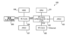
ここで、図22は従来の画像処理システムのコントローラ構成の一例を示すブロック図である。図22に示すように、画像処理システムのコントローラ100は、各デバイス間の画像データの入出力系の相互接続に関して、各デバイス間を同時に流れる大量のデータを絶え間なく管理するとともに、スキャナやプリンタなどの画像入出力装置200の機能を果たすよう、各デバイスを制御する。そして、高速処理が要求される場合には、CPU(Central Processing Unit)101やメインメモリ102などの高速化、大量の計算を必要とするアプリケーション、コネクティビティ(接続性)の向上などに適応すべく、画像データや制御コマンドなどの種々のデータの流れの速度(内部バンド幅)も高速化していく必要がある。しかし、パラレル方式のPCIバスでは、レーシングやスキューなどの問題がある。より具体的には、MCH(メモリコントロールハブ)と同様の機能を持つデバイス103は、CPU101からのメモリアクセスが発生した場合に、ポート1やポート2からのアクセスを拒否することがあり、その場合、デバイス104とデバイス105の間の画像データやその他のデータ転送を妨げられ、例えばHDD106やメモリ10a7からネットワークへの画像データ転送が滞ることがあった。一方、ポート1やポート2からのアクセスを拒否しない場合、CPU101の処理が妨げられるという問題があった。
Here, FIG. 22 is a block diagram showing an example of a controller configuration of a conventional image processing system. As shown in FIG. 22, the
最近では、パラレル方式のインタフェースに代えて、IEEE1394やUSB等の高速シリアルインタフェースの使用が検討されている。例えば、特許文献1によれば、内部インタフェースとして、IEEE1394やUSB等の高速シリアルインタフェースを使用することが提案されている。 Recently, the use of a high-speed serial interface such as IEEE1394 or USB is being considered in place of the parallel interface. For example, according to Patent Document 1, it is proposed to use a high-speed serial interface such as IEEE1394 or USB as an internal interface.
また、他の高速シリアルインタフェースとして、PCIバス方式の後継規格に当るPCI Express(登録商標)なるインタフェースも提案され、実用化の段階にきている(例えば、非特許文献1参照)。このPCI Expressシステムは、概略的には、例えば非特許文献1中の図1等に示されるようなルートコンプレックス−スイッチ(任意階層)−デバイス等のツリー構造(木構造)によるデータ通信網として構成されている。 As another high-speed serial interface, an interface called PCI Express (registered trademark), which is a successor to the PCI bus system, has been proposed and has been put to practical use (for example, see Non-Patent Document 1). This PCI Express system is schematically configured as a data communication network having a tree structure (tree structure) such as a root complex-switch (arbitrary hierarchy) -device as shown in FIG. Has been.
そして、特許文献2によれば、内部インタフェースとして、PCI Expressを使用することが提案されている。 According to Patent Document 2, it is proposed to use PCI Express as an internal interface.
ところが、特許文献2において提案されているような内部インタフェースとしてPCI Expressを使用する場合であっても、解決しなくてはならない問題がある。 However, even when PCI Express is used as an internal interface as proposed in Patent Document 2, there is a problem that must be solved.
例えば、図23に示すようなコントローラ300の構成である場合、デバイス301においてCPU302からメインメモリ303へのメモリアクセスが発生した場合には、デバイス304とデバイス305の間の画像データやその他のデータ転送が妨げられてしまうという問題がある。
For example, in the configuration of the
本発明は、上記に鑑みてなされたものであって、デバイス間の画像データやその他のデータ転送を妨げることのない制御装置、画像処理システムおよびデータ転送経路切替方法を提供することを目的とする。 The present invention has been made in view of the above, and an object thereof is to provide a control device, an image processing system, and a data transfer path switching method that do not hinder image data and other data transfer between devices. .
上述した課題を解決し、目的を達成するために、請求項1にかかる発明の制御装置は、プロセッサおよびメモリに接続されルート機能を有するルートデバイスと、前記ルートデバイスに第1のバスを介して接続される第1のデバイスと、前記ルートデバイスに第2のバスを介して接続されるとともに、前記第1のデバイスに第3のバスを介して接続される第2のデバイスと、を備え、前記ルートデバイスは、前記プロセッサが当該ルートデバイスを介して前記メモリにアクセスした場合に、前記第1のデバイスと前記ルートデバイスとを接続する前記第1のバスおよび前記ルートデバイスと前記第2のデバイスとを接続する前記第2のバスを経由する第1のデータ転送経路から前記第1のデバイスと前記第2のデバイスとを接続する前記第3のバスを経由する第2のデータ転送経路に切り替える切替手段を有する。 In order to solve the above-described problems and achieve the object, a control device according to a first aspect of the present invention includes a root device connected to a processor and a memory and having a root function, and the root device via a first bus. A first device to be connected; and a second device connected to the root device via a second bus and connected to the first device via a third bus; The root device includes the first bus and the root device and the second device that connect the first device and the root device when the processor accesses the memory via the root device. the third connecting the first from said data transfer path between the first device of the second device via the second bus connecting bets A switching means for switching to a second data transfer path via the bus.
また、請求項2にかかる発明は、請求項1記載の制御装置において、前記第1のデバイスおよび前記第2のデバイスは、前記第1のデータ転送経路から前記第2のデータ転送経路に切り替えるためのスイッチを夫々有するデバイスであり、前記切替手段は、前記第1のデータ転送経路から前記第2のデータ転送経路に切り替える制御を前記スイッチに行わせるための信号を前記第1のバスを介して前記第1のデバイスに送信するとともに前記第2のバスを介して前記第2のデバイスに送信することで、前記第1のデータ転送経路から前記第2のデータ転送経路に切り替える。 According to a second aspect of the present invention, in the control device according to the first aspect, the first device and the second device are switched from the first data transfer path to the second data transfer path. Each of the switches, and the switching means sends a signal for causing the switch to perform control to switch from the first data transfer path to the second data transfer path via the first bus. By transmitting to the first device and transmitting to the second device via the second bus, the first data transfer path is switched to the second data transfer path .
また、請求項3にかかる発明は、請求項1記載の制御装置において、前記第1のデバイスおよび前記第2のデバイスは、前記第1のデータ転送経路から前記第2のデータ転送経路に切り替えるためのスイッチを夫々有するデバイスであり、前記切替手段は、前記第1のデータ転送経路から前記第2のデータ転送経路に切り替える制御を前記スイッチに行わせるための前記第1のデバイスを通信先として示す通信アドレスを前記第2のデバイスに送信するとともに前記第2のデバイスを通信先として示す通信アドレスを前記第1のデバイスに送信することで、前記第1のデータ転送経路から前記第2のデータ転送経路に切り替える。 The invention according to claim 3 is the control device according to claim 1, wherein the first device and the second device are switched from the first data transfer path to the second data transfer path. And the switching means indicates the first device for causing the switch to perform control to switch from the first data transfer path to the second data transfer path as a communication destination. By transmitting a communication address to the second device and transmitting a communication address indicating the second device as a communication destination to the first device, the second data transfer from the first data transfer path Switch to a route .
また、請求項4にかかる発明は、請求項1記載の制御装置において、前記第1のデバイスおよび前記第2のデバイスは、前記第1のデータ転送経路から前記第2のデータ転送経路に切り替えるためのスイッチを夫々有するデバイスであり、前記ルートデバイスと前記第1のデバイスとを接続する前記第1のバスとは異なる第1の信号線をさらに具備し、前記ルートデバイスと前記第2のデバイスとを接続する前記第2のバスとは異なる第2の信号線をさらに具備し、前記切替手段は、前記第1のデータ転送経路から前記第2のデータ転送経路に切り替える制御を前記スイッチに行わせるための信号を前記第1の信号線を介して前記第1のデバイスに送信するとともに前記第2の信号線を介して前記第2のデバイスに送信することで、前記第1のデータ転送経路から前記第2のデータ転送経路に切り替える。 According to a fourth aspect of the present invention, in the control device according to the first aspect, the first device and the second device are switched from the first data transfer path to the second data transfer path. Each of the switches, further comprising a first signal line different from the first bus for connecting the root device and the first device, and the root device and the second device, further comprising a different second signal line and the second bus for connecting said switching means to perform the control of switching from the first data transfer path to said second data transfer path to the switch A signal for transmitting to the first device via the first signal line and to the second device via the second signal line. Switch from the data transfer path to said second data transfer path.
また、請求項5にかかる発明の画像処理システムは、プロセッサおよびメモリに接続されルート機能を有するとともに前記メモリに対する制御機能を有するメモリ制御デバイスと、前記メモリ制御デバイスに第1のバスを介して接続され、画像処理を実行する画像処理コントローラと、前記メモリ制御デバイスに第2のバスを介して接続されるとともに前記画像処理コントローラに第3のバスを介して接続され、I/Oデバイスを制御するI/O制御デバイスと、を備え、前記メモリ制御デバイスは、前記プロセッサが当該メモリ制御デバイスを介して前記メモリにアクセスした場合に、前記画像処理コントローラと前記I/O制御デバイスとの間に位置する前記第1のバスと前記メモリ制御デバイスとを接続する前記第1のバスおよび前記メモリ制御デバイスと前記I/O制御デバイスとを接続する前記第2のバスを経由する第1のデータ転送経路から前記画像処理コントローラと前記I/O制御デバイスとを接続する前記第3のバスを経由する第2のデータ転送経路に切り替える切替手段を有する。 According to a fifth aspect of the present invention, there is provided an image processing system connected to a processor and a memory, having a root function and having a control function for the memory, and being connected to the memory control device via a first bus. And an image processing controller that executes image processing and is connected to the memory control device via a second bus and to the image processing controller via a third bus to control the I / O device. An I / O control device, wherein the memory control device is positioned between the image processing controller and the I / O control device when the processor accesses the memory via the memory control device. It said first bus and said that the first bus to connect the memory control device Said third bus connecting the first data transfer path through the second bus for connecting the memory control device and the I / O control device and the image processing controller and said I / O control device There is a switching means for switching to the second data transfer path through.
また、請求項6にかかる発明は、請求項5記載の画像処理システムにおいて、 前記画像処理コントローラおよび前記I/O制御デバイスは、前記第1のデータ転送経路から前記第2のデータ転送経路に切り替えるためのスイッチを夫々有し、前記切替手段は、前記第1のデータ転送経路から前記第2のデータ転送経路に切り替える制御を前記スイッチに行わせるための信号を前記第1のバスを介して前記画像処理コントローラに送信するとともに前記第2のバスを介して前記I/O制御デバイスに送信することで、前記第1のデータ転送経路から前記第2のデータ転送経路に切り替える。 According to a sixth aspect of the present invention, in the image processing system according to the fifth aspect , the image processing controller and the I / O control device are switched from the first data transfer path to the second data transfer path. A switch for switching the switching means from the first data transfer path to the second data transfer path via the first bus. By transmitting to the image processing controller and transmitting to the I / O control device via the second bus, the first data transfer path is switched to the second data transfer path .
また、請求項7にかかる発明は、請求項5記載の画像処理システムにおいて、前記画像処理コントローラおよび前記I/Oデバイスは、前記第1のデータ転送経路から前記第2のデータ転送経路に切り替えるためのスイッチを夫々有し、前記切替段は、前記第1のデータ転送経路から前記第2のデータ転送経路に切り替える制御を前記スイッチに行わせるための前記画像処理コントローラを通信先として示す通信アドレスを前記I/O制御デバイスに送信するとともに前記I/O制御デバイスを通信先として示す通信アドレスを前記画像処理コントローラに送信することで、前記第1のデータ転送経路から前記第2のデータ転送経路に切り替える。
The invention according to
また、請求項8にかかる発明は、請求項5記載の画像処理システムにおいて、前記ルートデバイスと前記画像処理システムとを接続する前記第1のバスとは異なる第1の信号線をさらに具備し、前記ルートデバイスと前記I/O制御デバイスとを接続する前記第2のバスとは異なる第2の信号線をさらに具備し、前記切替手段は、前記第1のデータ転送経路から前記第2のデータ転送経路に切り替える制御を前記スイッチに行わせるための信号を前記第1の信号線を介して前記画像処理コントローラに送信するとともに前記第2の信号線を介して前記I/O制御デバイスに送信することで、前記第1のデータ転送経路から前記第2のデータ転送経路に切り替える。
The invention according to
また、請求項9にかかる発明のデータ転送経路切替方法は、プロセッサおよびメモリに接続されルート機能を有するルートデバイスによって実行されるデータ転送経路切替方法において、前記プロセッサが当該ルートデバイスを介して前記メモリにアクセスし、前記プロセッサによる前記メモリへのアクセスが発生した場合に、前記ルートデバイスに第1のバスを介して接続される第1のデバイスと前記ルートデバイスとを接続する前記第1のバスおよび前記ルートデバイスと前記ルートデバイスに第2のバスを介して接続されるとともに前記第1のデバイスに第3のバスを介して接続される第2のデバイスとを接続する前記第2のバスを経由する第1のデータ転送経路から前記第1のデバイスと前記第2のデバイスとを接続する前記第3のバスを経由する第2のデータ転送経路に切り替える。 A data transfer path switching method according to a ninth aspect of the present invention is the data transfer path switching method executed by a root device connected to the processor and the memory and having a root function. accessing, when access to the memory by the processor is generated, the first bus connecting the first device connected via the first bus to the root device and the said root device and via said second bus connecting the second device connected via a third bus to the first device is connected via a second bus to the root device and the root device first from the data transfer path said first device and the third for connecting the second device to Switch to the second data transfer path through the scan.
また、請求項10にかかる発明は、請求項9記載のデータ転送経路切替方法において、前記第1のデバイスおよび前記第2のデバイスは、前記第1のデータ転送経路から前記第2のデータ転送経路に切り替えるためのスイッチを夫々具備するデバイスであり、前記第1のデータ転送経路から前記第2のデータ転送経路に切り替える制御を前記スイッチに行わせるための信号を前記第1のバスを介して前記第1のデバイスに送信するとともに前記第2のバスを介して前記第2のデバイスに送信することで、前記第1のデータ転送経路から前記第2のデータ転送経路に切り替える。
The invention according to claim 10 is the data transfer path switching method according to
また、請求項11にかかる発明は、請求項9記載のデータ転送経路切替方法において、前記第1のデバイスおよび前記第2のデバイスは、前記第1のデータ転送経路から前記第2のデータ転送経路に切り替えるためのスイッチを夫々具備するデバイスであり、前記第1のデータ転送経路から前記第2のデータ転送経路に切り替える制御を前記スイッチに行わせるための前記第1のデバイスを通信先として示す通信アドレスを前記第2のデバイスに送信するとともに前記第2のデバイスを通信先として示す通信アドレスを前記第1のデバイスに送信することで、前記第1のデータ転送経路から前記第2のデータ転送経路に切り替える。
The invention according to claim 11 is the data transfer path switching method according to
また、請求項12にかかる発明は、請求項9記載のデータ転送経路切替方法において、前記第1のデバイスおよび前記第2のデバイスは、前記第1のデータ転送経路から前記第2のデータ転送経路に切り替えるためのスイッチを夫々有するデバイスであり、前記第1のデータ転送経路から前記第2のデータ転送経路に切り替える制御を前記スイッチに行わせるための信号を前記ルートデバイスと前記第1のデバイスとを接続する前記第1のバスとは異なる第1の信号線を介して前記第1のデバイスに送信するとともに前記ルートデバイスと前記第2のデバイスとを接続する前記第2のバスとは異なる第2の信号線を介して前記第2のデバイスに送信することで、前記第1のデータ転送経路から前記第2のデータ転送経路に切り替える。
The invention according to claim 12 is the data transfer path switching method according to
請求項1,5,9にかかる発明によれば、ルートデバイスにおいてCPUからのメモリアクセスが発生した場合にも、第1のデバイスと第2のデバイスを第2の高速シリアルバスにより直接接続したデータ転送経路を経由してデータ転送することにより、第1のデバイスと第2のデバイスの間の画像データやその他のデータ転送を妨げることのない制御装置を提供することができるという効果を奏する。 Claim 1, according to the invention of 5,9, even when the memory access from the CPU occurs in root device, and the first and second devices directly connected by a second high-speed serial bus data By transferring data via the transfer path, it is possible to provide a control device that does not hinder image data and other data transfer between the first device and the second device.
また、請求項2,6,10にかかる発明によれば、ルートデバイスからの信号に応じてデータ転送経路を切り替えることができるという効果を奏する。
Further, according to the inventions according to
また、請求項3,7,11にかかる発明によれば、パケットの通信先アドレスに応じてデータ転送経路を切り替えることができるという効果を奏する。 Further, according to the third , seventh , and eleventh aspects , the data transfer path can be switched according to the communication destination address of the packet.
また、請求項4,8,12にかかる発明によれば、信号線を経由してルートデバイスで発生した信号を第1のデバイスと第2のデバイスとに送信するようにしたことにより、データ転送経路の切り替え信号を高速に伝達することができるとともに、ルートデバイスからの信号に応じてデータ転送経路を切り替えることができる。
According to the inventions of
以下に添付図面を参照して、この発明にかかる制御装置、画像処理システムおよびデータ転送方法の最良な実施の形態を詳細に説明する。 Exemplary embodiments of a control device, an image processing system, and a data transfer method according to the present invention are explained in detail below with reference to the accompanying drawings.
[第1の実施の形態]
本発明の第1の実施の形態を図1ないし図17に基づいて説明する。以下では、PCI Expressの詳細について、[PCI Express規格の概要]〜[PCI Express のアーキテクチャの詳細]の欄で説明し、その後、本実施の形態の画像処理システムについて、[画像処理システム]の欄で説明する。
[First Embodiment]
A first embodiment of the present invention will be described with reference to FIGS. In the following, details of PCI Express will be described in the columns [Outline of PCI Express Standard] to [Details of Architecture of PCI Express], and then the [Image Processing System] column for the image processing system of the present embodiment. I will explain it.
[PCI Express規格の概要]
まず、本実施の形態は高速シリアルバスの一つであるPCI Express(登録商標)を利用するものであり、本実施の形態の前提として当該PCI Express規格の概要について、非特許文献1の一部抜粋により説明する。ここに、高速シリアルバスとは、1本の伝送路を用いてシリアル(直列)伝送により高速(100Mbps程度以上)にデータをやり取りすることができるインタフェースを意味する。
[Outline of PCI Express standard]
First, this embodiment uses PCI Express (registered trademark), which is one of high-speed serial buses. As an assumption of this embodiment, an outline of the PCI Express standard is a part of Non-Patent Document 1. Explained with excerpts. Here, the high-speed serial bus means an interface capable of exchanging data at high speed (about 100 Mbps or more) by serial (serial) transmission using a single transmission line.
PCI Expressは、PCIの後継規格としてコンピュータ全般に通用する標準拡張バスとして規格化されたバスであり、概略的には、低電圧差動信号伝送、ポイントツーポイントで送受信独立の通信チャネル、パケット化されたスプリットトランザクション、リンク構成の違いによる高いスケーラビリティなどの特徴を持つ。 PCI Express is a standardized expansion bus that can be used for all computers as a successor to PCI. In general, low-voltage differential signal transmission, point-to-point independent communication channels, and packetization Split transactions and high scalability due to differences in link configuration.
図1に既存のPCIシステム、図2にPCI Expressシステムの各々の構成例を示す。既存のPCIシステムにあっては、CPU100やAGPグラフィックス101やメモリ102が接続されたホストブリッジ103に対して、PCI-X(PCIの上位互換規格)デバイス104a,104bがPCI-Xブリッジ105aを介して接続されたり、PCIデバイス104c,104dが接続されたPCIブリッジ105bやPCIバススロット106が接続されたPCIブリッジ107がPCIブリッジ105cを介して接続されたりしたツリー構造(木構造)とされている。
FIG. 1 shows a configuration example of an existing PCI system, and FIG. 2 shows a configuration example of a PCI Express system. In the existing PCI system, PCI-X (PCI upward compatible standard)
これに対して、PCI Expressシステムにあっては、CPU110やメモリ111が接続されたルートコンプレックス112に対して、PCI Expressグラフィックス113がPCI Express114aにより接続され、また、エンドポイント115aやレガシーエンドポイント116aがPCI Express114bにより接続されたスイッチ117aがPCI Express114cにより接続され、さらには、エンドポイント115bやレガシーエンドポイント116bがPCI Express114dにより接続されたスイッチ117bやPCIバススロット118が接続されたPCIブリッジ119がPCI Express114eにより接続されたスイッチ117cがPCI Express114fにより接続されたツリー構造(木構造)とされている。
On the other hand, in the PCI Express system, the
実際に想定されるPCI Expressプラットホーム例を図3に示す。図示例は、デスクトップ/モバイルへの適用例を示し、CPU121がCPUホストバス122により接続され、メモリ123が接続されたメモリハブ124(ルートコンプレックスに相当する)に対して、例えば、グラフィックス125がx16のPCI Express126aにより接続され、また、変換機能を有するI/Oハブ127がPCI Express126bにより接続されている。このI/Oハブ127には、例えば、Serial ATA128によりストレージ129が接続され、LPC130によりローカルI/O131が接続され、USB 2.0132やPCIバススロット133が接続されている。さらには、I/Oハブ127には、PCI Express126cによりスイッチ134が接続され、このスイッチ134には、各々、PCI Express126d,126e,126fによりモバイルドック135、ギガビットイーサネット136(イーサネットは登録商標)、アドインカード137が接続されている。
An example of an actually assumed PCI Express platform is shown in FIG. The illustrated example shows an application example to desktop / mobile. For example,
即ち、PCI Expressシステムでは、従来のPCI,PCI-X,AGPといったバスがPCI Expressで置き換わり、既存のPCI/PCI-Xデバイスを接続するためにブリッジが使用される。チップセット間の接続もPCI Express接続となり、IEEE1394,Serial ATA,USB 2.0などの既存のバスはI/OハブによりPCI Expressに接続される。 That is, in the PCI Express system, the conventional PCI, PCI-X, AGP bus is replaced with PCI Express, and a bridge is used to connect an existing PCI / PCI-X device. Connection between chipsets is also PCI Express connection, and existing buses such as IEEE1394, Serial ATA, and USB 2.0 are connected to PCI Express by an I / O hub.
[PCI Expressの構成要素]
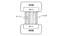
A.ポート(Port)/レーン(Lane)/リンク(Link)
図4に物理層の構造を示す。ポートは、物理的には同一半導体内にあり、リンクを形成するトランスミッタ/レシーバの集合で、論理的にはコンポーネント・リンク間を1対1で接続(ポイント・ツー・ポイント)するインタフェースを意味する。転送レートは、例えば片方向2.5Gbpsとされている。レーンは、例えば0.8Vの差動信号ペアのセットで、送信側の信号ペア(2本)、受信側の信号ペア(2本)からなる。リンクは、2つのポートとその間を結ぶレーンの集まりであり、コンポーネント間のデュアルシンプレックス通信バスである。「xNリンク」はN本のレーンから構成され、現在の規格では、N=1,2,4,8,16,32が定義されている。図示例は、x4リンク例である。例えば、図5に示すように、デバイスA,B間を結ぶこのレーン幅Nを可変することにより、スケーラブルなバンド幅を構成することが可能となる。
[Components of PCI Express]
A. Port / Lane / Link
FIG. 4 shows the structure of the physical layer. A port is a set of transmitters / receivers that are physically in the same semiconductor and form a link, and logically means an interface that connects component links in a one-to-one relationship (point-to-point). . The transfer rate is, for example, 2.5 Gbps in one direction. The lane is, for example, a set of 0.8 V differential signal pairs, and includes a transmission-side signal pair (two) and a reception-side signal pair (two). A link is a collection of lanes connecting two ports and the two ports, and is a dual simplex communication bus between components. The “xN link” is composed of N lanes, and N = 1, 2, 4, 8, 16, 32 are defined in the current standard. The illustrated example is an x4 link example. For example, as shown in FIG. 5, by changing the lane width N connecting the devices A and B, a scalable bandwidth can be configured.
B.ルートコンプレックス(Root Complex)
ルートコンプレックス112は、I/O構造の最上位に位置し、CPUやメモリサブシステムをI/Oに接続する。ブロック図などでは、図3に示すように、「メモリハブ」と記述されることが多い。ルートコンプレックス112(又は、124)は、1つ以上のPCI Expressポート(ルートポート)(図2中では、ルートコンプレックス112中の四角で示す)を持ち、各々のポートは独立したI/O階層ドメインを形成する。I/O階層ドメインは、単純なエンドポイントである場合(例えば、図2中のエンドポイント115a側の例)や、多数のスイッチやエンドポイントから形成される場合(例えば、図2中のエンドポイント115bやスイッチ117b,115c側の例)がある。
B. Root Complex
The
C.エンドポイント(End Point)
エンドポイント115は、タイプ00hのコンフィグレーション空間ヘッダを持つデバイス(具体的には、ブリッジ以外のデバイス)で、レガシーエンドポイントとPCI Expressエンドポイントとに分けられる。両者の大きな違いは、PCI ExpressエンドポイントはBAR(ベースアドレスレジスタ)でI/Oリソースを要求せず、このためI/Oリクエストを要求しない。また、PCI Expressエンドポイントは、ロックリクエストもサポートしていない。
C. End point
The endpoint 115 is a device having a configuration space header of type 00h (specifically, a device other than a bridge), and is divided into a legacy endpoint and a PCI Express endpoint. The major difference between the two is that the PCI Express endpoint does not request I / O resources in the BAR (Base Address Register), and therefore does not request an I / O request. PCI Express endpoints also do not support lock requests.
D.スイッチ(Switch)
スイッチ117(又は、134)は、2つ以上のポートを結合し、ポート間でのパケットルーティングを行う。コンフィグレーションソフトウェアからは、当該スイッチは、図6に示すように、仮想PCI-PCIブリッジ141の集合体として認識される。図中、両矢印はPCI Expressリンク114(又は、126)を示し、142a〜142dはポートを示す。このうち、ポート142aはルートコンプレックスに近い方のアップストリームポートであり、ポート142b〜142dはルートコンプレックスから遠い方のダウンストリームポートである。
D. Switch
The switch 117 (or 134) couples two or more ports and performs packet routing between the ports. From the configuration software, the switch is recognized as a collection of virtual PCI-PCI bridges 141 as shown in FIG. In the figure, double-headed arrows indicate PCI Express links 114 (or 126), and 142a to 142d indicate ports. Of these, the
E.PCI Express114e−PCIブリッジ119
PCI ExpressからPCI/PCI-Xへの接続を提供する。これにより、既存のPCI/PCI-XデバイスをPCI Expressシステム上で使用することができる。
Provides connection from PCI Express to PCI / PCI-X. Thereby, an existing PCI / PCI-X device can be used on the PCI Express system.
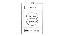
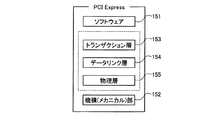
[階層アーキテクチャ]
従来のPCIのアーキテクチャは、図7−1に示すように、プロトコルとシグナリングが密接に関連する構造であり階層という考え方はなかったが、PCI Expressでは、図7−2に示すように、一般的な通信プロトコルやInfiniBandのように、独立した階層構造とされ、各層に分けて仕様が定義されている。即ち、最上位のソフトウェア151、最下位の機構(メカニカル)部152間に、トランザクション層153、データリンク層154、物理層155を持つ構造とされている。これにより、各層のモジュール性が確保され、スケーラビリティを持たせることやモジュールの再利用が可能となる。例えば、新たな信号コーディング方式や伝送媒体を採用する場合、物理層を変更するだけでデータリンク層やトランザクション層は変更せずに対応できる。
[Hierarchical architecture]
As shown in FIG. 7A, the conventional PCI architecture has a structure in which protocols and signaling are closely related and there is no concept of hierarchy. In PCI Express, as shown in FIG. Like the standard communication protocol and InfiniBand, it has an independent hierarchical structure, and specifications are defined for each layer. In other words, a
PCI Expressのアーキテクチャの中心となるのは、トランザクション層153、データリンク層154、物理層155であり、各々図8を参照して説明する以下のような役割を持つ。
The core of the PCI Express architecture is a
A.トランザクション層153
トランザクション層153は、最上位に位置し、トランザクションレイヤパケット(TLP)の組み立て、分解機能を持つ。トランザクションレイヤパケット(TLP)は、リード/ライト、各種イベントといったトランザクションの伝達に用いられる。また、トランザクション層153は、トランザクションレイヤパケット(TLP)のためのクレジットを用いたフロー制御を行う。各層153〜155におけるトランザクションレイヤパケット(TLP)の概要を図9に示す(詳細は、後述する)。
The
B.データリンク層154
データリンク層154の主な役割は、エラー検出/訂正(再送)によりトランザクションレイヤパケット(TLP)のデータ完全性を保証することと、リンク管理である。データリンク層154間では、リンク管理やフロー制御のためのパケットのやり取りを行う。このパケットは、トランザクションレイヤパケット(TLP)と区別するために、データリンクレイヤパケット(DLLP)と呼ばれる。
B.
The main role of the
C.物理層155
物理層155は、ドライバ、入力バッファ、パラレル−シリアル/シリアル−パラレル変換器、PLL、インピーダンス整合回路といったインタフェース動作に必要な回路を含んでいる。また、論理的な機能としてインタフェースの初期化・保守の機能を持つ。物理層155は、データリンク層154/トランザクション層153を実際のリンクで使用される信号技術から独立させる役目も持っている。
The
なお、PCI Expressのハードウェア構成上、エンベデッド・クロックという技術を採用しており、クロック信号はなく、クロックのタイミングはデータ信号中に埋め込まれており、受信側でデータ信号のクロス・ポイントを基にクロックを抽出する方式とされている。 The PCI Express hardware configuration employs a technology called embedded clock, there is no clock signal, the clock timing is embedded in the data signal, and the receiving side is based on the cross-point of the data signal. The system extracts the clock.
[コンフィグレーション空間]
PCI Expressは、従来のPCIと同様にコンフィグレーション空間を持つが、その大きさは従来のPCIが256バイトであるのに対して、図10に示すように、4096バイトへと拡張されている。これにより、多数のデバイス固有レジスタセットを必要とするデバイス(ホストブリッジなど)に対しても、将来的に十分な空間が確保されている。PCI Expressでは、コンフィグレーション空間へのアクセスは、フラットなメモリ空間へのアクセス(コンフィグレーションリード/ライト)で行われ、バス/デバイス/機能/レジスタ番号はメモリアドレスにマップされている。
[Configuration space]
PCI Express has a configuration space like conventional PCI, but its size is expanded to 4096 bytes as shown in FIG. 10, whereas conventional PCI has 256 bytes. As a result, sufficient space is secured in the future even for devices (such as host bridges) that require a large number of device-specific register sets. In PCI Express, the configuration space is accessed by accessing a flat memory space (configuration read / write), and the bus / device / function / register number is mapped to a memory address.
当該空間の先頭256バイトは、PCIコンフィグレーション空間として、BIOSや従来のOSからI/Oポートを使用した方法でもアクセスできる。従来のアクセスをPCI Expressでのアクセスに変換する機能は、ホストブリッジ上に実装される。00hから3FhまではPCI2.3互換のコンフィグレーションヘッダとなっている。これにより、PCI Expressで拡張された機能以外であれば、従来のOSやソフトウェアをそのまま使用することができる。即ち、PCI Expressにおけるソフトウェア層は、既存のPCIと互換性を保ったロード・ストア・アーキテクチャ(プロセッサが直接I/Oレジスタをアクセスする方式)を継承している。しかし、PCI Expressで拡張された機能(例えば、同期転送やRAS(Reliability,Availability and Serviceability)などの機能)を使用するには、4KバイトのPCI Express拡張空間にアクセスできるようにする必要がある。 The first 256 bytes of the space can be accessed as a PCI configuration space by a method using an I / O port from a BIOS or a conventional OS. The function of converting conventional access to PCI Express access is implemented on the host bridge. From 00h to 3Fh, it is a PCI2.3 compatible configuration header. As a result, a conventional OS and software can be used as they are except for functions extended by PCI Express. That is, the software layer in PCI Express inherits a load / store architecture (a method in which a processor directly accesses an I / O register) that is compatible with the existing PCI. However, in order to use functions expanded by PCI Express (for example, functions such as synchronous transfer and RAS (Reliability, Availability and Serviceability)), it is necessary to make it possible to access a 4 Kbyte PCI Express expansion space.
なお、PCI Expressとしては様々なフォームファクタ(形状)が考えられるが、具体化している例としては、アドインカード、プラグインカード(Express Card)、Mini PCI Expressなどがある。 Various form factors (shapes) are conceivable as PCI Express. Examples of specific examples include add-in cards, plug-in cards (Express Cards), and Mini PCI Express.
[PCI Express のアーキテクチャの詳細]
PCI Express のアーキテクチャの中心となっているトランザクション層153、データリンク層154、物理層155について、各々詳細に説明する。
[PCI Express architecture details]
The
A.トランザクション層153
トランザクション層153の主な役割は、前述したように、上位のソフトウェア層151と下位のデータリンク層154との間でトランザクションレイヤパケット(TLP)の組み立てと分解を行うことである。
The main role of the
a.アドレス空間とトランザクションタイプ
PCI Expressでは、従来のPCIでサポートされていたメモリ空間(メモリ空間とのデータ転送用)、I/O空間(I/O空間とのデータ転送用)、コンフィグレーション空間(デバイスのコンフィグレーションとセットアップ用)に加えて、メッセージ空間(PCI Expressデバイス間のインバンドでのイベント通知や一般的なメッセージ送信(交換)用…割り込み要求や確認は、メッセージを「仮想ワイヤ」として使用することにより伝達される)が追加され、4つのアドレス空間が定義されている。各々の空間に対してトランザクションタイプが定義されている(メモリ空間、I/O空間、コンフィグレーション空間は、リード/ライト、メッセージ空間は基本(ベンダ定義含む))。
a. Address space and transaction type
In PCI Express, memory space (for data transfer with memory space), I / O space (for data transfer with I / O space), and configuration space (device configuration and setup) supported by conventional PCI In addition to message space (in-band event notification between PCI Express devices and general message transmission (exchange) ... Interrupt requests and confirmations are communicated by using the message as a "virtual wire" And four address spaces are defined. Transaction types are defined for each space (memory space, I / O space, configuration space is read / write, and message space is basic (including vendor definition)).
b.トランザクションレイヤパケット(TLP)
PCI Expressは、パケット単位で通信を行う。図9に示したトランザクションレイヤパケット(TLP)のフォーマットにおいて、ヘッダのヘッダ長は3DW(DWはダブルワードの略;合計12バイト)又は4DW(16バイト)で、トランザクションレイヤパケット(TLP)のフォーマット(ヘッダ長とペイロードの有無)、トランザクションタイプ、トラフィッククラス(TC)、アトリビュートやペイロード長などの情報が含まれる。パケット内の最大ペイロード長は1024DW(4096バイト)である。
b. Transaction layer packet (TLP)
PCI Express performs communication in units of packets. In the transaction layer packet (TLP) format shown in FIG. 9, the header length of the header is 3DW (DW is an abbreviation of double word; total 12 bytes) or 4DW (16 bytes), and the transaction layer packet (TLP) format ( Information such as header length and presence / absence of payload), transaction type, traffic class (TC), attribute, and payload length are included. The maximum payload length in the packet is 1024 DW (4096 bytes).
ECRCは、エンドツーエンドのデータ完全性を保証するためのもので、トランザクションレイヤパケット(TLP)部分の32ビットCRCである。これは、スイッチ内部などでトランザクションレイヤパケット(TLP)にエラーが発生した場合、LCRC(リンクCRC)ではエラーを検出できないためである(エラーとなったTLPでLCRCが再計算されるため)。 ECRC is an end-to-end data integrity guarantee and is a 32-bit CRC of the transaction layer packet (TLP) portion. This is because when an error occurs in the transaction layer packet (TLP) inside the switch or the like, the LCRC (link CRC) cannot detect the error (because the LCRC is recalculated with the TLP in error).
リクエストは、完了パケットが不要なものと必要なものとがある。 Some requests do not require a completion packet, and some requests.
c.トラフィッククラス(TC)と仮想チャネル(VC)
上位のソフトウェアは、トラフィッククラス(TC)を使用することによりトラフィックの差別化(優先度をつける)を行うことができる。例えば、映像データをネットワークのデータよりも優先して転送する、といったことが可能となる。トラフィッククラス(TC)はTC0からTC7まで8つある。
c. Traffic class (TC) and virtual channel (VC)
Upper software can differentiate (prioritize) traffic by using a traffic class (TC). For example, video data can be transferred with priority over network data. There are eight traffic classes (TC) from TC0 to TC7.
仮想チャネル(VC:Vertual Channel)は、各々独立した仮想通信バス(同一のリンクを共用する複数の独立したデータ・フロー・バッファを使用するメカニズム)で、各々がリソース(バッファやキュー)を持ち、図11に示すように、独立したフロー制御を行う。これにより、1つの仮想チャネルのバッファが満杯の状態(full)になっても、他の仮想チャネルの転送を行うことができる。つまり、物理的には1つのリンクを仮想的な複数のチャネルに分けることで、有効に使用することができる。例えば、図11中に示すように、スイッチを経由してルートのリンクが複数のデバイスに分かれる場合、各デバイスのトラフィックの優先度を制御することができる。VC0は必須で、コストパフォーマンスのトレードオフに応じてその他の仮想チャネル(VC1〜VC7)が実装される。図11中の実線矢印は、デフォルト仮想チャネル(VC0)を示し、破線矢印はその他の仮想チャネル(VC1〜VC7)を示している。 A virtual channel (VC) is an independent virtual communication bus (a mechanism that uses a plurality of independent data flow buffers sharing the same link), each having resources (buffers and queues) As shown in FIG. 11, independent flow control is performed. Thereby, even if the buffer of one virtual channel becomes full (full), the transfer of another virtual channel can be performed. In other words, it can be used effectively by physically dividing one link into a plurality of virtual channels. For example, as shown in FIG. 11, when a route link is divided into a plurality of devices via a switch, the priority of traffic of each device can be controlled. VC0 is indispensable, and other virtual channels (VC1 to VC7) are mounted in accordance with the cost performance trade-off. The solid line arrow in FIG. 11 indicates the default virtual channel (VC0), and the broken line arrow indicates the other virtual channels (VC1 to VC7).
トランザクション層内では、トラフィッククラス(TC)が仮想チャネル(VC)にマッピングされる。1つの仮想チャネル(VC)に対して1つ又は複数のトラフィッククラス(TC)をマッピングできる(仮想チャネル(VC)の数が少ない場合)。単純な例では、各トラフィッククラス(TC)から各仮想チャネル(VC)に1対1、全てのトラフィッククラス(TC)を仮想チャネルVC0にマッピングする、といったことが考えられる。TC0−VC0のマッピングは、必須/固定で、それ以外のマッピングは上位のソフトウェアから制御される。ソフトウェアはトラフィッククラス(TC)を利用することで、トランザクションの優先度を制御することが可能となる。 Within the transaction layer, a traffic class (TC) is mapped to a virtual channel (VC). One or more traffic classes (TC) can be mapped to one virtual channel (VC) (when the number of virtual channels (VC) is small). In a simple example, it can be considered that each traffic class (TC) is mapped to each virtual channel (VC) on a one-to-one basis, and all traffic classes (TC) are mapped to the virtual channel VC0. The mapping of TC0-VC0 is essential / fixed, and the other mappings are controlled from the upper software. The software can control the priority of the transaction by using the traffic class (TC).
d.フロー制御
受信バッファのオーバーフローを避け、伝送順序を確立するためにフロー制御(FC:Flow Control)が行われる。フロー制御は、リンク間のポイントツーポイントで行われ、エンドツーエンドではない。従って、フロー制御により最終的な相手(コンプリータ)にパケットが届いたことを確認することはできない。
d. Flow control Flow control (FC) is performed in order to avoid overflow of the reception buffer and establish the transmission order. Flow control is done point-to-point between links, not end-to-end. Therefore, it cannot be confirmed that the packet has reached the final partner (completer) by flow control.
PCI Expressのフロー制御は、クレジット・ベースで行われる(データ転送を始める前に、受け取り側のバッファの空き状況を確認し、オーバーフロー、アンダフローが発生しないメカニズム)。即ち、受信側はリンク初期化時にバッファ容量(クレジット値)を送信側に通知し、送信側はクレジット値と送信するパケットの長さとを比較し、一定の残りがある場合のみパケットを送信する。このクレジットには6種類ある。 PCI Express flow control is performed on a credit basis (mechanism to check the buffer availability on the receiving side before starting data transfer and prevent overflow and underflow). That is, the receiving side notifies the transmitting side of the buffer capacity (credit value) at the time of link initialization, and the transmitting side compares the credit value with the length of the packet to be transmitted, and transmits the packet only when there is a certain remaining. There are six types of credits.
フロー制御の情報交換はデータリンク層のデータリンクレイヤパケット(DLLP)を使用して行われる。フロー制御はトランザクションレイヤパケット(TLP)のみに適用され、データリンクレイヤパケット(DLLP)には適用されない(DLLPは常時送受信可能)。 Flow control information exchange is performed using data link layer packets (DLLP) in the data link layer. The flow control is applied only to the transaction layer packet (TLP) and not to the data link layer packet (DLLP) (DLLP can always be transmitted / received).
B.データリンク層154
データリンク層154の主な役割は、前述したように、リンク上の2つのコンポーネント間での信頼性の高いトランザクションレイヤパケット(TLP)交換機能を提供することである。
B.
The main role of the
a.トランザクションレイヤパケット(TLP)の扱い
トランザクション層153から受け取ったトランザクションレイヤパケット(TLP)に対しては、先頭に2バイトのシーケンス番号、末尾に4バイトのリンクCRC(LCRC)を付加して、物理層155に渡す(図9参照)。トランザクションレイヤパケット(TLP)は、リトライバッファに保管され、相手から受信確認(ACK)が届くまで再送される。トランザクションレイヤパケット(TLP)の送信に失敗が続いた場合は、リンク異常であると判断して物理層155に対してリンクの再トレーニングを要求する。リンクのトレーニングが失敗した場合、データリンク層154の状態はインアクティブに遷移する。
a. Handling of transaction layer packet (TLP) For the transaction layer packet (TLP) received from the
物理層155から受け取ったトランザクションレイヤパケット(TLP)は、シーケンス番号とリンクCRC(LCRC)が検査され、正常であればトランザクション層153に渡され、エラーがあった場合は再送を要求する。
The transaction layer packet (TLP) received from the
b.データリンクレイヤパケット(DLLP)
トランザクションレイヤパケット(TLP)は、物理層から送信されるときに自動的に図12に示すようなデータリンクレイヤパケット(DLLP)に分割されて各レーンに送信される。データリンク層154が生成するパケットは、データリンクレイヤパケット(DLLP)と呼ばれ、データリンク層154間でやり取りされる。データリンクレイヤパケット(DLLP)には、
・Ack/Nak:TLPの受信確認、リトライ(再送)
・InitFC1/InitFC2/UpdateFC:フロー制御の初期化とアップデート
・電源管理のためのDLLP
なる種類がある。
b. Data link layer packet (DLLP)
The transaction layer packet (TLP) is automatically divided into data link layer packets (DLLP) as shown in FIG. 12 and transmitted to each lane when transmitted from the physical layer. A packet generated by the
-Ack / Nak: TLP reception confirmation, retry (retransmission)
-InitFC1 / InitFC2 / UpdateFC: Flow control initialization and update-DLLLP for power management
There are different types.
図12に示すように、データリンクレイヤパケット(DLLP)の長さは6バイトで、種類を示すDLLPタイプ(1バイト)、DLLPの種類で固有の情報(3バイト)、CRC(2バイト)から構成される。 As shown in FIG. 12, the length of the data link layer packet (DLLP) is 6 bytes. From the DLLP type (1 byte) indicating the type, the information specific to the type of DLLP (3 bytes), and CRC (2 bytes) Composed.
C.物理層−論理サブブロック156
図8中に示す物理層155の論理サブブロック156での主な役割は、データリンク層154から受け取ったパケットを電気サブブロック157で送信できる形式に変換することである。また、物理層155を制御/管理する機能も有する。
C. Physical layer-
The main role of the
a.データ符号化とパラレル−シリアル変換
PCI Expressは、連続した“0”や“1”が続かないように(長い期間、クロス・ポイントが存在しない状態が続かないようにするため)、データ符号化に8B/10B変換を用いる。変換されたデータは、図13中に示すように、シリアル変換され、LSBからレーン上に送信される。ここに、レーンが複数ある場合は(図13はx4リンクの場合を例示している)、符号化の前にデータがバイト単位で各レーンに割り振られる。この場合、一見パラレル・バスのようにみえるが、レーン毎に独立した転送を行うので、パラレル・バスで問題となるスキューが大幅に緩和される。
a. Data encoding and parallel-serial conversion
PCI Express uses 8B / 10B conversion for data encoding so that consecutive “0” s and “1” s do not continue (in order not to maintain a state where there is no cross point for a long period of time). The converted data is serial-converted and transmitted from the LSB onto the lane as shown in FIG. Here, when there are a plurality of lanes (FIG. 13 illustrates the case of x4 link), data is allocated to each lane in units of bytes before encoding. In this case, it looks like a parallel bus at first glance, but since the transfer is performed independently for each lane, the skew which is a problem with the parallel bus is greatly reduced.
b.電源管理とリンクステート
リンクの消費電力を低く抑えるために、図14に示すように、L0/L0s/L1/L2というリンクステートが定義されている。
b. Power Management and Link State In order to keep the power consumption of the link low, a link state of L0 / L0s / L1 / L2 is defined as shown in FIG.
L0が通常モードで、L0sからL2へと低消費電力となるが、L0への復帰にも時間がかかるようになる。図15に示すように、ソフトウェアによる電源管理に加えて、アクティブステート電源管理を積極的に行うことにより、消費電力を極力小さくすることが可能となる。 L0 is a normal mode, and power consumption is reduced from L0s to L2, but it takes time to return to L0. As shown in FIG. 15, by actively performing active state power management in addition to software power management, it is possible to reduce power consumption as much as possible.
D.物理層−電気サブブロック157
物理層155の電気サブブロック157での主な役割は、論理サブブロック156でシリアル化されたデータをレーン上に送信することと、レーン上のデータを受信して論理サブブロック156に渡すことである。
D. Physical layer—
The main role of the
a.ACカップリング
リンクの送信側では、ACカップリング用のコンデンサが実装される。これにより、送信側と受信側のDCコモンモード電圧が同一である必要がなくなる。このため、送信側と受信側で異なる設計、半導体プロセス、電源電圧を使用することが可能となる。
a. AC coupling On the transmission side of the link, a capacitor for AC coupling is mounted. This eliminates the need for the DC common mode voltage on the transmission side and the reception side to be the same. For this reason, it is possible to use different designs, semiconductor processes, and power supply voltages on the transmission side and the reception side.
b.デエンファシス
PCI Expressでは、前述したように、8B/10Bエンコーディングによってできるだけ連続した“0”や“1”が続かないように処理されるが、連続した“0”や“1”が続くこともある(最大5回)。この場合、送信側はデエンファシス転送を行わなければならないことが規定されている。同一極性のビットが連続する場合は、2つ目のビットからは差動電圧レベル(振幅)を3.5±0.5dB落とすことで、受信側で受け取る信号のノイズ・マージンを稼ぐ必要がある。これを、デエンファシスという。伝送路の周波数依存性減衰のため、変化するビットの場合は高周波成分が多く、減衰により受信側の波形が小さくなるが、変化しないビットの場合は高周波成分が少なく、相対的に受信側の波形が大きくなる。このため、受信側での波形を一定とするためにデエンファシスを行う。
b. De-emphasis
In PCI Express, as described above, processing is performed so that continuous “0” and “1” do not continue as much as possible by 8B / 10B encoding, but continuous “0” and “1” may continue (maximum). 5 times). In this case, it is specified that the transmission side must perform de-emphasis transfer. When bits of the same polarity are consecutive, it is necessary to increase the noise margin of the signal received on the receiving side by dropping the differential voltage level (amplitude) from the second bit by 3.5 ± 0.5 dB. . This is called de-emphasis. Due to the frequency-dependent attenuation of the transmission line, there are many high-frequency components in the case of changing bits, and the waveform on the receiving side becomes small due to attenuation. Becomes larger. For this reason, de-emphasis is performed in order to make the waveform on the receiving side constant.
[画像処理システム]
本実施の形態のデジタル複写機やMFP等の画像処理システムは、その内部インタフェースに前述したようなPCI Express規格の高速シリアルバスを利用するようにしたものである。
[Image processing system]
The image processing system such as a digital copying machine or MFP according to the present embodiment uses a PCI Express standard high-speed serial bus as described above for its internal interface.
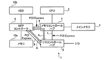
図16は、本実施の形態の画像処理システムの制御装置1の構成例を示す概略ブロック図である。本実施の形態の画像処理システムは、例えばMFP等の機器に適用されるもので、その制御装置1の構成要素として、システム全体の制御を受け持つCPU2と、メインメモリ3と、ルート機能を有するメモリ制御デバイスであるメモリコントロールハブ4と、第2のデバイスであってI/O制御デバイスであるI/Oコントロールハブ5と、第1のデバイスであってMFPにおける各種処理を制御する画像処理コントローラであるMFPコントローラ6と、メモリ10aと、HDD(Hard Disk Drive)10bとを備える。
FIG. 16 is a schematic block diagram illustrating a configuration example of the control device 1 of the image processing system according to the present embodiment. The image processing system according to the present embodiment is applied to a device such as an MFP, for example. As components of the control device 1, a CPU 2 that controls the entire system, a main memory 3, and a memory having a root function A
メモリコントロールハブ4は、PCI Express規格のルートコンプレックス(木構造のルート機能を有するデバイスであるルートデバイス)に相当するものであって、メインメモリ3を制御してCPU2やI/Oコントロールハブ5に接続されたI/Oデバイスとのデータ転送を司る。
The
I/Oコントロールハブ5は、接続されたI/Oデバイス(例えば、ハードディスクやグラフィックス、ネットワークなど)、またはそのインタフェースを制御する。
The I /
本実施の形態においては、メモリコントロールハブ4とI/Oコントロールハブ5との間、メモリコントロールハブ4とMFPコントローラ6との間は、それぞれPCI Express規格の高速シリアルバス7,8により接続されている。このように高速シリアルバス7,8により接続することにより、メモリコントロールハブ4を経由したI/Oコントロールハブ5からMFPコントローラ6に対するデータ転送(データ転送経路A)の高速化が図られている。
In this embodiment, the
加えて、本実施の形態においては、I/Oコントロールハブ5とMFPコントローラ6との間を、第2の高速シリアルバスであるPCI Express規格の高速シリアルバス9により接続している。すなわち、本実施の形態の画像処理システムの制御装置1は、メモリコントロールハブ4経由のデータ転送経路Aのほかに、I/Oコントロールハブ5とMFPコントローラ6とを直接接続したデータ転送経路Bを有している。
In addition, in this embodiment, the I /
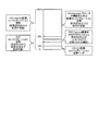
また、図17に示すように、MFPコントローラ6には、メモリコントロールハブ4からの信号1を受け、I/Oコントロールハブ5へのデータ転送経路をメモリコントロールハブ4経由のデータ転送経路AからI/Oコントロールハブ5とMFPコントローラ6とを直接接続したデータ転送経路Bへ切り替えるスイッチ11が備えられている。一方、I/Oコントロールハブ5には、メモリコントロールハブ4からの信号2を受け、MFPコントローラ6へのデータ転送経路をメモリコントロールハブ4経由のデータ転送経路AからI/Oコントロールハブ5とMFPコントローラ6とを直接接続したデータ転送経路Bへ切り替えるスイッチ12が備えられている。
As shown in FIG. 17, the
このような構成において、メモリコントロールハブ4からの信号1,2に応じたデータ転送経路の切り替え制御について説明する。
In such a configuration, data transfer path switching control according to signals 1 and 2 from the
メモリコントロールハブ4においてCPU2からのメモリアクセスが発生した場合、メモリコントロールハブ4からの信号1及び信号2によりMFPコントローラ6のスイッチ11とI/Oコントロールハブ5のスイッチ12とを制御し、MFPコントローラ6とI/Oコントロールハブ5を直接接続したデータ転送経路Bを経由して、MFPコントローラ6とI/Oコントロールハブ5の間でデータ転送を行うようにする。ここに、経路切替手段が実現されている。
When a memory access from the CPU 2 occurs in the
これにより、メモリコントロールハブ4においてCPU2からのメモリアクセスが発生した場合にも、MFPコントローラ6とI/Oコントロールハブ5を直接接続したデータ転送経路Bを経由してデータ転送することにより、MFPコントローラ6とI/Oコントロールハブ5の間の画像データやその他のデータ転送を妨げることのないデータ転送システムを提供することができる。
As a result, even when a memory access from the CPU 2 occurs in the
このように本実施の形態によれば、メモリコントロールハブ4においてCPU2からのメモリアクセスが発生した場合にも、MFPコントローラ6とI/Oコントロールハブ5を直接接続したデータ転送経路を経由してデータ転送することにより、MFPコントローラ6とI/Oコントロールハブ5の間の画像データやその他のデータ転送を妨げることのない画像処理システムを提供することができ、コントローラの同時並行動作を実現することができる。
As described above, according to the present embodiment, even when a memory access from the CPU 2 occurs in the
また、メモリコントロールハブ4からの信号に応じてデータ転送経路を切り替えることができる。
Further, the data transfer path can be switched in accordance with a signal from the
[第2の実施の形態]
次に、本発明の第2の実施の形態を図18に基づいて説明する。なお、前述した第1の実施の形態と同じ部分は同じ符号で示し説明も省略する。
[Second Embodiment]
Next, a second embodiment of the present invention will be described with reference to FIG. The same parts as those in the first embodiment described above are denoted by the same reference numerals, and description thereof is also omitted.
第1の実施の形態においては、メモリコントロールハブ4においてCPU2からのメモリアクセスが発生した場合、メモリコントロールハブ4からMFPコントローラ6とI/Oコントロールハブ5に対してPCI Express規格の高速シリアルバス7,8を経由して信号1,2をそれぞれ送信してデータ転送経路を切り替えるようにしたが、本実施の形態においては、通信先アドレスに従ってデータ転送経路を切り替えるようにしたものである。
In the first embodiment, when a memory access from the CPU 2 occurs in the
図18は、本発明の第2の実施の形態の画像処理システムの制御装置1の構成例を示す概略ブロック図である。図18に示すように、MFPコントローラ6には、通信先アドレスがI/Oコントロールハブ5の場合に、I/Oコントロールハブ5へのデータ転送経路をメモリコントロールハブ4経由のデータ転送経路AからI/Oコントロールハブ5とMFPコントローラ6とを直接接続したデータ転送経路Bへ切り替えるスイッチ21が備えられている。一方、I/Oコントロールハブ5には、通信先アドレスがMFPコントローラ6の場合に、MFPコントローラ6へのデータ転送経路をメモリコントロールハブ4経由のデータ転送経路AからI/Oコントロールハブ5とMFPコントローラ6とを直接接続したデータ転送経路Bへ切り替えるスイッチ22が備えられている。
FIG. 18 is a schematic block diagram illustrating a configuration example of the control device 1 of the image processing system according to the second embodiment of the present invention. As shown in FIG. 18, when the communication destination address is the I /
このような構成において、通信先アドレスに応じたデータ転送経路の切り替え制御について説明する。 In such a configuration, switching control of the data transfer path according to the communication destination address will be described.
本実施の形態においては、通信先アドレスによりMFPコントローラ6のスイッチ21とI/Oコントロールハブ5のスイッチ22とを制御し、MFPコントローラ6とI/Oコントロールハブ5を直接接続したデータ転送経路Bを経由して、MFPコントローラ6とI/Oコントロールハブ5の間でデータ転送を行うようにする。ここに、パケットの通信先アドレスによる経路切替手段が実現されている。
In this embodiment, the switch 21 of the
これにより、メモリコントロールハブ4においてCPU2からのメモリアクセスが発生した場合にも、MFPコントローラ6とI/Oコントロールハブ5を直接接続したデータ転送経路Bを経由してデータ転送することにより、MFPコントローラ6とI/Oコントロールハブ5の間の画像データやその他のデータ転送を妨げることのないデータ転送システムを提供することができる。
As a result, even when a memory access from the CPU 2 occurs in the
このように本実施の形態によれば、通信先アドレスに応じてデータ転送経路を切り替えることができる。 Thus, according to the present embodiment, the data transfer path can be switched according to the communication destination address.
[第3の実施の形態]
次に、本発明の第3の実施の形態を図19ないし図21に基づいて説明する。なお、前述した第1の実施の形態と同じ部分は同じ符号で示し説明も省略する。
[Third Embodiment]
Next, a third embodiment of the present invention will be described with reference to FIGS. The same parts as those in the first embodiment described above are denoted by the same reference numerals, and description thereof is also omitted.
第1の実施の形態においては、メモリコントロールハブ4においてCPU2からのメモリアクセスが発生した場合、メモリコントロールハブ4からMFPコントローラ6とI/Oコントロールハブ5に対してPCI Express規格の高速シリアルバス7,8を経由して信号1,2をそれぞれ送信してデータ転送経路を切り替えるようにしたが、本実施の形態においては、高速シリアルバス7,8とは別に信号線を設け、この信号線を経由して信号1,2をそれぞれ送信してデータ転送経路を切り替えるようにしたものである。
In the first embodiment, when a memory access from the CPU 2 occurs in the
図19は、本発明の第3の実施の形態の画像処理システムの制御装置1の構成例を示す概略ブロック図である。図19に示すように、本実施の形態の画像処理システムの制御装置1においては、第1の実施の形態で説明した構成に加えて、メモリコントロールハブ4とI/Oコントロールハブ5との間、メモリコントロールハブ4とMFPコントローラ6との間を、高速シリアルバス7,8とは別に設けられた信号線31,32によりそれぞれ接続している。これにより、メモリコントロールハブ4で発生する信号1は、信号線31を経由してMFPコントローラ6に伝達され、メモリコントロールハブ4で発生する信号2は、信号線32を経由してI/Oコントロールハブ5に伝達される。
FIG. 19 is a schematic block diagram illustrating a configuration example of the control device 1 of the image processing system according to the third embodiment of the present invention. As shown in FIG. 19, in the control apparatus 1 of the image processing system of the present embodiment, in addition to the configuration described in the first embodiment, the
ここで、信号線31,32は、図20に示すように、「メモリコントロールハブ4への転送許可(HIGH)」「メモリコントロールハブ4への転送不可(LOW)」の2つの状態を伝達することで、スイッチ11とスイッチ12とを制御し、MFPコントローラ6とI/Oコントロールハブ5を直接接続した高速シリアルバス9(データ転送経路B)を経由したI/Oコントロールハブ5とMFPコントローラ6との間でのデータ転送を行う。
Here, as shown in FIG. 20, the
このように本実施の形態によれば、高速シリアルバス7,8とは別に単純な信号線31,32を設け、これらの信号線31,32を経由してメモリコントロールハブ4で発生した信号1,2をI/Oコントロールハブ5とMFPコントローラ6とに送信するようにしたことにより、データ転送経路の切り替え信号を高速に伝達することができる。
As described above, according to the present embodiment,
また、図21に示すように、I/Oコントロールハブ5もしくはMFPコントローラ6が、メモリコントロールハブ4とのデータ転送中に「メモリコントロールハブ4への転送許可(HIGH)」から「メモリコントロールハブ4への転送不可(LOW)」へと状態が変化した場合は、ただちにメモリコントロールハブ4とのデータ転送を中止し、I/Oコントロールハブ5とMFPコントローラ6との間での高速シリアルバス9(データ転送経路B)を介したデータ転送が行われる。これにより、メモリコントロールハブ4においてCPU2からのメモリアクセスが発生した場合にも、I/Oコントロールハブ5とMFPコントローラ6との間の画像データやその他のデータ転送が妨げられることがない。
Further, as shown in FIG. 21, the I /
1 制御装置
2 CPU
3 メモリ
4 ルートデバイス、メモリ制御デバイス
5 第2のデバイス、I/O制御デバイス
6 第1のデバイス、画像処理コントローラ
7,8 高速シリアルバス
9 第2の高速シリアルバス
11,21 第1のデバイス(画像処理コントローラ)のスイッチ
12,22 第2のデバイス(I/O制御デバイス)のスイッチ
31,32 信号線
A ルートデバイス(メモリ制御デバイス)経由のデータ転送経路
B データ転送経路
1 control device 2 CPU
3
Claims (12)
前記ルートデバイスに第1のバスを介して接続される第1のデバイスと、
前記ルートデバイスに第2のバスを介して接続されるとともに、前記第1のデバイスに第3のバスを介して接続される第2のデバイスと、
を備え、
前記ルートデバイスは、前記プロセッサが当該ルートデバイスを介して前記メモリにアクセスした場合に、前記第1のデバイスと前記ルートデバイスとを接続する前記第1のバスおよび前記ルートデバイスと前記第2のデバイスとを接続する前記第2のバスを経由する第1のデータ転送経路から前記第1のデバイスと前記第2のデバイスとを接続する前記第3のバスを経由する第2のデータ転送経路に切り替える切替手段を有する、
ことを特徴とする制御装置。 A root device connected to the processor and memory and having a root function;
A first device connected to the root device via a first bus;
A second device connected to the root device via a second bus and connected to the first device via a third bus;
With
The root device includes the first bus and the root device and the second device that connect the first device and the root device when the processor accesses the memory via the root device. switching to said second data transfer path through said third bus connecting the first device and the second device from the first data transfer path via the second bus connecting bets Having switching means,
A control device characterized by that.
前記切替手段は、前記第1のデータ転送経路から前記第2のデータ転送経路に切り替える制御を前記スイッチに行わせるための信号を前記第1のバスを介して前記第1のデバイスに送信するとともに前記第2のバスを介して前記第2のデバイスに送信することで、前記第1のデータ転送経路から前記第2のデータ転送経路に切り替える、
ことを特徴とする請求項1記載の制御装置。 The first device and the second device are devices each having a switch for switching from the first data transfer path to the second data transfer path,
The switching means transmits a signal for causing the switch to perform control to switch from the first data transfer path to the second data transfer path to the first device via the first bus. Switching from the first data transfer path to the second data transfer path by transmitting to the second device via the second bus ;
The control device according to claim 1.
前記切替手段は、前記第1のデータ転送経路から前記第2のデータ転送経路に切り替える制御を前記スイッチに行わせるための前記第1のデバイスを通信先として示す通信アドレスを前記第2のデバイスに送信するとともに前記第2のデバイスを通信先として示す通信アドレスを前記第1のデバイスに送信することで、前記第1のデータ転送経路から前記第2のデータ転送経路に切り替える、
ことを特徴とする請求項1記載の制御装置。 The first device and the second device are devices each having a switch for switching from the first data transfer path to the second data transfer path,
The switching means sets a communication address indicating the first device as a communication destination to the second device for causing the switch to perform control to switch from the first data transfer path to the second data transfer path. Transmitting the communication address indicating the second device as a communication destination to the first device, thereby switching from the first data transfer path to the second data transfer path .
The control device according to claim 1.
前記ルートデバイスと前記第1のデバイスとを接続する前記第1のバスとは異なる第1の信号線をさらに具備し、
前記ルートデバイスと前記第2のデバイスとを接続する前記第2のバスとは異なる第2の信号線をさらに具備し、
前記切替手段は、前記第1のデータ転送経路から前記第2のデータ転送経路に切り替える制御を前記スイッチに行わせるための信号を前記第1の信号線を介して前記第1のデバイスに送信するとともに前記第2の信号線を介して前記第2のデバイスに送信することで、前記第1のデータ転送経路から前記第2のデータ転送経路に切り替える、
ことを特徴とする請求項1記載の制御装置。 The first device and the second device are devices each having a switch for switching from the first data transfer path to the second data transfer path,
A first signal line different from the first bus connecting the root device and the first device;
A second signal line different from the second bus connecting the root device and the second device;
The switching means transmits a signal for causing the switch to perform control to switch from the first data transfer path to the second data transfer path to the first device via the first signal line. And switching to the second data transfer path from the first data transfer path by transmitting to the second device via the second signal line .
The control device according to claim 1.
前記メモリ制御デバイスに第1のバスを介して接続され、画像処理を実行する画像処理コントローラと、
前記メモリ制御デバイスに第2のバスを介して接続されるとともに前記画像処理コントローラに第3のバスを介して接続され、I/Oデバイスを制御するI/O制御デバイスと、
を備え、
前記メモリ制御デバイスは、前記プロセッサが当該メモリ制御デバイスを介して前記メモリにアクセスした場合に、前記画像処理コントローラと前記I/O制御デバイスとの間に位置する前記第1のバスと前記メモリ制御デバイスとを接続する前記第1のバスおよび前記メモリ制御デバイスと前記I/O制御デバイスとを接続する前記第2のバスを経由する第1のデータ転送経路から前記画像処理コントローラと前記I/O制御デバイスとを接続する前記第3のバスを経由する第2のデータ転送経路に切り替える切替手段を有する、
ことを特徴とする画像処理システム。 A memory control device connected to the processor and the memory and having a root function and a control function for the memory;
An image processing controller connected to the memory control device via a first bus and executing image processing;
An I / O control device connected to the memory control device via a second bus and connected to the image processing controller via a third bus for controlling the I / O device;
With
The memory control device includes the first bus and the memory control located between the image processing controller and the I / O control device when the processor accesses the memory via the memory control device. The image processing controller and the I / O from a first data transfer path via the first bus connecting the device and the second bus connecting the memory control device and the I / O control device Switching means for switching to a second data transfer path via the third bus connecting the control device;
An image processing system characterized by that.
前記切替手段は、前記第1のデータ転送経路から前記第2のデータ転送経路に切り替える制御を前記スイッチに行わせるための信号を前記第1のバスを介して前記画像処理コントローラに送信するとともに前記第2のバスを介して前記I/O制御デバイスに送信することで、前記第1のデータ転送経路から前記第2のデータ転送経路に切り替える、The switching means transmits a signal for causing the switch to perform control for switching from the first data transfer path to the second data transfer path to the image processing controller via the first bus, and Switching from the first data transfer path to the second data transfer path by transmitting to the I / O control device via a second bus;
ことを特徴とする請求項5記載の画像処理システム。The image processing system according to claim 5.
前記切替手段は、前記第1のデータ転送経路から前記第2のデータ転送経路に切り替える制御を前記スイッチに行わせるための前記画像処理コントローラを通信先として示す通信アドレスを前記I/O制御デバイスに送信するとともに前記I/O制御デバイスを通信先として示す通信アドレスを前記画像処理コントローラに送信することで、前記第1のデータ転送経路から前記第2のデータ転送経路に切り替える、The switching means provides the I / O control device with a communication address indicating the image processing controller as a communication destination for causing the switch to perform control to switch from the first data transfer path to the second data transfer path. Transmitting the communication address indicating the I / O control device as a communication destination to the image processing controller and switching from the first data transfer path to the second data transfer path.
ことを特徴とする請求項5記載の画像処理システム。The image processing system according to claim 5.
前記ルートデバイスと前記I/O制御デバイスとを接続する前記第2のバスとは異なる第2の信号線をさらに具備し、A second signal line different from the second bus for connecting the root device and the I / O control device;
前記切替手段は、前記第1のデータ転送経路から前記第2のデータ転送経路に切り替える制御を前記スイッチに行わせるための信号を前記第1の信号線を介して前記画像処理コントローラに送信するとともに前記第2の信号線を介して前記I/O制御デバイスに送信することで、前記第1のデータ転送経路から前記第2のデータ転送経路に切り替える、The switching means transmits a signal for causing the switch to perform control to switch from the first data transfer path to the second data transfer path to the image processing controller via the first signal line. Switching from the first data transfer path to the second data transfer path by transmitting to the I / O control device via the second signal line;
ことを特徴とする請求項5記載の画像処理システム。The image processing system according to claim 5.
前記プロセッサが当該ルートデバイスを介して前記メモリにアクセスし、
前記プロセッサによる前記メモリへのアクセスが発生した場合に、前記ルートデバイスに第1のバスを介して接続される第1のデバイスと前記ルートデバイスとを接続する前記第1のバスおよび前記ルートデバイスと前記ルートデバイスに第2のバスを介して接続されるとともに前記第1のデバイスに第3のバスを介して接続される第2のデバイスとを接続する前記第2のバスを経由する第1のデータ転送経路から前記第1のデバイスと前記第2のデバイスとを接続する前記第3のバスを経由する第2のデータ転送経路に切り替える、
ことを特徴とするデータ転送経路切替方法。 In a data transfer path switching method executed by a root device connected to a processor and a memory and having a root function,
The processor accesses the memory via the root device;
The first bus and the root device that connect the root device to the first device connected to the root device via the first bus when the processor accesses the memory. first passing through the second bus connecting the second device connected via a third bus to the first device is connected via a second bus to the root device Switching from a data transfer path to a second data transfer path via the third bus connecting the first device and the second device;
A data transfer path switching method.
前記第1のデータ転送経路から前記第2のデータ転送経路に切り替える制御を前記スイッチに行わせるための信号を前記第1のバスを介して前記第1のデバイスに送信するとともに前記第2のバスを介して前記第2のデバイスに送信することで、前記第1のデータ転送経路から前記第2のデータ転送経路に切り替える、A signal for causing the switch to perform control to switch from the first data transfer path to the second data transfer path is transmitted to the first device via the first bus and the second bus Switching from the first data transfer path to the second data transfer path by transmitting to the second device via
ことを特徴とする請求項9記載のデータ転送経路切替方法。The data transfer path switching method according to claim 9.
前記第1のデータ転送経路から前記第2のデータ転送経路に切り替える制御を前記スイッチに行わせるための前記第1のデバイスを通信先として示す通信アドレスを前記第2のデバイスに送信するとともに前記第2のデバイスを通信先として示す通信アドレスを前記第1のデバイスに送信することで、前記第1のデータ転送経路から前記第2のデータ転送経路に切り替える、A communication address indicating the first device as a communication destination for causing the switch to perform control to switch from the first data transfer path to the second data transfer path is transmitted to the second device and the second device Switching from the first data transfer path to the second data transfer path by transmitting a communication address indicating the second device as a communication destination to the first device;
ことを特徴とする請求項9記載のデータ転送経路切替方法。The data transfer path switching method according to claim 9.
前記第1のデータ転送経路から前記第2のデータ転送経路に切り替える制御を前記スイッチに行わせるための信号を前記ルートデバイスと前記第1のデバイスとを接続する前記第1のバスとは異なる第1の信号線を介して前記第1のデバイスに送信するとともに前記ルートデバイスと前記第2のデバイスとを接続する前記第2のバスとは異なる第2の信号線を介して前記第2のデバイスに送信することで、前記第1のデータ転送経路から前記第2のデータ転送経路に切り替える、A signal for causing the switch to perform control to switch from the first data transfer path to the second data transfer path is different from the first bus that connects the root device and the first device. The second device via a second signal line that transmits to the first device via a single signal line and is different from the second bus that connects the root device and the second device. To switch from the first data transfer path to the second data transfer path,
ことを特徴とする請求項9記載のデータ転送経路切替方法。The data transfer path switching method according to claim 9.
Priority Applications (1)
| Application Number | Priority Date | Filing Date | Title |
|---|---|---|---|
| JP2006039905A JP4824422B2 (en) | 2005-08-30 | 2006-02-16 | Control device, image processing system, and data transfer path switching method |
Applications Claiming Priority (3)
| Application Number | Priority Date | Filing Date | Title |
|---|---|---|---|
| JP2005249173 | 2005-08-30 | ||
| JP2005249173 | 2005-08-30 | ||
| JP2006039905A JP4824422B2 (en) | 2005-08-30 | 2006-02-16 | Control device, image processing system, and data transfer path switching method |
Publications (3)
| Publication Number | Publication Date |
|---|---|
| JP2007095025A JP2007095025A (en) | 2007-04-12 |
| JP2007095025A5 JP2007095025A5 (en) | 2009-04-02 |
| JP4824422B2 true JP4824422B2 (en) | 2011-11-30 |
Family
ID=37980632
Family Applications (1)
| Application Number | Title | Priority Date | Filing Date |
|---|---|---|---|
| JP2006039905A Expired - Fee Related JP4824422B2 (en) | 2005-08-30 | 2006-02-16 | Control device, image processing system, and data transfer path switching method |
Country Status (1)
| Country | Link |
|---|---|
| JP (1) | JP4824422B2 (en) |
Cited By (1)
| Publication number | Priority date | Publication date | Assignee | Title |
|---|---|---|---|---|
| JP7266337B2 (en) | 2018-04-12 | 2023-04-28 | 株式会社ウェル | Yarn end processing device for knitting |
Families Citing this family (1)
| Publication number | Priority date | Publication date | Assignee | Title |
|---|---|---|---|---|
| JP2007062076A (en) * | 2005-08-30 | 2007-03-15 | Ricoh Co Ltd | Information processing system, program, and data transferring method |
Family Cites Families (8)
| Publication number | Priority date | Publication date | Assignee | Title |
|---|---|---|---|---|
| JPH01142962A (en) * | 1987-11-30 | 1989-06-05 | Nippon Telegr & Teleph Corp <Ntt> | Data transfer control system |
| JP4114988B2 (en) * | 1997-12-22 | 2008-07-09 | コニカミノルタホールディングス株式会社 | Data processing device |
| JP4184908B2 (en) * | 2003-09-19 | 2008-11-19 | 株式会社リコー | Device configuration connected to the PCI bus |
| JP4603336B2 (en) * | 2003-11-11 | 2010-12-22 | 株式会社リコー | Data transfer system, image forming system, and data transfer method |
| JP4603335B2 (en) * | 2003-11-11 | 2010-12-22 | 株式会社リコー | Data transfer system, image forming system, and data transfer method |
| JP2005166027A (en) * | 2003-11-12 | 2005-06-23 | Ricoh Co Ltd | Image system |
| JP4102740B2 (en) * | 2003-11-25 | 2008-06-18 | 株式会社日立製作所 | Information processing device |
| JP4308680B2 (en) * | 2003-12-25 | 2009-08-05 | 株式会社リコー | Image forming apparatus |
-
2006
- 2006-02-16 JP JP2006039905A patent/JP4824422B2/en not_active Expired - Fee Related
Cited By (1)
| Publication number | Priority date | Publication date | Assignee | Title |
|---|---|---|---|---|
| JP7266337B2 (en) | 2018-04-12 | 2023-04-28 | 株式会社ウェル | Yarn end processing device for knitting |
Also Published As
| Publication number | Publication date |
|---|---|
| JP2007095025A (en) | 2007-04-12 |
Similar Documents
| Publication | Publication Date | Title |
|---|---|---|
| JP5108261B2 (en) | Information processing apparatus and data communication apparatus | |
| JP4928732B2 (en) | Data transfer system and electronic device | |
| JP4704050B2 (en) | Data transfer system and electronic device | |
| JP4878185B2 (en) | Data communication circuit and arbitration method | |
| JP2006195871A (en) | Communication device, electronic equipment and image forming device | |
| JP4564855B2 (en) | Data transfer system and electronic device | |
| JP2007087082A (en) | Information processor and option device sharing method | |
| JP2008172727A (en) | Control apparatus and image processing system | |
| JP4308680B2 (en) | Image forming apparatus | |
| JP4287325B2 (en) | Imaging system | |
| JP4928715B2 (en) | Serial data transfer device, image output device, image input device, and image forming device | |
| JP4777723B2 (en) | Information processing system, program, and data transfer method | |
| JP4564740B2 (en) | Imaging equipment system | |
| JP2006092286A (en) | Data transfer device and image forming system | |
| JP5218377B2 (en) | Image forming system | |
| JP4824422B2 (en) | Control device, image processing system, and data transfer path switching method | |
| JP4828899B2 (en) | Information processing apparatus and storage device sharing method | |
| JP2007226494A (en) | Data transfer system | |
| JP4603336B2 (en) | Data transfer system, image forming system, and data transfer method | |
| JP2005346629A (en) | Image processing apparatus | |
| JP4476088B2 (en) | Data transfer apparatus and image forming system | |
| JP4690828B2 (en) | Information processing system, program, and packet communication method | |
| JP2005332372A (en) | Image processing apparatus and image forming apparatus | |
| JP4271558B2 (en) | Data transfer system, image forming system, and data transfer program | |
| JP2006113798A (en) | Data transfer system, reception buffer device, method for setting specification of data transfer system and image formation system |
Legal Events
| Date | Code | Title | Description |
|---|---|---|---|
| A521 | Written amendment |
Free format text: JAPANESE INTERMEDIATE CODE: A523 Effective date: 20090216 |
|
| A621 | Written request for application examination |
Free format text: JAPANESE INTERMEDIATE CODE: A621 Effective date: 20090216 |
|
| A977 | Report on retrieval |
Free format text: JAPANESE INTERMEDIATE CODE: A971007 Effective date: 20110502 |
|
| A131 | Notification of reasons for refusal |
Free format text: JAPANESE INTERMEDIATE CODE: A131 Effective date: 20110517 |
|
| A521 | Written amendment |
Free format text: JAPANESE INTERMEDIATE CODE: A523 Effective date: 20110719 |
|
| TRDD | Decision of grant or rejection written | ||
| A01 | Written decision to grant a patent or to grant a registration (utility model) |
Free format text: JAPANESE INTERMEDIATE CODE: A01 Effective date: 20110906 |
|
| A01 | Written decision to grant a patent or to grant a registration (utility model) |
Free format text: JAPANESE INTERMEDIATE CODE: A01 |
|
| A61 | First payment of annual fees (during grant procedure) |
Free format text: JAPANESE INTERMEDIATE CODE: A61 Effective date: 20110908 |
|
| R150 | Certificate of patent or registration of utility model |
Free format text: JAPANESE INTERMEDIATE CODE: R150 |
|
| FPAY | Renewal fee payment (event date is renewal date of database) |
Free format text: PAYMENT UNTIL: 20140916 Year of fee payment: 3 |
|
| LAPS | Cancellation because of no payment of annual fees |