EP2677232A1 - Light emitting module and lighting device for vehicle - Google Patents
Light emitting module and lighting device for vehicle Download PDFInfo
- Publication number
- EP2677232A1 EP2677232A1 EP12747074.8A EP12747074A EP2677232A1 EP 2677232 A1 EP2677232 A1 EP 2677232A1 EP 12747074 A EP12747074 A EP 12747074A EP 2677232 A1 EP2677232 A1 EP 2677232A1
- Authority
- EP
- European Patent Office
- Prior art keywords
- light
- emitting
- emitting module
- fluorescent substance
- led chips
- Prior art date
- Legal status (The legal status is an assumption and is not a legal conclusion. Google has not performed a legal analysis and makes no representation as to the accuracy of the status listed.)
- Withdrawn
Links
- 239000000126 substance Substances 0.000 claims abstract description 122
- 239000000758 substrate Substances 0.000 claims abstract description 73
- 239000011159 matrix material Substances 0.000 claims abstract description 20
- 239000004065 semiconductor Substances 0.000 abstract description 38
- 239000010410 layer Substances 0.000 description 105
- 238000009826 distribution Methods 0.000 description 66
- 238000010586 diagram Methods 0.000 description 40
- 238000000034 method Methods 0.000 description 14
- 239000000463 material Substances 0.000 description 13
- 229910052710 silicon Inorganic materials 0.000 description 12
- 239000010703 silicon Substances 0.000 description 12
- 238000007639 printing Methods 0.000 description 11
- 230000000052 comparative effect Effects 0.000 description 10
- 230000004313 glare Effects 0.000 description 10
- 230000009467 reduction Effects 0.000 description 9
- 230000000694 effects Effects 0.000 description 8
- 230000006870 function Effects 0.000 description 8
- 238000004519 manufacturing process Methods 0.000 description 8
- 239000011521 glass Substances 0.000 description 7
- 238000009792 diffusion process Methods 0.000 description 6
- 239000000203 mixture Substances 0.000 description 6
- 238000012545 processing Methods 0.000 description 6
- VYPSYNLAJGMNEJ-UHFFFAOYSA-N Silicium dioxide Chemical compound O=[Si]=O VYPSYNLAJGMNEJ-UHFFFAOYSA-N 0.000 description 4
- 230000015572 biosynthetic process Effects 0.000 description 4
- 230000004907 flux Effects 0.000 description 4
- 230000006872 improvement Effects 0.000 description 4
- 229920005989 resin Polymers 0.000 description 4
- 239000011347 resin Substances 0.000 description 4
- 239000000853 adhesive Substances 0.000 description 3
- 230000001070 adhesive effect Effects 0.000 description 3
- 230000008859 change Effects 0.000 description 3
- 239000013307 optical fiber Substances 0.000 description 3
- 238000004382 potting Methods 0.000 description 3
- 230000002265 prevention Effects 0.000 description 3
- BQCADISMDOOEFD-UHFFFAOYSA-N Silver Chemical compound [Ag] BQCADISMDOOEFD-UHFFFAOYSA-N 0.000 description 2
- 229910052783 alkali metal Inorganic materials 0.000 description 2
- 150000001340 alkali metals Chemical class 0.000 description 2
- PNEYBMLMFCGWSK-UHFFFAOYSA-N aluminium oxide Inorganic materials [O-2].[O-2].[O-2].[Al+3].[Al+3] PNEYBMLMFCGWSK-UHFFFAOYSA-N 0.000 description 2
- 239000000919 ceramic Substances 0.000 description 2
- 239000003795 chemical substances by application Substances 0.000 description 2
- 239000003086 colorant Substances 0.000 description 2
- 238000004891 communication Methods 0.000 description 2
- 238000013461 design Methods 0.000 description 2
- 229910010272 inorganic material Inorganic materials 0.000 description 2
- 239000011147 inorganic material Substances 0.000 description 2
- 238000012986 modification Methods 0.000 description 2
- 230000004048 modification Effects 0.000 description 2
- 230000003287 optical effect Effects 0.000 description 2
- 239000011368 organic material Substances 0.000 description 2
- 239000002245 particle Substances 0.000 description 2
- 238000005192 partition Methods 0.000 description 2
- 239000000843 powder Substances 0.000 description 2
- 238000002360 preparation method Methods 0.000 description 2
- 239000000377 silicon dioxide Substances 0.000 description 2
- 229910052709 silver Inorganic materials 0.000 description 2
- 239000004332 silver Substances 0.000 description 2
- 239000004925 Acrylic resin Substances 0.000 description 1
- 229920000178 Acrylic resin Polymers 0.000 description 1
- OAICVXFJPJFONN-UHFFFAOYSA-N Phosphorus Chemical compound [P] OAICVXFJPJFONN-UHFFFAOYSA-N 0.000 description 1
- 230000004913 activation Effects 0.000 description 1
- 230000003044 adaptive effect Effects 0.000 description 1
- 239000012790 adhesive layer Substances 0.000 description 1
- 239000000956 alloy Substances 0.000 description 1
- 229910045601 alloy Inorganic materials 0.000 description 1
- 229910052782 aluminium Inorganic materials 0.000 description 1
- XAGFODPZIPBFFR-UHFFFAOYSA-N aluminium Chemical compound [Al] XAGFODPZIPBFFR-UHFFFAOYSA-N 0.000 description 1
- 238000005452 bending Methods 0.000 description 1
- 230000008901 benefit Effects 0.000 description 1
- 238000005266 casting Methods 0.000 description 1
- 238000006243 chemical reaction Methods 0.000 description 1
- 229910052681 coesite Inorganic materials 0.000 description 1
- 238000004040 coloring Methods 0.000 description 1
- 230000006835 compression Effects 0.000 description 1
- 238000007906 compression Methods 0.000 description 1
- PMHQVHHXPFUNSP-UHFFFAOYSA-M copper(1+);methylsulfanylmethane;bromide Chemical compound Br[Cu].CSC PMHQVHHXPFUNSP-UHFFFAOYSA-M 0.000 description 1
- 229910052906 cristobalite Inorganic materials 0.000 description 1
- 230000003247 decreasing effect Effects 0.000 description 1
- 238000001514 detection method Methods 0.000 description 1
- 125000000118 dimethyl group Chemical group [H]C([H])([H])* 0.000 description 1
- 239000003822 epoxy resin Substances 0.000 description 1
- 238000002474 experimental method Methods 0.000 description 1
- 239000006260 foam Substances 0.000 description 1
- 239000002223 garnet Substances 0.000 description 1
- 230000017525 heat dissipation Effects 0.000 description 1
- 238000005286 illumination Methods 0.000 description 1
- 238000009434 installation Methods 0.000 description 1
- 230000001678 irradiating effect Effects 0.000 description 1
- 238000005259 measurement Methods 0.000 description 1
- 230000007246 mechanism Effects 0.000 description 1
- 229910052751 metal Inorganic materials 0.000 description 1
- 239000002184 metal Substances 0.000 description 1
- 238000000465 moulding Methods 0.000 description 1
- 230000004297 night vision Effects 0.000 description 1
- 230000035515 penetration Effects 0.000 description 1
- 230000000704 physical effect Effects 0.000 description 1
- 229920005668 polycarbonate resin Polymers 0.000 description 1
- 239000004431 polycarbonate resin Substances 0.000 description 1
- 229920000647 polyepoxide Polymers 0.000 description 1
- 229920001296 polysiloxane Polymers 0.000 description 1
- 238000004886 process control Methods 0.000 description 1
- 239000011342 resin composition Substances 0.000 description 1
- 238000007789 sealing Methods 0.000 description 1
- 238000000926 separation method Methods 0.000 description 1
- 238000007493 shaping process Methods 0.000 description 1
- 229920002050 silicone resin Polymers 0.000 description 1
- 229910052682 stishovite Inorganic materials 0.000 description 1
- 238000006467 substitution reaction Methods 0.000 description 1
- 238000012360 testing method Methods 0.000 description 1
- 238000013519 translation Methods 0.000 description 1
- 239000012780 transparent material Substances 0.000 description 1
- 229910052905 tridymite Inorganic materials 0.000 description 1
Images


Classifications
-
- F—MECHANICAL ENGINEERING; LIGHTING; HEATING; WEAPONS; BLASTING
- F21—LIGHTING
- F21S—NON-PORTABLE LIGHTING DEVICES; SYSTEMS THEREOF; VEHICLE LIGHTING DEVICES SPECIALLY ADAPTED FOR VEHICLE EXTERIORS
- F21S41/00—Illuminating devices specially adapted for vehicle exteriors, e.g. headlamps
- F21S41/10—Illuminating devices specially adapted for vehicle exteriors, e.g. headlamps characterised by the light source
- F21S41/14—Illuminating devices specially adapted for vehicle exteriors, e.g. headlamps characterised by the light source characterised by the type of light source
- F21S41/141—Light emitting diodes [LED]
- F21S41/143—Light emitting diodes [LED] the main emission direction of the LED being parallel to the optical axis of the illuminating device
-
- H—ELECTRICITY
- H05—ELECTRIC TECHNIQUES NOT OTHERWISE PROVIDED FOR
- H05B—ELECTRIC HEATING; ELECTRIC LIGHT SOURCES NOT OTHERWISE PROVIDED FOR; CIRCUIT ARRANGEMENTS FOR ELECTRIC LIGHT SOURCES, IN GENERAL
- H05B33/00—Electroluminescent light sources
- H05B33/02—Details
-
- B—PERFORMING OPERATIONS; TRANSPORTING
- B60—VEHICLES IN GENERAL
- B60Q—ARRANGEMENT OF SIGNALLING OR LIGHTING DEVICES, THE MOUNTING OR SUPPORTING THEREOF OR CIRCUITS THEREFOR, FOR VEHICLES IN GENERAL
- B60Q1/00—Arrangement of optical signalling or lighting devices, the mounting or supporting thereof or circuits therefor
- B60Q1/02—Arrangement of optical signalling or lighting devices, the mounting or supporting thereof or circuits therefor the devices being primarily intended to illuminate the way ahead or to illuminate other areas of way or environments
- B60Q1/04—Arrangement of optical signalling or lighting devices, the mounting or supporting thereof or circuits therefor the devices being primarily intended to illuminate the way ahead or to illuminate other areas of way or environments the devices being headlights
- B60Q1/14—Arrangement of optical signalling or lighting devices, the mounting or supporting thereof or circuits therefor the devices being primarily intended to illuminate the way ahead or to illuminate other areas of way or environments the devices being headlights having dimming means
- B60Q1/1415—Dimming circuits
- B60Q1/1423—Automatic dimming circuits, i.e. switching between high beam and low beam due to change of ambient light or light level in road traffic
- B60Q1/143—Automatic dimming circuits, i.e. switching between high beam and low beam due to change of ambient light or light level in road traffic combined with another condition, e.g. using vehicle recognition from camera images or activation of wipers
-
- F—MECHANICAL ENGINEERING; LIGHTING; HEATING; WEAPONS; BLASTING
- F21—LIGHTING
- F21S—NON-PORTABLE LIGHTING DEVICES; SYSTEMS THEREOF; VEHICLE LIGHTING DEVICES SPECIALLY ADAPTED FOR VEHICLE EXTERIORS
- F21S41/00—Illuminating devices specially adapted for vehicle exteriors, e.g. headlamps
- F21S41/10—Illuminating devices specially adapted for vehicle exteriors, e.g. headlamps characterised by the light source
- F21S41/12—Illuminating devices specially adapted for vehicle exteriors, e.g. headlamps characterised by the light source characterised by the type of emitted light
- F21S41/125—Coloured light
-
- F—MECHANICAL ENGINEERING; LIGHTING; HEATING; WEAPONS; BLASTING
- F21—LIGHTING
- F21S—NON-PORTABLE LIGHTING DEVICES; SYSTEMS THEREOF; VEHICLE LIGHTING DEVICES SPECIALLY ADAPTED FOR VEHICLE EXTERIORS
- F21S41/00—Illuminating devices specially adapted for vehicle exteriors, e.g. headlamps
- F21S41/10—Illuminating devices specially adapted for vehicle exteriors, e.g. headlamps characterised by the light source
- F21S41/14—Illuminating devices specially adapted for vehicle exteriors, e.g. headlamps characterised by the light source characterised by the type of light source
- F21S41/141—Light emitting diodes [LED]
- F21S41/151—Light emitting diodes [LED] arranged in one or more lines
- F21S41/153—Light emitting diodes [LED] arranged in one or more lines arranged in a matrix
-
- F—MECHANICAL ENGINEERING; LIGHTING; HEATING; WEAPONS; BLASTING
- F21—LIGHTING
- F21S—NON-PORTABLE LIGHTING DEVICES; SYSTEMS THEREOF; VEHICLE LIGHTING DEVICES SPECIALLY ADAPTED FOR VEHICLE EXTERIORS
- F21S41/00—Illuminating devices specially adapted for vehicle exteriors, e.g. headlamps
- F21S41/10—Illuminating devices specially adapted for vehicle exteriors, e.g. headlamps characterised by the light source
- F21S41/14—Illuminating devices specially adapted for vehicle exteriors, e.g. headlamps characterised by the light source characterised by the type of light source
- F21S41/176—Light sources where the light is generated by photoluminescent material spaced from a primary light generating element
-
- F—MECHANICAL ENGINEERING; LIGHTING; HEATING; WEAPONS; BLASTING
- F21—LIGHTING
- F21S—NON-PORTABLE LIGHTING DEVICES; SYSTEMS THEREOF; VEHICLE LIGHTING DEVICES SPECIALLY ADAPTED FOR VEHICLE EXTERIORS
- F21S41/00—Illuminating devices specially adapted for vehicle exteriors, e.g. headlamps
- F21S41/60—Illuminating devices specially adapted for vehicle exteriors, e.g. headlamps characterised by a variable light distribution
- F21S41/65—Illuminating devices specially adapted for vehicle exteriors, e.g. headlamps characterised by a variable light distribution by acting on light sources
- F21S41/663—Illuminating devices specially adapted for vehicle exteriors, e.g. headlamps characterised by a variable light distribution by acting on light sources by switching light sources
-
- H—ELECTRICITY
- H01—ELECTRIC ELEMENTS
- H01L—SEMICONDUCTOR DEVICES NOT COVERED BY CLASS H10
- H01L24/00—Arrangements for connecting or disconnecting semiconductor or solid-state bodies; Methods or apparatus related thereto
- H01L24/93—Batch processes
- H01L24/95—Batch processes at chip-level, i.e. with connecting carried out on a plurality of singulated devices, i.e. on diced chips
- H01L24/97—Batch processes at chip-level, i.e. with connecting carried out on a plurality of singulated devices, i.e. on diced chips the devices being connected to a common substrate, e.g. interposer, said common substrate being separable into individual assemblies after connecting
-
- H—ELECTRICITY
- H01—ELECTRIC ELEMENTS
- H01L—SEMICONDUCTOR DEVICES NOT COVERED BY CLASS H10
- H01L25/00—Assemblies consisting of a plurality of individual semiconductor or other solid state devices ; Multistep manufacturing processes thereof
- H01L25/03—Assemblies consisting of a plurality of individual semiconductor or other solid state devices ; Multistep manufacturing processes thereof all the devices being of a type provided for in the same subgroup of groups H01L27/00 - H01L33/00, or in a single subclass of H10K, H10N, e.g. assemblies of rectifier diodes
- H01L25/04—Assemblies consisting of a plurality of individual semiconductor or other solid state devices ; Multistep manufacturing processes thereof all the devices being of a type provided for in the same subgroup of groups H01L27/00 - H01L33/00, or in a single subclass of H10K, H10N, e.g. assemblies of rectifier diodes the devices not having separate containers
- H01L25/075—Assemblies consisting of a plurality of individual semiconductor or other solid state devices ; Multistep manufacturing processes thereof all the devices being of a type provided for in the same subgroup of groups H01L27/00 - H01L33/00, or in a single subclass of H10K, H10N, e.g. assemblies of rectifier diodes the devices not having separate containers the devices being of a type provided for in group H01L33/00
- H01L25/0753—Assemblies consisting of a plurality of individual semiconductor or other solid state devices ; Multistep manufacturing processes thereof all the devices being of a type provided for in the same subgroup of groups H01L27/00 - H01L33/00, or in a single subclass of H10K, H10N, e.g. assemblies of rectifier diodes the devices not having separate containers the devices being of a type provided for in group H01L33/00 the devices being arranged next to each other
-
- H—ELECTRICITY
- H01—ELECTRIC ELEMENTS
- H01L—SEMICONDUCTOR DEVICES NOT COVERED BY CLASS H10
- H01L33/00—Semiconductor devices having potential barriers specially adapted for light emission; Processes or apparatus specially adapted for the manufacture or treatment thereof or of parts thereof; Details thereof
- H01L33/48—Semiconductor devices having potential barriers specially adapted for light emission; Processes or apparatus specially adapted for the manufacture or treatment thereof or of parts thereof; Details thereof characterised by the semiconductor body packages
- H01L33/50—Wavelength conversion elements
-
- H—ELECTRICITY
- H01—ELECTRIC ELEMENTS
- H01L—SEMICONDUCTOR DEVICES NOT COVERED BY CLASS H10
- H01L33/00—Semiconductor devices having potential barriers specially adapted for light emission; Processes or apparatus specially adapted for the manufacture or treatment thereof or of parts thereof; Details thereof
- H01L33/48—Semiconductor devices having potential barriers specially adapted for light emission; Processes or apparatus specially adapted for the manufacture or treatment thereof or of parts thereof; Details thereof characterised by the semiconductor body packages
- H01L33/52—Encapsulations
-
- B—PERFORMING OPERATIONS; TRANSPORTING
- B60—VEHICLES IN GENERAL
- B60Q—ARRANGEMENT OF SIGNALLING OR LIGHTING DEVICES, THE MOUNTING OR SUPPORTING THEREOF OR CIRCUITS THEREFOR, FOR VEHICLES IN GENERAL
- B60Q2300/00—Indexing codes for automatically adjustable headlamps or automatically dimmable headlamps
- B60Q2300/10—Indexing codes relating to particular vehicle conditions
- B60Q2300/11—Linear movements of the vehicle
- B60Q2300/116—Vehicle at a stop
-
- B—PERFORMING OPERATIONS; TRANSPORTING
- B60—VEHICLES IN GENERAL
- B60Q—ARRANGEMENT OF SIGNALLING OR LIGHTING DEVICES, THE MOUNTING OR SUPPORTING THEREOF OR CIRCUITS THEREFOR, FOR VEHICLES IN GENERAL
- B60Q2300/00—Indexing codes for automatically adjustable headlamps or automatically dimmable headlamps
- B60Q2300/40—Indexing codes relating to other road users or special conditions
- B60Q2300/45—Special conditions, e.g. pedestrians, road signs or potential dangers
-
- B—PERFORMING OPERATIONS; TRANSPORTING
- B60—VEHICLES IN GENERAL
- B60Q—ARRANGEMENT OF SIGNALLING OR LIGHTING DEVICES, THE MOUNTING OR SUPPORTING THEREOF OR CIRCUITS THEREFOR, FOR VEHICLES IN GENERAL
- B60Q2400/00—Special features or arrangements of exterior signal lamps for vehicles
- B60Q2400/20—Multi-color single source or LED matrix, e.g. yellow blinker and red brake lamp generated by single lamp
-
- F—MECHANICAL ENGINEERING; LIGHTING; HEATING; WEAPONS; BLASTING
- F21—LIGHTING
- F21Y—INDEXING SCHEME ASSOCIATED WITH SUBCLASSES F21K, F21L, F21S and F21V, RELATING TO THE FORM OR THE KIND OF THE LIGHT SOURCES OR OF THE COLOUR OF THE LIGHT EMITTED
- F21Y2115/00—Light-generating elements of semiconductor light sources
- F21Y2115/10—Light-emitting diodes [LED]
-
- H—ELECTRICITY
- H01—ELECTRIC ELEMENTS
- H01L—SEMICONDUCTOR DEVICES NOT COVERED BY CLASS H10
- H01L2224/00—Indexing scheme for arrangements for connecting or disconnecting semiconductor or solid-state bodies and methods related thereto as covered by H01L24/00
- H01L2224/01—Means for bonding being attached to, or being formed on, the surface to be connected, e.g. chip-to-package, die-attach, "first-level" interconnects; Manufacturing methods related thereto
- H01L2224/10—Bump connectors; Manufacturing methods related thereto
- H01L2224/15—Structure, shape, material or disposition of the bump connectors after the connecting process
- H01L2224/16—Structure, shape, material or disposition of the bump connectors after the connecting process of an individual bump connector
- H01L2224/161—Disposition
- H01L2224/16151—Disposition the bump connector connecting between a semiconductor or solid-state body and an item not being a semiconductor or solid-state body, e.g. chip-to-substrate, chip-to-passive
- H01L2224/16221—Disposition the bump connector connecting between a semiconductor or solid-state body and an item not being a semiconductor or solid-state body, e.g. chip-to-substrate, chip-to-passive the body and the item being stacked
- H01L2224/16225—Disposition the bump connector connecting between a semiconductor or solid-state body and an item not being a semiconductor or solid-state body, e.g. chip-to-substrate, chip-to-passive the body and the item being stacked the item being non-metallic, e.g. insulating substrate with or without metallisation
-
- H—ELECTRICITY
- H01—ELECTRIC ELEMENTS
- H01L—SEMICONDUCTOR DEVICES NOT COVERED BY CLASS H10
- H01L2224/00—Indexing scheme for arrangements for connecting or disconnecting semiconductor or solid-state bodies and methods related thereto as covered by H01L24/00
- H01L2224/01—Means for bonding being attached to, or being formed on, the surface to be connected, e.g. chip-to-package, die-attach, "first-level" interconnects; Manufacturing methods related thereto
- H01L2224/42—Wire connectors; Manufacturing methods related thereto
- H01L2224/47—Structure, shape, material or disposition of the wire connectors after the connecting process
- H01L2224/48—Structure, shape, material or disposition of the wire connectors after the connecting process of an individual wire connector
- H01L2224/4805—Shape
- H01L2224/4809—Loop shape
- H01L2224/48091—Arched
-
- H—ELECTRICITY
- H01—ELECTRIC ELEMENTS
- H01L—SEMICONDUCTOR DEVICES NOT COVERED BY CLASS H10
- H01L2924/00—Indexing scheme for arrangements or methods for connecting or disconnecting semiconductor or solid-state bodies as covered by H01L24/00
- H01L2924/10—Details of semiconductor or other solid state devices to be connected
- H01L2924/11—Device type
- H01L2924/12—Passive devices, e.g. 2 terminal devices
- H01L2924/1204—Optical Diode
- H01L2924/12041—LED
Definitions
- the present invention relates to a light-emitting module provided with a light-emitting element such as a light-emitting diode.
- automotive lamps have been devised that extend an irradiated range by swiveling a lamp unit that forms a light distribution pattern for low beam from side to side (see Patent Document 1).
- a lamp unit that forms a light distribution pattern for low beam from side to side (see Patent Document 1).
- Patent Document 1 since such a lamp requires a mechanism component for the swiveling, a device becomes complicated and increased in size, and it becomes difficult to switch light distribution instantly.
- LED Light Emitting Diode
- Patent Document 1 Japanese Patent Application (Laid-Open) No. 2007-30739
- Patent Document 2 Japanese Patent Application (Laid-Open) No. 2009-134965
- a purpose of the present invention is to provide a light-emitting module designed to be applied to lighting or lamps.
- a light-emitting module includes: a substrate; a plurality of light-emitting elements mounted on the substrate and arranged in a matrix; a fluorescent member provided such that the fluorescent member faces respective light-emitting surfaces of the light-emitting elements; and a light-shielding portion provided such that the light-shielding portion surrounds the perimeter of respective light-emitting surfaces of at least some light-emitting elements among the plurality of light-emitting elements.
- light leakage between the light-emitting elements can be prevented by the light-shielding portion.
- the plurality of light-emitting elements may include a first light-emitting element having relatively high luminance when turned on and a second light-emitting element having relatively low luminance when turned on.
- the light-shielding portion may be mainly provided between the first light-emitting element and a light-emitting element adjacent to the first light-emitting element. With this, light leakage from the first light-emitting element can be prevented, and the light-shielding portion used for the entire light-emitting module can be reduced, thus achieving a cost reduction.
- the light-emitting elements may be flip-chip type elements. With this, a region for connecting a wiring to a substrate is not necessary, and a space between the light-emitting elements can be reduced, for example, in comparison to light-emitting elements to be mounted on a substrate by wire bonding. As a result, the generation of a shadow created in a light distribution pattern, which is caused by spaces between adjacent light-emitting elements, can be prevented.
- the fluorescent member may be a plate-like fluorescent substance. With this, the processing of a fluorescent substance is facilitated. In particular, various sorts of surface processing for improving the brightness becomes possible.
- the thermal expansion coefficient of the substrate may be in a range of ⁇ 5 ppm/°C of the thermal expansion coefficient of the light-emitting elements. With this, a decrease in connection reliability created by repeating temperature changes by turning on or off the light-emitting elements can be prevented.
- the light-emitting module may further include a lens configured to project a light-source image, which is created by light emitted from the light-emitting elements and the fluorescent member, on a virtual vertical screen provided in front in an irradiation direction.
- the lens is directly connected to the light-emitting elements or the fluorescent member. With this, light from the light-emitting elements or light passed through the fluorescent member becomes less likely to be absorbed or reflected at an interface with the lens, and luminous flux emitted from the light-emitting module is improved.
- the automotive lamp includes; the light-emitting module; and a control circuit configured to control the turning on and off of the light-emitting module, wherein, if the control circuit detects a condition where a vehicle provided with the automotive lamp is stopped, the control circuit controls the turned-on or turned-off condition of the light-emitting module so as to enter a vehicle stop mode where the power consumption is smaller than that during an irradiation mode used when the vehicle is running.
- the power saving of an automotive lamp can be achieved without requiring an operation by a driver.
- a light-emitting module can be provided that is designed to be applied to lighting or lamps.
- a light-emitting module according to an embodiment of the present invention is applicable to all kinds of lighting or lamps including automotive lamps.
- the light-emitting module according to an embodiment of the present invention is suitable for lighting or lamps that achieves a plurality of light distribution patterns by controlling the brightness of some or all of a plurality of light-emitting elements provided in a light-emitting module.
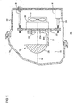
- FIG. 1 is a schematic cross-sectional view of an automotive lamp according to an embodiment of the present invention.
- An automotive lamp 10 is provided with a lamp body 12, a transparent cover 14, a lamp unit 18 housed in a lamp chamber 16 formed by the lamp body 12 and the transparent cover 14, and a bracket 20 serving as a support member that supports the lamp unit 18 in the lamp chamber 16.
- the lamp unit 18 is a projector-type lamp unit of a direct irradiation method and is provided with a light-emitting module 22 provided with a plurality of semiconductor light-emitting elements, a projection lens 24, and a connecting member 26 for connecting the projection lens 24 to the bracket 20.
- the light-emitting module 22 is provided with an LED 22a, which serves as a semiconductor light-emitting element, and a thermally-conductive insulating substrate 22b, which is formed by ceramics or the like.
- the light-emitting module 22 is placed on the bracket 20 such that the illumination axis of the light-emitting module 22 is directed in a forward direction of a vehicle, which is approximately parallel to an irradiation direction (a leftward direction in Fig. 10 ) of the lamp unit 18.
- the connecting member 26 has a planar part 26a and a curved part 26b.
- the planar part 26a is disposed approximately horizontally, and the curved part 26b is in an area in front of the planar part 26a.
- the shape of the curved part 26b is formed such that light emitted from the light-emitting module 22 is not reflected.
- the projection lens 24 is a plano-convex aspheric lens, having a convex front surface and a plane rear surface, which projects light emitted from the light-emitting module 22 toward a front area of the lamp.
- the projection lens 24 is disposed on a light axis Ax extending in frontward and rearward directions of the vehicle and is fixed to a tip end part of the connecting member 26 on the front side of the vehicle. Near a rear focal point of the projection lens 24, the LED chip 22a of the light-emitting module 22 is placed. Light emitted from the light-emitting module 22 directly enters the projection lens 24.
- the light that has entered the projection lens 24 is collected by the projection lens 24 and radiated in the forward direction as approximately parallel light beams.
- Fig. 2 is a perspective view illustrating an essential portion of the lamp unit 18 shown in Fig. 1 .
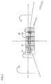
- Fig. 3 is a front view of the light-emitting module 22 shown in Fig. 1 .
- the light-emitting module 22 has a plurality of LED chips 22a.
- the total of twelve LED chips 22a are arranged in matrix on the thermally-conductive insulating substrate 22b, six chips 22a being arranged in a horizontal direction H and two chips 22a being arranged in a vertical direction V.
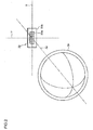
- screw holes 28 are formed at predetermined edge portions (three corner portions) of a square bracket 20.
- either one end of an aiming screw 30, either one end of an aiming screw 32, and either one end of a leveling shaft 34 are fixed, respectively.
- the respective other ends of the aiming screws 30 and 32 and the leveling shaft 34 are fixed in screw holes (not shown) of the lamp body 12.
- the bracket 20 is attached to the lamp body 12 in a condition where the bracket 20 is spaced forwardly apart from the rear surface of the lamp body 12.
- the automotive lamp 10 is configured such that the light axis of the lamp unit 18 can be adjusted in the horizontal direction or the vertical direction by the aiming screws 30 and 32, the leveling shaft 34, and a leveling actuator 36.
- a heat radiating fin 38 is provided on the rear side surface of the bracket 20. Further, between the heat radiating fin 38 and the lamp body 12, a fan 40 is provided that sends air toward the heat radiating fin 38 so as to cool the heat radiating fin 38.
- Fig. 4 is a view illustrating an example of a light distribution pattern formed by the automotive lamp 10 according to the embodiment of the present invention.
- the automotive lamp 10 shown in Fig. 1 is capable of forming a light distribution pattern PH in which a part of a region in front of a vehicle is not irradiated, as shown in Fig. 4 , by turning off some LED chips 22a of the light-emitting module 22.
- Twelve rectangular regions shown in Fig. 4 correspond to regions irradiated by respective LED chips, and regions shown with diagonal lines indicate a condition where light is being radiated.
- the automotive lamp 10 is capable of preventing glare casted onto a pedestrian 42, a leading vehicle 44, and an oncoming vehicle 46 by turning off respective LED chips that correspond to regions in which the pedestrian 42, the leading vehicle 44, and the oncoming vehicle 46 exist.
- Fig. 5 is a schematic sectional view illustrating an example of the light-emitting module according to the embodiment of the present invention.
- the light-emitting module 50 according to the embodiment of the present invention is provided with a first light-emitting unit 51a through a fourth light-emitting unit 51d.
- the first light-emitting unit 51a is provided with a semiconductor light-emitting element 52a.
- the second light-emitting unit 51b is provided with a semiconductor light-emitting element 52b.
- the third light-emitting unit 51c is provided with a semiconductor light-emitting element 52c.
- the fourth light-emitting unit 51d is provided with a semiconductor light-emitting element 52d.
- the semiconductor light-emitting elements 52a through 52d, which are arranged in a matrix, are mounted on a substrate 54.
- a fluorescent substance layer 58 is provided so as to face light-emitting surfaces 56a through 56d of the respective semiconductor light-emitting elements 52a through 52d.
- the fluorescent substance layer 58 functions as an optical wavelength conversion member that converts the wavelength of light emitted by the semiconductor light-emitting elements 52a through 52d, which are facing the fluorescent substance layer 58, so as to emit the light.
- the light-emitting module 50 may not be provided with a fluorescent substance layer 58.
- An interval W1 between light-emitting units is preferably smaller than a width W2 of a light-emitting unit.
- the interval W1 needs to be designed appropriately using experiments or previous findings while taking into consideration not to create a space between regions irradiated by the respective light-emitting units.
- the interval W1 between light-emitting units is preferably set, for example, in a range of 10 to 500 ⁇ m.
- Each light-emitting unit can emit light of various colors by a combination of a semiconductor light-emitting element and a fluorescent substrate.
- a light-emitting unit may be used that realizes white light by a combination of a semiconductor light-emitting element that emits blue light and a fluorescent substance that absorbs blue light and converts the light to yellow light.
- a light-emitting unit may be used that realizes white light by a combination of a semiconductor light-emitting element that emits ultraviolet light, a first fluorescent substance that absorbs ultraviolet light and converts the light to blue light, and a second fluorescent substance that absorbs ultraviolet light and converts the light to yellow light.
- light-shielding portions 60a through 60d are provided so as to cover the sides and the lower surfaces of the respective semiconductor light-emitting elements.
- the light-shielding portions 60a through 60d may be separated from one another or may be formed in an integral manner as shown in Fig. 5 .
- the light-shielding portions 60a through 60d may be provided to surround the perimeter of respective light-emitting surfaces of at least some semiconductor light-emitting elements among the plurality of semiconductor light-emitting elements.
- the part of the light is shielded by the light-shielding portion 60a.
- the part of the light is shielded by the light-shielding portion 60b. Also, even when a part of light of the semiconductor light-emitting element 52c is radiated toward the fluorescent substance layer 58 of regions 62a and 62d facing the light-emitting surfaces 56a and 56c of the adjacent semiconductor light-emitting elements 52a and 52c, respectively, the part of the light is shielded by the light-shielding portion 60b. Also, even when a part of light of the semiconductor light-emitting element 52c is radiated toward the fluorescent substance layer 58 of regions 62b and 62d facing the light-emitting surfaces 56b and 56d of the adjacent semiconductor light-emitting elements 52b and 52d, respectively, the part of the light is shielded by the light-shielding portion 60c.
- the part of the light is shielded by the light-shielding portion 60d.
- the fluorescent substance layer 58 of a region facing a light-emitting surface of an adjacent semiconductor light-emitting element is prevented from lighting up due to light emitted from at least one semiconductor light-emitting element.
- the light-emitting unit 51a is turned on and the light-emitting unit 51b adjacent to the light-emitting unit 51a is turned off, a region subjected to irradiation of the light-emitting unit 51b is prevented from being illuminated unintentionally.
- the part of the light is shielded by a light-shielding portion that covers the side surface of the semiconductor light-emitting element.
- the automotive lamp 10 is prevented from casting glare onto a passenger of a vehicle or a pedestrian in a region corresponding to a semiconductor light-emitting element that is turned off, when a light distribution pattern such as the one shown in Fig. 4 is formed.
- the above described condition of being "arranged in a matrix” includes at least a case where a plurality of light-emitting elements are arranged in m ⁇ 1 (m is an integer of 2 or more), 1 ⁇ n (n is an integer of 2 or more), m ⁇ n (m and n are both integers of 2 or more). Two arrangement directions do not need to be always perpendicular to each other, and the light-emitting elements may be arranged in a range of a parallelogram or a trapezoid as a whole.
- the plurality of the light-emitting elements may not all be of a single type and may be of a combination of a plurality of types of light-emitting elements.
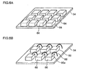
- Fig. 6A is a schematic diagram for explaining the structure of an LED chip that is suitable for the light-emitting module according to the embodiment of the present invention
- Fig. 6B is a schematic diagram illustrating the structure of an LED chip according to a comparative example.
- an LED chip 64 of a face-down type (flip-chip type) (see Fig. 6A ) or an LED chip 66 of a face-up type (see Fig. 6B ) are considered to be employed.
- Fig. 7 is a schematic diagram illustrating a condition where LED chips of different sizes are arranged in a matrix.
- a light-emitting module When a light-emitting module is applied in an automotive lamp, there is a region called a hot zone in a light distribution pattern of a headlamp that requires high luminance (e.g., 80000 cd or more). Accordingly, large-size (e.g., 1 mm ⁇ 1 mm) LED chips 70 that form a hot zone are arranged in the center part on the substrate. Meanwhile, small-size (e.g., 0.3 mm ⁇ 0.3 mm) LED chips 72 are arranged in the surrounding part thereof for a reduction of cost. With this, a light-emitting module can be realized with a cost reduction while allowing for the formation of a hot zone.
- large-size (e.g., 1 mm ⁇ 1 mm) LED chips 70 that form a hot zone are arranged in the center part on the substrate.
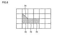
- Fig. 8 is a schematic diagram illustrating a condition where LED chips of different shapes are arranged in a matrix.
- a light-emitting module When a light-emitting module is applied in an automotive lamp, there is a case where the formation of a light distribution pattern for low beam having a diagonal cut-off line at a part of the upper portion of a light distribution pattern is required. Accordingly, a triangle LED chip 74 that forms a diagonal cut-off line at a part on the substrate is arranged. Meanwhile, regular LED chips 70 are arranged in the surrounding part thereof.
- the hypotenuse of the LED chip 74 preferable has a degree of about 10 to 60 with respect to the horizontal direction. More preferably, the hypotenuse of the LED chip 74 has a degree of 15, 30, 45, or the like.
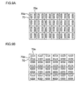
- Fig. 9A is a schematic diagram illustrating a state where electrode portions of LED chips are arranged in a longitudinal direction
- Fig. 9B is a schematic diagram illustrating a state where electrode portions of LED chips are arranged in a traverse direction.
- luminance is relatively low in electrode portions 70a, and luminance is relatively high in the center part between the electrodes 70a.
- luminance is uneven in a light-emitting surface.
- there are spaces between LED chips about 100 to 300 ⁇ m
- the luminance at the parts are obviously decreased, causing unevenness in luminance in the entire light-emitting module.
- Such unevenness in luminance often appears as a shadow (black line) in a light distribution pattern.
- the LED chips 70 are arranged such that the electrode direction is in the longitudinal direction, as shown in Fig. 9A .
- the LED chips 70 are arranged such that the electrode direction is in the traverse direction, as shown in Fig. 9B .
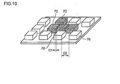
- Fig. 10 is a schematic diagram illustrating a condition where intervals between LED chips are changed by location.
- intervals C1 between the chips are narrowed, and the density in the arrangement of the chips is high.
- the luminance of the hot zone in a light-distribution pattern can be increased.
- intervals C2 between the chips are widened, and the density in the arrangement of the chips is low.
- the number of chips that irradiate the surrounding part of a light distribution pattern can be reduced, allowing for a reduction in cost for the entire light-emitting module.
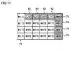
- Fig. 11 is a schematic diagram illustrating a condition where a plurality of types of LED chips of different emission wavelengths are arranged.
- a light-emitting module shown in Fig. 11 is provided with LED chips 70 that emit white light and LED chips 78 that emit amber light.
- LED chips 70 that emit white light
- LED chips 78 that emit amber light.
- an automotive lamp can be realized in which a headlight and a turn signal lamp are integrated.
- LED chips 80 that emit ultraviolet light (UV) and LED chips 82 that emit infrared light (IR) a light-source function for a night-vision camera can be added to the light-emitting module.
- UV ultraviolet light
- IR infrared light
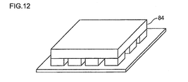
- Fig. 12 is a schematic diagram illustrating a condition where a plurality of LED chips formed on a single epitaxial substrate are mounted on a mounting substrate.
- a plurality of LED chips are formed on a single epitaxial substrate 84, and portions of the epitaxial substrate between the chips are electrically cut (integral in a physical manner) by half-cut using a dicing blade so as to separate the epitaxial substrate for each individual LED chip. With this, spaces between the chips can be reduced, and light modulation can be individually performed on each LED chip.
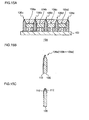
- Fig. 13A is a schematic diagram illustrating a condition where, of LED chips arranged in a matrix, LED chips of some lines (rows) are displaced
- Fig. 13B is a schematic diagram illustrating a condition where a plurality of rectangular LED chips are arranged at an angle and in a matrix.
- LED chips 86 arranged in the center row are displaced in the right direction in the figure by a distance C3 with respect to LED chips 88 arranged in the front row or the back row.
- spaces between the LED chips 86 arranged in the center row are displaced by the distance C3 with respect to respective spaces between the LED chips 88 arranged in the front row or the back row.
- a black line in the longitudinal direction (vertical direction) in a light distribution pattern that is formed by the light-emitting module becomes unnoticeable.
- LED chips 90 are arranged in a matrix and in a diagonal manner so that spaces between adjacent LED chips 90 are diagonal. Therefore, black lines in the longitudinal direction (vertical direction) and in the traverse direction (horizontal direction) in a light distribution pattern formed by the light-emitting module become unnoticeable.
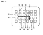
- Fig. 14 is a schematic diagram illustrating a condition where a light-shielding frame is provided only around some LED chips.
- a light-shielding frame such that the light-shielding frame surrounds the perimeter of a light-emitting surface.
- spaces between LED chips are widened too much, a dark shadow will be projected on a part of a light distribution pattern.
- the spaces between the LED chips cannot be widened too much, and the thickness of the light-shielding frame have to be reduced.
- a light-shielding frame is provided for all the LED chips, the size of components will become increased.
- Microfabrication is required for the preparation of a thin light-shielding frame.
- the size of a light-shielding frame is increased, the preparation becomes more difficult, and the production cost may be increased due to a decrease in the yield and an increase in the production time.
- LED chips 70 arranged in the center part on the substrate and forming a hot zone.
- the luminance when turned on is relatively high in such LED chips 70.
- LED chips 92 whose luminance when turned on is relatively low are arranged around the LED chips 70.
- a light-shielding frame 94 is mainly provided between an LED chip 70 and an LED chip 92 adjacent to the LED chip 70.
- Fig. 15A is a schematic sectional view of a light-emitting module in which a light-shielding film is formed on a part of the side of a light-shielding frame
- Fig. 15B is an enlarged view of a part of the light-shielding frame shown in Fig. 15A
- Fig. 15C is a view illustrating an exemplary variation of the part of the light-shielding frame shown in Fig. 15B .
- a light-emitting module 100 is provided with a substrate 102, flip-chip type LED chips 104a through 104d arranged on the substrate 102, and light-shielding frames 106a through 106e arranged around respective LED units.
- the light-shielding frames 106a through 106e each have a body portion 108 made of a transparent material such as a glass and formed in a thin plate shape and a colored portion 110 formed on one side of the body portion 108.
- the material and the thickness of the colored portion 110 are not particularly limited as long as the colored portion 110 functions as a light-shielding film that shield light. With this, the width of a portion of a light-shielding frame 106 that functions as a light-shielding portion can be reduced, and the formation of a shadow in a light distribution pattern can be prevented.
- a light-shielding frame in which colored portions 112 are formed at the top of a body portion 108 may be used.
- the configuration of a colored portion is not particularly limited as long as the colored portion substantially functions as a light-shielding portion.
- the colored portion needs to reflect or attenuate at least a part of light.
- Fig. 16 is a schematic diagram illustrating a condition where the thickness of a part of a light-shielding frame is reduced.
- a reduction in the thickness of a light-shielding frame 114 comes with production difficulty. Accordingly, the thickness of a light-shielding frame is reduced only for a part whose thickness is particularly required to be reduced, and, for the other part, the thickness of the light-shielding frame is set to be a thickness that allows for easy production.
- LED chips 70 forming a hot zone are arranged in the center part on the substrate.
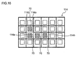
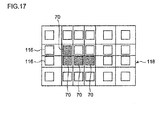
- Fig. 17 is a schematic diagram illustrating a condition where the area of a region in which a light-shielding frame surrounds LED chips is changed according to a chip.
- the area of a region surrounding one of LED chips 70 that form a hot zone is smaller than the area of a region surrounding one of LED chips 116 that surrounds the LED chips 70.
- a light-shielding frame 118 surrounding the LED chips 70 is configured such that the size of a plurality of partitioned regions varies by location.
- the LED chips 70 that form the hot zone can be arranged in a more concentrated manner, and the maximum luminance of the hot zone can be increased.
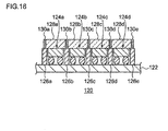
- Fig. 18 is a schematic sectional view of a light-emitting module in which a light-shielding film is formed on the side of a fluorescent substance.
- a light-emitting module 120 is provided with a substrate 122, flip-chip type LED chips 124a through 124d arranged on the substrate 122, light-shielding frames 126a through 126e arranged around respective LED units, and fluorescent substance layers 128a through 128d provided above the respective LED units.
- Light-shielding films 130a through 130e are formed on the respective side surfaces of the fluorescent substance layers 128a through 128d.
- the light-shielding films 130a through 130e are formed by, for example, a metal or an alloy.
- light-shielding portions are formed by the light-shielding frames 126a through 126e and the light-shielding films 130a through 130e. With this, the shape of a light-shielding frame can be simplified.
- Fig. 19 is a schematic diagram illustrating a condition where a reflective film is formed on a part of a light-shielding frame.
- a light-emitting module 132 light-shielding frames 134a through 134e are provided between the LED chips 124a through 124d and between the fluorescent substance layers 128a through 128d.
- the light-shielding frames 134a through 134e (hereinafter referred to as light-shielding frames 134) have vertical portions 136a adjacent to the respective sides of the LED chips 124a through 124d and taper portions 136b that are located above the respective vertical portions 136a and that are adjacent to the respective sides of the fluorescent substance layers 128a through 128d.
- luminance that can be achieved by a light-emitting module can be increased by forming reflective films on all the light-shielding frames 134.
- reflective films are formed on the taper portions 136b, fluorescence from the fluorescent substance layers 128a through 128d are mainly reflected, causing unevenness in color.
- reflective films are not formed on the taper portions 136b (fluorescent substance layer portions), and reflective films 138 are formed only on the respective sides of the vertical portions 136a. With this, a light-emitting module with less unevenness in color can be realized.
- Fig. 20 is a schematic sectional view of a light-emitting module in which an ultraviolet light-emitting chip is used as an LED chip.
- a white LED is usually formed with a blue light-emitting LED chip and a yellow fluorescent substance. In this configuration, blue transmitted light is likely to be split, and unevenness in color is likely to be caused.
- a light-emitting module 140 is provided with LED chips 142a through 142d that emit ultraviolet light and fluorescent substance layers 144a through 144d provided such that the fluorescent substance layers 144a through 144d face respective light-emitting surfaces of the LED chips 142a through 142d.
- the fluorescent substance layers 144a through 144d include blue fluorescent substances that are excited by ultraviolet light to emit blue light and yellow fluorescent substances that are excited by ultraviolet light to emit yellow light.
- Light-shielding frames 146a through 146e are provided between the LED chips 142a through 142d and between the fluorescent substance layers 144a through 144d.
- the light-emitting module 140 chips of an ultraviolet light-emitting type are used as LED chips, and unevenness in color is thus not likely to be caused. Therefore, reflective films 148 can be formed on the entire side surfaces of the light-shielding frames 146a through 146e, and the configuration is more simple compared to a case when reflective films are formed only on a part of the side surfaces of the light-shielding frames. Thus, the production of the light-shielding frames is facilitated.
- Fig. 21 is a schematic diagram illustrating a light-emitting module in which the shape of a region partitioned by a frame is hexagonal.
- a light-shielding frame 152 provided in a light-emitting module 150, the shape of a region that surrounds one of LED chips 70 is hexagonal. If the shape of a partition of the light-shielding frame is square, a shadow is projected onto a light distribution pattern in the longitudinal direction (vertical direction) and the traverse direction (horizontal direction).
- the shape of a partition of the light-shielding frame is hexagonal, a shadow is projected onto a light distribution pattern in the directions other than in the longitudinal direction (vertical direction), the traverse direction (horizontal direction). Therefore, a shadow created in a light distribution pattern becomes less noticeable.
- the shape of the region partitioned by the frame may be polygonal such as octagonal or pentagonal.
- the composition of a fluorescent substance layer is not particularly limited as long as the fluorescent substance layer can be applied to the a variety of light-emitting modules that have been described previously.
- the composition includes a resin composition or a glass composition with dispersed fluorescent substances and a fluorescent ceramic.
- some preferred modes are exemplified as the composition of a fluorescent substance.
- Mixing of blue light and yellow light or mixing of red light, blue light, and green light is important in order to reduce unevenness in brightness and color among white LED chips.
- uniformly diffuse (disperse) fluorescent substances (phosphors) in a fluorescent substance layer examples include the following composition.
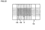
- Fig. 22 is a schematic diagram illustrating a condition where the size of a fluorescent substance layer that is partitioned varies by location.
- the size of a single section 156 in a region R (dotted region) facing LED chips that form a hot zone is set to be smaller than the size of a section 158 in the other region. With this, the luminance of the hot zone in a light distribution pattern formed by a light-emitting module can be increased.
- Figs. 23A to 23G are schematic sectional views for explaining the shape of a fluorescent substance layer.
- a fluorescent substance layer is formed within a light-shielding frame for shielding light.
- the fluorescent substance layer is preferably a plate-like fluorescent substance. With this, the processing of a fluorescent substance is facilitated.
- various sorts of surface processing e.g., formation of concavities and convexities for improving the brightness becomes possible.
- a fluorescent substance layer 160 shown in Fig. 23A has a trapezoidal shape.
- a fluorescent substance layer 162 shown in Fig. 23B has a Y shape.
- On the side surfaces of a fluorescent substance layer 166 shown in Fig. 23C reflective portions 168 are formed.
- On the side surfaces of a fluorescent substance layer 170 shown in Fig. 23d light-shielding portions 172 are formed.
- a fluorescent substance layer 174 shown in Fig. 23E has a trapezoidal shape, and a wavelength-selective filter 176 is formed on the side surface and the bottom surface of the fluorescent substance layer 174. Therefore, in light emitted from an LED chip 178, light of a wavelength selected by the wavelength-selective filter 176 reaches the fluorescent substance layer 174.
- a light diffusion phase 182 is provided above an emission surface 180a. This allows for a reduction in unevenness in the brightness of light emitted from the fluorescent substance layer 180.
- a light diffusion phase 186 is provided below an incident surface 184a. With this, unevenness in the brightness of light emitted from an LED chip 188 is reduced by the light diffusion phase 186, and the light then enters the fluorescent substance layer 184.
- the light diffusion phase and the fluorescent substance layer are preferably connected without using an adhesive by a method such as thermal compression bonding, normal temperature bonding, or the like. Thereby, scattering and attenuation of light when the light passes through an adhesive layer can be prevented, and an efficiency of extracting light from the entire light-emitting module is thus improved.
- Figs. 24A to 24F are schematic sectional views for explaining the arrangement of a fluorescent substance layer in a light-emitting module. Since a fluorescent substance layer is separated from an LED chip or combined with a lens, a light-guiding plate, a reflecting mirror, or the like in consideration of the improvement in the brightness and the prevention of unevenness in color, the fluorescent substance can have various arrangements.
- a fluorescent substance layer 190 shown in Fig. 24A is arranged at a position spaced apart from an LED chip 192. With this, the heat dissipation of the LED chip 192 or the fluorescent substance layer 190 is improved, and the properties of the entire light-emitting module are improved.
- the fluorescent substance layer 190 is surrounded by a light-shielding frame 194 and has an emission surface 190a, whose area is smaller that that of a light-emitting surface 192a of the LED chip 192. With this, the brightness of the light-emitting module is improved.
- a lens 198 is provided in front of an emission surface 196a. With this, light emitted from the fluorescent substance layer 196 can be collected.
- a fluorescent substance layer 200 shown in Fig. 24C is provided such that the center 200a thereof is not aligned with the center 202a of an LED chip 202.
- a fluorescent substance layer 204 shown in Fig. 24D is arranged above an emission surface 206a of a light-guiding plate 206.
- An incident surface 206b of the light-guiding plate faces a light-emitting surface 208a of an LED chip 208.
- light emitted by the LED chip 208 enters the fluorescent substance layer 204 after passing through the light-guiding plate 206, and a range irradiated by the light is thereby controlled. With this, light leakage among a plurality of LED chips can be prevented.
- the light-guiding plate 206 has a translucent (transparent) material that allows for the penetration of light emitted by an LED chip.
- the translucent material include, for example, an organic material such as a transparent resin material or the like, an inorganic material such as a transparent inorganic glass or the like, a mixture of an organic material and an inorganic material, a sol-gel material, and the like.
- the resin material include an acrylic resin, a polycarbonate resin, an epoxy resin, and the like.
- a light-emitting module shown in Fig. 24E is characterized in that a lens 210 is arranged between a fluorescent substance layer 190 and an LED chip 192. With this, light emitted by the LED chip 192 is collected by the lens 210 and then enters the fluorescent substance layer 190.
- a light-emitting module shown in Fig. 24F is characterized in that light heading beneath the LED chip 192 is collected using a reflecting mirror 212 and then directed toward the fluorescent substance layer 190.
- Fig. 25A is a schematic diagram illustrating a condition where a fluorescent substance layer is created for each section by a potting method
- Figs. 25B to 25D are schematic diagrams illustrating a condition where fluorescent substance layers are created all at once by a printing method.
- Fig. 25B shows a case when printing is performed in a printing direction that is along the direction of a diagonal line of each section corresponding to an LED chip.
- Fig. 25C shows a case when printing is performed in a printing direction that is along the longitudinal sides of each section corresponding to an LED chip.
- Fig. 25D shows a case when printing is performed in a printing direction that is along the traverse sides of each section corresponding to an LED chip.
- a fluorescent substance layer 214 a plurality of fluorescent substances 214a, which are partitioned to correspond to respective LED chips, are arranged in a matrix.
- a rectangular unevenness 214b is formed inside each side of a section and is visually noticeable.
- a method for forming a fluorescent substance layer includes a forming method of mixing a powder fluorescent substance with a resin to make a paste and then shaping the paste into a layer by printing. As shown in Figs. 25B through 25D , by aligning a printing direction in a single direction, color unevennesses 214c through 214e can be controlled in a given direction.
- a light-emitting module is equipped with many LED chips on a single mounting substrate.
- the linear expansion coefficient of the mounting substrate is defined to be within a range of ⁇ 5 ppm/°C of the thermal expansion coefficient of the LED chips. With this, a decrease in connection reliability created by temperature changes repeated by turning on or off the LED chips can be prevented. If the LED chips are GaN, the thermal expansion coefficient thereof is about 7 ppm/°C.
- the main components of the mounting substrate are preferably alumina, AlN, Si, SiO 2 , and the like.
- a light-emitting module is equipped with many LED chips on a single mounting substrate.
- the thermal conductivity of the mounting substrate is preferably increased in a range that does not greatly affect other performance of the light-emitting module.
- a mounting substrate may be employed where a part of the mounting substrate on which LED chips that irradiate a region corresponding to a hot zone has higher thermal conductivity compared to the other part.
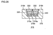
- Fig. 26 is a schematic sectional view illustrating an example of a mounting substrate.
- a light-emitting module 216 is provided with a mounting substrate 218, LED chips 220 arranged on respective concave portions 218a of the mounting substrate 218, and a fluorescent substance layer 222 arranged above the LED chips.
- the concave portions 218a are formed by engraving the mounting substrate 218. Therefore, a light-shielding portion 218b is formed at the same time such that the light-shielding portion 218b surrounds the concave portions 218a.
- the concave portions 218a by engraving the mounting substrate 218, the arrangement of a light-shielding frame on the substrate as a different component is no longer necessary. As a result, the man-hour for the assembly of the light-emitting module is reduced, allowing for a reduction in cost.
- silicon can be used as a material of the mounting substrate.
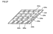
- Fig. 27 is a schematic diagram illustrating a mounting substrate having a double-sided wiring.
- a mounting substrate 224 having double-sided wiring is preferably used when there are three or more rows of LED chips.
- a wiring 228a connected to an LED chip 226a located on a front row and a wiring 228c connected to an LED chip 226c located on a back row are formed on a front surface 224a of the mounting substrate 224.
- a wiring 228b connected to an LED chip 226b located on a middle row is formed on a back surface 224b of the mounting substrate 224. With this, the area of the substrate can be reduced.
- Stray light is preferably prevented by allowing the above-stated reflective portions to have color that absorbs light (such as black), except for a light reflective surface above the light-emitting surface of an LED chip.
- a lens is connected to a fluorescent substrate layer.
- the lens may be connected to an LED chip.
- Such a lens may project a light-source image, which is created by light emitted from the LED chip and the fluorescent substance layer, on a virtual vertical screen provided in front in an irradiation direction.
- the connection is preferably achieved without using an organic adhesive material. This is because the probability of scattering and bending at an interface between layers is increased if the number of unnecessary layer is increased.
- the lens and the fluorescent substance layer or the like are connected without any adhesives by a various methods such as normal temperature bonding, interfacial activation bonding, anodic bonding, and the like. With this, light from the LED chip or light passed through the fluorescent substance layer becomes less likely to be absorbed or reflected at an interface with the lens, and luminous flux emitted from the light-emitting module is improved.
- a substrate or a light-shielding frame is made of silicon and a glass used for a lens contains an alkali metal
- the substrate or the light-shielding frame can be anodically bonded (anodic bonding is a technique for achieving bonding by applying heat of about 500°C and a voltage of about 500 V to diffuse an alkali metal in a glass in silicon) with the lens. With this, hermetic sealing of the light-emitting module is possible.
- the linear expansion coefficient of the glass is preferably set to be close to 3 ppm/°C, which is the linear expansion coefficient of silicon. More specifically, the glass used for the lens is preferably a material whose linear expansion coefficient is in a range of 1 to 10 ppm/°C.
- a lens array may be mounted on the above-stated light-emitting module in which LED chips are arranged in an array (in a matrix).
- a lens array is designed such that a plurality of lenses corresponding to respective LED chips are formed on a single plate-like member.
- Such a lens array is disclosed in, for example, PCT Japanese Translation Patent Publication No. 2006-520518 . Since a light-emitting module according to the embodiment of the present invention is provided with a light-shielding portion, light leakage can be prevented even when such a lens array is used. Also, a reduction of cost may be achieved by making the lens array by integral molding by a resin.
- a CPC lens may be used as a type of the lens array. With this, an color unevenness in an individual light-emitting unit can be overcome.
- a lens may be shaded only in the longitudinal direction. If a dark part created between light-emitting units (a single LED chip and a single fluorescent substance) is projected in the longitudinal direction as a black line when an LED array is all turned on, the projection lens 24 (PES lens) shown in Fig. 1 or the like, which is the last lens that emits light, may be shaded in the longitudinal direction.
- the projection lens 24 PES lens shown in Fig. 1 or the like, which is the last lens that emits light
- the lens may be shaded only in the traverse direction. If a dark part created between light-emitting units is projected in the traverse direction as a black line when the LED array is all turned on, the projection lens 24 shown in Fig. 1 may be shaded in the traverse direction.
- the lens may be shaded only in the oblique direction. If a dark part created between light-emitting units is projected in the oblique direction as a black line when the LED array is all turned on, the projection lens 24 shown in Fig. 1 may be shaded in the oblique direction. Shading in the longitudinal direction, in the traverse direction, and in the oblique direction may be appropriately combined.
- a brightness unevenness and a color unevenness may be reduced by using an optical fiber array.
- a light-guiding plate layer in which optical fibers are put into a bundle on an LED chip or on a fluorescent substance layer By providing a light-guiding plate layer in which optical fibers are put into a bundle on an LED chip or on a fluorescent substance layer, a brightness unevenness and a color unevenness can be reduced.
- a flat-plate microlens may be provided.
- An optical lens may be formed by distributing components having a high or low refractive index in a plate-like transparent body (GRIN lens).
- a configuration is preferred in which such an air layer does not lie therebetween.
- a space between the projection lens 24 and the light-emitting module 22 is preferably filled with a silicone gel.
- the light-emitting module can be applied to an automotive lamp (headlamp) of a different design.
- a fluorescent substance may be processed into a lens shape and may be mounted on an LED chip so as to form a light-emitting module. Since the fluorescent substance has a convex lens shape, there is no trapping of light due to a critical angle. Thus, luminous flux is improved for the light-emitting module as a whole.
- the automotive lamp 10 shown in Fig. 1 is provided with a light-emitting module 22 and a control circuit (not shown) that controls the turning on and off of the light-emitting module 22. If the control circuit detects a condition where a vehicle provided with the automotive lamp is stopped, the control circuit controls the turned-on or turned-off condition of the light-emitting module so as to enter a vehicle stop mode where the power consumption is smaller than that during an irradiation mode used when the vehicle is running. This allows for the power saving of an automotive lamp without requiring an operation by a driver.
- the above-stated control circuit is capable of performing turning-on and turning-off control of an LED of a light-emitting module. Since the speed of the turning on and off of the LED is fast, information can be transmitted by pulse lighting.
- the control circuit be provided with a function of controlling communication between vehicles (the driver's own car and another car) and between a road and a vehicle (traffic light and vehicle or the like) in addition to a function for turning-on and turning-off control for ADB (Adaptive Driving Beam).
- the control circuit of the automotive lamp 10 increases the light intensity of the light-emitting module 22 if the control circuit detects the moment of collision based on information from a detection means that detects the moment of the collision. With this, accidents can be clearly recorded by the image-capturing means provided in the vehicle.
- a main purpose of the light-distribution control by ADB is to partially turn off some of a plurality of LED chips in order for the prevention of glare.
- the control circuit may perform control of increasing, in a spotted manner, the light intensity of an LED chip that irradiates a region in which the pedestrian exists in order to alert the driver.
- a light-emitting module by using exemplary embodiments and comparative examples in the following.
- four blue LED chips of a size of 1 ⁇ 1 mm and of a light-emission peak wavelength of 450 nm are mounted on a mounting substrate made of aluminum nitride that is wired such that light modulation could be performed for each individual LED.
- a light-shielding frame obtained by performing microfabrication on silicon is mounted, and a fluorescent substance layer is implemented so as to prepare an LED package (hereinafter, referred to as "light-emitting module").
- This light-emitting module is placed on a heat sink made of die-cast aluminum and is stabilized for ten minutes while applying an electric current of 700 mA to the four LED chips.
- the brightness is measured by a two-dimensional color luminance meter CA1500 manufactured by Konica Minolta from the front surface (the upper surface of the light-emitting module) of a light-emitting surface of the light-emitting module so as to measure a brightness distribution in the longitudinal direction of the light-emitting module.
- the longitudinal direction is a direction in which the approximate centers of respective light-emitting surfaces of the LED chips are connected.
- the electric current of one LED chip is then blocked, and a brightness distribution is measured. Further, the brightness of a turned-off portion is measured.
- the light-emitting module in which the brightness of the turned-off portion is low enough to allow for the shielding of light, is placed in a lamp provided with a plano-convex lens of ⁇ 60 with a focal length of 40 mm.
- the light-emitting module is turned on and projected to a screen that is located 25 m ahead, and a luminance distribution is measured. Then, in the same way as in the brightness measurement, the electric current of one LED is blocked, and a luminance distribution is measured again.
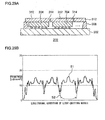
- Fig. 28A is a schematic sectional view of a light-emitting module according to comparative example 1
- Fig. 28B is a view illustrating a graph of a brightness distribution of the light-emitting module according to comparative example 1.
- a curve S1 represents a brightness distribution when all the four LEDs are turned on
- a curve S2 represents a brightness distribution when only one LED is turned off. The same applies to a brightness distribution in the following exemplary embodiments.
- a light-emitting module 300 according to a comparative example 1 is provided with a substrate 302, a plurality of LED chips 304 mounted on the substrate 302, a fluorescent substance layer 306 composed of a single YAG sintered compact of a size that covers the plurality of LED chips 304, and an outer frame 308, which is held by the substrate 302 and which supports the periphery of the fluorescent substance layer 306.
- neither an individual LED chip 304 nor the fluorescent substance layer 306 has a structure (configuration) for optically separating (shielding light) adjacent light-emitting portions (light-emitting surfaces). Therefore, even when one LED chip is turned off, the brightness of the portion is 1.5 cd/mm 2 (the lowest part of a curve S2 shown in Fig. 28B ), and light shielding is thus not sufficient.
- Fig. 29A is a schematic sectional view of a light-emitting module according to exemplary embodiment 1
- Fig. 29B is a view illustrating a graph of a brightness distribution of the light-emitting module according to exemplary embodiment 1.
- like numerals represent like constituting elements in the comparative example 1, and the description thereof is appropriately omitted.
- each fluorescent substance layer 312 is composed of a YAG sintered compact of a size that covers a single LED chip 304, and a silver paste 314 is applied to the side surfaces thereof. With this, light emitted from an adjacent fluorescent substance layer 312 is shielded. As a result, when one LED chip is turned off, the brightness of the portion is greatly reduced to be 0.3 cd/mm 2 (the lowest part of a curve S2 shown in Fig. 29B ), showing a light-shielding effect.
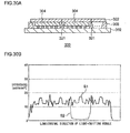
- Fig. 30A is a schematic sectional view of a light-emitting module according to exemplary embodiment 2
- Fig. 30B is a view illustrating a graph of a brightness distribution of the light-emitting module according to exemplary embodiment 2.
- like numerals represent like constituting elements described previously, and the description thereof is appropriately omitted.
- a triangle frame 321 obtained by performing microfabrication on silicon is placed between LED chips 304 so as to shield light. With this, light emitted from an adjacent LED chip 304 is shielded. Meanwhile, a fluorescent substance layer 322 is composed of a YAG sintered compact of a size covering a single LED chip 304, and nothing is applied to the side surfaces thereof. As a result, when one LED chip is turned off, the brightness of the portion is greatly reduced to be 0.6 cd/mm 2 (the lowest part of a curve S2 shown in Fig. 30B ), showing a light-shielding effect.
- the light-emitting module 320 is integrated in a lamp, and a luminance distribution is measured.
- the minimum luminance when one LED chip is turned off is 500 cd, and it is found that the luminance is below a luminance of 625 cd at which glare might be casted onto oncoming vehicles, leading vehicles, and pedestrians.
- the exemplary embodiment 2 it is found that, as long as the brightness of a turned-off portion of the light-emitting module is 0.6 cd/mm 2 or below, the production of glare when applied to a lamp can be prevented.
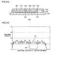
- Fig. 31A is a schematic sectional view of a light-emitting module according to exemplary embodiment 3
- Fig. 31B is a view illustrating a graph of a brightness distribution of the light-emitting module according to exemplary embodiment 3.
- like numerals represent like constituting elements described previously, and the description thereof is appropriately omitted.
- a triangle frame 321 obtained by performing microfabrication on silicon is placed between LED chips 304 so as to shield light. With this, light emitted from an adjacent LED chip 304 is shielded.
- each fluorescent substance layer 312 is composed of a YAG sintered compact of a size that covers a single LED chip 304, and a silver paste 314 is applied to the side surfaces thereof. With this, light emitted from an adjacent fluorescent substance layer 312 is shielded.
- the brightness of the portion is greatly reduced to be 0.3 cd/mm 2 (the lowest part of a curve S2 shown in Fig. 31B ), showing a light-shielding effect.
- Fig. 32A is a schematic sectional view of a light-emitting module according to exemplary embodiment 4
- Fig. 32B is a view illustrating a graph of a brightness distribution of the light-emitting module according to exemplary embodiment 4.
- like numerals represent like constituting elements described previously, and the description thereof is appropriately omitted.
- a triangle frame 342 obtained by performing microfabrication on silicon is placed between LED chips 304 so as to shield light. With this, light emitted from an adjacent LED chip 304 is shielded.
- the apex of the triangle frame 342 is located near the front surface of a fluorescent substance layer 344.
- Each fluorescent substance layer 344 is composed of a YAG sintered compact of a size covering a single LED chip 304. With this, light emitted from an adjacent fluorescent substance layer 344 is shielded.
- the brightness of the portion is greatly reduced to be 0 cd/mm 2 (the lowest part of a curve S2 shown in Fig. 32B ), showing a light-shielding effect.
- the light-emitting module 340 is integrated in a lamp, and a luminance distribution is measured.
- the minimum luminance when one LED chip is turned off is 300 cd, and it is confirmed that the luminance is below a luminance of 625 cd at which glare might be casted onto oncoming vehicles, leading vehicles, and pedestrians.
- Fig. 33A is a schematic sectional view of a light-emitting module according to exemplary embodiment 5
- Fig. 33B is a view illustrating a graph of a brightness distribution of the light-emitting module according to exemplary embodiment 5.
- Fig. 33B shows only a brightness distribution (curve S1) when all the four LEDs are turned on.
- like numerals represent like constituting elements described previously, and the description thereof is appropriately omitted.
- a triangle frame 342 obtained by performing microfabrication on silicon is placed between LED chips 304 so as to shield light. With this, light emitted from an adjacent LED chip 304 is shielded.
- the apex of the triangle frame 342 is exposed through the front surface of a fluorescent substance layer 352.
- the fluorescent substance layer 352 is formed by printing a paste, in which YAG powder is mixed in a dimethyl silicone resin to account for 12 volume percent, on the LED chips 304 with use of a squeegee.
- the tip of the triangle frame 342 is adjusted at that time such that the tip is exposed. With this, light emitted from an adjacent fluorescent substance layer 352 is shielded.
- the brightness of the portion is greatly reduced to be 0 cd/mm 2 , showing a light-shielding effect.
- the light-emitting module 340 is integrated in a lamp, and a luminance distribution is measured.
- the minimum luminance when one LED chip is turned off is 300 cd or below, and it is confirmed that the luminance is below a luminance of 625 cd at which glare might be casted onto oncoming vehicles, leading vehicles, and pedestrians.
- Fig. 34A is a schematic sectional view of a light-emitting module according to exemplary embodiment 6, and Fig. 34B is a view illustrating a graph of a brightness distribution of the light-emitting module according to exemplary embodiment 6.
- Fig. 34B shows only a brightness distribution (curve S1) when all the four LEDs are turned on.
- like numerals represent like constituting elements described previously, and the description thereof is appropriately omitted.
- a vertical frame 362 obtained by performing microfabrication on silicon is placed between LED chips 304 so as to shield light.
- the vertical frame 362 is provided such that the side surfaces thereof are approximately vertical to the front surface of a substrate 302. With this, operations and effects that are similar to those according to the exemplary embodiment 5 are obtained.
- Fig. 35A is a schematic sectional view of a light-emitting module according to exemplary embodiment 7, and Fig. 35B is a view illustrating a graph of a brightness distribution of the light-emitting module according to exemplary embodiment 7.
- Fig. 35B shows only a brightness distribution (curve S1) when all the four LEDs are turned on.
- like numerals represent like constituting elements described previously, and the description thereof is appropriately omitted.
- a frame 372 obtained by performing microfabrication on silicon is placed between LED chips 304 so as to shield light.
- the frame 372 is provided such that a side surface thereof on the side close to a substrate 302 (a lower part in Fig. 35A ) is approximately vertical to the front surface of the substrate 302 and such that a side surface thereof on the side close to the front surface of a fluorescent substrate layer 352 (an upper part in Fig. 35A ) is diagonal to the front surface of the substrate 302.
- Fig. 36A is a schematic sectional view of a light-emitting module according to exemplary embodiment 8
- Fig. 36B is a view illustrating a graph of a brightness distribution of the light-emitting module according to exemplary embodiment 8.
- Fig. 36B shows only a brightness distribution (curve S1) when all the four LEDs are turned on.
- like numerals represent like constituting elements described previously, and the description thereof is appropriately omitted.
- a frame 372 obtained by performing microfabrication on silicon is placed between LED chips 304 so as to shield light.
- a fluorescent substance layer 382 composed of a YAG sintered plate cut along the shape of the frame 372 is mounted on the LED chips 304.
- the YAG sintered plate emits 40% or more of the light as diffused light.
- the brightness distribution and the luminance distribution of the light-emitting module 380 thus configured are measured. There are very few dark parts (parts where the brightness is lowered) between the LED chips, and there is little change in the brightness distribution on the surfaces of the LED chips. Thus, a sense of uniformity when all the LEDs are turned on is improved remarkably.
- a light-emitting module according to the present invention can be used in a variety of lighting devices, e.g., lightning fixtures, displays, vehicle lights, signals, etc.
Landscapes
- Engineering & Computer Science (AREA)
- Microelectronics & Electronic Packaging (AREA)
- General Engineering & Computer Science (AREA)
- Power Engineering (AREA)
- Computer Hardware Design (AREA)
- Physics & Mathematics (AREA)
- Manufacturing & Machinery (AREA)
- Optics & Photonics (AREA)
- Mechanical Engineering (AREA)
- Mathematical Physics (AREA)
- Condensed Matter Physics & Semiconductors (AREA)
- General Physics & Mathematics (AREA)
- Led Device Packages (AREA)
- Non-Portable Lighting Devices Or Systems Thereof (AREA)
- Fastening Of Light Sources Or Lamp Holders (AREA)
Abstract
Description
- The present invention relates to a light-emitting module provided with a light-emitting element such as a light-emitting diode.
- When lighting a wide range of a road surface by an automotive lamp at night, a lamp unit that forms a light distribution pattern for high beam is often used. Meanwhile, since such a light distribution pattern for high beam may cast glare onto oncoming vehicles and leading vehicles, further improvement has been required.
- For example, automotive lamps have been devised that extend an irradiated range by swiveling a lamp unit that forms a light distribution pattern for low beam from side to side (see Patent Document 1). However, since such a lamp requires a mechanism component for the swiveling, a device becomes complicated and increased in size, and it becomes difficult to switch light distribution instantly.
- Meanwhile, in recent years, an automotive lamp is being developed that uses as a white light-emitting diode (hereinafter, referred to as LED (Light Emitting Diode), whose performance has been improved remarkably, as a light source. For example, light sources have been devised in which a plurality of white LEDs are arranged in a matrix array (see Patent Document 2).
- [Patent Document 1] Japanese Patent Application (Laid-Open) No.
2007-30739
[Patent Document 2] Japanese Patent Application (Laid-Open) No.2009-134965 - In this background, a purpose of the present invention is to provide a light-emitting module designed to be applied to lighting or lamps.
- A light-emitting module according to one embodiment of the present invention includes: a substrate; a plurality of light-emitting elements mounted on the substrate and arranged in a matrix; a fluorescent member provided such that the fluorescent member faces respective light-emitting surfaces of the light-emitting elements; and a light-shielding portion provided such that the light-shielding portion surrounds the perimeter of respective light-emitting surfaces of at least some light-emitting elements among the plurality of light-emitting elements.
- According to this embodiment, light leakage between the light-emitting elements can be prevented by the light-shielding portion.
- The plurality of light-emitting elements may include a first light-emitting element having relatively high luminance when turned on and a second light-emitting element having relatively low luminance when turned on. The light-shielding portion may be mainly provided between the first light-emitting element and a light-emitting element adjacent to the first light-emitting element. With this, light leakage from the first light-emitting element can be prevented, and the light-shielding portion used for the entire light-emitting module can be reduced, thus achieving a cost reduction.
- The light-emitting elements may be flip-chip type elements. With this, a region for connecting a wiring to a substrate is not necessary, and a space between the light-emitting elements can be reduced, for example, in comparison to light-emitting elements to be mounted on a substrate by wire bonding. As a result, the generation of a shadow created in a light distribution pattern, which is caused by spaces between adjacent light-emitting elements, can be prevented.
- The fluorescent member may be a plate-like fluorescent substance. With this, the processing of a fluorescent substance is facilitated. In particular, various sorts of surface processing for improving the brightness becomes possible.
- The thermal expansion coefficient of the substrate may be in a range of ± 5 ppm/°C of the thermal expansion coefficient of the light-emitting elements. With this, a decrease in connection reliability created by repeating temperature changes by turning on or off the light-emitting elements can be prevented.
- The light-emitting module may further include a lens configured to project a light-source image, which is created by light emitted from the light-emitting elements and the fluorescent member, on a virtual vertical screen provided in front in an irradiation direction. The lens is directly connected to the light-emitting elements or the fluorescent member. With this, light from the light-emitting elements or light passed through the fluorescent member becomes less likely to be absorbed or reflected at an interface with the lens, and luminous flux emitted from the light-emitting module is improved.
- Another embodiment of the present invention relates to an automotive lamp. The automotive lamp includes; the light-emitting module; and a control circuit configured to control the turning on and off of the light-emitting module, wherein, if the control circuit detects a condition where a vehicle provided with the automotive lamp is stopped, the control circuit controls the turned-on or turned-off condition of the light-emitting module so as to enter a vehicle stop mode where the power consumption is smaller than that during an irradiation mode used when the vehicle is running.
- According to this embodiment, the power saving of an automotive lamp can be achieved without requiring an operation by a driver.
- Optional combinations of the aforementioned constituting elements, and implementations of the invention in the form of methods, apparatuses, and systems may also be practiced as additional modes of the present invention.
- According to the present invention, a light-emitting module can be provided that is designed to be applied to lighting or lamps.
-
-
Fig. 1 is a schematic cross-sectional view of an automotive lamp according to an embodiment of the present invention; -
Fig. 2 is a perspective view illustrating an essential portion of a lamp unit shown inFig. 1 ; -
Fig. 3 is a front view of a light-emitting module shown inFig. 1 ; -
Fig. 4 is a view illustrating an example of a light distribution pattern formed by an automotive lamp according to the embodiment of the present invention; -
Fig. 5 is a schematic sectional view illustrating an example of a light-emitting module according to the embodiment of the present invention; -
Fig. 6A is a schematic diagram for explaining the structure of an LED chip that is suitable for the light-emitting module according to the embodiment of the present invention, andFig. 6B is a schematic diagram illustrating the structure of an LED chip according to a comparative example; -
Fig. 7 is a schematic diagram illustrating a condition where LED chips of different sizes are arranged in a matrix; -
Fig. 8 is a schematic diagram illustrating a condition where LED chips of different shapes are arranged in a matrix; -
Fig. 9A is a schematic diagram illustrating a state where electrode portions of LED chips are arranged in a longitudinal direction; andFig. 9B is a schematic diagram illustrating a state where electrode portions of LED chips are arranged in a traverse direction; -
Fig. 10 is a schematic diagram illustrating a condition where intervals between LED chips are changed by location; -
Fig. 11 is a schematic diagram illustrating a condition where a plurality of types of LED chips of different emission wavelengths are arranged; -
Fig. 12 is a schematic diagram illustrating a condition where a plurality of LED chips formed on a single epitaxial substrate are mounted on a mounting substrate; -
Fig. 13A is a schematic diagram illustrating a condition where, of LED chips arranged in a matrix, LED chips of some lines (rows) are displaced, andFig. 13B is a schematic diagram illustrating a condition where a plurality of rectangular LED chips are arranged at an angle and in a matrix; -
Fig. 14 is a schematic diagram illustrating a condition where a light-shielding frame is provided only around some LED chips; -
Fig. 15A is a schematic sectional view of a light-emitting module in which a light-shielding film is formed on a part of the side of a light-shielding frame,Fig. 15B is an enlarged view of a part of the light-shielding frame shown inFig. 15A, and Fig. 15C is a view illustrating an exemplary variation of the part of the light-shielding frame shown inFig. 15B ; -
Fig. 16 is a schematic diagram illustrating a condition where the thickness of a part of a light-shielding frame is reduced; -
Fig. 17 is a schematic diagram illustrating a condition where the area of a region in which a light-shielding frame surrounds LED chips is changed according to a chip; -
Fig. 18 is a schematic sectional view of a light-emitting module in which a light-shielding film is formed on the side of a fluorescent substance; -
Fig. 19 is a schematic diagram illustrating a condition where a reflective film is formed on a part of a light-shielding frame; -
Fig. 20 is a schematic sectional view of a light-emitting module in which an ultraviolet light-emitting chip is used as an LED chip; -
Fig. 21 is a schematic diagram illustrating a light-emitting module in which the shape of a region partitioned by a frame is hexagonal; -
Fig. 22 is a schematic diagram illustrating a condition where the size of a fluorescent substance layer that is partitioned varies by location; -
Figs. 23A to 23G are schematic sectional views for explaining the shape of a fluorescent substance layer; -
Figs. 24A to 24F are schematic sectional views for explaining the arrangement of a fluorescent substance layer in a light-emitting module; -
Fig. 25A is a schematic diagram illustrating a condition where a fluorescent substance layer is created for each section by a potting method, andFigs. 25B to 25D are schematic diagrams illustrating a condition where fluorescent substance layers are created all at once by a printing method; -
Fig. 26 is a schematic sectional view illustrating an example of a mounting substrate; -
Fig. 27 is a schematic diagram illustrating a mounting substrate having a double-sided wiring; -
Fig. 28A is a schematic sectional view of a light-emitting module according to comparative example 1, andFig. 28B is a view illustrating a graph of a brightness distribution of the light-emitting module according to comparative example 1; -
Fig. 29A is a schematic sectional view of a light-emitting module according toexemplary embodiment 1, andFig. 29B is a view illustrating a graph of a brightness distribution of the light-emitting module according toexemplary embodiment 1; -
Fig. 30A is a schematic sectional view of a light-emitting module according toexemplary embodiment 2, andFig. 30B is a view illustrating a graph of a brightness distribution of the light-emitting module according toexemplary embodiment 2; -
Fig. 31A is a schematic sectional view of a light-emitting module according to exemplary embodiment 3, andFig. 31B is a view illustrating a graph of a brightness distribution of the light-emitting module according to exemplary embodiment 3; -
Fig. 32A is a schematic sectional view of a light-emitting module according toexemplary embodiment 4, andFig. 32B is a view illustrating a graph of a brightness distribution of the light-emitting module according toexemplary embodiment 4; -
Fig. 33A is a schematic sectional view of a light-emitting module according to exemplary embodiment 5, andFig. 33B is a view illustrating a graph of a brightness distribution of the light-emitting module according to exemplary embodiment 5; -
Fig. 34A is a schematic sectional view of a light-emitting module according to exemplary embodiment 6, andFig. 34B is a view illustrating a graph of a brightness distribution of the light-emitting module according to exemplary embodiment 6; -
Fig. 35A is a schematic sectional view of a light-emitting module according to exemplary embodiment 7, andFig. 35B is a view illustrating a graph of a brightness distribution of the light-emitting module according to exemplary embodiment 7; and -
Fig. 36A is a schematic sectional view of a light-emitting module according to exemplary embodiment 8, andFig. 36B is a view illustrating a graph of a brightness distribution of the light-emitting module according to exemplary embodiment 8. - Hereinafter, an example embodiment for carrying out the present invention will be described in detail with reference to the accompanying drawing. In the explanation of the figures, like numerals represent like constituting elements, and duplicative explanations will be omitted appropriately.
- A light-emitting module according to an embodiment of the present invention is applicable to all kinds of lighting or lamps including automotive lamps. In particular, the light-emitting module according to an embodiment of the present invention is suitable for lighting or lamps that achieves a plurality of light distribution patterns by controlling the brightness of some or all of a plurality of light-emitting elements provided in a light-emitting module.
- An explanation is first given of an automotive lamp as an example of a lamp to which a light-emitting module according to an embodiment of the present invention is applied.
Fig. 1 is a schematic cross-sectional view of an automotive lamp according to an embodiment of the present invention. - An
automotive lamp 10 is provided with alamp body 12, atransparent cover 14, alamp unit 18 housed in alamp chamber 16 formed by thelamp body 12 and thetransparent cover 14, and abracket 20 serving as a support member that supports thelamp unit 18 in thelamp chamber 16. Thelamp unit 18 is a projector-type lamp unit of a direct irradiation method and is provided with a light-emittingmodule 22 provided with a plurality of semiconductor light-emitting elements, aprojection lens 24, and a connectingmember 26 for connecting theprojection lens 24 to thebracket 20. - The light-emitting
module 22 is provided with anLED 22a, which serves as a semiconductor light-emitting element, and a thermally-conductiveinsulating substrate 22b, which is formed by ceramics or the like. The light-emittingmodule 22 is placed on thebracket 20 such that the illumination axis of the light-emittingmodule 22 is directed in a forward direction of a vehicle, which is approximately parallel to an irradiation direction (a leftward direction inFig. 10 ) of thelamp unit 18. - The connecting
member 26 has aplanar part 26a and acurved part 26b. Theplanar part 26a is disposed approximately horizontally, and thecurved part 26b is in an area in front of theplanar part 26a. The shape of thecurved part 26b is formed such that light emitted from the light-emittingmodule 22 is not reflected. - The
projection lens 24 is a plano-convex aspheric lens, having a convex front surface and a plane rear surface, which projects light emitted from the light-emittingmodule 22 toward a front area of the lamp. Theprojection lens 24 is disposed on a light axis Ax extending in frontward and rearward directions of the vehicle and is fixed to a tip end part of the connectingmember 26 on the front side of the vehicle. Near a rear focal point of theprojection lens 24, theLED chip 22a of the light-emittingmodule 22 is placed. Light emitted from the light-emittingmodule 22 directly enters theprojection lens 24. The light that has entered theprojection lens 24 is collected by theprojection lens 24 and radiated in the forward direction as approximately parallel light beams. -
Fig. 2 is a perspective view illustrating an essential portion of thelamp unit 18 shown inFig. 1 .Fig. 3 is a front view of the light-emittingmodule 22 shown inFig. 1 . As shown inFigs. 2 and3 , the light-emittingmodule 22 has a plurality ofLED chips 22a. In the light-emittingmodule 22 according to the present embodiment, the total of twelveLED chips 22a are arranged in matrix on the thermally-conductiveinsulating substrate 22b, sixchips 22a being arranged in a horizontal direction H and twochips 22a being arranged in a vertical direction V. - As shown in
Figs. 1 and3 , screw holes 28 are formed at predetermined edge portions (three corner portions) of asquare bracket 20. In the screw holes 28, either one end of an aimingscrew 30, either one end of an aimingscrew 32, and either one end of a levelingshaft 34 are fixed, respectively. The respective other ends of the aiming screws 30 and 32 and the levelingshaft 34 are fixed in screw holes (not shown) of thelamp body 12. With this, thebracket 20 is attached to thelamp body 12 in a condition where thebracket 20 is spaced forwardly apart from the rear surface of thelamp body 12. Theautomotive lamp 10 is configured such that the light axis of thelamp unit 18 can be adjusted in the horizontal direction or the vertical direction by the aiming screws 30 and 32, the levelingshaft 34, and a levelingactuator 36. - Further, a
heat radiating fin 38 is provided on the rear side surface of thebracket 20. Further, between theheat radiating fin 38 and thelamp body 12, afan 40 is provided that sends air toward theheat radiating fin 38 so as to cool theheat radiating fin 38. -
Fig. 4 is a view illustrating an example of a light distribution pattern formed by theautomotive lamp 10 according to the embodiment of the present invention. Theautomotive lamp 10 shown inFig. 1 is capable of forming a light distribution pattern PH in which a part of a region in front of a vehicle is not irradiated, as shown inFig. 4 , by turning off someLED chips 22a of the light-emittingmodule 22. Twelve rectangular regions shown inFig. 4 correspond to regions irradiated by respective LED chips, and regions shown with diagonal lines indicate a condition where light is being radiated. - Therefore, the
automotive lamp 10 is capable of preventing glare casted onto apedestrian 42, a leadingvehicle 44, and an oncomingvehicle 46 by turning off respective LED chips that correspond to regions in which thepedestrian 42, the leadingvehicle 44, and the oncomingvehicle 46 exist. - An explanation will be now given of a preferred example of the light-emitting module.
Fig. 5 is a schematic sectional view illustrating an example of the light-emitting module according to the embodiment of the present invention. As shown inFig. 5 , the light-emittingmodule 50 according to the embodiment of the present invention is provided with a first light-emittingunit 51a through a fourth light-emittingunit 51d. The first light-emittingunit 51a is provided with a semiconductor light-emittingelement 52a. The second light-emittingunit 51b is provided with a semiconductor light-emittingelement 52b. The third light-emittingunit 51c is provided with a semiconductor light-emittingelement 52c. The fourth light-emittingunit 51d is provided with a semiconductor light-emittingelement 52d. The semiconductor light-emittingelements 52a through 52d, which are arranged in a matrix, are mounted on asubstrate 54. - Further, a
fluorescent substance layer 58 is provided so as to face light-emittingsurfaces 56a through 56d of the respective semiconductor light-emittingelements 52a through 52d. Thefluorescent substance layer 58 functions as an optical wavelength conversion member that converts the wavelength of light emitted by the semiconductor light-emittingelements 52a through 52d, which are facing thefluorescent substance layer 58, so as to emit the light.
In the case where light of a color or a wavelength that is necessary can be obtained without using afluorescent substance layer 58, the light-emittingmodule 50 may not be provided with afluorescent substance layer 58. - An interval W1 between light-emitting units is preferably smaller than a width W2 of a light-emitting unit. The interval W1 needs to be designed appropriately using experiments or previous findings while taking into consideration not to create a space between regions irradiated by the respective light-emitting units. When the light-emitting module is to be used in an automotive lamp (automotive headlamp apparatus), the interval W1 between light-emitting units is preferably set, for example, in a range of 10 to 500 µm. Each light-emitting unit can emit light of various colors by a combination of a semiconductor light-emitting element and a fluorescent substrate. For example, a light-emitting unit may be used that realizes white light by a combination of a semiconductor light-emitting element that emits blue light and a fluorescent substance that absorbs blue light and converts the light to yellow light. Alternatively, a light-emitting unit may be used that realizes white light by a combination of a semiconductor light-emitting element that emits ultraviolet light, a first fluorescent substance that absorbs ultraviolet light and converts the light to blue light, and a second fluorescent substance that absorbs ultraviolet light and converts the light to yellow light.
- For the semiconductor light-emitting
elements 52a through 52d, light-shieldingportions 60a through 60d are provided so as to cover the sides and the lower surfaces of the respective semiconductor light-emitting elements. The light-shieldingportions 60a through 60d may be separated from one another or may be formed in an integral manner as shown inFig. 5 . The light-shieldingportions 60a through 60d may be provided to surround the perimeter of respective light-emitting surfaces of at least some semiconductor light-emitting elements among the plurality of semiconductor light-emitting elements. - In the light-emitting
module 50 provided with such light-shieldingportions 60a through 60d, even when a part of light of the semiconductor light-emittingelement 52a is radiated toward thefluorescent substance layer 58 of aregion 62b facing the light-emittingsurface 56b of the adjacent semiconductor light-emittingelement 52b, the part of the light is shielded by the light-shieldingportion 60a. Also, even when a part of light of the semiconductor light-emittingelement 52b is radiated toward thefluorescent substance layer 58 ofregions surfaces elements portion 60b. Also, even when a part of light of the semiconductor light-emittingelement 52c is radiated toward thefluorescent substance layer 58 ofregions surfaces elements portion 60c. Also, even when a part of light of the semiconductor light-emittingelement 52d is radiated toward thefluorescent substance layer 58 of theregion 62c facing the light-emittingsurface 56c of the adjacent semiconductor light-emittingelement 52c, respectively, the part of the light is shielded by the light-shieldingportion 60d. - As described, in the light-emitting
module 50, thefluorescent substance layer 58 of a region facing a light-emitting surface of an adjacent semiconductor light-emitting element is prevented from lighting up due to light emitted from at least one semiconductor light-emitting element.
As a result, for example, when the light-emittingunit 51a is turned on and the light-emittingunit 51b adjacent to the light-emittingunit 51a is turned off, a region subjected to irradiation of the light-emittingunit 51b is prevented from being illuminated unintentionally. Also, even when a part of light of at least one semiconductor light-emitting element is radiated toward the irradiation region of an adjacent semiconductor light-emitting element, the part of the light is shielded by a light-shielding portion that covers the side surface of the semiconductor light-emitting element. - Therefore, when a semiconductor light-emitting element adjacent to a semiconductor light-emitting element being turned on is turned off, a region subjected to irradiation of a light-emitting unit that is provided with the semiconductor light-emitting element being turned off is prevented from being illuminated unintentionally. In other words, light leakage among the plurality of semiconductor light-emitting elements can be prevented. With this, the
automotive lamp 10 is prevented from casting glare onto a passenger of a vehicle or a pedestrian in a region corresponding to a semiconductor light-emitting element that is turned off, when a light distribution pattern such as the one shown inFig. 4 is formed. - The above described condition of being "arranged in a matrix" includes at least a case where a plurality of light-emitting elements are arranged in m × 1 (m is an integer of 2 or more), 1 × n (n is an integer of 2 or more), m × n (m and n are both integers of 2 or more). Two arrangement directions do not need to be always perpendicular to each other, and the light-emitting elements may be arranged in a range of a parallelogram or a trapezoid as a whole. The plurality of the light-emitting elements may not all be of a single type and may be of a combination of a plurality of types of light-emitting elements.
- In an automotive lamp provided with a light source in which a plurality of conventional white LEDs are arranged in a matrix, there is a case where spaces between the plurality of white LEDs that are lined is projected on a light distribution pattern as a dark shadow. A driver driving a vehicle under such a situation may feel bothered by the shadow.
- Accordingly, as a result of intensive study regarding such a point by the present inventors, it has been found that improvement can be realized by appropriately employing various measures and configurations described in the following in a light-emitting module according to the embodiment of the present invention. Also, prevention of both a shadow created on a light distribution pattern caused by spaces between semiconductor light-emitting elements or the like and light leakage to a region being turned off in the light-distribution pattern can be possible at a high level.
- Examples of the measures described in the embodiment below are listed as follows:
- (1) Structure, size, shape, etc. of a light-emitting element (LED chip)
- (2) Material, shape, surface shape, etc., of a light-shielding portion
- (3) Material, shape, surface processing, etc., of a fluorescent member
- (4) Physical properties, shape, etc., of a mounting substrate
- (5) Configuration, material, shape, etc., of a lens Control circuit In the following, an explanation is given mainly regarding devised configurations, and an explanation is omitted for other configurations (the other configurations are not shown).
-
Fig. 6A is a schematic diagram for explaining the structure of an LED chip that is suitable for the light-emitting module according to the embodiment of the present invention, andFig. 6B is a schematic diagram illustrating the structure of an LED chip according to a comparative example. When a plurality of LED chips are mounted on asubstrate 54 in a matrix, anLED chip 64 of a face-down type (flip-chip type) (seeFig. 6A ) or anLED chip 66 of a face-up type (seeFig. 6B ) are considered to be employed. - However, as shown in
Fig. 6B , in the case where LED chips 66 of a face-up type are employed, it is necessary to keep intervals between the chips for awire bonding 68 that connects anupper surface 66a of a chip to thesubstrate 54. As a result, a shadow is likely to be created in a light distribution pattern. On the other hand, as shown inFig. 6A , in the case ofLED chips 64 of a flip-chip type, the chips are connected to the substrate via bump electrodes (not shown) at the respective lower surfaces of the chips, and no region for connecting a wire such as a wire bonding to the substrate is necessary. Thus, intervals between the LED chips can be narrowed. As a result, the generation of a shadow created in a light distribution pattern, which is caused by spaces betweenadjacent LED chips 64, can be prevented. -
Fig. 7 is a schematic diagram illustrating a condition where LED chips of different sizes are arranged in a matrix. When a light-emitting module is applied in an automotive lamp, there is a region called a hot zone in a light distribution pattern of a headlamp that requires high luminance (e.g., 80000 cd or more). Accordingly, large-size (e.g., 1 mm × 1 mm)LED chips 70 that form a hot zone are arranged in the center part on the substrate. Meanwhile, small-size (e.g., 0.3 mm × 0.3 mm)LED chips 72 are arranged in the surrounding part thereof for a reduction of cost. With this, a light-emitting module can be realized with a cost reduction while allowing for the formation of a hot zone. -
Fig. 8 is a schematic diagram illustrating a condition where LED chips of different shapes are arranged in a matrix. When a light-emitting module is applied in an automotive lamp, there is a case where the formation of a light distribution pattern for low beam having a diagonal cut-off line at a part of the upper portion of a light distribution pattern is required. Accordingly, atriangle LED chip 74 that forms a diagonal cut-off line at a part on the substrate is arranged. Meanwhile,regular LED chips 70 are arranged in the surrounding part thereof. The hypotenuse of theLED chip 74 preferable has a degree of about 10 to 60 with respect to the horizontal direction. More preferably, the hypotenuse of theLED chip 74 has a degree of 15, 30, 45, or the like. -
Fig. 9A is a schematic diagram illustrating a state where electrode portions of LED chips are arranged in a longitudinal direction, andFig. 9B is a schematic diagram illustrating a state where electrode portions of LED chips are arranged in a traverse direction. In aLED chip 70, luminance is relatively low inelectrode portions 70a, and luminance is relatively high in the center part between theelectrodes 70a. Thus, luminance is uneven in a light-emitting surface. Also, since there are spaces between LED chips (about 100 to 300 µm), the luminance at the parts are obviously decreased, causing unevenness in luminance in the entire light-emitting module. Such unevenness in luminance often appears as a shadow (black line) in a light distribution pattern. - Thus, in order to prevent a black line in the horizontal direction, the LED chips 70 are arranged such that the electrode direction is in the longitudinal direction, as shown in
Fig. 9A . On the other hand, in order to prevent a black line in the vertical direction, the LED chips 70 are arranged such that the electrode direction is in the traverse direction, as shown inFig. 9B . -
Fig. 10 is a schematic diagram illustrating a condition where intervals between LED chips are changed by location. For example, at the center part where the LED chips 70 forming the above-described hot zone are arranged, intervals C1 between the chips are narrowed, and the density in the arrangement of the chips is high. Thus, the luminance of the hot zone in a light-distribution pattern can be increased. On the other hand, at the surrounding part where the LED chips 76 are arranged, intervals C2 between the chips are widened, and the density in the arrangement of the chips is low. Thus, the number of chips that irradiate the surrounding part of a light distribution pattern can be reduced, allowing for a reduction in cost for the entire light-emitting module. -
Fig. 11 is a schematic diagram illustrating a condition where a plurality of types of LED chips of different emission wavelengths are arranged. A light-emitting module shown inFig. 11 is provided withLED chips 70 that emit white light andLED chips 78 that emit amber light. With this, an automotive lamp can be realized in which a headlight and a turn signal lamp are integrated. Also, by further integratingLED chips 80 that emit ultraviolet light (UV) andLED chips 82 that emit infrared light (IR), a light-source function for a night-vision camera can be added to the light-emitting module. -
Fig. 12 is a schematic diagram illustrating a condition where a plurality of LED chips formed on a single epitaxial substrate are mounted on a mounting substrate. When separate LED chips are mounted in pairs on a substrate, spaces of about 100 µm are created between the chips due to the accuracy of a mounting apparatus. Thus, a plurality of LED chips are formed on asingle epitaxial substrate 84, and portions of the epitaxial substrate between the chips are electrically cut (integral in a physical manner) by half-cut using a dicing blade so as to separate the epitaxial substrate for each individual LED chip. With this, spaces between the chips can be reduced, and light modulation can be individually performed on each LED chip. -
Fig. 13A is a schematic diagram illustrating a condition where, of LED chips arranged in a matrix, LED chips of some lines (rows) are displaced, andFig. 13B is a schematic diagram illustrating a condition where a plurality of rectangular LED chips are arranged at an angle and in a matrix. As shown inFig. 13A ,LED chips 86 arranged in the center row are displaced in the right direction in the figure by a distance C3 with respect toLED chips 88 arranged in the front row or the back row. With this, spaces between the LED chips 86 arranged in the center row are displaced by the distance C3 with respect to respective spaces between the LED chips 88 arranged in the front row or the back row. Thus, a black line in the longitudinal direction (vertical direction) in a light distribution pattern that is formed by the light-emitting module becomes unnoticeable. - As shown in
Fig. 13B ,LED chips 90 are arranged in a matrix and in a diagonal manner so that spaces betweenadjacent LED chips 90 are diagonal. Therefore, black lines in the longitudinal direction (vertical direction) and in the traverse direction (horizontal direction) in a light distribution pattern formed by the light-emitting module become unnoticeable. -
Fig. 14 is a schematic diagram illustrating a condition where a light-shielding frame is provided only around some LED chips. As described above, in order to prevent the leakage of light from an adjacent LED chip, it is preferred to provide a light-shielding frame such that the light-shielding frame surrounds the perimeter of a light-emitting surface. However, if spaces between LED chips are widened too much, a dark shadow will be projected on a part of a light distribution pattern. Thus, the spaces between the LED chips cannot be widened too much, and the thickness of the light-shielding frame have to be reduced. In addition, if a light-shielding frame is provided for all the LED chips, the size of components will become increased. Microfabrication is required for the preparation of a thin light-shielding frame. In particular, if the size of a light-shielding frame is increased, the preparation becomes more difficult, and the production cost may be increased due to a decrease in the yield and an increase in the production time. - For example, as shown in
Fig. 14 , light leakage is likely to occur inLED chips 70 arranged in the center part on the substrate and forming a hot zone. The luminance when turned on is relatively high insuch LED chips 70. Meanwhile,LED chips 92 whose luminance when turned on is relatively low are arranged around the LED chips 70. A light-shielding frame 94 is mainly provided between anLED chip 70 and anLED chip 92 adjacent to theLED chip 70. With this, light leakage from the LED chips 70 can be prevented, and the light-shielding frame 94 used for the entire light-emitting module can be simplified and reduced in size, thus realizing a cost reduction. -
Fig. 15A is a schematic sectional view of a light-emitting module in which a light-shielding film is formed on a part of the side of a light-shielding frame,Fig. 15B is an enlarged view of a part of the light-shielding frame shown inFig. 15A, and Fig. 15C is a view illustrating an exemplary variation of the part of the light-shielding frame shown inFig. 15B . A light-emittingmodule 100 is provided with asubstrate 102, flip-chiptype LED chips 104a through 104d arranged on thesubstrate 102, and light-shieldingframes 106a through 106e arranged around respective LED units. - As shown in
Fig. 15B , the light-shieldingframes 106a through 106e (hereinafter referred to as light-shielding frames 106) each have abody portion 108 made of a transparent material such as a glass and formed in a thin plate shape and acolored portion 110 formed on one side of thebody portion 108. The material and the thickness of thecolored portion 110 are not particularly limited as long as thecolored portion 110 functions as a light-shielding film that shield light. With this, the width of a portion of a light-shielding frame 106 that functions as a light-shielding portion can be reduced, and the formation of a shadow in a light distribution pattern can be prevented. Alternatively, as shown inFig. 15C , a light-shielding frame in which coloredportions 112 are formed at the top of abody portion 108 may be used. The configuration of a colored portion is not particularly limited as long as the colored portion substantially functions as a light-shielding portion. For example, the colored portion needs to reflect or attenuate at least a part of light. -
Fig. 16 is a schematic diagram illustrating a condition where the thickness of a part of a light-shielding frame is reduced. A reduction in the thickness of a light-shielding frame 114 comes with production difficulty. Accordingly, the thickness of a light-shielding frame is reduced only for a part whose thickness is particularly required to be reduced, and, for the other part, the thickness of the light-shielding frame is set to be a thickness that allows for easy production. As shown inFig. 16 ,LED chips 70 forming a hot zone are arranged in the center part on the substrate. By reducing the thickness of a light-shielding frame 114a arranged in a space betweenLED chips 70 to be thinner than the thickness of theother part 114b, the production cost of the entire light-shielding frame 114 can be reduced. -
Fig. 17 is a schematic diagram illustrating a condition where the area of a region in which a light-shielding frame surrounds LED chips is changed according to a chip. As shown inFig. 17 , the area of a region surrounding one ofLED chips 70 that form a hot zone is smaller than the area of a region surrounding one ofLED chips 116 that surrounds the LED chips 70. In other words, a light-shielding frame 118 surrounding the LED chips 70 is configured such that the size of a plurality of partitioned regions varies by location. As a result, the LED chips 70 that form the hot zone can be arranged in a more concentrated manner, and the maximum luminance of the hot zone can be increased. -
Fig. 18 is a schematic sectional view of a light-emitting module in which a light-shielding film is formed on the side of a fluorescent substance. A light-emittingmodule 120 is provided with asubstrate 122, flip-chiptype LED chips 124a through 124d arranged on thesubstrate 122, light-shieldingframes 126a through 126e arranged around respective LED units, andfluorescent substance layers 128a through 128d provided above the respective LED units. - Light-shielding
films 130a through 130e are formed on the respective side surfaces of thefluorescent substance layers 128a through 128d. The light-shieldingfilms 130a through 130e are formed by, for example, a metal or an alloy. In the light-emittingmodule 120, light-shielding portions are formed by the light-shieldingframes 126a through 126e and the light-shieldingfilms 130a through 130e. With this, the shape of a light-shielding frame can be simplified. -
Fig. 19 is a schematic diagram illustrating a condition where a reflective film is formed on a part of a light-shielding frame. In a light-emittingmodule 132, light-shieldingframes 134a through 134e are provided between theLED chips 124a through 124d and between thefluorescent substance layers 128a through 128d. The light-shieldingframes 134a through 134e (hereinafter referred to as light-shielding frames 134) havevertical portions 136a adjacent to the respective sides of theLED chips 124a through 124d and taperportions 136b that are located above the respectivevertical portions 136a and that are adjacent to the respective sides of thefluorescent substance layers 128a through 128d. - In general, luminance that can be achieved by a light-emitting module can be increased by forming reflective films on all the light-shielding frames 134. However, if reflective films are formed on the
taper portions 136b, fluorescence from thefluorescent substance layers 128a through 128d are mainly reflected, causing unevenness in color. Thus, in the light-emittingmodule 132, reflective films are not formed on thetaper portions 136b (fluorescent substance layer portions), andreflective films 138 are formed only on the respective sides of thevertical portions 136a. With this, a light-emitting module with less unevenness in color can be realized. -
Fig. 20 is a schematic sectional view of a light-emitting module in which an ultraviolet light-emitting chip is used as an LED chip. A white LED is usually formed with a blue light-emitting LED chip and a yellow fluorescent substance. In this configuration, blue transmitted light is likely to be split, and unevenness in color is likely to be caused. Thus, as shown inFig. 20 , a light-emittingmodule 140 is provided withLED chips 142a through 142d that emit ultraviolet light andfluorescent substance layers 144a through 144d provided such that thefluorescent substance layers 144a through 144d face respective light-emitting surfaces of theLED chips 142a through 142d. Thefluorescent substance layers 144a through 144d include blue fluorescent substances that are excited by ultraviolet light to emit blue light and yellow fluorescent substances that are excited by ultraviolet light to emit yellow light. Light-shieldingframes 146a through 146e are provided between theLED chips 142a through 142d and between thefluorescent substance layers 144a through 144d. - In the light-emitting
module 140, chips of an ultraviolet light-emitting type are used as LED chips, and unevenness in color is thus not likely to be caused. Therefore,reflective films 148 can be formed on the entire side surfaces of the light-shieldingframes 146a through 146e, and the configuration is more simple compared to a case when reflective films are formed only on a part of the side surfaces of the light-shielding frames. Thus, the production of the light-shielding frames is facilitated. -
Fig. 21 is a schematic diagram illustrating a light-emitting module in which the shape of a region partitioned by a frame is hexagonal. As shown inFig. 21 , in a light-shielding frame 152 provided in a light-emittingmodule 150, the shape of a region that surrounds one ofLED chips 70 is hexagonal. If the shape of a partition of the light-shielding frame is square, a shadow is projected onto a light distribution pattern in the longitudinal direction (vertical direction) and the traverse direction (horizontal direction). On the other hand, if the shape of a partition of the light-shielding frame is hexagonal, a shadow is projected onto a light distribution pattern in the directions other than in the longitudinal direction (vertical direction), the traverse direction (horizontal direction). Therefore, a shadow created in a light distribution pattern becomes less noticeable. The shape of the region partitioned by the frame may be polygonal such as octagonal or pentagonal. - The composition of a fluorescent substance layer is not particularly limited as long as the fluorescent substance layer can be applied to the a variety of light-emitting modules that have been described previously. For example, the composition includes a resin composition or a glass composition with dispersed fluorescent substances and a fluorescent ceramic. In the following, some preferred modes are exemplified as the composition of a fluorescent substance.
- Mixing of blue light and yellow light or mixing of red light, blue light, and green light is important in order to reduce unevenness in brightness and color among white LED chips. To achieve this, it is preferred to uniformly diffuse (disperse) fluorescent substances (phosphors) in a fluorescent substance layer. Examples include the following composition.
- (A) The particle size (median diameter) of a powdered fluorescent substance is set to be 20 µm or below.
- (B) A UV-excited fluorescent substance is used.
- (C) Silica or alumina particles are added to the fluorescent substance layer as diffusion agents.
- (D) Foams (voids) are put as diffusion agents.
- (E) An YAP (perovskite phase) is mixed in a YAG (garnet layer).
-
Fig. 22 is a schematic diagram illustrating a condition where the size of a fluorescent substance layer that is partitioned varies by location. In afluorescent substance layer 154, the size of asingle section 156 in a region R (dotted region) facing LED chips that form a hot zone is set to be smaller than the size of asection 158 in the other region. With this, the luminance of the hot zone in a light distribution pattern formed by a light-emitting module can be increased. -
Figs. 23A to 23G are schematic sectional views for explaining the shape of a fluorescent substance layer. In a light-emitting module shown in each figure, a fluorescent substance layer is formed within a light-shielding frame for shielding light. In the production of a fluorescent substance layer, highly-accurate process control of the shape and dimension is important. Therefore, the fluorescent substance layer is preferably a plate-like fluorescent substance. With this, the processing of a fluorescent substance is facilitated. In particular, various sorts of surface processing (e.g., formation of concavities and convexities) for improving the brightness becomes possible. - A
fluorescent substance layer 160 shown inFig. 23A has a trapezoidal shape. A fluorescent substance layer 162 shown inFig. 23B has a Y shape. On the side surfaces of afluorescent substance layer 166 shown inFig. 23C ,reflective portions 168 are formed. On the side surfaces of afluorescent substance layer 170 shown inFig. 23d , light-shieldingportions 172 are formed. Afluorescent substance layer 174 shown inFig. 23E has a trapezoidal shape, and a wavelength-selective filter 176 is formed on the side surface and the bottom surface of thefluorescent substance layer 174. Therefore, in light emitted from anLED chip 178, light of a wavelength selected by the wavelength-selective filter 176 reaches thefluorescent substance layer 174. - In a
fluorescent substance layer 180 shown inFig. 23F , alight diffusion phase 182 is provided above anemission surface 180a. This allows for a reduction in unevenness in the brightness of light emitted from thefluorescent substance layer 180. In afluorescent substance layer 184 shown inFig. 23G , alight diffusion phase 186 is provided below anincident surface 184a. With this, unevenness in the brightness of light emitted from anLED chip 188 is reduced by thelight diffusion phase 186, and the light then enters thefluorescent substance layer 184. The light diffusion phase and the fluorescent substance layer are preferably connected without using an adhesive by a method such as thermal compression bonding, normal temperature bonding, or the like. Thereby, scattering and attenuation of light when the light passes through an adhesive layer can be prevented, and an efficiency of extracting light from the entire light-emitting module is thus improved. -
Figs. 24A to 24F are schematic sectional views for explaining the arrangement of a fluorescent substance layer in a light-emitting module. Since a fluorescent substance layer is separated from an LED chip or combined with a lens, a light-guiding plate, a reflecting mirror, or the like in consideration of the improvement in the brightness and the prevention of unevenness in color, the fluorescent substance can have various arrangements. - A
fluorescent substance layer 190 shown inFig. 24A is arranged at a position spaced apart from anLED chip 192. With this, the heat dissipation of theLED chip 192 or thefluorescent substance layer 190 is improved, and the properties of the entire light-emitting module are improved. Thefluorescent substance layer 190 is surrounded by a light-shielding frame 194 and has an emission surface 190a, whose area is smaller that that of a light-emittingsurface 192a of theLED chip 192. With this, the brightness of the light-emitting module is improved. - In a
fluorescent substance layer 196 shown inFig. 24B , alens 198 is provided in front of anemission surface 196a. With this, light emitted from thefluorescent substance layer 196 can be collected. Afluorescent substance layer 200 shown inFig. 24C is provided such that thecenter 200a thereof is not aligned with thecenter 202a of anLED chip 202. - A
fluorescent substance layer 204 shown inFig. 24D is arranged above anemission surface 206a of a light-guidingplate 206. An incident surface 206b of the light-guiding plate faces a light-emittingsurface 208a of anLED chip 208. As described, light emitted by theLED chip 208 enters thefluorescent substance layer 204 after passing through the light-guidingplate 206, and a range irradiated by the light is thereby controlled. With this, light leakage among a plurality of LED chips can be prevented. - The light-guiding
plate 206 has a translucent (transparent) material that allows for the penetration of light emitted by an LED chip. Examples of the translucent material include, for example, an organic material such as a transparent resin material or the like, an inorganic material such as a transparent inorganic glass or the like, a mixture of an organic material and an inorganic material, a sol-gel material, and the like. For example, examples of the resin material include an acrylic resin, a polycarbonate resin, an epoxy resin, and the like. - A light-emitting module shown in
Fig. 24E is characterized in that alens 210 is arranged between afluorescent substance layer 190 and anLED chip 192. With this, light emitted by theLED chip 192 is collected by thelens 210 and then enters thefluorescent substance layer 190. A light-emitting module shown inFig. 24F is characterized in that light heading beneath theLED chip 192 is collected using a reflectingmirror 212 and then directed toward thefluorescent substance layer 190. -
Fig. 25A is a schematic diagram illustrating a condition where a fluorescent substance layer is created for each section by a potting method, andFigs. 25B to 25D are schematic diagrams illustrating a condition where fluorescent substance layers are created all at once by a printing method.Fig. 25B shows a case when printing is performed in a printing direction that is along the direction of a diagonal line of each section corresponding to an LED chip.Fig. 25C shows a case when printing is performed in a printing direction that is along the longitudinal sides of each section corresponding to an LED chip.Fig. 25D shows a case when printing is performed in a printing direction that is along the traverse sides of each section corresponding to an LED chip. - As shown in
Fig. 25A , in afluorescent substance layer 214, a plurality offluorescent substances 214a, which are partitioned to correspond to respective LED chips, are arranged in a matrix. When thefluorescent substance layer 214 is formed on a section-by-section basis by a potting method, arectangular unevenness 214b is formed inside each side of a section and is visually noticeable. - A method for forming a fluorescent substance layer includes a forming method of mixing a powder fluorescent substance with a resin to make a paste and then shaping the paste into a layer by printing. As shown in
Figs. 25B through 25D , by aligning a printing direction in a single direction,color unevennesses 214c through 214e can be controlled in a given direction. - A light-emitting module is equipped with many LED chips on a single mounting substrate. In order not to create cracks on the mounting substrate during a thermal cycle test of the light-emitting module, the linear expansion coefficient of the mounting substrate is defined to be within a range of ± 5 ppm/°C of the thermal expansion coefficient of the LED chips. With this, a decrease in connection reliability created by temperature changes repeated by turning on or off the LED chips can be prevented. If the LED chips are GaN, the thermal expansion coefficient thereof is about 7 ppm/°C. The main components of the mounting substrate are preferably alumina, AlN, Si, SiO2, and the like.
- As described previously, a light-emitting module is equipped with many LED chips on a single mounting substrate. The thermal conductivity of the mounting substrate is preferably increased in a range that does not greatly affect other performance of the light-emitting module. A mounting substrate may be employed where a part of the mounting substrate on which LED chips that irradiate a region corresponding to a hot zone has higher thermal conductivity compared to the other part.
-
Fig. 26 is a schematic sectional view illustrating an example of a mounting substrate. A light-emittingmodule 216 is provided with a mountingsubstrate 218,LED chips 220 arranged on respectiveconcave portions 218a of the mountingsubstrate 218, and afluorescent substance layer 222 arranged above the LED chips. Theconcave portions 218a are formed by engraving the mountingsubstrate 218. Therefore, a light-shieldingportion 218b is formed at the same time such that the light-shieldingportion 218b surrounds theconcave portions 218a. As described above, by forming theconcave portions 218a by engraving the mountingsubstrate 218, the arrangement of a light-shielding frame on the substrate as a different component is no longer necessary. As a result, the man-hour for the assembly of the light-emitting module is reduced, allowing for a reduction in cost. For example, silicon can be used as a material of the mounting substrate. -
Fig. 27 is a schematic diagram illustrating a mounting substrate having a double-sided wiring. As shown inFig. 27 , a mountingsubstrate 224 having double-sided wiring is preferably used when there are three or more rows of LED chips. As shown inFig. 27 , awiring 228a connected to anLED chip 226a located on a front row and awiring 228c connected to anLED chip 226c located on a back row are formed on afront surface 224a of the mountingsubstrate 224. Meanwhile, awiring 228b connected to anLED chip 226b located on a middle row is formed on aback surface 224b of the mountingsubstrate 224. With this, the area of the substrate can be reduced. - Stray light is preferably prevented by allowing the above-stated reflective portions to have color that absorbs light (such as black), except for a light reflective surface above the light-emitting surface of an LED chip.
- As shown in
Fig. 24B , there is a case where a lens is connected to a fluorescent substrate layer. Also, the lens may be connected to an LED chip. Such a lens may project a light-source image, which is created by light emitted from the LED chip and the fluorescent substance layer, on a virtual vertical screen provided in front in an irradiation direction. In this case, the connection is preferably achieved without using an organic adhesive material. This is because the probability of scattering and bending at an interface between layers is increased if the number of unnecessary layer is increased. Thus, the lens and the fluorescent substance layer or the like are connected without any adhesives by a various methods such as normal temperature bonding, interfacial activation bonding, anodic bonding, and the like. With this, light from the LED chip or light passed through the fluorescent substance layer becomes less likely to be absorbed or reflected at an interface with the lens, and luminous flux emitted from the light-emitting module is improved. - If a substrate or a light-shielding frame is made of silicon and a glass used for a lens contains an alkali metal, the substrate or the light-shielding frame can be anodically bonded (anodic bonding is a technique for achieving bonding by applying heat of about 500°C and a voltage of about 500 V to diffuse an alkali metal in a glass in silicon) with the lens. With this, hermetic sealing of the light-emitting module is possible.
- When performing the above-stated anodic bonding, the linear expansion coefficient of the glass is preferably set to be close to 3 ppm/°C, which is the linear expansion coefficient of silicon. More specifically, the glass used for the lens is preferably a material whose linear expansion coefficient is in a range of 1 to 10 ppm/°C.
- A lens array may be mounted on the above-stated light-emitting module in which LED chips are arranged in an array (in a matrix). A lens array is designed such that a plurality of lenses corresponding to respective LED chips are formed on a single plate-like member. Such a lens array is disclosed in, for example, PCT Japanese Translation Patent Publication No.
2006-520518 - As a type of the lens array, a CPC lens may be used. With this, an color unevenness in an individual light-emitting unit can be overcome.
- A lens may be shaded only in the longitudinal direction. If a dark part created between light-emitting units (a single LED chip and a single fluorescent substance) is projected in the longitudinal direction as a black line when an LED array is all turned on, the projection lens 24 (PES lens) shown in
Fig. 1 or the like, which is the last lens that emits light, may be shaded in the longitudinal direction. - Alternatively, the lens may be shaded only in the traverse direction. If a dark part created between light-emitting units is projected in the traverse direction as a black line when the LED array is all turned on, the
projection lens 24 shown inFig. 1 may be shaded in the traverse direction. - Alternatively, the lens may be shaded only in the oblique direction. If a dark part created between light-emitting units is projected in the oblique direction as a black line when the LED array is all turned on, the
projection lens 24 shown inFig. 1 may be shaded in the oblique direction. Shading in the longitudinal direction, in the traverse direction, and in the oblique direction may be appropriately combined. - A brightness unevenness and a color unevenness may be reduced by using an optical fiber array. By providing a light-guiding plate layer in which optical fibers are put into a bundle on an LED chip or on a fluorescent substance layer, a brightness unevenness and a color unevenness can be reduced.
- A flat-plate microlens may be provided. An optical lens may be formed by distributing components having a high or low refractive index in a plate-like transparent body (GRIN lens).
- In the
automotive lamp 10 shown inFig. 1 , light emitted from theLED chip 22a passes through an air layer before the light reaches theprojection lens 24. Therefore, there is room for the improvement in an efficiency of extracting luminous flux due to interfacial reflection. Thus, a configuration is preferred in which such an air layer does not lie therebetween. For example, a space between theprojection lens 24 and the light-emittingmodule 22 is preferably filled with a silicone gel. - As described, if a space between a lens and a light-emitting module is filled with gel such that the lens and the light-emitting module are optically connected but are not mechanically bonded (closely adhered), the light-emitting module can be applied to an automotive lamp (headlamp) of a different design.
- A fluorescent substance may be processed into a lens shape and may be mounted on an LED chip so as to form a light-emitting module. Since the fluorescent substance has a convex lens shape, there is no trapping of light due to a critical angle. Thus, luminous flux is improved for the light-emitting module as a whole.
- When a vehicle is being stopped at a traffic light or the like, the vehicle does not need to light a road surface; however the vehicle needs to turn the light on so that other vehicles can notice the vehicle. In a vehicle that uses a conventional bulb-type light source, there is a problem where the life of a bulb is shortened if a headlight is turned off when the vehicle is stopped. However, in a light-emitting module according to the embodiment of the present invention, an LED is used as a light source, and there is thus less effect on the life of the light source by the turning off of the light. In order to achieve both safety and power saving, it is possible to set a power-saving mode, in which an electric current is lowered or blocked, when the vehicle is stopped.
- The
automotive lamp 10 shown inFig. 1 is provided with a light-emittingmodule 22 and a control circuit (not shown) that controls the turning on and off of the light-emittingmodule 22. If the control circuit detects a condition where a vehicle provided with the automotive lamp is stopped, the control circuit controls the turned-on or turned-off condition of the light-emitting module so as to enter a vehicle stop mode where the power consumption is smaller than that during an irradiation mode used when the vehicle is running. This allows for the power saving of an automotive lamp without requiring an operation by a driver. - The above-stated control circuit is capable of performing turning-on and turning-off control of an LED of a light-emitting module. Since the speed of the turning on and off of the LED is fast, information can be transmitted by pulse lighting. Thus, the control circuit be provided with a function of controlling communication between vehicles (the driver's own car and another car) and between a road and a vehicle (traffic light and vehicle or the like) in addition to a function for turning-on and turning-off control for ADB (Adaptive Driving Beam).
- In recent years, drive recorders have been increasingly mounted mainly in commercial vehicles. However, the performance of an image-capturing means such as a camera or the like that is mounted is often low, and images are often unclear due to insufficient light intensity particularly at night time. Thus, the control circuit of the
automotive lamp 10 increases the light intensity of the light-emittingmodule 22 if the control circuit detects the moment of collision based on information from a detection means that detects the moment of the collision. With this, accidents can be clearly recorded by the image-capturing means provided in the vehicle. - In the case of light-distribution control by ADB in the
automotive lamp 10, when another vehicle emerges, glare is casted onto the vehicle unless an LED chip that is irradiating a region, in which the vehicle exists, is instantly turned off. On the other hand, a feeling of strangeness is provided to the driver when the LED chip, which has been turned off, is turned on at the moment said another vehicle is gone. Thus, when turning on an LED chip that has been turned off, the control circuit controls an electric current (voltage) to the LED chip such that the light intensity gradually increases. - A main purpose of the light-distribution control by ADB is to partially turn off some of a plurality of LED chips in order for the prevention of glare. However, when a pedestrian or the like is detected, the control circuit may perform control of increasing, in a spotted manner, the light intensity of an LED chip that irradiates a region in which the pedestrian exists in order to alert the driver.
- A description is further given in detail regarding a light-emitting module by using exemplary embodiments and comparative examples in the following. First, four blue LED chips of a size of 1 × 1 mm and of a light-emission peak wavelength of 450 nm are mounted on a mounting substrate made of aluminum nitride that is wired such that light modulation could be performed for each individual LED. Then, a light-shielding frame obtained by performing microfabrication on silicon is mounted, and a fluorescent substance layer is implemented so as to prepare an LED package (hereinafter, referred to as "light-emitting module").
- This light-emitting module is placed on a heat sink made of die-cast aluminum and is stabilized for ten minutes while applying an electric current of 700 mA to the four LED chips. The brightness is measured by a two-dimensional color luminance meter CA1500 manufactured by Konica Minolta from the front surface (the upper surface of the light-emitting module) of a light-emitting surface of the light-emitting module so as to measure a brightness distribution in the longitudinal direction of the light-emitting module. The longitudinal direction is a direction in which the approximate centers of respective light-emitting surfaces of the LED chips are connected.
- The electric current of one LED chip is then blocked, and a brightness distribution is measured. Further, the brightness of a turned-off portion is measured. The light-emitting module, in which the brightness of the turned-off portion is low enough to allow for the shielding of light, is placed in a lamp provided with a plano-convex lens of ϕ60 with a focal length of 40 mm. The light-emitting module is turned on and projected to a screen that is located 25 m ahead, and a luminance distribution is measured. Then, in the same way as in the brightness measurement, the electric current of one LED is blocked, and a luminance distribution is measured again. In order not to cast glare onto oncoming vehicles, leading vehicles, and pedestrians, it is necessary to keep the luminance of a region corresponding to the turned-off LED chip to be 625 cd or below.
-
Fig. 28A is a schematic sectional view of a light-emitting module according to comparative example 1, andFig. 28B is a view illustrating a graph of a brightness distribution of the light-emitting module according to comparative example 1. InFig. 28B , a curve S1 represents a brightness distribution when all the four LEDs are turned on, and a curve S2 represents a brightness distribution when only one LED is turned off. The same applies to a brightness distribution in the following exemplary embodiments. - A light-emitting
module 300 according to a comparative example 1 is provided with asubstrate 302, a plurality ofLED chips 304 mounted on thesubstrate 302, afluorescent substance layer 306 composed of a single YAG sintered compact of a size that covers the plurality ofLED chips 304, and anouter frame 308, which is held by thesubstrate 302 and which supports the periphery of thefluorescent substance layer 306. - In the light-emitting
module 300, neither anindividual LED chip 304 nor thefluorescent substance layer 306 has a structure (configuration) for optically separating (shielding light) adjacent light-emitting portions (light-emitting surfaces). Therefore, even when one LED chip is turned off, the brightness of the portion is 1.5 cd/mm2 (the lowest part of a curve S2 shown inFig. 28B ), and light shielding is thus not sufficient. -
Fig. 29A is a schematic sectional view of a light-emitting module according toexemplary embodiment 1, andFig. 29B is a view illustrating a graph of a brightness distribution of the light-emitting module according toexemplary embodiment 1. In the light-emitting module according toexemplary embodiment 1, like numerals represent like constituting elements in the comparative example 1, and the description thereof is appropriately omitted. - In a light-emitting
module 310, no light-shielding structure is placed between LED chips 304. Meanwhile, eachfluorescent substance layer 312 is composed of a YAG sintered compact of a size that covers asingle LED chip 304, and asilver paste 314 is applied to the side surfaces thereof. With this, light emitted from an adjacentfluorescent substance layer 312 is shielded. As a result, when one LED chip is turned off, the brightness of the portion is greatly reduced to be 0.3 cd/mm2 (the lowest part of a curve S2 shown inFig. 29B ), showing a light-shielding effect. -
Fig. 30A is a schematic sectional view of a light-emitting module according toexemplary embodiment 2, andFig. 30B is a view illustrating a graph of a brightness distribution of the light-emitting module according toexemplary embodiment 2. In the light-emitting module according toexemplary embodiment 2, like numerals represent like constituting elements described previously, and the description thereof is appropriately omitted. - In a light-emitting
module 320, atriangle frame 321 obtained by performing microfabrication on silicon is placed betweenLED chips 304 so as to shield light. With this, light emitted from anadjacent LED chip 304 is shielded. Meanwhile, afluorescent substance layer 322 is composed of a YAG sintered compact of a size covering asingle LED chip 304, and nothing is applied to the side surfaces thereof. As a result, when one LED chip is turned off, the brightness of the portion is greatly reduced to be 0.6 cd/mm2 (the lowest part of a curve S2 shown inFig. 30B ), showing a light-shielding effect. - The light-emitting
module 320 is integrated in a lamp, and a luminance distribution is measured. The minimum luminance when one LED chip is turned off is 500 cd, and it is found that the luminance is below a luminance of 625 cd at which glare might be casted onto oncoming vehicles, leading vehicles, and pedestrians. As a result of theexemplary embodiment 2, it is found that, as long as the brightness of a turned-off portion of the light-emitting module is 0.6 cd/mm2 or below, the production of glare when applied to a lamp can be prevented. -
Fig. 31A is a schematic sectional view of a light-emitting module according to exemplary embodiment 3, andFig. 31B is a view illustrating a graph of a brightness distribution of the light-emitting module according to exemplary embodiment 3. In the light-emitting module according to exemplary embodiment 3, like numerals represent like constituting elements described previously, and the description thereof is appropriately omitted. - In a light-emitting
module 330, atriangle frame 321 obtained by performing microfabrication on silicon is placed betweenLED chips 304 so as to shield light. With this, light emitted from anadjacent LED chip 304 is shielded. Meanwhile, eachfluorescent substance layer 312 is composed of a YAG sintered compact of a size that covers asingle LED chip 304, and asilver paste 314 is applied to the side surfaces thereof. With this, light emitted from an adjacentfluorescent substance layer 312 is shielded. As described, by optically separating the LED chips and the fluorescent substance layers, when one LED chip is turned off, the brightness of the portion is greatly reduced to be 0.3 cd/mm2 (the lowest part of a curve S2 shown inFig. 31B ), showing a light-shielding effect. -
Fig. 32A is a schematic sectional view of a light-emitting module according toexemplary embodiment 4, andFig. 32B is a view illustrating a graph of a brightness distribution of the light-emitting module according toexemplary embodiment 4. In the light-emitting module according toexemplary embodiment 4, like numerals represent like constituting elements described previously, and the description thereof is appropriately omitted. - In a light-emitting
module 340, atriangle frame 342 obtained by performing microfabrication on silicon is placed betweenLED chips 304 so as to shield light. With this, light emitted from anadjacent LED chip 304 is shielded. The apex of thetriangle frame 342 is located near the front surface of afluorescent substance layer 344. Eachfluorescent substance layer 344 is composed of a YAG sintered compact of a size covering asingle LED chip 304. With this, light emitted from an adjacentfluorescent substance layer 344 is shielded. As described, by optically separating the LED chips and the fluorescent substance layers, when one LED chip is turned off, the brightness of the portion is greatly reduced to be 0 cd/mm2 (the lowest part of a curve S2 shown inFig. 32B ), showing a light-shielding effect. - The light-emitting
module 340 is integrated in a lamp, and a luminance distribution is measured. The minimum luminance when one LED chip is turned off is 300 cd, and it is confirmed that the luminance is below a luminance of 625 cd at which glare might be casted onto oncoming vehicles, leading vehicles, and pedestrians. -
Fig. 33A is a schematic sectional view of a light-emitting module according to exemplary embodiment 5, andFig. 33B is a view illustrating a graph of a brightness distribution of the light-emitting module according to exemplary embodiment 5.Fig. 33B shows only a brightness distribution (curve S1) when all the four LEDs are turned on. In the light-emitting module according to exemplary embodiment 5, like numerals represent like constituting elements described previously, and the description thereof is appropriately omitted. - In a light-emitting
module 350, atriangle frame 342 obtained by performing microfabrication on silicon is placed betweenLED chips 304 so as to shield light. With this, light emitted from anadjacent LED chip 304 is shielded. The apex of thetriangle frame 342 is exposed through the front surface of afluorescent substance layer 352. Thefluorescent substance layer 352 is formed by printing a paste, in which YAG powder is mixed in a dimethyl silicone resin to account for 12 volume percent, on theLED chips 304 with use of a squeegee. The tip of thetriangle frame 342 is adjusted at that time such that the tip is exposed. With this, light emitted from an adjacentfluorescent substance layer 352 is shielded. As described, by optically separating the LED chips and the fluorescent substance layers, when one LED chip is turned off, the brightness of the portion is greatly reduced to be 0 cd/mm2, showing a light-shielding effect. - The light-emitting
module 340 is integrated in a lamp, and a luminance distribution is measured. The minimum luminance when one LED chip is turned off is 300 cd or below, and it is confirmed that the luminance is below a luminance of 625 cd at which glare might be casted onto oncoming vehicles, leading vehicles, and pedestrians. -
Fig. 34A is a schematic sectional view of a light-emitting module according to exemplary embodiment 6, andFig. 34B is a view illustrating a graph of a brightness distribution of the light-emitting module according to exemplary embodiment 6.Fig. 34B shows only a brightness distribution (curve S1) when all the four LEDs are turned on. In the light-emitting module according to exemplary embodiment 6, like numerals represent like constituting elements described previously, and the description thereof is appropriately omitted. - In a light-emitting
module 360, avertical frame 362 obtained by performing microfabrication on silicon is placed betweenLED chips 304 so as to shield light. Thevertical frame 362 is provided such that the side surfaces thereof are approximately vertical to the front surface of asubstrate 302. With this, operations and effects that are similar to those according to the exemplary embodiment 5 are obtained. -
Fig. 35A is a schematic sectional view of a light-emitting module according to exemplary embodiment 7, andFig. 35B is a view illustrating a graph of a brightness distribution of the light-emitting module according to exemplary embodiment 7.Fig. 35B shows only a brightness distribution (curve S1) when all the four LEDs are turned on. In the light-emitting module according to exemplary embodiment 7, like numerals represent like constituting elements described previously, and the description thereof is appropriately omitted. - In a light-emitting
module 370, aframe 372 obtained by performing microfabrication on silicon is placed betweenLED chips 304 so as to shield light. Theframe 372 is provided such that a side surface thereof on the side close to a substrate 302 (a lower part inFig. 35A ) is approximately vertical to the front surface of thesubstrate 302 and such that a side surface thereof on the side close to the front surface of a fluorescent substrate layer 352 (an upper part inFig. 35A ) is diagonal to the front surface of thesubstrate 302. With this, operations and effects that are similar to those according to the exemplary embodiment 5 are obtained. -
Fig. 36A is a schematic sectional view of a light-emitting module according to exemplary embodiment 8, andFig. 36B is a view illustrating a graph of a brightness distribution of the light-emitting module according to exemplary embodiment 8.Fig. 36B shows only a brightness distribution (curve S1) when all the four LEDs are turned on. In the light-emitting module according to exemplary embodiment 8, like numerals represent like constituting elements described previously, and the description thereof is appropriately omitted. - In a light-emitting
module 380, aframe 372 obtained by performing microfabrication on silicon is placed betweenLED chips 304 so as to shield light. Afluorescent substance layer 382 composed of a YAG sintered plate cut along the shape of theframe 372 is mounted on the LED chips 304. Preferably, when straight light having a wavelength in a fluorescent region (600 nm) enters the YAG sintered plate, the YAG sintered plate emits 40% or more of the light as diffused light. - The brightness distribution and the luminance distribution of the light-emitting
module 380 thus configured are measured. There are very few dark parts (parts where the brightness is lowered) between the LED chips, and there is little change in the brightness distribution on the surfaces of the LED chips. Thus, a sense of uniformity when all the LEDs are turned on is improved remarkably. - The present invention has been described by referring to the above-described embodiments and exemplary embodiments. The present invention is not limited to the above-described embodiments or the exemplary embodiments only, and those resulting from any combination of them as appropriate or substitution are also within the scope of the present invention. Also, it is understood by those skilled in the art that various modifications such as changes in the order of combination or processing made as appropriate in each embodiment or exemplary embodiment or changes in design may be added to the embodiments or the exemplary embodiments based on their knowledge and the embodiments added with such modifications are also within the scope of the present invention.
- 10 automotive lamp, 12 lamp body, 14 translucent cover, 18 lamp unit, 22 light-emitting module, 22a LED chip, 24 projection lens, 50 light-emitting module, 54 substrate, 56a light-emitting surface, 58 fluorescent substrate layer, 60a light-shielding portion, 64 LED chip
- A light-emitting module according to the present invention can be used in a variety of lighting devices, e.g., lightning fixtures, displays, vehicle lights, signals, etc.
Claims (7)
- A light-emitting module comprising:a substrate;a plurality of light-emitting elements mounted on the substrate and arranged in a matrix;a fluorescent member provided such that the fluorescent member faces respective light-emitting surfaces of the light-emitting elements; anda light-shielding portion provided such that the light-shielding portion surrounds the perimeter of respective light-emitting surfaces of at least some light-emitting elements among the plurality of light-emitting elements.
- The light-emitting module according to claim 1,
wherein the plurality of light-emitting elements include a first light-emitting element having relatively high luminance when turned on and a second light-emitting element having relatively low luminance when turned on, and
wherein the light-shielding portion is mainly provided between the first light-emitting element and a light-emitting element adjacent to the first light-emitting element. - The light-emitting module according to claim 1 or 2, wherein the light-emitting elements are flip-chip type elements.
- The light-emitting module according to any one of claims 1 through 3, wherein the fluorescent member is a plate-like fluorescent substance.
- The light-emitting module according to any one of claims 1 through 4, wherein the thermal expansion coefficient of the substrate is in a range of ± 5 ppm/°C of the thermal expansion coefficient of the light-emitting elements.
- The light-emitting module according to any one of claims 1 through 5, further comprising:a lens configured to project a light-source image, which is created by light emitted from the light-emitting elements and the fluorescent member, on a virtual vertical screen provided in front in an irradiation direction,wherein the lens is directly connected to the light-emitting elements or the fluorescent member.
- An automotive lamp comprising:the light-emitting module according to any one of claims 1 through 6; anda control circuit configured to control the turning on and off of the light-emitting module,wherein, if the control circuit detects a condition where a vehicle provided with the automotive lamp is stopped, the control circuit controls the turned-on or turned-off condition of the light-emitting module so as to enter a vehicle stop mode where the power consumption is smaller than that during an irradiation mode used when the vehicle is running.
Applications Claiming Priority (2)
| Application Number | Priority Date | Filing Date | Title |
|---|---|---|---|
| JP2011030123A JP2012169189A (en) | 2011-02-15 | 2011-02-15 | Light-emitting module and vehicular lamp |
| PCT/JP2012/000904 WO2012111292A1 (en) | 2011-02-15 | 2012-02-10 | Light emitting module and lighting device for vehicle |
Publications (2)
| Publication Number | Publication Date |
|---|---|
| EP2677232A1 true EP2677232A1 (en) | 2013-12-25 |
| EP2677232A4 EP2677232A4 (en) | 2018-04-04 |
Family
ID=46672239
Family Applications (1)
| Application Number | Title | Priority Date | Filing Date |
|---|---|---|---|
| EP12747074.8A Withdrawn EP2677232A4 (en) | 2011-02-15 | 2012-02-10 | Light emitting module and lighting device for vehicle |
Country Status (6)
| Country | Link |
|---|---|
| US (1) | US20130329440A1 (en) |
| EP (1) | EP2677232A4 (en) |
| JP (1) | JP2012169189A (en) |
| KR (1) | KR20130124569A (en) |
| CN (1) | CN103392093B (en) |
| WO (1) | WO2012111292A1 (en) |
Cited By (15)
| Publication number | Priority date | Publication date | Assignee | Title |
|---|---|---|---|---|
| EP2752615A4 (en) * | 2011-09-01 | 2015-07-08 | Koito Mfg Co Ltd | Automotive headlamp apparatus |
| WO2015135839A1 (en) * | 2014-03-10 | 2015-09-17 | Osram Opto Semiconductors Gmbh | Wavelength conversion element, light-emitting semiconductor component comprising a wavelength conversion element, method for producing a wavelength conversion element and method for producing a light-emitting semiconductor component comprising a wavelength conversion element |
| WO2015162023A1 (en) * | 2014-04-23 | 2015-10-29 | Osram Opto Semiconductors Gmbh | Optoelectronic semiconductor component and method for producing an optoelectronic semiconductor component |
| EP3016140A1 (en) * | 2014-10-31 | 2016-05-04 | Nichia Corporation | Light emitting device and adaptive driving beam headlamp system |
| WO2016124632A1 (en) * | 2015-02-04 | 2016-08-11 | Osram Opto Semiconductors Gmbh | Conversion element, optoelectronic component, and corresponding manufacturing method |
| WO2017198547A1 (en) * | 2016-05-17 | 2017-11-23 | Osram Opto Semiconductors Gmbh | Module for a video wall having a film |
| WO2018002252A1 (en) * | 2016-07-01 | 2018-01-04 | Valeo Vision | Light device suitable for generating a fine pixel source |
| FR3058500A1 (en) * | 2016-11-09 | 2018-05-11 | Valeo Vision | SEMICONDUCTOR LIGHT SOURCE AND LUMINOUS DEVICE FOR A MOTOR VEHICLE COMPRISING SUCH A SOURCE |
| WO2018114470A1 (en) | 2016-12-21 | 2018-06-28 | Lumileds Holding B.V. | Aligned arrangement of leds |
| WO2019076902A1 (en) * | 2017-10-18 | 2019-04-25 | Osram Opto Semiconductors Gmbh | Optoelectronic semiconductor chip and method for producing an optoelectronic semiconductor chip |
| US10338459B2 (en) | 2015-05-15 | 2019-07-02 | Sony Corporation | Light converter and light source unit, and projector |
| WO2019174840A1 (en) * | 2018-03-15 | 2019-09-19 | HELLA GmbH & Co. KGaA | Illumination apparatus for vehicles |
| EP2811517B1 (en) * | 2013-06-05 | 2020-02-26 | Nichia Corporation | Light emitting device |
| DE102018123851B4 (en) | 2017-09-29 | 2021-07-08 | Nichia Corporation | Light emitting device |
| EP4063719A4 (en) * | 2019-12-23 | 2023-08-09 | Seoul Semiconductor Co., Ltd. | Headlamp device |
Families Citing this family (113)
| Publication number | Priority date | Publication date | Assignee | Title |
|---|---|---|---|---|
| JPH0626717B2 (en) * | 1989-08-04 | 1994-04-13 | 孝一 遠藤 | Display board manufacturing method |
| FR2973475B1 (en) * | 2011-03-30 | 2018-05-25 | Gb Developpement | LIGHTING MODULE, HOMOGENEITY OF IMPROVED LIGHTING. |
| JP5915063B2 (en) * | 2011-09-29 | 2016-05-11 | カシオ計算機株式会社 | Phosphor device, lighting apparatus and projector apparatus |
| JP6192897B2 (en) | 2012-04-11 | 2017-09-06 | サターン ライセンシング エルエルシーSaturn Licensing LLC | LIGHT EMITTING DEVICE, DISPLAY DEVICE, AND LIGHTING DEVICE |
| CN103650383B (en) | 2012-05-24 | 2017-04-12 | 松下电器(美国)知识产权公司 | Information communication method |
| US8988574B2 (en) | 2012-12-27 | 2015-03-24 | Panasonic Intellectual Property Corporation Of America | Information communication method for obtaining information using bright line image |
| US9087349B2 (en) | 2012-12-27 | 2015-07-21 | Panasonic Intellectual Property Corporation Of America | Information communication method |
| US8922666B2 (en) | 2012-12-27 | 2014-12-30 | Panasonic Intellectual Property Corporation Of America | Information communication method |
| US10951310B2 (en) | 2012-12-27 | 2021-03-16 | Panasonic Intellectual Property Corporation Of America | Communication method, communication device, and transmitter |
| US10523876B2 (en) | 2012-12-27 | 2019-12-31 | Panasonic Intellectual Property Corporation Of America | Information communication method |
| WO2014103158A1 (en) | 2012-12-27 | 2014-07-03 | パナソニック株式会社 | Video display method |
| US9608727B2 (en) | 2012-12-27 | 2017-03-28 | Panasonic Intellectual Property Corporation Of America | Switched pixel visible light transmitting method, apparatus and program |
| US9088360B2 (en) | 2012-12-27 | 2015-07-21 | Panasonic Intellectual Property Corporation Of America | Information communication method |
| US10303945B2 (en) | 2012-12-27 | 2019-05-28 | Panasonic Intellectual Property Corporation Of America | Display method and display apparatus |
| WO2014103341A1 (en) | 2012-12-27 | 2014-07-03 | パナソニック株式会社 | Information communication method |
| EP2940889B1 (en) | 2012-12-27 | 2019-07-31 | Panasonic Intellectual Property Corporation of America | Visible-light-communication-signal display method and display device |
| US9608725B2 (en) | 2012-12-27 | 2017-03-28 | Panasonic Intellectual Property Corporation Of America | Information processing program, reception program, and information processing apparatus |
| SG10201609857SA (en) | 2012-12-27 | 2017-01-27 | Panasonic Ip Corp America | Information communication method |
| US9560284B2 (en) | 2012-12-27 | 2017-01-31 | Panasonic Intellectual Property Corporation Of America | Information communication method for obtaining information specified by striped pattern of bright lines |
| CN104871452B (en) | 2012-12-27 | 2018-04-27 | 松下电器(美国)知识产权公司 | Visual optical communication method and visual optical communication apparatus |
| US10530486B2 (en) | 2012-12-27 | 2020-01-07 | Panasonic Intellectual Property Corporation Of America | Transmitting method, transmitting apparatus, and program |
| US9252878B2 (en) | 2012-12-27 | 2016-02-02 | Panasonic Intellectual Property Corporation Of America | Information communication method |
| KR102003001B1 (en) * | 2013-03-13 | 2019-07-23 | 엘지이노텍 주식회사 | Light emitting module |
| CN103199179B (en) * | 2013-04-18 | 2015-11-25 | 苏州东山精密制造股份有限公司 | A kind of LED light source and glue sealing method thereof |
| DE102013104132A1 (en) | 2013-04-24 | 2014-10-30 | Osram Opto Semiconductors Gmbh | Optoelectronic semiconductor chip and optoelectronic semiconductor component |
| CN105378952B (en) * | 2013-05-13 | 2018-01-12 | 首尔半导体(株) | Light emitting device packaging piece and its manufacture method and car light and back light unit comprising the light emitting device packaging piece |
| FR3006421B1 (en) * | 2013-05-30 | 2017-08-11 | Valeo Vision | LIGHTING MODULE FOR MOTOR VEHICLE PROJECTOR, PROJECTOR EQUIPPED WITH SUCH MODULES, AND PROJECTOR ASSEMBLY |
| JP2015015104A (en) * | 2013-07-03 | 2015-01-22 | スタンレー電気株式会社 | Light source device, vehicle front lamp and vehicle front lamp system |
| US20150021634A1 (en) * | 2013-07-22 | 2015-01-22 | Rohm Co., Ltd. | Display unit using led light sources |
| JP2015023221A (en) * | 2013-07-22 | 2015-02-02 | ローム株式会社 | Display device |
| JP6162543B2 (en) * | 2013-08-23 | 2017-07-12 | スタンレー電気株式会社 | Vehicle headlamp |
| JP6221668B2 (en) * | 2013-11-18 | 2017-11-01 | 日亜化学工業株式会社 | Manufacturing method of light distribution member and manufacturing method of light emitting device |
| WO2015075937A1 (en) | 2013-11-22 | 2015-05-28 | パナソニック インテレクチュアル プロパティ コーポレーション オブ アメリカ | Information processing program, receiving program, and information processing device |
| JP6888650B2 (en) * | 2013-12-13 | 2021-06-16 | 日亜化学工業株式会社 | Light emitting device |
| JP2015207754A (en) * | 2013-12-13 | 2015-11-19 | 日亜化学工業株式会社 | light-emitting device |
| JP6137001B2 (en) * | 2014-03-14 | 2017-05-31 | 株式会社デンソー | In-vehicle device |
| JP6477001B2 (en) | 2014-03-14 | 2019-03-06 | 日亜化学工業株式会社 | LIGHT EMITTING DEVICE AND LIGHT EMITTING DEVICE MANUFACTURING METHOD |
| US9620436B2 (en) * | 2014-04-09 | 2017-04-11 | Invensas Corporation | Light emitting diode device with reconstituted LED components on substrate |
| JP6793111B2 (en) * | 2014-07-18 | 2020-12-02 | ルミレッズ ホールディング ベーフェー | LED light source for automotive applications |
| WO2016051895A1 (en) * | 2014-09-30 | 2016-04-07 | シャープ株式会社 | Wavelength conversion member, light-emission device, lighting device, and front lamp for vehicle |
| CN104325924A (en) * | 2014-10-12 | 2015-02-04 | 郭和友 | Single light alternating and dimming-integrated LED (light-emitting diode) headlight for vehicle |
| JP6511766B2 (en) * | 2014-10-15 | 2019-05-15 | 日亜化学工業株式会社 | Light emitting device |
| JP6547548B2 (en) * | 2014-10-31 | 2019-07-24 | 日亜化学工業株式会社 | Light emitting device and variable light distribution headlamp system |
| WO2016075948A1 (en) | 2014-11-14 | 2016-05-19 | パナソニック インテレクチュアル プロパティ コーポレーション オブ アメリカ | Reproduction method, reproduction device and program |
| KR102288384B1 (en) * | 2014-11-18 | 2021-08-11 | 서울반도체 주식회사 | Light emitting device |
| KR102306802B1 (en) * | 2014-11-18 | 2021-09-30 | 서울반도체 주식회사 | Light emitting device |
| CN111490146A (en) | 2014-11-18 | 2020-08-04 | 首尔半导体株式会社 | Light emitting device |
| JP6486078B2 (en) * | 2014-11-21 | 2019-03-20 | スタンレー電気株式会社 | Light emitting device |
| RU2704054C2 (en) * | 2015-04-17 | 2019-10-23 | ФОРД ГЛОУБАЛ ТЕКНОЛОДЖИЗ, ЭлЭлСи | Molding with illumination for vehicle |
| JP6668608B2 (en) * | 2015-04-27 | 2020-03-18 | 日亜化学工業株式会社 | Light emitting device manufacturing method |
| RU2699965C2 (en) * | 2015-04-27 | 2019-09-11 | ФОРД ГЛОУБАЛ ТЕКНОЛОДЖИЗ, ЭлЭлСи | Light producing unit for vehicle (embodiments) |
| CN115188872A (en) | 2015-05-15 | 2022-10-14 | 日亚化学工业株式会社 | Method for manufacturing light distribution member, method for manufacturing light emitting device, light distribution member, and light emitting device |
| JP6537891B2 (en) * | 2015-05-25 | 2019-07-03 | スタンレー電気株式会社 | Light emitting device and method of manufacturing the same |
| US9761773B2 (en) | 2015-06-18 | 2017-09-12 | Nichia Corporation | Light emitting device |
| JP6643831B2 (en) * | 2015-08-31 | 2020-02-12 | シチズン電子株式会社 | Light emitting device |
| JP6327220B2 (en) | 2015-08-31 | 2018-05-23 | 日亜化学工業株式会社 | Light emitting device |
| KR20180080124A (en) | 2015-11-06 | 2018-07-11 | 파나소닉 인텔렉츄얼 프로퍼티 코포레이션 오브 아메리카 | Visible light signal generating method, signal generating device and program |
| JP6935331B2 (en) | 2015-11-12 | 2021-09-15 | 株式会社小糸製作所 | Vehicle lighting |
| WO2017081870A1 (en) | 2015-11-12 | 2017-05-18 | パナソニック インテレクチュアル プロパティ コーポレーション オブ アメリカ | Display method, program and display device |
| CN108291701A (en) * | 2015-11-20 | 2018-07-17 | 株式会社小糸制作所 | Lamp unit |
| JP6782539B2 (en) * | 2015-11-24 | 2020-11-11 | スタンレー電気株式会社 | Light emitting device |
| KR20180097444A (en) | 2015-12-17 | 2018-08-31 | 파나소닉 인텔렉츄얼 프로퍼티 코포레이션 오브 아메리카 | Display method and display device |
| KR102476137B1 (en) | 2016-02-25 | 2022-12-12 | 삼성전자주식회사 | Method of manufacturing light emitting device package |
| JP6711021B2 (en) | 2016-03-02 | 2020-06-17 | 日亜化学工業株式会社 | Light emitting device and manufacturing method thereof |
| JP6940740B2 (en) * | 2016-05-06 | 2021-09-29 | 日亜化学工業株式会社 | Manufacturing method of light emitting device |
| JP6788375B2 (en) * | 2016-05-11 | 2020-11-25 | スタンレー電気株式会社 | Light emitting device and lighting device |
| JP2017204577A (en) * | 2016-05-12 | 2017-11-16 | スタンレー電気株式会社 | Surface emitting laser device |
| JP6741467B2 (en) * | 2016-05-12 | 2020-08-19 | 株式会社小糸製作所 | Vehicle lighting |
| JP6924559B2 (en) * | 2016-05-25 | 2021-08-25 | スタンレー電気株式会社 | Light emitting diode device |
| JP6812695B2 (en) * | 2016-08-08 | 2021-01-13 | 市光工業株式会社 | Vehicle lighting |
| JP6428730B2 (en) * | 2016-08-24 | 2018-11-28 | 日亜化学工業株式会社 | Light emitting device |
| DE102016216624A1 (en) * | 2016-09-02 | 2018-03-08 | Osram Gmbh | MODULE AND LIGHTING SYSTEM |
| DE102016220915A1 (en) * | 2016-10-25 | 2018-04-26 | Osram Opto Semiconductors Gmbh | Process for the production of optoelectronic semiconductor components and optoelectronic semiconductor component |
| JP6769248B2 (en) | 2016-11-09 | 2020-10-14 | 日亜化学工業株式会社 | Light emitting device |
| CN110114988B (en) | 2016-11-10 | 2021-09-07 | 松下电器(美国)知识产权公司 | Transmission method, transmission device, and recording medium |
| JP6662322B2 (en) * | 2017-02-09 | 2020-03-11 | 日亜化学工業株式会社 | Light emitting device |
| JP2018205651A (en) * | 2017-06-09 | 2018-12-27 | 株式会社小糸製作所 | Light guide with heat-resistant incoming part |
| KR101989099B1 (en) * | 2017-06-14 | 2019-06-13 | 엘지전자 주식회사 | Lamp for vehicle and vehicle |
| JP6939133B2 (en) | 2017-06-22 | 2021-09-22 | 豊田合成株式会社 | Light emitting device |
| FR3068111B1 (en) * | 2017-06-23 | 2020-09-04 | Valeo Vision | LIGHT MODULE FOR MOTOR VEHICLES |
| JP6941503B2 (en) * | 2017-08-24 | 2021-09-29 | スタンレー電気株式会社 | Vehicle headlight system |
| US10790267B2 (en) * | 2017-08-28 | 2020-09-29 | Lumens Co., Ltd. | Light emitting element for pixel and LED display module |
| CN108237965A (en) * | 2017-12-06 | 2018-07-03 | 天长市天新电子实业有限公司 | A kind of intelligence vehicle-mounted LED lamp regulation and control method |
| US11557703B2 (en) * | 2017-12-21 | 2023-01-17 | Lumileds Llc | Light intensity adaptive LED sidewalls |
| JP7011302B2 (en) * | 2017-12-25 | 2022-01-26 | 丸茂電機株式会社 | LED light source device, manufacturing method of LED light source device and spotlight |
| CN107968101A (en) * | 2017-12-26 | 2018-04-27 | 上海得倍电子技术有限公司 | A kind of high definition LED display modular structure and its manufacture method |
| JP7042615B2 (en) * | 2017-12-28 | 2022-03-28 | スタンレー電気株式会社 | Vehicle headlights |
| KR102006188B1 (en) * | 2017-12-29 | 2019-08-01 | 엘지전자 주식회사 | Car lamp using semiconductor light emitting device and method for controlling the same |
| CN107940392A (en) * | 2017-12-29 | 2018-04-20 | 帝欧(上海)光电科技有限公司 | LED light lens module and matrix headlight |
| CN108253373A (en) * | 2018-01-05 | 2018-07-06 | 张轹冰 | A kind of array laser car light adaptively illuminated |
| CN108426232A (en) * | 2018-04-24 | 2018-08-21 | 华域视觉科技(上海)有限公司 | Light source assembly, vehicle lamp assembly based on variable refractivity lens and automobile |
| JP7133973B2 (en) * | 2018-05-10 | 2022-09-09 | スタンレー電気株式会社 | semiconductor light emitting device |
| US10998297B1 (en) * | 2018-05-15 | 2021-05-04 | Facebook Technologies, Llc | Nano-porous metal interconnect for light sources |
| JP7177336B2 (en) * | 2018-07-20 | 2022-11-24 | 日亜化学工業株式会社 | light emitting device |
| EP3608959B1 (en) | 2018-08-06 | 2023-11-15 | Nichia Corporation | Light emitting device and method for manufacturing same |
| JP6989782B2 (en) * | 2018-08-06 | 2022-02-03 | 日亜化学工業株式会社 | Light emitting device and its manufacturing method |
| JP7054005B2 (en) * | 2018-09-28 | 2022-04-13 | 日亜化学工業株式会社 | Light emitting device |
| JP7305970B2 (en) * | 2019-01-28 | 2023-07-11 | 市光工業株式会社 | vehicle headlight |
| JP7243330B2 (en) * | 2019-03-15 | 2023-03-22 | 市光工業株式会社 | Light-emitting element, vehicle lamp, and method for manufacturing light-emitting element |
| FR3095494B1 (en) * | 2019-04-26 | 2021-09-10 | Psa Automobiles Sa | Adaptive lighting device for vehicle headlight |
| JP7267836B2 (en) * | 2019-05-16 | 2023-05-02 | スタンレー電気株式会社 | light emitting device |
| JP7484457B2 (en) | 2019-06-12 | 2024-05-16 | 東レ株式会社 | Micro LED display device |
| JP7372526B2 (en) * | 2019-09-24 | 2023-11-01 | 日亜化学工業株式会社 | Method for manufacturing a light emitting device and method for manufacturing a light emitting module |
| JP7385444B2 (en) | 2019-11-25 | 2023-11-22 | 株式会社小糸製作所 | Light source unit and vehicle lamp equipped with the same |
| TWI720785B (en) * | 2020-01-15 | 2021-03-01 | 東貝光電科技股份有限公司 | Micro led light emitting device and manufacturing method thereof |
| WO2022025031A1 (en) | 2020-07-31 | 2022-02-03 | 株式会社小糸製作所 | Vehicular lamp |
| CN112993133B (en) * | 2020-10-22 | 2022-07-22 | 重庆康佳光电技术研究院有限公司 | Display device and manufacturing method thereof |
| JP7328557B2 (en) | 2020-11-30 | 2023-08-17 | 日亜化学工業株式会社 | Light source, light source device, and light source manufacturing method |
| JP7044990B2 (en) * | 2020-12-03 | 2022-03-31 | 日亜化学工業株式会社 | Light emitting device |
| JP7381911B2 (en) | 2021-09-28 | 2023-11-16 | 日亜化学工業株式会社 | Light source and light emitting module |
| KR102533685B1 (en) * | 2022-02-25 | 2023-05-17 | 주식회사 씨티랩 | Light source device |
| JP2023151025A (en) * | 2022-03-31 | 2023-10-16 | 市光工業株式会社 | Light emitting device and vehicle headlamp |
| DE102022130786A1 (en) | 2022-11-22 | 2024-05-23 | Marelli Automotive Lighting Reutlingen (Germany) GmbH | Lighting device for a motor vehicle |
Family Cites Families (29)
| Publication number | Priority date | Publication date | Assignee | Title |
|---|---|---|---|---|
| US5473306A (en) * | 1994-10-24 | 1995-12-05 | Adell; Robert | Motor vehicle lighting system |
| JP2000294894A (en) * | 1998-12-21 | 2000-10-20 | Seiko Epson Corp | Circuit board, its manufacture, display device using the same and electronics |
| JP2000082849A (en) * | 1999-09-27 | 2000-03-21 | Toshiba Corp | Semiconductor light emitting element, semiconductor light emitting device and manufacture thereof |
| JP2003317971A (en) * | 2002-04-26 | 2003-11-07 | Semiconductor Energy Lab Co Ltd | Light emitting device and its producing method |
| JP4030903B2 (en) * | 2003-03-14 | 2008-01-09 | 株式会社小糸製作所 | Vehicle lighting |
| JP4314911B2 (en) * | 2003-08-20 | 2009-08-19 | スタンレー電気株式会社 | Vehicle headlamp |
| US20080081105A1 (en) * | 2003-09-22 | 2008-04-03 | Samsung Sdi Co., Ltd. | Method of fabricating full color organic light-emtting device having color modulation layer using liti method |
| JP4526256B2 (en) * | 2003-10-17 | 2010-08-18 | スタンレー電気株式会社 | Light source module and lamp having the light source module |
| JP2005183327A (en) * | 2003-12-24 | 2005-07-07 | Stanley Electric Co Ltd | Vehicle headlamp |
| JP4466083B2 (en) * | 2004-01-14 | 2010-05-26 | カシオ計算機株式会社 | Ranging light source and ranging device |
| JP4667803B2 (en) * | 2004-09-14 | 2011-04-13 | 日亜化学工業株式会社 | Light emitting device |
| JP2007030739A (en) * | 2005-07-28 | 2007-02-08 | Fujitsu Ten Ltd | On-vehicle lighting fixture control unit and on-vehicle lighting fixture control method |
| JP4812543B2 (en) * | 2006-06-28 | 2011-11-09 | 株式会社小糸製作所 | Vehicle lighting |
| JP4783718B2 (en) * | 2006-11-27 | 2011-09-28 | 新光電気工業株式会社 | Lighting device |
| JP2009134965A (en) * | 2007-11-29 | 2009-06-18 | Stanley Electric Co Ltd | Lighting device and manufacturing method of lighting device |
| EP2068068B1 (en) * | 2007-12-07 | 2013-11-20 | Stanley Electric Co., Ltd. | Vehicle headlamp |
| JP2010000957A (en) * | 2008-06-20 | 2010-01-07 | Koito Mfg Co Ltd | Headlight device for vehicle |
| JP2010003946A (en) * | 2008-06-23 | 2010-01-07 | Zeniya Sangyo Kk | Package of light emitting element, and manufacturing method of light emitting element |
| US8957428B2 (en) * | 2008-09-25 | 2015-02-17 | Koninklijke Philips N.V. | Coated light emitting device and method for coating thereof |
| US8342720B2 (en) * | 2008-10-10 | 2013-01-01 | Stanley Electric Co., Ltd. | Vehicle light and road illumination device |
| JP4618571B2 (en) * | 2008-12-19 | 2011-01-26 | スタンレー電気株式会社 | Light source device for vehicle headlamp |
| JP2010161139A (en) * | 2009-01-07 | 2010-07-22 | Toshiba Corp | Light emitting device |
| US20100301359A1 (en) * | 2009-05-26 | 2010-12-02 | Ming-Hsiung Liu | Light Emitting Diode Package Structure |
| JP5410167B2 (en) * | 2009-06-12 | 2014-02-05 | 株式会社小糸製作所 | Light emitting module and vehicle headlamp |
| JP2011040495A (en) * | 2009-08-07 | 2011-02-24 | Koito Mfg Co Ltd | Light emitting module |
| JP2011108588A (en) * | 2009-11-20 | 2011-06-02 | Koito Mfg Co Ltd | Light emitting module and vehicle lamp |
| JP2010114095A (en) * | 2010-02-05 | 2010-05-20 | Stanley Electric Co Ltd | Light source module and luminaire having the same |
| JP2011204376A (en) * | 2010-03-24 | 2011-10-13 | Stanley Electric Co Ltd | Semiconductor light-emitting device |
| JP4945658B2 (en) * | 2010-05-17 | 2012-06-06 | スタンレー電気株式会社 | Vehicle headlamp |
-
2011
- 2011-02-15 JP JP2011030123A patent/JP2012169189A/en active Pending
-
2012
- 2012-02-10 EP EP12747074.8A patent/EP2677232A4/en not_active Withdrawn
- 2012-02-10 WO PCT/JP2012/000904 patent/WO2012111292A1/en active Application Filing
- 2012-02-10 CN CN201280008951.2A patent/CN103392093B/en active Active
- 2012-02-10 KR KR1020137024330A patent/KR20130124569A/en not_active Application Discontinuation
-
2013
- 2013-08-14 US US13/967,061 patent/US20130329440A1/en not_active Abandoned
Non-Patent Citations (1)
| Title |
|---|
| See references of WO2012111292A1 * |
Cited By (27)
| Publication number | Priority date | Publication date | Assignee | Title |
|---|---|---|---|---|
| EP2752615A4 (en) * | 2011-09-01 | 2015-07-08 | Koito Mfg Co Ltd | Automotive headlamp apparatus |
| US9494288B2 (en) | 2011-09-01 | 2016-11-15 | Koito Manufacturing Co., Ltd. | Automotive headlamp apparatus |
| EP2811517B1 (en) * | 2013-06-05 | 2020-02-26 | Nichia Corporation | Light emitting device |
| WO2015135839A1 (en) * | 2014-03-10 | 2015-09-17 | Osram Opto Semiconductors Gmbh | Wavelength conversion element, light-emitting semiconductor component comprising a wavelength conversion element, method for producing a wavelength conversion element and method for producing a light-emitting semiconductor component comprising a wavelength conversion element |
| US9806240B2 (en) | 2014-03-10 | 2017-10-31 | Osram Opto Semiconductors Gmbh | Wavelength conversion element, light-emitting semiconductor component including a wavelength conversion element, method for producing a wavelength conversion element and method for producing a light-emitting semiconductor component including a wavelength conversion element |
| WO2015162023A1 (en) * | 2014-04-23 | 2015-10-29 | Osram Opto Semiconductors Gmbh | Optoelectronic semiconductor component and method for producing an optoelectronic semiconductor component |
| US9722160B2 (en) | 2014-10-31 | 2017-08-01 | Nichia Corporation | Light emitting device and adaptive driving beam headlamp system |
| EP3016140A1 (en) * | 2014-10-31 | 2016-05-04 | Nichia Corporation | Light emitting device and adaptive driving beam headlamp system |
| US10468571B2 (en) | 2014-10-31 | 2019-11-05 | Nichia Corporation | Light distribution method for adaptive driving beam headlamp system, and adaptive driving beam headlamp system |
| US10256386B2 (en) | 2014-10-31 | 2019-04-09 | Nichia Corporation | Light emitting device and adaptive driving beam headlamp system |
| WO2016124632A1 (en) * | 2015-02-04 | 2016-08-11 | Osram Opto Semiconductors Gmbh | Conversion element, optoelectronic component, and corresponding manufacturing method |
| US10338459B2 (en) | 2015-05-15 | 2019-07-02 | Sony Corporation | Light converter and light source unit, and projector |
| US10775687B2 (en) | 2015-05-15 | 2020-09-15 | Sony Corporation | Light converter and light source unit, and projector |
| WO2017198547A1 (en) * | 2016-05-17 | 2017-11-23 | Osram Opto Semiconductors Gmbh | Module for a video wall having a film |
| US11162657B2 (en) | 2016-07-01 | 2021-11-02 | Valeo Vision | Light device capable of generating a source with fine pixels |
| FR3053439A1 (en) * | 2016-07-01 | 2018-01-05 | Valeo Vision | LUMINOUS DEVICE CAPABLE OF GENERATING A FINE PIXEL SOURCE |
| WO2018002252A1 (en) * | 2016-07-01 | 2018-01-04 | Valeo Vision | Light device suitable for generating a fine pixel source |
| FR3058500A1 (en) * | 2016-11-09 | 2018-05-11 | Valeo Vision | SEMICONDUCTOR LIGHT SOURCE AND LUMINOUS DEVICE FOR A MOTOR VEHICLE COMPRISING SUCH A SOURCE |
| WO2018114470A1 (en) | 2016-12-21 | 2018-06-28 | Lumileds Holding B.V. | Aligned arrangement of leds |
| US10734364B2 (en) | 2016-12-21 | 2020-08-04 | Lumileds Llc | Aligned arrangement of LEDs |
| DE102018123851B4 (en) | 2017-09-29 | 2021-07-08 | Nichia Corporation | Light emitting device |
| WO2019076902A1 (en) * | 2017-10-18 | 2019-04-25 | Osram Opto Semiconductors Gmbh | Optoelectronic semiconductor chip and method for producing an optoelectronic semiconductor chip |
| US11538964B2 (en) | 2017-10-18 | 2022-12-27 | Osram Oled Gmbh | Optoelectronic semiconductor chip and method of manufacturing an optoelectronic semiconductor chip |
| WO2019174840A1 (en) * | 2018-03-15 | 2019-09-19 | HELLA GmbH & Co. KGaA | Illumination apparatus for vehicles |
| US11231158B2 (en) | 2018-03-15 | 2022-01-25 | HELLA GmbH & Co. KGaA | Illumination apparatus for a vehicle with light sources, guide elements and optical separation function |
| EP4063719A4 (en) * | 2019-12-23 | 2023-08-09 | Seoul Semiconductor Co., Ltd. | Headlamp device |
| US11767961B2 (en) | 2019-12-23 | 2023-09-26 | Seoul Semiconductor Co., Ltd. | Headlamp device |
Also Published As
| Publication number | Publication date |
|---|---|
| CN103392093B (en) | 2016-05-04 |
| US20130329440A1 (en) | 2013-12-12 |
| WO2012111292A1 (en) | 2012-08-23 |
| EP2677232A4 (en) | 2018-04-04 |
| CN103392093A (en) | 2013-11-13 |
| KR20130124569A (en) | 2013-11-14 |
| JP2012169189A (en) | 2012-09-06 |
Similar Documents
| Publication | Publication Date | Title |
|---|---|---|
| EP2677232A1 (en) | Light emitting module and lighting device for vehicle | |
| JP7072037B2 (en) | Light source device and lighting device | |
| JP4140042B2 (en) | LED light source device using phosphor and vehicle headlamp using LED light source device | |
| JP6138420B2 (en) | Light emitting device and vehicle headlamp | |
| US9404631B2 (en) | Light emitting apparatus and automotive lamp | |
| JP2015149307A (en) | Light emitting module and vehicle lamp fitting | |
| US7703961B2 (en) | Lamp, optical module, vehicle headlight including the same, and method for controlling color tone of emitted light | |
| KR101798884B1 (en) | Light emitting device assembly and head light including the same | |
| JP2005093191A5 (en) | ||
| US20110284902A1 (en) | Light emission module, light emission module manufacturing method, and lamp unit | |
| CN110808326B (en) | Light emitting device and method of manufacturing the same | |
| JP2011108588A (en) | Light emitting module and vehicle lamp | |
| JP6022204B2 (en) | Lighting device and vehicle headlamp | |
| US20110075438A1 (en) | Led light source and vehicle light | |
| JP2018041723A (en) | Light emitting module and vehicular headlight | |
| JP2014010917A (en) | Luminaire and vehicle headlight | |
| JP2010219163A (en) | Light emitting module and lamp fitting unit | |
| US20100177527A1 (en) | Light emitting module, fabrication method therefor, and lamp unit | |
| WO2010103840A1 (en) | Light-emitting module and lighting unit | |
| CN110792985B (en) | Light source device and headlamp system | |
| JP4186026B2 (en) | LED light source device and vehicle headlamp using LED light source device | |
| JP6072447B2 (en) | Lighting device and vehicle headlamp | |
| KR102550462B1 (en) | Light emitting device package | |
| KR20140092088A (en) | Light emittintg device package |
Legal Events
| Date | Code | Title | Description |
|---|---|---|---|
| PUAI | Public reference made under article 153(3) epc to a published international application that has entered the european phase |
Free format text: ORIGINAL CODE: 0009012 |
|
| 17P | Request for examination filed |
Effective date: 20130912 |
|
| AK | Designated contracting states |
Kind code of ref document: A1 Designated state(s): AL AT BE BG CH CY CZ DE DK EE ES FI FR GB GR HR HU IE IS IT LI LT LU LV MC MK MT NL NO PL PT RO RS SE SI SK SM TR |
|
| DAX | Request for extension of the european patent (deleted) | ||
| RA4 | Supplementary search report drawn up and despatched (corrected) |
Effective date: 20180306 |
|
| RIC1 | Information provided on ipc code assigned before grant |
Ipc: H01L 33/50 20100101ALI20180226BHEP Ipc: F21V 19/00 20060101ALI20180226BHEP Ipc: B60Q 1/04 20060101AFI20180226BHEP Ipc: F21S 41/176 20180101ALI20180226BHEP |
|
| STAA | Information on the status of an ep patent application or granted ep patent |
Free format text: STATUS: THE APPLICATION IS DEEMED TO BE WITHDRAWN |
|
| 18D | Application deemed to be withdrawn |
Effective date: 20181003 |