EP1489736B1 - Piezoelectric oscillator, manufacturing method therefor, mobile phone apparatus using piezoelectric oscillator, and electronic apparatus using piezoelectric oscillator - Google Patents
Piezoelectric oscillator, manufacturing method therefor, mobile phone apparatus using piezoelectric oscillator, and electronic apparatus using piezoelectric oscillator Download PDFInfo
- Publication number
- EP1489736B1 EP1489736B1 EP04014050A EP04014050A EP1489736B1 EP 1489736 B1 EP1489736 B1 EP 1489736B1 EP 04014050 A EP04014050 A EP 04014050A EP 04014050 A EP04014050 A EP 04014050A EP 1489736 B1 EP1489736 B1 EP 1489736B1
- Authority
- EP
- European Patent Office
- Prior art keywords
- portions
- resonator
- island portion
- piezoelectric oscillator
- resonator package
- Prior art date
- Legal status (The legal status is an assumption and is not a legal conclusion. Google has not performed a legal analysis and makes no representation as to the accuracy of the status listed.)
- Expired - Fee Related
Links
- 238000004519 manufacturing process Methods 0.000 title claims description 31
- 229920005989 resin Polymers 0.000 claims description 27
- 239000011347 resin Substances 0.000 claims description 27
- 238000000465 moulding Methods 0.000 claims description 24
- 238000000034 method Methods 0.000 claims description 19
- 239000004065 semiconductor Substances 0.000 claims description 14
- 230000010355 oscillation Effects 0.000 claims description 8
- 239000000758 substrate Substances 0.000 description 19
- 239000000853 adhesive Substances 0.000 description 13
- 230000001070 adhesive effect Effects 0.000 description 13
- 230000008569 process Effects 0.000 description 12
- 230000004048 modification Effects 0.000 description 11
- 238000012986 modification Methods 0.000 description 11
- 229910052751 metal Inorganic materials 0.000 description 10
- 239000002184 metal Substances 0.000 description 10
- 230000005284 excitation Effects 0.000 description 6
- 239000010931 gold Substances 0.000 description 6
- 239000000565 sealant Substances 0.000 description 6
- 239000000463 material Substances 0.000 description 5
- PXHVJJICTQNCMI-UHFFFAOYSA-N Nickel Chemical compound [Ni] PXHVJJICTQNCMI-UHFFFAOYSA-N 0.000 description 4
- 239000011248 coating agent Substances 0.000 description 4
- 238000000576 coating method Methods 0.000 description 4
- 238000000605 extraction Methods 0.000 description 4
- 239000004593 Epoxy Substances 0.000 description 3
- 239000011521 glass Substances 0.000 description 3
- PCHJSUWPFVWCPO-UHFFFAOYSA-N gold Chemical compound [Au] PCHJSUWPFVWCPO-UHFFFAOYSA-N 0.000 description 3
- 229910052737 gold Inorganic materials 0.000 description 3
- 238000007747 plating Methods 0.000 description 3
- 230000009467 reduction Effects 0.000 description 3
- 229910001020 Au alloy Inorganic materials 0.000 description 2
- XUIMIQQOPSSXEZ-UHFFFAOYSA-N Silicon Chemical compound [Si] XUIMIQQOPSSXEZ-UHFFFAOYSA-N 0.000 description 2
- BQCADISMDOOEFD-UHFFFAOYSA-N Silver Chemical compound [Ag] BQCADISMDOOEFD-UHFFFAOYSA-N 0.000 description 2
- 229910045601 alloy Inorganic materials 0.000 description 2
- 239000000956 alloy Substances 0.000 description 2
- 238000005452 bending Methods 0.000 description 2
- 230000008901 benefit Effects 0.000 description 2
- 230000015572 biosynthetic process Effects 0.000 description 2
- 238000005219 brazing Methods 0.000 description 2
- 239000000919 ceramic Substances 0.000 description 2
- 239000013078 crystal Substances 0.000 description 2
- 230000007423 decrease Effects 0.000 description 2
- 238000010586 diagram Methods 0.000 description 2
- 238000006073 displacement reaction Methods 0.000 description 2
- 239000005357 flat glass Substances 0.000 description 2
- -1 for example Substances 0.000 description 2
- 230000006870 function Effects 0.000 description 2
- 229910052759 nickel Inorganic materials 0.000 description 2
- 239000010453 quartz Substances 0.000 description 2
- 239000010703 silicon Substances 0.000 description 2
- 229910052710 silicon Inorganic materials 0.000 description 2
- VYPSYNLAJGMNEJ-UHFFFAOYSA-N silicon dioxide Inorganic materials O=[Si]=O VYPSYNLAJGMNEJ-UHFFFAOYSA-N 0.000 description 2
- 229910052709 silver Inorganic materials 0.000 description 2
- 239000004332 silver Substances 0.000 description 2
- WFKWXMTUELFFGS-UHFFFAOYSA-N tungsten Chemical compound [W] WFKWXMTUELFFGS-UHFFFAOYSA-N 0.000 description 2
- 229910052721 tungsten Inorganic materials 0.000 description 2
- 239000010937 tungsten Substances 0.000 description 2
- 229910017518 Cu Zn Inorganic materials 0.000 description 1
- 229910017755 Cu-Sn Inorganic materials 0.000 description 1
- 229910017752 Cu-Zn Inorganic materials 0.000 description 1
- 229910002482 Cu–Ni Inorganic materials 0.000 description 1
- 229910017827 Cu—Fe Inorganic materials 0.000 description 1
- 229910017927 Cu—Sn Inorganic materials 0.000 description 1
- 229910017943 Cu—Zn Inorganic materials 0.000 description 1
- 229910000640 Fe alloy Inorganic materials 0.000 description 1
- 229910000927 Ge alloy Inorganic materials 0.000 description 1
- 239000004642 Polyimide Substances 0.000 description 1
- 229910001128 Sn alloy Inorganic materials 0.000 description 1
- 239000005388 borosilicate glass Substances 0.000 description 1
- 230000008859 change Effects 0.000 description 1
- 239000012141 concentrate Substances 0.000 description 1
- KUNSUQLRTQLHQQ-UHFFFAOYSA-N copper tin Chemical compound [Cu].[Sn] KUNSUQLRTQLHQQ-UHFFFAOYSA-N 0.000 description 1
- TVZPLCNGKSPOJA-UHFFFAOYSA-N copper zinc Chemical compound [Cu].[Zn] TVZPLCNGKSPOJA-UHFFFAOYSA-N 0.000 description 1
- 230000002950 deficient Effects 0.000 description 1
- 230000001419 dependent effect Effects 0.000 description 1
- 238000000151 deposition Methods 0.000 description 1
- 238000003280 down draw process Methods 0.000 description 1
- 239000003822 epoxy resin Substances 0.000 description 1
- 238000005530 etching Methods 0.000 description 1
- 239000010419 fine particle Substances 0.000 description 1
- 238000007689 inspection Methods 0.000 description 1
- 239000011810 insulating material Substances 0.000 description 1
- 230000001788 irregular Effects 0.000 description 1
- 239000004973 liquid crystal related substance Substances 0.000 description 1
- 238000010295 mobile communication Methods 0.000 description 1
- TWNQGVIAIRXVLR-UHFFFAOYSA-N oxo(oxoalumanyloxy)alumane Chemical compound O=[Al]O[Al]=O TWNQGVIAIRXVLR-UHFFFAOYSA-N 0.000 description 1
- 239000002245 particle Substances 0.000 description 1
- 229920000647 polyepoxide Polymers 0.000 description 1
- 229920001721 polyimide Polymers 0.000 description 1
- 229920001296 polysiloxane Polymers 0.000 description 1
- 238000012545 processing Methods 0.000 description 1
- 238000007493 shaping process Methods 0.000 description 1
- 238000005245 sintering Methods 0.000 description 1
- 230000005236 sound signal Effects 0.000 description 1
- 229920003002 synthetic resin Polymers 0.000 description 1
- 239000000057 synthetic resin Substances 0.000 description 1
- 229910002058 ternary alloy Inorganic materials 0.000 description 1
- 238000001721 transfer moulding Methods 0.000 description 1
- 239000012780 transparent material Substances 0.000 description 1
Images


Classifications
-
- H—ELECTRICITY
- H03—ELECTRONIC CIRCUITRY
- H03B—GENERATION OF OSCILLATIONS, DIRECTLY OR BY FREQUENCY-CHANGING, BY CIRCUITS EMPLOYING ACTIVE ELEMENTS WHICH OPERATE IN A NON-SWITCHING MANNER; GENERATION OF NOISE BY SUCH CIRCUITS
- H03B5/00—Generation of oscillations using amplifier with regenerative feedback from output to input
- H03B5/30—Generation of oscillations using amplifier with regenerative feedback from output to input with frequency-determining element being electromechanical resonator
- H03B5/32—Generation of oscillations using amplifier with regenerative feedback from output to input with frequency-determining element being electromechanical resonator being a piezoelectric resonator
- H03B5/36—Generation of oscillations using amplifier with regenerative feedback from output to input with frequency-determining element being electromechanical resonator being a piezoelectric resonator active element in amplifier being semiconductor device
-
- H—ELECTRICITY
- H03—ELECTRONIC CIRCUITRY
- H03H—IMPEDANCE NETWORKS, e.g. RESONANT CIRCUITS; RESONATORS
- H03H9/00—Networks comprising electromechanical or electro-acoustic devices; Electromechanical resonators
- H03H9/02—Details
- H03H9/05—Holders; Supports
- H03H9/0538—Constructional combinations of supports or holders with electromechanical or other electronic elements
- H03H9/0547—Constructional combinations of supports or holders with electromechanical or other electronic elements consisting of a vertical arrangement
- H03H9/0552—Constructional combinations of supports or holders with electromechanical or other electronic elements consisting of a vertical arrangement the device and the other elements being mounted on opposite sides of a common substrate
-
- H—ELECTRICITY
- H03—ELECTRONIC CIRCUITRY
- H03H—IMPEDANCE NETWORKS, e.g. RESONANT CIRCUITS; RESONATORS
- H03H9/00—Networks comprising electromechanical or electro-acoustic devices; Electromechanical resonators
- H03H9/02—Details
- H03H9/05—Holders; Supports
- H03H9/10—Mounting in enclosures
- H03H9/1007—Mounting in enclosures for bulk acoustic wave [BAW] devices
- H03H9/1014—Mounting in enclosures for bulk acoustic wave [BAW] devices the enclosure being defined by a frame built on a substrate and a cap, the frame having no mechanical contact with the BAW device
- H03H9/1021—Mounting in enclosures for bulk acoustic wave [BAW] devices the enclosure being defined by a frame built on a substrate and a cap, the frame having no mechanical contact with the BAW device the BAW device being of the cantilever type
-
- H—ELECTRICITY
- H03—ELECTRONIC CIRCUITRY
- H03H—IMPEDANCE NETWORKS, e.g. RESONANT CIRCUITS; RESONATORS
- H03H9/00—Networks comprising electromechanical or electro-acoustic devices; Electromechanical resonators
- H03H9/15—Constructional features of resonators consisting of piezoelectric or electrostrictive material
- H03H9/21—Crystal tuning forks
-
- H—ELECTRICITY
- H01—ELECTRIC ELEMENTS
- H01L—SEMICONDUCTOR DEVICES NOT COVERED BY CLASS H10
- H01L2224/00—Indexing scheme for arrangements for connecting or disconnecting semiconductor or solid-state bodies and methods related thereto as covered by H01L24/00
- H01L2224/01—Means for bonding being attached to, or being formed on, the surface to be connected, e.g. chip-to-package, die-attach, "first-level" interconnects; Manufacturing methods related thereto
- H01L2224/02—Bonding areas; Manufacturing methods related thereto
- H01L2224/04—Structure, shape, material or disposition of the bonding areas prior to the connecting process
- H01L2224/05—Structure, shape, material or disposition of the bonding areas prior to the connecting process of an individual bonding area
- H01L2224/0554—External layer
- H01L2224/0555—Shape
- H01L2224/05552—Shape in top view
- H01L2224/05554—Shape in top view being square
-
- H—ELECTRICITY
- H01—ELECTRIC ELEMENTS
- H01L—SEMICONDUCTOR DEVICES NOT COVERED BY CLASS H10
- H01L2224/00—Indexing scheme for arrangements for connecting or disconnecting semiconductor or solid-state bodies and methods related thereto as covered by H01L24/00
- H01L2224/01—Means for bonding being attached to, or being formed on, the surface to be connected, e.g. chip-to-package, die-attach, "first-level" interconnects; Manufacturing methods related thereto
- H01L2224/42—Wire connectors; Manufacturing methods related thereto
- H01L2224/47—Structure, shape, material or disposition of the wire connectors after the connecting process
- H01L2224/48—Structure, shape, material or disposition of the wire connectors after the connecting process of an individual wire connector
- H01L2224/4805—Shape
- H01L2224/4809—Loop shape
- H01L2224/48091—Arched
-
- H—ELECTRICITY
- H01—ELECTRIC ELEMENTS
- H01L—SEMICONDUCTOR DEVICES NOT COVERED BY CLASS H10
- H01L2224/00—Indexing scheme for arrangements for connecting or disconnecting semiconductor or solid-state bodies and methods related thereto as covered by H01L24/00
- H01L2224/01—Means for bonding being attached to, or being formed on, the surface to be connected, e.g. chip-to-package, die-attach, "first-level" interconnects; Manufacturing methods related thereto
- H01L2224/42—Wire connectors; Manufacturing methods related thereto
- H01L2224/47—Structure, shape, material or disposition of the wire connectors after the connecting process
- H01L2224/49—Structure, shape, material or disposition of the wire connectors after the connecting process of a plurality of wire connectors
- H01L2224/491—Disposition
- H01L2224/4912—Layout
- H01L2224/49171—Fan-out arrangements
-
- H—ELECTRICITY
- H01—ELECTRIC ELEMENTS
- H01L—SEMICONDUCTOR DEVICES NOT COVERED BY CLASS H10
- H01L2924/00—Indexing scheme for arrangements or methods for connecting or disconnecting semiconductor or solid-state bodies as covered by H01L24/00
- H01L2924/15—Details of package parts other than the semiconductor or other solid state devices to be connected
- H01L2924/181—Encapsulation
-
- H—ELECTRICITY
- H03—ELECTRONIC CIRCUITRY
- H03H—IMPEDANCE NETWORKS, e.g. RESONANT CIRCUITS; RESONATORS
- H03H3/00—Apparatus or processes specially adapted for the manufacture of impedance networks, resonating circuits, resonators
- H03H3/007—Apparatus or processes specially adapted for the manufacture of impedance networks, resonating circuits, resonators for the manufacture of electromechanical resonators or networks
- H03H3/02—Apparatus or processes specially adapted for the manufacture of impedance networks, resonating circuits, resonators for the manufacture of electromechanical resonators or networks for the manufacture of piezoelectric or electrostrictive resonators or networks
- H03H3/04—Apparatus or processes specially adapted for the manufacture of impedance networks, resonating circuits, resonators for the manufacture of electromechanical resonators or networks for the manufacture of piezoelectric or electrostrictive resonators or networks for obtaining desired frequency or temperature coefficient
- H03H2003/0414—Resonance frequency
- H03H2003/0492—Resonance frequency during the manufacture of a tuning-fork
Definitions
- the present invention relates to a piezoelectric oscillator having a piezoelectric resonator package housing a piezoelectric resonator element and a semiconductor device including an oscillation circuit for oscillating the piezoelectric resonator element, a manufacturing method for the piezoelectric oscillator, and a mobile phone and an electronic apparatus using the piezoelectric oscillator.
- Piezoelectric oscillators have been widely used in packages for HDDs (hard disk drives), mobile computers, compact information apparatuses, such as IC cards and mobile communication apparatuses, such as mobile phones, automobile phones, and paging systems.
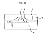
- FIG. 22 shows an exemplary configuration of a conventional piezoelectric oscillator (JP-U-1-82507).
- the piezoelectric oscillator is configured as follows.
- a semiconductor device 1 is fixed to one surface of a lead frame 5 with an adhesive or the like and a piezoelectric resonator 4 housed in a cylindrical package is fixed to the other surface of the lead frame 5.
- the semiconductor device 1 and the external terminals of the lead frame 5 are connected via bonding wires 3.
- the entire structure is molded with a resin 6.
- Such a structure can avoid various inconveniences occurring when the piezoelectric resonator element and the oscillation circuit are housed in the same package.
- the conventional piezoelectric oscillators when a frequency displacement of the piezoelectric resonator assumes problematic values after resin molding, no measure therefor has been taken. That is, in recent years, considerably high accuracy is required for the frequency performance of a piezoelectric oscillator. After the package of the piezoelectric resonator is sealed, when the frequency of the piezoelectric resonator changes to a problematic extent due to the influence of the subsequent manufacturing process or the like, it is impossible to ship the piezoelectric oscillator as a product. Further, the conventional piezoelectric oscillators have some problems. Specifically, the components are wasted, the manufacturing yield also decreases, and, consequently, the manufacturing cost increases.
- a piezoelectric oscillator according to the pre-characterizing portion of claim 1 is known from GB 2 055 232 A.
- An object of the present invention is to provide a piezoelectric oscillator having an exposed transparent lid of the resonator package that allows for fine adjustment of the frequency after resin molding, a manufacturing method therefor, and a mobile phone and an electronic apparatus using the piezoelectric oscillator.
- resin molding is performed such that the transparent lid of the resonator package is exposed to the outside. More particularly, deforming the lead frame as claimed facilitates avoiding resin to cover the transparent lid during the molding process.
- the island portion has holding lead portions that have a smaller width than the island portion and that extend outward, and the deformation is provided at the holding lead portions.
- the holding lead portions are formed to have a smaller width than the island portion, stress generated during the resin molding is readily concentrated at the holding lead portions. This allows the holding lead portions to be appropriately deformed while avoiding the deformation of the island portion associated with the fixing function of the lead frame with respect to the resonator package and the semiconductor device. Also, since stress generated from the deformation is concentrated at the holding lead portions, it is possible to prevent the semiconductor device from being damaged.
- portions of the holding lead portions have deformation portions for facilitating deformation. According to this configuration, when portions of the holding lead portions further have deformation portions for facilitating deformation, stress generated during the molding process can be appropriately concentrated at the deformation portions.
- the deformation portions can be provided by, for example, reducing the width of appropriate positions of the holding lead portions relative to the other regions.
- the deformation portions are defined by slits that penetrate the island portion at opposite sides of the holding lead portions. According to this configuration, since the deformation portions are defined by slits that penetrate the island portion at opposite sides of the holding lead portions, there is no need to reduce the width of the holding lead portions. Further, it is possible to concentrate stress at the slit formation regions while maintaining the component holding function during the molding process, and is also possible to facilitate the deformation of the deformation portions.
- the resonator package is fixed with at least three protrusion surfaces abutting against the island portion.
- the protrusion surfaces slightly protrude. According to this configuration, even when stress that causes the lead frame to be partly deformed is applied to the resonator package during the molding process, the resonator package can easily be positioned horizontally with respect to the island portion, since the resonator package abuts against the island portion at at least three protrusion surfaces. This arrangement, therefore, can effectively prevent the resonator package from being molded in a declined state.
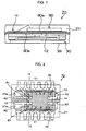
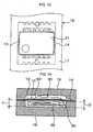
- FIGS. 1 and 2 show an embodiment of a piezoelectric oscillator of the present invention, FIG. 1 being a schematic sectional view thereof and FIG. 2 being a schematic plan view thereof.
- FIGS. 1 and 2 show the internal structure of a resin mold portion in a transparent manner for convenience of understanding.
- a piezoelectric oscillator 70 has a resonator package 30, in which a piezoelectric resonator element is housed, and an IC chip 80, which is a semiconductor device in which an oscillation circuit that is electrically connected to the resonator package 30 is incorporated.
- the oscillator 70 is constructed as follows.
- the IC chip 80 is fixed to one surface (the upper surface in FIG. 1) of a lead frame 10 and the resonator package 30 is fixed to the other surface (the lower surface in FIG. 1) of the lead frame 10.
- the resulting structure is molded with a resin 21 such that only a lid 39 of the resonator package 30 is exposed.
- the resonator package 30 incorporated in the oscillator 70 of the embodiment will first be described with reference to FIGS. 3 to 5.
- the resonator package 30 can be used alone as a piezoelectric device, and in the embodiment, FIGS. 3 and 4 particularly show an example in which the resonator package 30 is configured with a quartz crystal resonator.
- the resonator package 30 has a housing container (a ceramic container) 36 in which a piezoelectric resonator element 32 is housed.
- the housing container 36 is formed by depositing a plurality of substrates, each being formed by shaping a ceramic green sheet containing aluminum oxide as insulating material, and then sintering the substrates. Each substrate has a predetermined hole therein, so that, when stacked, the substrates define a predetermined internal space S2 therein.
- the internal space S2 serves as a housing space for housing the resonator element 32.
- the housing container 36 is formed by stacking a first multilayer substrate 61, a second multilayer substrate 64, and a third multilayer substrate 68 from the bottom.
- the second multilayer substrate 64 that is exposed to the internal space S2 and that defines the internal bottom portion has electrode portions 31, which are formed by, for example, plating a tungsten metallized member with nickel and gold.
- the electrode portions 31 provide external connections and supply drive voltages.
- Conductive adhesive 43 is applied to the electrode portions 31, a base 51 of the resonator element 32 is placed on the conductive adhesive 43, and the conductive adhesive 43 is cured.
- the conductive adhesive 43 an adhesive that contains conductive particles, such as silver fine particles, in a synthetic resin that serves as an adhesive component having a bonding capability can be used.
- a silicone, epoxy, polyimide conductive adhesive, or the like can be used.
- the resonator element 32 is formed by etching a piezoelectric material, for example, quartz crystal.
- the resonator element 32 is formed to have a small size and has a shape particularly shown in FIG. 3 to provide necessary performance.
- the resonator element 32 has the base 51, which is fixed to the housing container 36, and a pair of resonating arms 34 and 35, which bifurcate from the base 51 and extend in parallel to each other toward the right side in the figure.
- a so-called "tuning-fork type resonator element" which has the overall shape of a turning fork, is used as the resonator element 32.
- the resonating arms 34 and 35 of the resonator element 32 have corresponding elongated grooves 56 and 57, which have bottoms and which extend in the longitudinal direction. As shown in FIG. 5, which is a cross-sectional view taken along line C-C shown in FIG. 3, the grooves 56 and 57 are provided in both obverse and reverse surfaces of the corresponding resonating arms 34 and 35.
- extraction electrodes 52 and 53 are provided in the vicinity of two opposite ends in the lateral direction at an end portion (the left end portion in FIG. 3) of the base 51 of the resonator element 32. Similarly, the extraction electrodes 52 and 53 are formed on the reverse surface, not shown, of the base 51 of the resonator element 32.
- the extraction electrodes 52 and 53 are portions that are connected to the electrode portions 31 in the housing container 36 shown in FIG. 3 with the conductive adhesive 43, as described above.
- the electrode portions 31 are connected to corresponding mounting terminals 31 a provided on an outer surface of the left end portion of the first multilayer substrate 61.
- the mounting terminals 31a are provided at two opposite ends in the lateral direction of the resonator package 30.
- dummy electrodes 31b are provided on an outer surface of the right end portion of the first multilayer substrate 61.
- the dummy electrodes 31 b are not connected to the resonator element 32 and have the same shape as the mounting terminals 31a.
- the dummy electrodes 31b are provided at two opposite ends in the lateral direction at the right end portion of the first multilayer substrate 61.
- the extraction electrodes 52 and 53 of the resonator element 32 are connected to corresponding excitation electrodes 54 and 55 (not shown) provided in the grooves 56 and 57 of the resonating arms 34 and 35.
- the excitation electrodes 54 and 55 are also formed at two opposite side surfaces of the corresponding resonating arms 34 and 35.
- the excitation electrodes 54 in the grooves 57 and the excitation electrodes 55 on its side surface portions are adapted to have opposite polarities to each other.
- the excitation electrodes 55 in the grooves 56 and the excitation electrodes 54 on its side surface portions are adapted to have opposite polarities to each other.
- the through-hole 37 is shaped to have a stepped opening with a downward step portion 62 in FIG. 4.
- a metal coating portion is preferably provided on the surface of the step portion 62.
- the through-hole 37 is filled with a metal sealant 38, which is preferably selected from, for example, lead-free sealants, and is selected from, for example, a silver brazing material, Au/Sn alloy, and Au/Ge alloy.
- the metal coating portion on the surface of the step portion 62 is preferably formed by plating a tungsten metallized member with nickel and gold.
- the lid 39 is joined to the open upper end of the housing container 36 with a brazing material 36a, such as a low-melting-point glass, to seal the housing container 36.
- the lid 39 is formed of a light transparent material, particularly, thin-plate glass, so that metal coating portions (described below) of the resonator element 32 can be illuminated with external laser light L2, as described below, to allow the frequency to be changed by a mass reduction technique.
- a suitable material for making the lid 39 transparent is generally glass.
- a thin-plate glass e.g., borosilicate glass, manufactured by down drawing is used.
- the mounting terminals 31a, the dummy terminals 31b, and the metal sealant 38 provide protrusion portions that slightly protrude at the bottom surface of the first substrate 61 to such a degree corresponding to the thickness of the electrodes.
- the amount of protrusion of the mounting terminals 31a, the dummy terminals 31b, and the metal sealant 38 is substantially the same.
- a recess 42 is provided by removing a portion of the second substrate 64. Consequently, in a case in which the resonator package 30 is externally shocked, even when the tips of the resonator element 32 are displaced in the arrow D direction, the tips of the resonator element 32 do not hit the inner bottom portion of the housing container 36, thereby effectively preventing the resonator element 32 from being damaged.
- Constricted portions or notches 44 and 45 are preferably formed in the vicinity of base portions of the resonating arms 34 and 35 in the base 51 of the resonator element 32. These constricted portions or notches 44 and 45 are inwardly notched at two opposite edges of the base 51 in the lateral direction. This can effectively prevent the flexural vibrations of the resonating arms 34 and 35 from leaking toward the base 51.
- the IC chip 80 which is a semiconductor device, houses an oscillation circuit formed of an integrated circuit, which is not shown.
- the IC chip 80 is fixed to one surface of an island portion, described below, of the lead frame 10 by using, for example, an epoxy or silicon adhesive 80a.
- one surface of the IC chip 80 is provided with a plurality of terminal portions. These terminal portions are connected to corresponding inner leads of external terminal portions 11 (described below) of the lead frame 10 by wire bonding.
- the number of terminal portions of the IC chip 80 may be larger or smaller than the number of terminal portions shown in FIG. 2, depending on the type of the IC chip.
- the terminal portions 81 of the IC chip 80 in the embodiment are called, for example, gate/drain (G/D) terminals, and serve as terminals for connection with the resonator package 30.
- the terminal portions 81 are connected using bonding wires 82 to the above-described mounting terminals 31 a of the resonator package 30.
- they are not interconnected via the lead frame 10. This offers an advantage in that the stray capacitance does not increase between the terminals. Since individual configurations of other terminal portions of the IC chip 80 are different from each other depending on the type of the IC chip 80, the descriptions thereof are omitted.
- the oscillator 70 of the embodiment is configured as described below, and is molded with the resin in a manufacturing process described above such that the transparent lid 39 of the resonator package 30 is exposed to the outside, as shown in FIG. 1.
- the inside of the oscillator 70 can be illuminated with external laser light L2 for frequency adjustment through the transparent lid 39, by the same method as that described with reference to FIG. 4.
- the frequency of the resonator element 32 within the resonator package 30 can be adjusted.
- the electrodes of the resonator element 32 can be partly vaporized with the laser light L2 by a mass reduction technique, so that the frequency can be adjusted.
- the resonator package 30 is arranged at the lower side (the mounting substrate side) and the IC chip 80 is arranged at the upper side so as to sandwich the lead frame 10 therebetween.
- the arrangement may be such that the resonator package 30 is arranged at the upper side and the IC chip 80 is arranged at the lower side (the mounting substrate side) so as to sandwich the lead frame 10, so that the lid 39 is exposed upward.
- the external terminal portions 11 are formed to have a so-called "J-lead" shape in which terminals 11a are bent downward (toward the mounting substrate) so as to go around the resin 21.
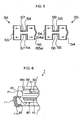
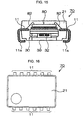
- FIG. 7 is a flow chart of a preferred embodiment of a manufacturing method for the oscillator 70 of the embodiment.
- FIG. 8 is a schematic plan view showing the configuration of a lead frame prepared for the manufacture of the oscillator 70.
- the lead frame 10 one that is commonly used for manufacturing a package device can be used.
- Examples include a lead frame formed of an Fe alloy, such as a 42 alloy; a Cu metal, such as Cu-Sn, Cu-Fe, Cu-Zn, or Cu-Ni; or ternary alloy containing a third element added to those alloys.
- the lead frame 10 has an outer frame portion 17, an island portion 12, and the external terminal portions 11.
- the island portion 12 is provided inside the outer frame portion 17 and in the vicinity of substantially the center thereof to serve as a die pad.
- the external terminal portions 11 are arranged to be parallel to each other at two opposite sides of the island portion 12 in the lateral direction to serve as lead portions. Further, the external terminal portions 11 are separated from the island portion 12 and are supported by the outer frame portion 17.
- the number of external terminal portions 11 is determined so as to correspond to, for example, the number of terminals of the IC chip 80 which are to be connected to the external terminal portions 11.
- the island portion 12 serves as a die pad for mounting a device and has an area and a width which are suitable for that purpose.
- the island portion 12 has holding lead portions 13 and 14 that integrally extend from two opposite edges of the island portion 12.
- the holding lead portions 13 and 14 have a width that is smaller than the width of the island portion 12, extend toward the outer frame portion 17, and are integrated with the outer frame portion 17.
- the island portion 12 has a structure in which it is supported with respect to the outer frame portion 17 of the lead frame 10 by the narrow holding lead portions 13 and 14.
- the island portion 12 is formed to have slits 15 and slits 16, which are formed so as to penetrate the island portion 12 at two opposite sides in the lateral direction of the holding lead portions 13 and 14, as shown in FIG. 8. That is, the slits 15 and the slits 16 are provided as one variation of a deformation portion for facilitating the deformation of the holding lead portions 13 and 14 in a manufacturing process described below.
- the deformation portions may be notch portions that are formed by notching a larger area of the island portion 12.
- predetermined portions of the holding lead portions 13 and 14 may be set to have a smaller width than the other regions.
- the deformation portions can be provided by forming structurally weak portions at the holding lead portions 13 and 14 or the portion where the holding lead portions 13 and 14 and the island portion 12 are integrated with each other so that stress generated in a molding process described below is concentrated at that portion.
- the island portion 12 may be provided with a deformation portion by forming the island portion 12 such it has an irregular shape itself, to allow a portion of the island portion 12 to be deformed.
- step ST1 of FIG. 7 the IC chip 80 is bonded as shown in FIG. 9(a) using the lead frame 10 illustrated in FIG. 8.
- one surface of the IC chip 80 is bonded to the island portion 12 of the lead frame 10 using the adhesive illustrated in FIG. 1.
- FIG. 9(b) shows a surface opposite to the surface shown in FIG. 9(a).
- the resonator package 30 is bonded to the island portion 12 using, for example, an epoxy or silicon adhesive (step ST2).
- the adhesive is indicated by reference numeral 30a in FIG. 1.
- the mounting terminals 31 a of the resonator package 30 are bonded and fixed so as to be exposed from the island portion 12.
- the dummy terminals 31 b which are arranged at two opposite end portions in the lateral direction at the end portions in the lateral direction of the resonator package 30, and the metal sealant 38, which is provided in the vicinity of the center of the resonator package 30, abut against the bottom surface of the resonator package 30 (see FIG. 9(b)).
- the resonator package 30 abuts against the island portion 12 at the three points. Thus, the resonator package 30 is fixed without inclination relative to the island portion 12.
- the individual terminals of the IC chip 80 and the corresponding inner leads of the external terminal portions 11 are connected by wire bonding (step ST3 in FIG. 7).
- the gate/drain (G/D) terminals which are the terminal portions 81 of the IC chip 80, are connected to the above-described mounting terminals 31a, which are exposed from the island portion 12 of the resonator package 30, by using the bonding wires 82, such as gold (Au) lines.
- the bonding wires 82 are covered with a resin mold described below, so that the terminal portions 81 of the IC chip 80 and their conductive portions are not exposed to the outside. This can prevent moisture in the air from attaching to those portions and thus can prevent short-circuiting.
- electrical connections are provided between the lead frame 10 and the IC chip 80 and between the IC chip 80 and the resonator package 30.
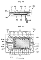
- step ST4 in FIG. 7 resin molding is performed (step ST4 in FIG. 7).
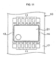
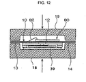
- first and second molding dies 18 and 19 are used as shown in FIGS. 11 and 12.
- the first die 18 is shown at the lower side in FIGS. 12 and 14 and the second die 19 is shown at the upper side in FIGS. 12 and 14.
- the first die 18 and/or the second die 19 are moved relative to each other in the arrow directions as shown in FIG. 12, so that the periphery of the island portion 12 of the lead frame 10 is sandwiched between the dies 18 and 19.
- the resonator package 30 and the IC chip 80 which is fixed to the island portion 12, are housed in the dies and molten resin is injected into the combined dies through a gate, which is not shown, so that a mold is provided by transfer molding.
- a gate which is not shown, so that a mold is provided by transfer molding.
- an epoxy resin can be used for the molding resin.
- the first die 18 located below is set to have a depth D that is smaller than a thickness h including the lid 39 of the resonator package 30.
- the resonator package 30 and the IC chip 80 which is fixed to the island portion 12, are housed between the first die 18 and the second die 19 and are sandwiched therebetween with reference to the positions of the holding lead portions 13 and 14. That is, they are sandwiched such that the seam of the first die 18 and the second die 19 are set at the positions of the holding lead portions 13 and 14.
- the resonator package 30 is arranged such that the lid 39 abuts against an inner surface of the first die 18 in the dies.
- the depth D of the first die 18 is designed to be smaller than the thickness h including the lid 39 of the resonator package 30, the outer surface of the lid 39 is pressed strongly against the inner surface of the first die 18 and the holding lead portions 13 and 14 are deformed as shown. That is, the holding lead portions 13 and 14 adjacent to the island portion 12 are deformed upward.
- a plane in which the external terminal portions 11 that have the plurality of leads, which constitute the external terminals, are located, and a plane in which the island portion 12 exists are at different positions from each other.
- the resonator package 30 is deformed upward in the figure and the outer surface of the lid 39 is strongly pressed against the inner surface of the first die 18.
- molten resin is injected into the dies, so that the molten resin surrounds the IC chip 80, which is fixed to the island portion 12, and the resonator package 30, except for the outer surface of the lid 39.
- this arrangement prevents the resin from entering between the outer surface of the lid 39 and the inner surface of the first die 18.
- This arrangement also prevents the resin from becoming burrs and attaching to the outer surface of the lid 39 after the molding.
- connections with the outer frame portion 17 are disconnected except for the holding lead portions 13 and 14. That is, the outer edge portions of the external terminal portions 11 are cut (step ST4 in FIG. 7).
- step ST5 in FIG. 7 portions exposed from the cut external terminal portions 11 are subjected to terminal plating.
- step ST6 in FIG. 7 portions exposed from the cut external terminal portions 11 are subjected to terminal plating.
- the electrode portions of the resonator element 32 are illuminated with external laser light L2 through the transparent lid 39 that is exposed to the outside.
- the metal coating portions of the electrode portions can be partly vaporized, so that the frequency can be adjusted to be higher by a mass reduction technique (step ST7 in FIG. 7).
- step ST8 in FIG. 7 the structure is subjected to the necessary inspection (step ST8 in FIG. 7) to thereby provide the completed oscillator 70.
- FIG. 18 is a schematic plan view showing a first modification of the embodiment of the oscillator according to the present invention. Portions denoted with the same reference numerals as those used in the description of the oscillator 70 have common structures, and thus duplicated descriptions are omitted. Now, differences will be mainly described.
- a piezoelectric oscillator 70-1 of the first modification is different in the structure of the island portion from the above-described oscillator 70.
- an island portion 12-1 does not have the slits 15 but has a substantially rectangular plate shape.
- stress generated when the dies are clamped is concentrated at the holding lead portions 13 and 14 that have a width smaller than the width of the island portion 12-1.
- the holding lead portions 13 and 14 serve as deformation portions to prevent an event in which undue stress applied to the IC chip 80 and so on causes damage.
- the shape of the island portion 12-1 is simple, which facilitates the manufacture and also improves the strength correspondingly.
- FIGS. 19 and 20 show other modifications of the embodiment of the piezoelectric oscillator of the present invention.
- FIG. 19 is a schematic sectional view in the lateral direction of a piezoelectric oscillator 70-2 according to a second modification
- FIG. 20 is a schematic sectional view in the lateral direction of a piezoelectric oscillator 70-3 according to a third embodiment.
- FIG. 20 illustrates only the left side since the right and left sections thereof are substantially symmetrical.
- the oscillator 70-2 of the second modification and the oscillator 70-3 of the third modification are different from each other in the bending direction and the bending form of the external terminal portions 11.
- the vicinity of the base portions of the external terminal portions 11 is bent in an opposite direction to that in the oscillator 70, i.e., bent toward the IC chip 80, and tip portions 11b are bent in the horizontal direction.
- the vicinity of the base portions of the external terminal portions 11 is bent toward the mounting substrate, not shown, (i.e., toward the lower side in FIG. 20) and center portions 11c are bent in the horizontal direction and are exposed to the outside. Further, tip portions 11d of the external terminal portions 11 are bent toward the resonator package 30 (i.e., toward the upper side in FIG. 20) and are exposed to the outside so as to lie along side surfaces of the resin 21.
- the oscillators 70-2 and 70-3 of the modifications of the present invention can be configured to have different forms of external terminals so as to correspond to, for example, mounting conditions for the substrate.
- FIG. 21 is a diagram showing a schematic configuration of a digital mobile phone apparatus, which is one example of an electronic apparatus using the piezoelectric oscillator according to the present invention.
- a sender's voice is converted by a microphone 308 into an electrical signal, which is then modulated by a demodulator/codec unit into a digital signal.
- the digital signal is converted by a transmitting unit 307 to an RF (radio frequency) band and the resulting RF signal is transmitted to a base station (not shown) via an antenna.
- the frequency of an RF signal transmitted from a base station is converted by a receiving unit 306.
- the resulting signal is converted by the demodulator/codec unit into an audio signal, which is then output from a speaker 309.
- a CPU (central processing unit) 301 controls the entire operation of the digital mobile phone apparatus 300, including an input/output section 302 constituted by a liquid crystal display device and a keyboard.
- a memory 303 is information storing means, which is implemented by RAM, ROM, and the like, and is controlled by the CPU 301.
- the memory 303 stores, for example, telephone-book information and a control program for the digital mobile phone apparatus 300.
- the piezoelectric oscillator according to the present invention can be applied to, for example, a TCXO (Temperature Compensated X'tal Oscillator) 305.
- This TCXO 305 is a piezoelectric oscillator having a small frequency fluctuation with respect to a change in ambient temperature, and is widely applied to mobile phone apparatuses as a frequency reference source for the receiving unit 306 and the transmitting unit 307 shown in FIG. 21.
- TCXO 305 having the structure according to the embodiment of the present invention is very useful for the miniaturization.
- the piezoelectric oscillator as described above when used for an electronic apparatus, such as the digital mobile phone apparatus 300, fine adjustment of the frequency can be achieved even after the resin molding.
- This arrangement therefore, can improve the manufacturing yield and can reduce the manufacturing cost.
- the arrangement can also reduce the manufacturing cost of electronic apparatuses, such as the digital mobile phone apparatus 300.
Landscapes
- Physics & Mathematics (AREA)
- Acoustics & Sound (AREA)
- Chemical & Material Sciences (AREA)
- Crystallography & Structural Chemistry (AREA)
- Oscillators With Electromechanical Resonators (AREA)
- Piezo-Electric Or Mechanical Vibrators, Or Delay Or Filter Circuits (AREA)
Description
- The present invention relates to a piezoelectric oscillator having a piezoelectric resonator package housing a piezoelectric resonator element and a semiconductor device including an oscillation circuit for oscillating the piezoelectric resonator element, a manufacturing method for the piezoelectric oscillator, and a mobile phone and an electronic apparatus using the piezoelectric oscillator.
- Piezoelectric oscillators have been widely used in packages for HDDs (hard disk drives), mobile computers, compact information apparatuses, such as IC cards and mobile communication apparatuses, such as mobile phones, automobile phones, and paging systems.
- FIG. 22 shows an exemplary configuration of a conventional piezoelectric oscillator (JP-U-1-82507). In the figure, the piezoelectric oscillator is configured as follows. A
semiconductor device 1 is fixed to one surface of alead frame 5 with an adhesive or the like and apiezoelectric resonator 4 housed in a cylindrical package is fixed to the other surface of thelead frame 5. Thesemiconductor device 1 and the external terminals of thelead frame 5 are connected viabonding wires 3. The entire structure is molded with aresin 6. - Such a structure can avoid various inconveniences occurring when the piezoelectric resonator element and the oscillation circuit are housed in the same package.
- That is, when the piezoelectric resonator element and the oscillation circuit are simultaneously housed in a resin package, gas generated when the resin is cured may attach to the piezoelectric resonator element, thus leading to a decline in performance. Accordingly, as described above, when the piezoelectric resonator element and the oscillation circuit are housed in the separate packages and are fixed to different surfaces of the lead frame, those inconveniences can be avoided and the configuration can be miniaturized. Such a configuration is also disclosed in JP-A-7-162236.
- However, with the conventional piezoelectric oscillators, when a frequency displacement of the piezoelectric resonator assumes problematic values after resin molding, no measure therefor has been taken. That is, in recent years, considerably high accuracy is required for the frequency performance of a piezoelectric oscillator. After the package of the piezoelectric resonator is sealed, when the frequency of the piezoelectric resonator changes to a problematic extent due to the influence of the subsequent manufacturing process or the like, it is impossible to ship the piezoelectric oscillator as a product. Further, the conventional piezoelectric oscillators have some problems. Specifically, the components are wasted, the manufacturing yield also decreases, and, consequently, the manufacturing cost increases.
- A piezoelectric oscillator according to the pre-characterizing portion of
claim 1 is known from GB 2 055 232 A. - An object of the present invention is to provide a piezoelectric oscillator having an exposed transparent lid of the resonator package that allows for fine adjustment of the frequency after resin molding, a manufacturing method therefor, and a mobile phone and an electronic apparatus using the piezoelectric oscillator.
- This object is achieved by a piezoelectric oscillator as claimed in
claim 1 and a method of manufacturing it as claimed inclaim 6. Preferred embodiments an uses of the invention are subject-matter of the dependent claims. - According to the invention, resin molding is performed such that the transparent lid of the resonator package is exposed to the outside. More particularly, deforming the lead frame as claimed facilitates avoiding resin to cover the transparent lid during the molding process.
- In an embodiment of the present invention, the island portion has holding lead portions that have a smaller width than the island portion and that extend outward, and the deformation is provided at the holding lead portions. According to this configuration, since the holding lead portions are formed to have a smaller width than the island portion, stress generated during the resin molding is readily concentrated at the holding lead portions. This allows the holding lead portions to be appropriately deformed while avoiding the deformation of the island portion associated with the fixing function of the lead frame with respect to the resonator package and the semiconductor device. Also, since stress generated from the deformation is concentrated at the holding lead portions, it is possible to prevent the semiconductor device from being damaged.
- In an embodiment of the present invention, portions of the holding lead portions have deformation portions for facilitating deformation. According to this configuration, when portions of the holding lead portions further have deformation portions for facilitating deformation, stress generated during the molding process can be appropriately concentrated at the deformation portions. The deformation portions can be provided by, for example, reducing the width of appropriate positions of the holding lead portions relative to the other regions.
- In an embodiment of the present invention, the deformation portions are defined by slits that penetrate the island portion at opposite sides of the holding lead portions. According to this configuration, since the deformation portions are defined by slits that penetrate the island portion at opposite sides of the holding lead portions, there is no need to reduce the width of the holding lead portions. Further, it is possible to concentrate stress at the slit formation regions while maintaining the component holding function during the molding process, and is also possible to facilitate the deformation of the deformation portions.
- In an embodiment of the present invention, the resonator package is fixed with at least three protrusion surfaces abutting against the island portion. The protrusion surfaces slightly protrude. According to this configuration, even when stress that causes the lead frame to be partly deformed is applied to the resonator package during the molding process, the resonator package can easily be positioned horizontally with respect to the island portion, since the resonator package abuts against the island portion at at least three protrusion surfaces. This arrangement, therefore, can effectively prevent the resonator package from being molded in a declined state.
Preferred embodiments of the invention will be described in detail below with reference to the drawings, in which: - FIG. 1
- is a schematic sectional view showing an embodiment of a piezoelectric oscillator of the present invention;
- FIG. 2
- is a schematic plan view of the oscillator shown in FIG. 1;
- FIG. 3
- is a schematic plan view of a resonator package used for the oscillator shown in FIG. 1;
- FIG. 4
- is a schematic sectional view taken along line B-B shown in FIG. 3;
- FIG. 5
- is a schematic sectional view taken along line C-C shown in FIG. 3;
- FIG. 6
- is a schematic cross sectional view of a structure in which the oscillator shown in FIG. 1 is modified;
- FIG. 7
- is a flow chart showing a brief overview of an example of a manufacturing process of the oscillator shown in FIG. 1;
- FIG. 8
- is a schematic plan view showing one example of a lead frame prepared in the manufacturing process shown in FIG. 7;
- FIGS. 9(a) and 9(b)
- show a schematic views illustrating a part of the manufacturing process shown in FIG. 7, FIG. 9(a) being a schematic plan view and FIG. 9(b) being a schematic bottom view;
- FIG. 10
- is a schematic plan view illustrating a part of the manufacturing process shown in FIG. 7;
- FIG. 11
- is a schematic plan view illustrating a part of the manufacturing process shown in FIG. 7;
- FIG. 12
- is a schematic sectional view showing a state before the dies are clamped in the process shown in FIG. 11;
- FIG. 13
- is a schematic plan view illustrating a part of the manufacturing process shown in FIG. 7;
- FIG. 14
- is a schematic sectional view showing a state after the dies are clamped in the process shown in FIG. 13;
- FIG. 15
- is a schematic plan view illustrating a part of the manufacturing process shown in FIG. 7;
- FIG. 16
- is a schematic plan view illustrating the completed form of the oscillator shown in FIG. 1;
- FIG. 17
- is a schematic sectional view illustrating a frequency adjustment process in the manufacturing process shown in FIG. 7;
- FIG. 18
- is a schematic plan view illustrating a first modification of the oscillator shown in FIG. 1;
- FIG. 19
- is a schematic sectional view illustrating a second modification of the oscillator shown in FIG. 1;
- FIG. 20
- is a schematic cross sectional view showing a third modification of the oscillator shown in FIG. 1;
- FIG. 21
- is a diagram showing a schematic configuration of a digital mobile phone apparatus, which is one example of an electronic apparatus using the piezoelectric oscillator according to the present invention; and
- FIG. 22
- is a schematic sectional view showing an example of a conventional piezoelectric oscillator.
- FIGS. 1 and 2 show an embodiment of a piezoelectric oscillator of the present invention, FIG. 1 being a schematic sectional view thereof and FIG. 2 being a schematic plan view thereof. FIGS. 1 and 2 show the internal structure of a resin mold portion in a transparent manner for convenience of understanding.
- In the figures, a
piezoelectric oscillator 70 has aresonator package 30, in which a piezoelectric resonator element is housed, and anIC chip 80, which is a semiconductor device in which an oscillation circuit that is electrically connected to theresonator package 30 is incorporated. - More specifically, the
oscillator 70 is constructed as follows. TheIC chip 80 is fixed to one surface (the upper surface in FIG. 1) of alead frame 10 and theresonator package 30 is fixed to the other surface (the lower surface in FIG. 1) of thelead frame 10. The resulting structure is molded with aresin 21 such that only alid 39 of theresonator package 30 is exposed. - The
resonator package 30 incorporated in theoscillator 70 of the embodiment will first be described with reference to FIGS. 3 to 5. - The
resonator package 30 can be used alone as a piezoelectric device, and in the embodiment, FIGS. 3 and 4 particularly show an example in which theresonator package 30 is configured with a quartz crystal resonator. Theresonator package 30 has a housing container (a ceramic container) 36 in which apiezoelectric resonator element 32 is housed. Thehousing container 36 is formed by depositing a plurality of substrates, each being formed by shaping a ceramic green sheet containing aluminum oxide as insulating material, and then sintering the substrates. Each substrate has a predetermined hole therein, so that, when stacked, the substrates define a predetermined internal space S2 therein. - The internal space S2 serves as a housing space for housing the
resonator element 32. - That is, as shown in FIG. 4, in the embodiment, the
housing container 36 is formed by stacking afirst multilayer substrate 61, asecond multilayer substrate 64, and athird multilayer substrate 68 from the bottom. - In the figure, in the vicinity of left end portions in the internal space S2 of the
housing container 36, thesecond multilayer substrate 64 that is exposed to the internal space S2 and that defines the internal bottom portion haselectrode portions 31, which are formed by, for example, plating a tungsten metallized member with nickel and gold. - The
electrode portions 31 provide external connections and supply drive voltages.Conductive adhesive 43 is applied to theelectrode portions 31, abase 51 of theresonator element 32 is placed on theconductive adhesive 43, and theconductive adhesive 43 is cured. As theconductive adhesive 43, an adhesive that contains conductive particles, such as silver fine particles, in a synthetic resin that serves as an adhesive component having a bonding capability can be used. Alternatively, a silicone, epoxy, polyimide conductive adhesive, or the like can be used. - The
resonator element 32 is formed by etching a piezoelectric material, for example, quartz crystal. In this embodiment, theresonator element 32 is formed to have a small size and has a shape particularly shown in FIG. 3 to provide necessary performance. - That is, the
resonator element 32 has thebase 51, which is fixed to thehousing container 36, and a pair of resonatingarms base 51 and extend in parallel to each other toward the right side in the figure. Thus, a so-called "tuning-fork type resonator element", which has the overall shape of a turning fork, is used as theresonator element 32. - The resonating
arms resonator element 32 have corresponding elongatedgrooves grooves arms - Referring to FIG. 3,
extraction electrodes base 51 of theresonator element 32. Similarly, theextraction electrodes base 51 of theresonator element 32. - The
extraction electrodes electrode portions 31 in thehousing container 36 shown in FIG. 3 with theconductive adhesive 43, as described above. Theelectrode portions 31 are connected to corresponding mountingterminals 31 a provided on an outer surface of the left end portion of thefirst multilayer substrate 61. In practice, the mountingterminals 31a are provided at two opposite ends in the lateral direction of theresonator package 30. Further,dummy electrodes 31b are provided on an outer surface of the right end portion of thefirst multilayer substrate 61. Thedummy electrodes 31 b are not connected to theresonator element 32 and have the same shape as the mountingterminals 31a. Thedummy electrodes 31b are provided at two opposite ends in the lateral direction at the right end portion of thefirst multilayer substrate 61. - The
extraction electrodes resonator element 32 are connected to correspondingexcitation electrodes 54 and 55 (not shown) provided in thegrooves arms excitation electrodes arms arm 34, theexcitation electrodes 54 in thegrooves 57 and theexcitation electrodes 55 on its side surface portions are adapted to have opposite polarities to each other. With regard to the resonatingarm 35, theexcitation electrodes 55 in thegrooves 56 and theexcitation electrodes 54 on its side surface portions are adapted to have opposite polarities to each other. - As shown in FIG. 4, in the vicinity of substantially the center of the bottom surface of the
housing container 36, interconnected through-holes multilayer substrates housing container 36, so that a through-hole 37 that is open to the outside is provided. Of the two through-holes constituting the through-hole 37, the outer through-hole 37a, which is a second hole located outside, has a larger inner diameter than thefirst hole 37b, which opens to the inside of theresonator package 30. Thus, the through-hole 37 is shaped to have a stepped opening with adownward step portion 62 in FIG. 4. A metal coating portion is preferably provided on the surface of thestep portion 62. - The through-
hole 37 is filled with ametal sealant 38, which is preferably selected from, for example, lead-free sealants, and is selected from, for example, a silver brazing material, Au/Sn alloy, and Au/Ge alloy. Correspondingly, the metal coating portion on the surface of thestep portion 62 is preferably formed by plating a tungsten metallized member with nickel and gold. - The
lid 39 is joined to the open upper end of thehousing container 36 with abrazing material 36a, such as a low-melting-point glass, to seal thehousing container 36. Thelid 39 is formed of a light transparent material, particularly, thin-plate glass, so that metal coating portions (described below) of theresonator element 32 can be illuminated with external laser light L2, as described below, to allow the frequency to be changed by a mass reduction technique. - A suitable material for making the
lid 39 transparent is generally glass. As such glass material, a thin-plate glass, e.g., borosilicate glass, manufactured by down drawing is used. - With this structure, as shown in FIG. 4, the mounting
terminals 31a, thedummy terminals 31b, and themetal sealant 38 provide protrusion portions that slightly protrude at the bottom surface of thefirst substrate 61 to such a degree corresponding to the thickness of the electrodes. The amount of protrusion of the mountingterminals 31a, thedummy terminals 31b, and themetal sealant 38 is substantially the same. - Further, referring to FIG. 4, a
recess 42 is provided by removing a portion of thesecond substrate 64. Consequently, in a case in which theresonator package 30 is externally shocked, even when the tips of theresonator element 32 are displaced in the arrow D direction, the tips of theresonator element 32 do not hit the inner bottom portion of thehousing container 36, thereby effectively preventing theresonator element 32 from being damaged. - Constricted portions or
notches arms base 51 of theresonator element 32. These constricted portions ornotches arms base 51. - Next, referring to FIG. 1, the
IC chip 80, which is a semiconductor device, houses an oscillation circuit formed of an integrated circuit, which is not shown. TheIC chip 80 is fixed to one surface of an island portion, described below, of thelead frame 10 by using, for example, an epoxy or silicon adhesive 80a. - As shown in FIG. 2, one surface of the
IC chip 80, the surface being opposite to the surface joined to thelead frame 10, is provided with a plurality of terminal portions. These terminal portions are connected to corresponding inner leads of external terminal portions 11 (described below) of thelead frame 10 by wire bonding. Naturally, the number of terminal portions of theIC chip 80 may be larger or smaller than the number of terminal portions shown in FIG. 2, depending on the type of the IC chip. - Referring to FIG. 2, the
terminal portions 81 of theIC chip 80 in the embodiment are called, for example, gate/drain (G/D) terminals, and serve as terminals for connection with theresonator package 30. Theterminal portions 81 are connected usingbonding wires 82 to the above-describedmounting terminals 31 a of theresonator package 30. Thus, with regard to the electrical connection between theresonator package 30 and theIC chip 80, they are not interconnected via thelead frame 10. This offers an advantage in that the stray capacitance does not increase between the terminals. Since individual configurations of other terminal portions of theIC chip 80 are different from each other depending on the type of theIC chip 80, the descriptions thereof are omitted. - The
oscillator 70 of the embodiment is configured as described below, and is molded with the resin in a manufacturing process described above such that thetransparent lid 39 of theresonator package 30 is exposed to the outside, as shown in FIG. 1. Thus, after assembly, the inside of theoscillator 70 can be illuminated with external laser light L2 for frequency adjustment through thetransparent lid 39, by the same method as that described with reference to FIG. 4. As a result, after manufacture of theoscillator 70, particularly, after resin molding, the frequency of theresonator element 32 within theresonator package 30 can be adjusted. - That is, after the
lid 39 of theresonator package 30 is sealed, when the influence of the manufacturing process, such as resin molding, causes the frequency of theresonator element 32 to be changed to a problematic extent, for example, the electrodes of theresonator element 32 can be partly vaporized with the laser light L2 by a mass reduction technique, so that the frequency can be adjusted. - Additionally, not only can the frequency be adjusted but also unwanted wires and the like within the package can be disconnected after products are manufactured.
- In the above-described embodiment, the
resonator package 30 is arranged at the lower side (the mounting substrate side) and theIC chip 80 is arranged at the upper side so as to sandwich thelead frame 10 therebetween. Alternatively, as shown in FIG. 6, the arrangement may be such that theresonator package 30 is arranged at the upper side and theIC chip 80 is arranged at the lower side (the mounting substrate side) so as to sandwich thelead frame 10, so that thelid 39 is exposed upward. In this case, the externalterminal portions 11 are formed to have a so-called "J-lead" shape in whichterminals 11a are bent downward (toward the mounting substrate) so as to go around theresin 21. - FIG. 7 is a flow chart of a preferred embodiment of a manufacturing method for the
oscillator 70 of the embodiment. FIG. 8 is a schematic plan view showing the configuration of a lead frame prepared for the manufacture of theoscillator 70. - Before describing the manufacturing method for the
oscillator 70, the structure of a lead frame will first be described with reference to FIG. 8. - Referring to FIG. 8, for the
lead frame 10, one that is commonly used for manufacturing a package device can be used. Examples include a lead frame formed of an Fe alloy, such as a 42 alloy; a Cu metal, such as Cu-Sn, Cu-Fe, Cu-Zn, or Cu-Ni; or ternary alloy containing a third element added to those alloys. - The
lead frame 10 has anouter frame portion 17, anisland portion 12, and the externalterminal portions 11. Theisland portion 12 is provided inside theouter frame portion 17 and in the vicinity of substantially the center thereof to serve as a die pad. The externalterminal portions 11 are arranged to be parallel to each other at two opposite sides of theisland portion 12 in the lateral direction to serve as lead portions. Further, the externalterminal portions 11 are separated from theisland portion 12 and are supported by theouter frame portion 17. The number of externalterminal portions 11 is determined so as to correspond to, for example, the number of terminals of theIC chip 80 which are to be connected to the externalterminal portions 11. - The
island portion 12 serves as a die pad for mounting a device and has an area and a width which are suitable for that purpose. Theisland portion 12 has holdinglead portions island portion 12. The holdinglead portions island portion 12, extend toward theouter frame portion 17, and are integrated with theouter frame portion 17. Thus, theisland portion 12 has a structure in which it is supported with respect to theouter frame portion 17 of thelead frame 10 by the narrow holdinglead portions - Preferably, the
island portion 12 is formed to haveslits 15 and slits 16, which are formed so as to penetrate theisland portion 12 at two opposite sides in the lateral direction of the holdinglead portions slits 15 and theslits 16 are provided as one variation of a deformation portion for facilitating the deformation of the holdinglead portions island portion 12. Alternatively, predetermined portions of the holdinglead portions lead portions lead portions island portion 12 are integrated with each other so that stress generated in a molding process described below is concentrated at that portion. - Alternatively, the
island portion 12 may be provided with a deformation portion by forming theisland portion 12 such it has an irregular shape itself, to allow a portion of theisland portion 12 to be deformed. - An embodiment of a manufacturing method for the
oscillator 70 will now be described. - As shown in step ST1 of FIG. 7, the
IC chip 80 is bonded as shown in FIG. 9(a) using thelead frame 10 illustrated in FIG. 8. - That is, one surface of the
IC chip 80, the one surface being not the surface having the terminals of theIC chip 80, is bonded to theisland portion 12 of thelead frame 10 using the adhesive illustrated in FIG. 1. - FIG. 9(b) shows a surface opposite to the surface shown in FIG. 9(a). Next, as shown in FIG. 9(b), the
resonator package 30 is bonded to theisland portion 12 using, for example, an epoxy or silicon adhesive (step ST2). The adhesive is indicated byreference numeral 30a in FIG. 1. In this case, as shown in FIG. 9(a), the mountingterminals 31 a of theresonator package 30 are bonded and fixed so as to be exposed from theisland portion 12. - In this case, since the bottom surface of the
resonator package 30 is bonded to theisland portion 12, as illustrated in FIG. 4, thedummy terminals 31 b, which are arranged at two opposite end portions in the lateral direction at the end portions in the lateral direction of theresonator package 30, and themetal sealant 38, which is provided in the vicinity of the center of theresonator package 30, abut against the bottom surface of the resonator package 30 (see FIG. 9(b)). - Since the
dummy terminals 31b and themetal sealant 38 provide protrusion portions that slightly protrude to the same extent from the bottom surface, theresonator package 30 abuts against theisland portion 12 at the three points. Thus, theresonator package 30 is fixed without inclination relative to theisland portion 12. - Next, as shown in FIG. 10, the individual terminals of the
IC chip 80 and the corresponding inner leads of the externalterminal portions 11 are connected by wire bonding (step ST3 in FIG. 7). In particular, as illustrated in FIG. 2, the gate/drain (G/D) terminals, which are theterminal portions 81 of theIC chip 80, are connected to the above-describedmounting terminals 31a, which are exposed from theisland portion 12 of theresonator package 30, by using thebonding wires 82, such as gold (Au) lines. Thebonding wires 82 are covered with a resin mold described below, so that theterminal portions 81 of theIC chip 80 and their conductive portions are not exposed to the outside. This can prevent moisture in the air from attaching to those portions and thus can prevent short-circuiting. - As described above, electrical connections are provided between the
lead frame 10 and theIC chip 80 and between theIC chip 80 and theresonator package 30. - Next, as shown in FIGS. 11 to 14, resin molding is performed (step ST4 in FIG. 7).
- For this molding, first and second molding dies 18 and 19 are used as shown in FIGS. 11 and 12. The
first die 18 is shown at the lower side in FIGS. 12 and 14 and thesecond die 19 is shown at the upper side in FIGS. 12 and 14. - In this process, the
first die 18 and/or thesecond die 19 are moved relative to each other in the arrow directions as shown in FIG. 12, so that the periphery of theisland portion 12 of thelead frame 10 is sandwiched between the dies 18 and 19. Theresonator package 30 and theIC chip 80, which is fixed to theisland portion 12, are housed in the dies and molten resin is injected into the combined dies through a gate, which is not shown, so that a mold is provided by transfer molding. In this case, for example, an epoxy resin can be used for the molding resin. - In this case, as shown in FIG. 14, the
first die 18 located below is set to have a depth D that is smaller than a thickness h including thelid 39 of theresonator package 30. - As shown in FIG. 14, the
resonator package 30 and theIC chip 80, which is fixed to theisland portion 12, are housed between thefirst die 18 and thesecond die 19 and are sandwiched therebetween with reference to the positions of the holdinglead portions first die 18 and thesecond die 19 are set at the positions of the holdinglead portions resonator package 30 is arranged such that thelid 39 abuts against an inner surface of thefirst die 18 in the dies. Furthermore, since the depth D of thefirst die 18 is designed to be smaller than the thickness h including thelid 39 of theresonator package 30, the outer surface of thelid 39 is pressed strongly against the inner surface of thefirst die 18 and the holdinglead portions lead portions island portion 12 are deformed upward. - After the deformation, at least, a plane in which the external
terminal portions 11 that have the plurality of leads, which constitute the external terminals, are located, and a plane in which theisland portion 12 exists are at different positions from each other. - In this case, stress generated during the above-described molding work is not applied to the
IC chip 80 but is concentrated at the holdinglead portions IC chip 80 from being damaged. - Furthermore, the
resonator package 30 is deformed upward in the figure and the outer surface of thelid 39 is strongly pressed against the inner surface of thefirst die 18. Thus, in this state, molten resin is injected into the dies, so that the molten resin surrounds theIC chip 80, which is fixed to theisland portion 12, and theresonator package 30, except for the outer surface of thelid 39. As a result, this arrangement prevents the resin from entering between the outer surface of thelid 39 and the inner surface of thefirst die 18. This arrangement also prevents the resin from becoming burrs and attaching to the outer surface of thelid 39 after the molding. - Next, in the state the dies are clamped, as shown in FIG. 13, connections with the
outer frame portion 17 are disconnected except for the holdinglead portions terminal portions 11 are cut (step ST4 in FIG. 7). - Subsequently, portions exposed from the cut external
terminal portions 11 are subjected to terminal plating (step ST5 in FIG. 7). As can be seen from FIGS. 15 and 16, the outer edge portions of the externalterminal portions 11 are bent toward thelid 39 using a predetermined jig to have the so-called "J-lead" shape (step ST6 in FIG. 7). - As shown in FIG. 17, after the formation of the
oscillator 70, that is, after the resin molding, the electrode portions of theresonator element 32 are illuminated with external laser light L2 through thetransparent lid 39 that is exposed to the outside. As a result, the metal coating portions of the electrode portions can be partly vaporized, so that the frequency can be adjusted to be higher by a mass reduction technique (step ST7 in FIG. 7). Thus, in any of the manufacturing processes described above, for example, in a process involving heat, such as the molding process, even when the frequency of theresonator package 30 is changed, a final frequency adjustment can be performed. Thus, it is possible to eliminate defective products that result from such a frequency displacement. As a result, component wastes can be eliminated and the manufacturing yield is increased. - Lastly, the structure is subjected to the necessary inspection (step ST8 in FIG. 7) to thereby provide the completed
oscillator 70. - FIG. 18 is a schematic plan view showing a first modification of the embodiment of the oscillator according to the present invention. Portions denoted with the same reference numerals as those used in the description of the
oscillator 70 have common structures, and thus duplicated descriptions are omitted. Now, differences will be mainly described. A piezoelectric oscillator 70-1 of the first modification is different in the structure of the island portion from the above-describedoscillator 70. - That is, an island portion 12-1 does not have the
slits 15 but has a substantially rectangular plate shape. With this configuration, similarly, in the molding process in step ST4 described above, stress generated when the dies are clamped is concentrated at the holdinglead portions lead portions IC chip 80 and so on causes damage. - Additionally, in the first modification, the shape of the island portion 12-1 is simple, which facilitates the manufacture and also improves the strength correspondingly.
- FIGS. 19 and 20 show other modifications of the embodiment of the piezoelectric oscillator of the present invention. Specifically, FIG. 19 is a schematic sectional view in the lateral direction of a piezoelectric oscillator 70-2 according to a second modification and FIG. 20 is a schematic sectional view in the lateral direction of a piezoelectric oscillator 70-3 according to a third embodiment. FIG. 20 illustrates only the left side since the right and left sections thereof are substantially symmetrical.
- Hereinafter, since portions denoted with the same reference numerals as those used in the description of the
oscillator 70 have common structures, differences will be mainly described without redundant descriptions. - The oscillator 70-2 of the second modification and the oscillator 70-3 of the third modification are different from each other in the bending direction and the bending form of the external
terminal portions 11. - That is, as can be seen from the comparison with FIG. 6 or 15, in the oscillator 70-2 shown in FIG. 19, the vicinity of the base portions of the external
terminal portions 11 is bent in an opposite direction to that in theoscillator 70, i.e., bent toward theIC chip 80, andtip portions 11b are bent in the horizontal direction. - In the oscillator 70-3 shown in FIG. 20, the vicinity of the base portions of the external
terminal portions 11 is bent toward the mounting substrate, not shown, (i.e., toward the lower side in FIG. 20) andcenter portions 11c are bent in the horizontal direction and are exposed to the outside. Further,tip portions 11d of the externalterminal portions 11 are bent toward the resonator package 30 (i.e., toward the upper side in FIG. 20) and are exposed to the outside so as to lie along side surfaces of theresin 21. - As described above, while providing the same advantages as that of the embodiment, the oscillators 70-2 and 70-3 of the modifications of the present invention can be configured to have different forms of external terminals so as to correspond to, for example, mounting conditions for the substrate.
- FIG. 21 is a diagram showing a schematic configuration of a digital mobile phone apparatus, which is one example of an electronic apparatus using the piezoelectric oscillator according to the present invention.
- A sender's voice is converted by a
microphone 308 into an electrical signal, which is then modulated by a demodulator/codec unit into a digital signal. The digital signal is converted by a transmittingunit 307 to an RF (radio frequency) band and the resulting RF signal is transmitted to a base station (not shown) via an antenna. The frequency of an RF signal transmitted from a base station is converted by a receivingunit 306. The resulting signal is converted by the demodulator/codec unit into an audio signal, which is then output from aspeaker 309. A CPU (central processing unit) 301 controls the entire operation of the digital mobile phone apparatus 300, including an input/output section 302 constituted by a liquid crystal display device and a keyboard. Amemory 303 is information storing means, which is implemented by RAM, ROM, and the like, and is controlled by theCPU 301. Thememory 303 stores, for example, telephone-book information and a control program for the digital mobile phone apparatus 300. - The piezoelectric oscillator according to the present invention can be applied to, for example, a TCXO (Temperature Compensated X'tal Oscillator) 305. This
TCXO 305 is a piezoelectric oscillator having a small frequency fluctuation with respect to a change in ambient temperature, and is widely applied to mobile phone apparatuses as a frequency reference source for the receivingunit 306 and the transmittingunit 307 shown in FIG. 21. In conjunction with recent miniaturization of mobile phone apparatuses, demands for miniaturized TCXOs are increasing. Thus, theTCXO 305 having the structure according to the embodiment of the present invention is very useful for the miniaturization. - In this manner, when the piezoelectric oscillator as described above is used for an electronic apparatus, such as the digital mobile phone apparatus 300, fine adjustment of the frequency can be achieved even after the resin molding. This arrangement, therefore, can improve the manufacturing yield and can reduce the manufacturing cost. Thus, the arrangement can also reduce the manufacturing cost of electronic apparatuses, such as the digital mobile phone apparatus 300.
Claims (10)
- A piezoelectric oscillator comprising:a resonator package (30) in which a piezoelectric resonator element (32) is housed; anda semiconductor device (80) in which an oscillation circuit that is electrically connected to the resonator package (30) is incorporated,wherein the resonator package (30) and the semiconductor device (80) are fixed to corresponding different surfaces of an island portion (12; 12-1) of a lead frame (10), and are embedded in a resin molding such that a transparent lid (39) of the resonator package (30) is exposed to the outside, wherein the lead frame (10) has the island portion (12; 12-1) and external terminal portions (11) separated from the island portion (12; 12-1),characterized in thatat least a portion of the lead frame (10) is deformed such that a region of the island portion (12; 12-1), the region being connected to at least the semiconductor device (80), is positioned further away from the transparent lid (39) than the external terminal portions (11).
- The piezoelectric oscillator according to claim 1, wherein the island portion (12; 12-1) has holding lead portions (13, 14) that have a smaller width than the island portion (12; 12-1) and that extend outward, and the deformation is provided at the holding lead portions (13, 14).
- The piezoelectric oscillator according to claim 2, wherein portions of the holding lead portions (13, 14) have deformation portions (15, 16) for facilitating deformation.
- The piezoelectric oscillator according to claim 3, wherein the deformation portions (15, 16) are defined by slits that penetrate the island portion (12; 12-1) at opposite sides of the holding lead portions (13, 14).
- The piezoelectric oscillator according to one of claims 1 to 4, wherein the resonator package (30) is fixed with at least three protrusion surfaces (31a, 31b, 38) abutting against the island portion (12; 12-1), the protrusion surfaces slightly protruding.
- A method of manufacturing a piezoelectric oscillator, in which a lead frame (10) is prepared, the lead frame (10) including a supporting frame (17) that integrally supports a plurality of outer ends of external terminal portions (11) and outer ends of holding lead portions (13, 14) that extend from an island portion (12; 12-1) serving as a die pad, the method comprising the steps of:a) fixing a semiconductor device (80) incorporating an oscillation circuit to one surface of the island portion (12; 12-1);b) fixing a resonator package (30) to another surface of the island portion (12; 12-1);c) providing necessary wires by wire bonding; andd) performing resin molding on the semiconductor device (80) and the resonator package (30) such that a transparent lid (39) of the resonator package (30) is exposed,characterized in that
in step d), a first die (18) for molding the transparent lid (39) has a depth that is smaller than the thickness of the resonator package (30), and the first die (18) and a second die (19) are combined such that, with reference to the positions of the holding lead portions (13, 14), at least a portion of the lead frame (10) is deformed to cause the transparent lid (39) to be displaced inward in the dies and to abut against an inner surface of the first die. - The method according to claim 6, wherein, after step d), the inside of the resonator package (30) is illuminated with laser light for frequency adjustment through the transparent lid (39), which is exposed to the outside, thereby adjusting the frequency of a piezoelectric resonator element (32) in the resonator package (30).
- The method according to one of claims 6 to 7, wherein, in step c), resonator connection terminals of the semiconductor device (80) and mounting terminals of the resonator package (30) are electrically connected by the wire bonding and other terminals of the semiconductor device (80) and inner leads of the external terminal portions (11) of the lead frame (10) are electrically connected by the wire bonding.
- An electronic apparatus using a piezoelectric resonator as defined in any one of claims 1 to 5 for obtaining a control clock signal.
- The electronic apparatus of claim 9 being a mobile phone apparatus.
Applications Claiming Priority (4)
| Application Number | Priority Date | Filing Date | Title |
|---|---|---|---|
| JP2003170897 | 2003-06-16 | ||
| JP2003170897 | 2003-06-16 | ||
| JP2004069256 | 2004-03-11 | ||
| JP2004069256A JP3783235B2 (en) | 2003-06-16 | 2004-03-11 | Piezoelectric oscillator, manufacturing method thereof, mobile phone device using piezoelectric oscillator, and electronic device using piezoelectric oscillator |
Publications (3)
| Publication Number | Publication Date |
|---|---|
| EP1489736A2 EP1489736A2 (en) | 2004-12-22 |
| EP1489736A3 EP1489736A3 (en) | 2006-02-01 |
| EP1489736B1 true EP1489736B1 (en) | 2007-02-28 |
Family
ID=33422157
Family Applications (1)
| Application Number | Title | Priority Date | Filing Date |
|---|---|---|---|
| EP04014050A Expired - Fee Related EP1489736B1 (en) | 2003-06-16 | 2004-06-16 | Piezoelectric oscillator, manufacturing method therefor, mobile phone apparatus using piezoelectric oscillator, and electronic apparatus using piezoelectric oscillator |
Country Status (7)
| Country | Link |
|---|---|
| US (1) | US7218036B2 (en) |
| EP (1) | EP1489736B1 (en) |
| JP (1) | JP3783235B2 (en) |
| KR (1) | KR100657069B1 (en) |
| CN (1) | CN100452649C (en) |
| DE (1) | DE602004004944T2 (en) |
| TW (1) | TWI280733B (en) |
Families Citing this family (33)
| Publication number | Priority date | Publication date | Assignee | Title |
|---|---|---|---|---|
| JP4058760B2 (en) * | 2001-10-31 | 2008-03-12 | セイコーエプソン株式会社 | Piezoelectric vibration device and real-time clock |
| JP3841304B2 (en) * | 2004-02-17 | 2006-11-01 | セイコーエプソン株式会社 | Piezoelectric oscillator and manufacturing method thereof |
| JP4238779B2 (en) * | 2004-05-28 | 2009-03-18 | セイコーエプソン株式会社 | Piezoelectric oscillator and electronic equipment |
| JP4534912B2 (en) * | 2005-08-30 | 2010-09-01 | 株式会社デンソー | Angular velocity sensor mounting structure |
| JP4676285B2 (en) * | 2005-08-30 | 2011-04-27 | セイコーインスツル株式会社 | Surface-mount type piezoelectric vibrator and manufacturing method thereof, oscillator, electronic device, and radio-controlled timepiece |
| JP2007074066A (en) * | 2005-09-05 | 2007-03-22 | Seiko Epson Corp | Piezoelectric device |
| JP2007173431A (en) * | 2005-12-21 | 2007-07-05 | Epson Toyocom Corp | Piezoelectric device |
| JP2007189380A (en) * | 2006-01-12 | 2007-07-26 | Epson Toyocom Corp | Piezoelectric device and electronic equipment |
| US7523197B2 (en) * | 2006-03-09 | 2009-04-21 | International Business Machines Corporation | Method for IP address discovery in rapidly changing network environment |
| JP4240053B2 (en) * | 2006-04-24 | 2009-03-18 | エプソントヨコム株式会社 | Piezoelectric oscillator and manufacturing method thereof |
| US7759843B2 (en) * | 2006-07-20 | 2010-07-20 | Epson Toyocom Corporation | Highly stable piezoelectric oscillator, manufacturing method thereof, piezoelectric resonator storage case, and heat source unit |
| JP2008035383A (en) * | 2006-07-31 | 2008-02-14 | Epson Toyocom Corp | Piezoelectric device and manufacturing method of piezoelectric device |
| US7876168B2 (en) * | 2007-12-14 | 2011-01-25 | Epson Toyocom Corporation | Piezoelectric oscillator and method for manufacturing the same |
| JP4843012B2 (en) * | 2008-11-17 | 2011-12-21 | 日本電波工業株式会社 | Piezoelectric device and manufacturing method thereof |
| JP5360371B2 (en) * | 2008-12-16 | 2013-12-04 | セイコーエプソン株式会社 | Electronic devices |
| US8256288B2 (en) | 2008-12-16 | 2012-09-04 | Seiko Epson Corporation | Sensor device |
| TWI420810B (en) | 2010-12-17 | 2013-12-21 | Ind Tech Res Inst | Crystal oscillator and method for manufacturing the same |
| US8659207B2 (en) * | 2011-11-24 | 2014-02-25 | Htc Corporation | Electronic device and adjustment method thereof |
| JP5952074B2 (en) * | 2012-04-27 | 2016-07-13 | ラピスセミコンダクタ株式会社 | Semiconductor device and measuring instrument |
| US9230890B2 (en) | 2012-04-27 | 2016-01-05 | Lapis Semiconductor Co., Ltd. | Semiconductor device and measurement device |
| JP5281175B1 (en) * | 2012-04-27 | 2013-09-04 | ラピスセミコンダクタ株式会社 | Semiconductor device and measuring instrument |
| JP6085421B2 (en) * | 2012-04-27 | 2017-02-22 | ラピスセミコンダクタ株式会社 | Manufacturing method of semiconductor device |
| KR101641986B1 (en) * | 2012-08-01 | 2016-07-22 | 가부시키가이샤 무라타 세이사쿠쇼 | Electronic component, and electronic component module |
| JP5980632B2 (en) * | 2012-09-13 | 2016-08-31 | ラピスセミコンダクタ株式会社 | Semiconductor device and measuring instrument |
| JP6017901B2 (en) | 2012-09-14 | 2016-11-02 | ラピスセミコンダクタ株式会社 | Semiconductor device and measuring device |
| JP6369191B2 (en) | 2014-07-18 | 2018-08-08 | セイコーエプソン株式会社 | CIRCUIT DEVICE, ELECTRONIC DEVICE, MOBILE BODY, AND RADIO COMMUNICATION SYSTEM |
| USD760230S1 (en) | 2014-09-16 | 2016-06-28 | Daishinku Corporation | Piezoelectric vibration device |
| JP6822791B2 (en) | 2016-07-04 | 2021-01-27 | ラピスセミコンダクタ株式会社 | Semiconductor devices and semiconductor chips |
| JP6346227B2 (en) * | 2016-08-03 | 2018-06-20 | ラピスセミコンダクタ株式会社 | Semiconductor device and measuring instrument |
| JP6493994B2 (en) * | 2017-03-21 | 2019-04-03 | ラピスセミコンダクタ株式会社 | Manufacturing method of semiconductor device |
| JP2018129553A (en) * | 2018-05-23 | 2018-08-16 | ラピスセミコンダクタ株式会社 | Semiconductor device |
| JP6772321B2 (en) * | 2019-02-27 | 2020-10-21 | ラピスセミコンダクタ株式会社 | Manufacturing method of semiconductor devices |
| JP7124005B2 (en) * | 2020-04-07 | 2022-08-23 | ラピスセミコンダクタ株式会社 | semiconductor equipment |
Family Cites Families (22)
| Publication number | Priority date | Publication date | Assignee | Title |
|---|---|---|---|---|
| US4035673A (en) | 1974-12-24 | 1977-07-12 | Citizen Watch Co. Limited | Hermetically sealed mount for a piezoelectric tuning fork |
| JPS54129996A (en) | 1978-03-31 | 1979-10-08 | Matsushima Kogyo Co Ltd | Circuit block with crystal vibrator |
| DE2931357C2 (en) | 1979-08-02 | 1981-11-19 | Gebrueder Junghans Gmbh, 7230 Schramberg | Method for producing a complete electronic watch module |
| US5392006A (en) * | 1987-02-27 | 1995-02-21 | Seiko Epson Corporation | Pressure seal type piezoelectric resonator |
| JPH0644537B2 (en) | 1987-09-25 | 1994-06-08 | 株式会社東芝 | Foil winding transformer |
| JPH02211705A (en) | 1989-02-10 | 1990-08-23 | Nippon Dempa Kogyo Co Ltd | Piezoelectric oscillator |
| US5166570A (en) * | 1990-06-08 | 1992-11-24 | Murata Manufacturing Co. Ltd. | Electronic component |
| US5327104A (en) * | 1991-10-21 | 1994-07-05 | Seiko Epson Corporation | Piezoelectric oscillator formed in resin package containing, IC chip and piezoelectric oscillator element |
| JPH07162236A (en) | 1993-12-03 | 1995-06-23 | Seiko Epson Corp | Piezoelectric oscillator and its manufacture |
| JP3421747B2 (en) * | 1995-02-15 | 2003-06-30 | セイコーエプソン株式会社 | Piezoelectric oscillator and voltage controlled oscillator |
| JPH1098350A (en) * | 1996-07-31 | 1998-04-14 | Daishinku Co | Piezoelectric vibrating device |
| US5892417A (en) * | 1996-12-27 | 1999-04-06 | Motorola Inc. | Saw device package and method |
| JPH11346138A (en) | 1998-06-02 | 1999-12-14 | Murata Mfg Co Ltd | Chip-type piezoelectric resonator and frequency adjustment method for the same |
| JP2001102886A (en) | 1999-09-30 | 2001-04-13 | Seiko Epson Corp | Method and device for forming electrode for piezoelectric vibrator |
| JP4547788B2 (en) | 2000-03-15 | 2010-09-22 | セイコーエプソン株式会社 | Package structure of piezoelectric vibrator |
| US6445254B1 (en) * | 2000-04-06 | 2002-09-03 | Nihon Dempa Kogyo Co., Ltd. | Crystal oscillator and method of bonding IC chip useful for fabricating crystal oscillator |
| JP3843716B2 (en) | 2000-08-29 | 2006-11-08 | セイコーエプソン株式会社 | AT cut piezoelectric vibrator package structure and frequency adjusting method thereof |
| US6456168B1 (en) * | 2000-12-29 | 2002-09-24 | Cts Corporation | Temperature compensated crystal oscillator assembled on crystal base |
| JP2003023321A (en) * | 2001-07-10 | 2003-01-24 | Murata Mfg Co Ltd | Oscillator and production method thereof |
| JP2003168926A (en) * | 2001-11-29 | 2003-06-13 | Nippon Dempa Kogyo Co Ltd | Voltage-controlled piezoelectric oscillator |
| JP2003229720A (en) | 2002-02-04 | 2003-08-15 | Seiko Epson Corp | Method of manufacturing piezoelectric oscillator, and the piezoelectric oscillator |
| US6833654B2 (en) * | 2002-09-25 | 2004-12-21 | Cts Corporation | Dual crystal package |
-
2004
- 2004-03-11 JP JP2004069256A patent/JP3783235B2/en not_active Expired - Fee Related
- 2004-06-14 US US10/865,970 patent/US7218036B2/en not_active Expired - Fee Related
- 2004-06-14 TW TW093117073A patent/TWI280733B/en not_active IP Right Cessation
- 2004-06-16 CN CNB2004100481296A patent/CN100452649C/en not_active Expired - Fee Related
- 2004-06-16 DE DE602004004944T patent/DE602004004944T2/en active Active
- 2004-06-16 KR KR1020040044441A patent/KR100657069B1/en not_active IP Right Cessation
- 2004-06-16 EP EP04014050A patent/EP1489736B1/en not_active Expired - Fee Related
Also Published As
| Publication number | Publication date |
|---|---|
| EP1489736A2 (en) | 2004-12-22 |
| EP1489736A3 (en) | 2006-02-01 |
| US7218036B2 (en) | 2007-05-15 |
| TWI280733B (en) | 2007-05-01 |
| JP2005033761A (en) | 2005-02-03 |
| DE602004004944T2 (en) | 2007-11-08 |
| KR100657069B1 (en) | 2006-12-13 |
| JP3783235B2 (en) | 2006-06-07 |
| TW200501549A (en) | 2005-01-01 |
| KR20040108335A (en) | 2004-12-23 |
| CN1574623A (en) | 2005-02-02 |
| DE602004004944D1 (en) | 2007-04-12 |
| US20050012559A1 (en) | 2005-01-20 |
| CN100452649C (en) | 2009-01-14 |
Similar Documents
| Publication | Publication Date | Title |
|---|---|---|
| EP1489736B1 (en) | Piezoelectric oscillator, manufacturing method therefor, mobile phone apparatus using piezoelectric oscillator, and electronic apparatus using piezoelectric oscillator | |
| EP1458086B1 (en) | Piezoelectric Oscillator | |
| JP4222147B2 (en) | Piezoelectric oscillator, mobile phone device using piezoelectric oscillator, and electronic device using piezoelectric oscillator | |
| JP4222020B2 (en) | Piezoelectric oscillator | |
| US6518501B1 (en) | Electronic part and method of assembling the same | |
| JP4378980B2 (en) | Electronic components with control terminals | |
| TW200533059A (en) | Piezo-electric oscillator and method of manufacturing the same | |
| JP2006279872A (en) | Piezoelectric vibrator, manufacturing method therefor, and manufacturing method of piezoelectric oscillator using the piezoelectric vibrator | |
| CN100492880C (en) | Piezoelectric oscillator and electronic equipment and method for producing piezoelectric oscillator | |
| JP4238779B2 (en) | Piezoelectric oscillator and electronic equipment | |
| JP2004297554A (en) | Piezoelectric oscillator, portable telephone and electronic device using it | |
| US6876264B2 (en) | Surface-mount crystal oscillator | |
| JP5024317B2 (en) | Electronic component and method for manufacturing electronic component | |
| JP3433728B2 (en) | Piezo device | |
| JP4020031B2 (en) | Piezoelectric vibrating piece, piezoelectric device using the piezoelectric vibrating piece, mobile phone device using the piezoelectric device, and electronic equipment using the piezoelectric device | |
| JP2007097075A (en) | Piezoelectric oscillator and method for manufacturing the same | |
| JP2005192179A (en) | Piezoelectric oscillator, portable telephone apparatus using same, and electronic equipment | |
| JPH11145371A (en) | Lead frame for semiconductor integrated circuit device and semiconductor integrated circuit device | |
| JPH11112268A (en) | Piezoelectric device and its manufacture | |
| JPH07283653A (en) | Piezoelectric oscillator | |
| JP2000209031A (en) | Piezoelectric oscillator | |
| JPH0538904U (en) | Lead frame |
Legal Events
| Date | Code | Title | Description |
|---|---|---|---|
| PUAI | Public reference made under article 153(3) epc to a published international application that has entered the european phase |
Free format text: ORIGINAL CODE: 0009012 |
|
| AK | Designated contracting states |
Kind code of ref document: A2 Designated state(s): AT BE BG CH CY CZ DE DK EE ES FI FR GB GR HU IE IT LI LU MC NL PL PT RO SE SI SK TR |
|
| AX | Request for extension of the european patent |
Extension state: AL HR LT LV MK |
|
| PUAL | Search report despatched |
Free format text: ORIGINAL CODE: 0009013 |
|
| AK | Designated contracting states |
Kind code of ref document: A3 Designated state(s): AT BE BG CH CY CZ DE DK EE ES FI FR GB GR HU IE IT LI LU MC NL PL PT RO SE SI SK TR |
|
| AX | Request for extension of the european patent |
Extension state: AL HR LT LV MK |
|
| 17P | Request for examination filed |
Effective date: 20060112 |
|
| GRAP | Despatch of communication of intention to grant a patent |
Free format text: ORIGINAL CODE: EPIDOSNIGR1 |
|
| AKX | Designation fees paid |
Designated state(s): DE FR GB |
|
| GRAS | Grant fee paid |
Free format text: ORIGINAL CODE: EPIDOSNIGR3 |
|
| GRAA | (expected) grant |
Free format text: ORIGINAL CODE: 0009210 |
|
| AK | Designated contracting states |
Kind code of ref document: B1 Designated state(s): DE FR GB |
|
| REG | Reference to a national code |
Ref country code: GB Ref legal event code: FG4D |
|
| REF | Corresponds to: |
Ref document number: 602004004944 Country of ref document: DE Date of ref document: 20070412 Kind code of ref document: P |
|
| ET | Fr: translation filed | ||
| PLBE | No opposition filed within time limit |
Free format text: ORIGINAL CODE: 0009261 |
|
| STAA | Information on the status of an ep patent application or granted ep patent |
Free format text: STATUS: NO OPPOSITION FILED WITHIN TIME LIMIT |
|
| 26N | No opposition filed |
Effective date: 20071129 |
|
| REG | Reference to a national code |
Ref country code: FR Ref legal event code: PLFP Year of fee payment: 13 |
|
| PGFP | Annual fee paid to national office [announced via postgrant information from national office to epo] |
Ref country code: GB Payment date: 20160615 Year of fee payment: 13 Ref country code: DE Payment date: 20160607 Year of fee payment: 13 |
|
| PGFP | Annual fee paid to national office [announced via postgrant information from national office to epo] |
Ref country code: FR Payment date: 20160516 Year of fee payment: 13 |
|
| REG | Reference to a national code |
Ref country code: DE Ref legal event code: R119 Ref document number: 602004004944 Country of ref document: DE |
|
| GBPC | Gb: european patent ceased through non-payment of renewal fee |
Effective date: 20170616 |
|
| REG | Reference to a national code |
Ref country code: FR Ref legal event code: ST Effective date: 20180228 |
|
| PG25 | Lapsed in a contracting state [announced via postgrant information from national office to epo] |
Ref country code: DE Free format text: LAPSE BECAUSE OF NON-PAYMENT OF DUE FEES Effective date: 20180103 Ref country code: GB Free format text: LAPSE BECAUSE OF NON-PAYMENT OF DUE FEES Effective date: 20170616 |
|
| PG25 | Lapsed in a contracting state [announced via postgrant information from national office to epo] |
Ref country code: FR Free format text: LAPSE BECAUSE OF NON-PAYMENT OF DUE FEES Effective date: 20170630 |