JP2007189380A - Piezoelectric device and electronic equipment - Google Patents
Piezoelectric device and electronic equipment Download PDFInfo
- Publication number
- JP2007189380A JP2007189380A JP2006004482A JP2006004482A JP2007189380A JP 2007189380 A JP2007189380 A JP 2007189380A JP 2006004482 A JP2006004482 A JP 2006004482A JP 2006004482 A JP2006004482 A JP 2006004482A JP 2007189380 A JP2007189380 A JP 2007189380A
- Authority
- JP
- Japan
- Prior art keywords
- piezoelectric
- piezoelectric device
- package
- vibrator
- electronic component
- Prior art date
- Legal status (The legal status is an assumption and is not a legal conclusion. Google has not performed a legal analysis and makes no representation as to the accuracy of the status listed.)
- Withdrawn
Links
Images


Landscapes
- Oscillators With Electromechanical Resonators (AREA)
- Piezo-Electric Or Mechanical Vibrators, Or Delay Or Filter Circuits (AREA)
Abstract
Description
本発明は、圧電デバイス及びこの圧電デバイスを搭載したことを特徴とする電子機器に係り、特に圧電振動子とこの圧電振動子を制御する電子部品等を一体に樹脂でモールドした圧電デバイス及び電子機器に関する。 The present invention relates to a piezoelectric device and an electronic apparatus having the piezoelectric device mounted thereon, and in particular, a piezoelectric device and an electronic apparatus in which a piezoelectric vibrator and an electronic component that controls the piezoelectric vibrator are integrally molded with a resin. About.
圧電振動子と、この圧電振動子を制御するための電子部品、例えば発振回路を備えた半導体素子(IC)とを有する圧電発振器等の圧電デバイスを、形状加工が容易な樹脂により一体にモールドする技術は、従来より広く知られている。今日では、こうした圧電デバイスを用いる電子機器の小型化、薄型化の要請を受け、上述した圧電デバイス自体の小型化、薄型化も進められてきている。
上記のように圧電振動子とICとを一体にして樹脂モールドした圧電デバイスを小型化、薄型化をする上で現在最も有力視されている技術が特許文献1に開示されている圧電デバイスに採用されている技術である。
A piezoelectric device such as a piezoelectric oscillator having a piezoelectric vibrator and an electronic component for controlling the piezoelectric vibrator, for example, a semiconductor element (IC) provided with an oscillation circuit, is integrally molded with a resin that can be easily shaped. The technology is widely known. Today, in response to the demand for downsizing and thinning of electronic devices using such piezoelectric devices, the above-described piezoelectric devices themselves are also being downsized and thinned.
As described above, the technology most promising at present for reducing the size and thickness of a piezoelectric device in which a piezoelectric vibrator and an IC are integrated and resin-molded is adopted in the piezoelectric device disclosed in
特許文献1に開示されている圧電デバイスは、圧電発振器であって、圧電振動片を収容する圧電振動子のパッケージの裏面(底面)中央にICを搭載し、圧電振動子と共にICを樹脂でモールドするということを基本とするものである。特許文献1では、このような基本構成を有する圧電デバイスにおいて、外部実装用の端子として用いられるリードと、圧電振動子との接合形態に工夫をもたせることにより圧電デバイスの小型化を図っている。
上記特許文献1に開示されている技術は、圧電デバイスの小型化を図る上で非常に有効な手段であるといえる。
しかし、上記のような技術を用いて圧電デバイスの小型化を実現した場合であっても、市場の傾向は、更なる小型化、薄型化にある。
The technique disclosed in
However, even when the piezoelectric device is miniaturized using the technology as described above, the market trend is further miniaturization and thinning.
ここで、圧電振動子とICとを樹脂でモールドする場合、図10に示すように圧電振動子1とIC2とから成るデバイスを、型3の中に配置して樹脂4を注入することでデバイスの外形形状が形成される。樹脂4の注入は、気泡等の混入に起因する鬆の発生を防止するために、比較的高圧で行われる。このため、圧電デバイスの薄型化を図るために振動子パッケージ5の底板を薄く形成した場合には、この底板部分がモールド時の樹脂注入圧力に耐えられずに破損してしまうという可能性が生じる。このため、単純に振動子パッケージ5の構成部材を薄肉化することでは薄型化を実現することは困難とされている。
Here, when the piezoelectric vibrator and the IC are molded with resin, as shown in FIG. 10, the device composed of the
そこで、本発明では、圧電振動子のパッケージを構成する基板を薄型化した場合であっても、樹脂モールド時の注入圧によって破損を生じさせることの無い圧電デバイス及びこの圧電デバイスを搭載した電子機器を提供することを目的とする。 Therefore, in the present invention, even when the substrate constituting the package of the piezoelectric vibrator is thinned, the piezoelectric device which does not cause breakage due to the injection pressure at the time of resin molding, and the electronic apparatus equipped with this piezoelectric device The purpose is to provide.
上記目的を達成するための本発明に係る圧電デバイスは、内部に圧電振動片を収容した振動子パッケージと、この振動子パッケージの裏面に固定された電子部品とを有し、前記振動子パッケージと前記電子部品とを樹脂によりモールドした圧電デバイスであって、前記電子部品は、前記振動子パッケージにおける前記圧電振動片を収容するキャビティを構成する側壁に対応した位置の裏面に、少なくとも設置面の一部を重ねて配置したことを特徴とする。このような構成とすることにより、振動子パッケージに負荷される樹脂モールド時の樹脂注入圧力を緩和することができる。このため、振動子パッケージの底板の厚みを薄くした場合であっても、樹脂注入時に振動子パッケージが破損するとういことを防止することができる。よって、圧電デバイス全体としての薄型化を実現することが可能となる。 In order to achieve the above object, a piezoelectric device according to the present invention includes a vibrator package containing a piezoelectric vibrating piece therein, and an electronic component fixed to the back surface of the vibrator package. A piezoelectric device in which the electronic component is molded with a resin, and the electronic component has at least one installation surface on a back surface of the vibrator package at a position corresponding to a side wall constituting a cavity for accommodating the piezoelectric vibrating piece. It is characterized in that the parts are arranged in an overlapping manner. With such a configuration, the resin injection pressure during resin molding loaded on the vibrator package can be reduced. For this reason, even when the thickness of the bottom plate of the vibrator package is reduced, it is possible to prevent the vibrator package from being damaged during resin injection. Therefore, it is possible to realize a reduction in thickness of the entire piezoelectric device.
また、上記目的を達成するための本発明に係る圧電デバイスは、内部に圧電振動片を収容した振動子パッケージと、この振動子パッケージの裏面に固定された電子部品とを有し、前記振動子パッケージと前記電子部品とを樹脂によりモールドした圧電デバイスであって、前記電子部品は、前記振動子パッケージにおける前記圧電振動片を収容するキャビティを構成する対向した側壁に対応した位置の裏面間を跨ぐ大きさのダイサイズを有するものを採用し、前記裏面間を跨いで配置することを特徴とするものであっても良い。このような構成とすることにより、対向した側壁に対応した位置の裏面間を跨いで配置された電子部品は、振動子パッケージの底板を保護する梁としての役割を担うこととなり、実質的に振動子パッケージの底板を補強することとなる。このため、振動子パッケージの底板の厚みを薄くした場合であっても、樹脂注入時に振動子パッケージが破損するということを防止することができる。よって、圧電デバイス全体としての薄型化を実現することが可能となる。 In addition, a piezoelectric device according to the present invention for achieving the above object includes a vibrator package containing a piezoelectric vibrating piece therein, and an electronic component fixed to the back surface of the vibrator package, and the vibrator A piezoelectric device in which a package and the electronic component are molded with a resin, and the electronic component straddles between back surfaces at positions corresponding to opposing side walls constituting a cavity accommodating the piezoelectric vibrating piece in the vibrator package. A material having a large die size may be adopted and disposed across the back surface. By adopting such a configuration, the electronic component arranged across the back surface at the position corresponding to the opposite side wall serves as a beam for protecting the bottom plate of the vibrator package, and thus substantially vibrates. The bottom plate of the child package will be reinforced. For this reason, even when the thickness of the bottom plate of the vibrator package is reduced, it is possible to prevent the vibrator package from being damaged when the resin is injected. Therefore, it is possible to realize a reduction in thickness of the entire piezoelectric device.
また、上記構成を特徴とする圧電デバイスにおいて、前記電子部品は矩形状を成し、前記振動子パッケージにおける前記圧電振動片を収容するキャビティを構成する対向した側壁に対応した位置の裏面のそれぞれに、設置面の対角を配置するようにしても良い。このような構成とした場合であっても、上記構成の圧電デバイスと同様に、電子部品は、対向した側壁に対応した位置の裏面間を跨いで配置されることとなるため、振動子パッケージの底板を保護する梁としての役割を担うこととなる。このため、実質的に振動子パッケージの底板を補強することとなり、振動子パッケージの底板の厚みを薄くした場合であっても、樹脂注入時に振動子パッケージが破損するとういことを防止することができる。よって、圧電デバイス全体としての薄型化を実現することが可能となる。 Further, in the piezoelectric device having the above-described configuration, the electronic component has a rectangular shape, and is provided on each of the back surfaces at positions corresponding to the opposing side walls that form the cavity for housing the piezoelectric vibrating piece in the vibrator package. The diagonal of the installation surface may be arranged. Even in such a configuration, as in the piezoelectric device having the above configuration, the electronic component is disposed across the back surface at a position corresponding to the opposite side wall. It will serve as a beam that protects the bottom plate. For this reason, the bottom plate of the vibrator package is substantially reinforced, and even when the thickness of the bottom plate of the vibrator package is reduced, it is possible to prevent the vibrator package from being damaged during resin injection. . Therefore, it is possible to realize a reduction in thickness of the entire piezoelectric device.
また、上記構成の圧電デバイスでは、圧電振動子に対して樹脂モールド部を貫通するリードフレームが取り付けられており、前記リードフレームは、前記振動子パッケージにおける前記キャビティと前記側壁とのそれぞれに対応した位置の裏面を跨いで配置することが望ましい。このような構成とすることにより、キャビティの天井としての役割を担う振動子パッケージの底板をリードフレームによって吊り下げる構造となるため、上述した圧電デバイスにおける振動子パッケージの底板の補強効果を高めることができる。 Further, in the piezoelectric device having the above configuration, a lead frame that penetrates the resin mold portion is attached to the piezoelectric vibrator, and the lead frame corresponds to each of the cavity and the side wall in the vibrator package. It is desirable to arrange it across the back of the position. By adopting such a configuration, the bottom plate of the vibrator package that serves as the ceiling of the cavity is suspended by the lead frame, so that the reinforcing effect of the bottom plate of the vibrator package in the piezoelectric device described above can be enhanced. it can.
また、上記のような圧電デバイスにおいて、前記電子部品は、発振回路を内装した半導体素子とすると良い。このような構成とすることにより、圧電デバイスは圧電発振器としての作用を奏することができるようになる。
また、上記構成の圧電デバイスでは、1つの圧電振動子に対し、複数の電子部品を取り付ける構成としても良い。複数の電子部品を上記圧電デバイスの構成に倣って配置することにより、振動子パッケージの底板の補強効果を高めることができる。
In the piezoelectric device as described above, the electronic component may be a semiconductor element having an oscillation circuit built therein. With this configuration, the piezoelectric device can function as a piezoelectric oscillator.
Further, the piezoelectric device having the above-described configuration may be configured such that a plurality of electronic components are attached to one piezoelectric vibrator. By arranging a plurality of electronic components following the configuration of the piezoelectric device, the reinforcing effect of the bottom plate of the vibrator package can be enhanced.
また、上記目的を達成するための本発明に係る電子機器は、上記いずれかに記載の圧電デバイスを搭載したことを特徴とする。薄型化を可能とした圧電デバイスを搭載することにより、電子機器自体の薄型化、高集積化が可能となる。 In addition, an electronic apparatus according to the present invention for achieving the above object is characterized by mounting any one of the above-described piezoelectric devices. By mounting a piezoelectric device that can be made thin, the electronic device itself can be made thin and highly integrated.
以下、本発明の圧電デバイスおよび電子機器に係る実施の形態について、図面を参照して詳細に説明する。なお、本発明は以下に示す実施形態のみに拘束されるものでは無く、本発明の技術的範囲はその主要部を変えない限度において種々のものに対応するものである。 Hereinafter, embodiments of a piezoelectric device and an electronic apparatus according to the present invention will be described in detail with reference to the drawings. It should be noted that the present invention is not limited only to the embodiments described below, and the technical scope of the present invention corresponds to various ones as long as the main part is not changed.
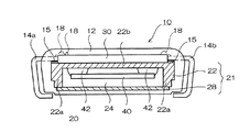
まず、本発明の圧電デバイスに係る第1の実施形態について図1、図2を参照して説明する。なお、図1は、圧電デバイスの平面を示し、図2は図1におけるA−A断面を示す図である。
本実施形態の圧電デバイス10は、圧電振動子20とこの圧電振動子20を発振制御するための回路を備えた半導体素子(IC)30とを有し、これらを樹脂12でモールドしたことを基本とする圧電発振器である。
First, a first embodiment according to the piezoelectric device of the present invention will be described with reference to FIGS. 1 is a plan view of the piezoelectric device, and FIG. 2 is a cross-sectional view taken along the line AA in FIG.
The
前記圧電振動子20は、圧電振動片40と、この圧電振動片40を収容するための振動子パッケージ(以下、単にパッケージという)21とから成る。前記圧電振動片40は、圧電材料から成る基板であり、水晶(SiO2)、ニオブ酸リチウム(LiNbO3)、タンタル酸リチウム(LiTaO3)等、種々の材料の中から選択することができるが、本実施形態においては、水晶を選択したものとして以下の説明を行う。なお、圧電振動片40はその振動特性等により、圧電基板の形状や、振動を励起するための励振電極(不図示)の形状等に違いを持つ。圧電基板の形状としては、矩形平板型のものや、音叉型の形状をしたものなどが良く知られている。前記パッケージ21は、前記圧電振動片40を収容するためのキャビティ(本実施形態では矩形状)24を有するベース22と、前記ベース22の開口部を封止するための蓋体であるリッド28とによって構成される。前記ベース22は、セラミック等の部材を箱状に焼結して形成されたものが採用されることが多く、前記リッド28は金属製、ガラス製、あるいは水晶製の平板が採用されることが多い。なお、リッド28を構成する部材の選択にあたっては、前記ベース22を構成する部材と熱膨張率が近似しているものを選択することが望ましい。また、前記ベース22内部には図示しない内部端子が設けられ、前記内部端子は、ベース22の底板22bの裏面、すなわちパッケージ21の底面に設けられた外部端子26(26a,26b,26c,26d)に電気的に接続されている。
The
本実施形態における圧電振動子20は、上記構成のベース22内に設けられた図示しない内部端子に、上記構成の圧電振動片40を導電性接着剤42等を用いて実装し、上記構成のリッド28によりベース22の開口部を気密に封止することにより構成される。
In the
前記IC30は、その回路構造、機能としては、一般的な発振器に用いられるもので良い。本実施形態で採用するIC30の基準は、そのダイサイズにある。本実施形態では、図1、及び図2に示すように、ダイサイズを定める長辺と短辺の長さのうち、少なくとも長辺の長さが、前記パッケージ21のベース22に設けられるキャビティ24の短辺長さよりも長いものを採用する。なお、本実施形態では、IC30の長辺の長さが、キャビティ24の短辺長さよりも長く、かつベース22の外形形状の短辺長さよりも短いものを選択することとする。このようなダイサイズのIC30は、一般的な圧電発振器に用いられるICよりもダイサイズの大きなものとなる。具体的には、圧電発振器に一般的に用いられるICのダイサイズを1.0mm×1.0mmとした場合、本実施形態で用いるICのダイサイズは、約1.5mm×2.0mm程度のものとなる。なお、このダイサイズの基準は参考値であり、実際の値は、パッケージ21の大きさや、実施時の技術水準等によって変化する値である。
The
上記のようなダイサイズを有するIC30は、上記構成の圧電振動子20のパッケージ21の裏面、すなわちベース22の底板22bの裏面に搭載される。パッケージ21の裏面に対するIC30の搭載に際しては、図1、及び図2に示すように、IC30の搭載面の一部が、キャビティ24を構成する側壁22aに対応した位置の底板22bの裏面に重なるようにする。なお、本実施形態では、IC30は対向する側壁22a,22a(図2参照)に対応した位置の底板22bの裏面間を跨ぐようにして配置することとする。また、IC30の搭載は、接着剤(不図示)等により、IC30の非能動面全体を接着面としてパッケージ21の裏面に接着すると良い。こうすることにより、IC30とベース22の底板22bとが一体化し、IC30はキャビティ24の天井部(図では圧電振動子を反転配置して示しているため)としての底板22bを支える梁の役割を担うこととなる。
The
本実施形態の圧電振動子20には、モールド時の支持点となる複数のリードフレーム14(14a,14b,14c,14d),16(16a,16b)が配置されている。リードフレーム14,16には、圧電デバイス10を実装するための実装電極となるリード14と、モールド時に圧電デバイス10の支持を補助するための補助リード16とがある。また、本実施形態では、パッケージ21の裏面に対して絶縁性の接着剤15を用いてリード14を接着する構成としているため、パッケージ21の裏面に設けた外部端子26と、リード14とを重ねて配置することが可能となり、圧電デバイス10全体としての小型化を促進することができるようにした。
IC30に設けられた端子32とリード14、あるいは圧電振動子20の外部端子26とは、ボンディングワイヤ18を用いたワイヤボンディングにより電気的導通が図られるように構成される。
In the
The terminal 32 and the
本実施形態の圧電デバイス10は、上記のように配置した圧電振動子20、IC30、及びリードフレーム14,16等を樹脂12によりモールドすることで体を成すが、上記構成とすることにより、樹脂モールド時の樹脂注入圧力を受けたパッケージ21が破損するということが無くなる。これは、パッケージ21の裏面に作用する樹脂注入時の圧力を、キャビティ24の側壁22a間(実際には側壁22aに対応した底板22bの裏面間)に掛け渡したIC30が緩和することにより成される作用である。すなわち、IC30の能動面に作用する樹脂注入圧力は、キャビティ24の側壁22aに分散して作用することとなるため、IC30が接着されている部分では実質的にパッケージ21の底板22bの厚みが増した効果を得ることができるのである。また、IC30の搭載面が重ならない部分の底板22bであっても、支点となる側壁22a及びIC30の接着面との境界部から圧力を受ける底板22bの中心までの距離が短くなるため、負荷圧力に対する強度が増すこととなるのである。
The
圧電振動子20に対するIC30の配置構成を上記のようなものとすることで、樹脂モールド時の樹脂注入圧力に対するパッケージ21(ベース22)の底板22bの強度を向上させることが可能となった。これにより、パッケージ21の底板22bの厚みを、さらに薄くした場合であっても樹脂注入時におけるパッケージ21の破損を防止することが可能となる。よって圧電デバイス10のさらなる薄型化を実現することが可能となる。また、採用するIC30のダイサイズを従来に比べて大きなものとすることにより、IC30の回路構成に幅を持たせることが可能となり、IC30に様々な機能を持たせることが可能となる。
By arranging the
次に、本発明の圧電デバイスに係る第2の実施形態について、図3を参照して説明する。図3に示す本実施形態の圧電デバイスの基本構成は、上述した第1の実施形態に示す圧電デバイス10と同じである。したがって、その機能を同一とする箇所には、同一の符号に100を足した符号を附して、その詳細な説明を省略することとする。
Next, a second embodiment according to the piezoelectric device of the present invention will be described with reference to FIG. The basic configuration of the piezoelectric device of this embodiment shown in FIG. 3 is the same as that of the
本実施形態に係る圧電デバイス110と、第1の実施形態に係る圧電デバイス10との相違点は、デバイスの実装用電極としての機能を担うリード114(114a,114b,114c,114d)や、補助リード116(116a,116b)等のリードフレームを、圧電振動子120に取り付けるにあたり、その取り付け位置を、前記パッケージ121の側壁122aに対応した位置を越える範囲、すなわち、側壁122aとその内側の領域に亙る底板(図2で示す22b)の裏面に取り付けたことである。このような配置構成で、リード114や補助リード116を取り付けることにより、第1の実施形態で述べたIC30の配置構成の効果と同様、キャビティ124の天井としての底板をリードフレーム114,116によって吊った状態を構成することとなり、パッケージ21の底板が補強されることとなる。このため、樹脂モールド時の樹脂注入圧力に対するパッケージ121の底板の強度を、さらに向上させることが可能となる。なお、他の構成、及び作用効果は、上記第1の実施形態に示した圧電デバイス10と同様である。
The difference between the
次に、本発明の圧電デバイスに係る第3の実施形態について、図4を参照して説明する。なお、本実施形態以下の実施形態では、説明を簡単化するために、圧電振動子の裏面に対する電子部品の配置形態のみを特徴的に図面に示し、リードフレーム、ボンディングワイヤ等、その他の構成は第1の実施形態、第2の実施形態、及び本願出願時にすでに知られている一般の圧電デバイスの例に倣うこととする。なお図4において、上記第1の実施形態に示す圧電デバイスとその機能を同一とする部分には、図1に示す符号に200を足した符号を附して、その詳細な説明は省略することとする。 Next, a third embodiment according to the piezoelectric device of the present invention will be described with reference to FIG. In the following embodiments, in order to simplify the description, only the arrangement form of the electronic components with respect to the back surface of the piezoelectric vibrator is characteristically shown in the drawings, and other configurations such as a lead frame and bonding wires are not shown. The example of the first embodiment, the second embodiment, and a general piezoelectric device already known at the time of filing of the present application will be followed. In FIG. 4, parts having the same functions as those of the piezoelectric device shown in the first embodiment are denoted by reference numerals obtained by adding 200 to the reference numerals shown in FIG. And
図4において、パッケージ221の裏面中央に示す2点鎖線で囲う領域は、本実施形態に採用するIC230のダイサイズを示すものである。なお、本実施形態の圧電デバイスに採用するIC230のダイサイズは、一般的な圧電発振器に用いられるICのダイサイズと同じで良い。上述した例に倣えばIC230のダイサイズは1mm角である。このダイサイズのIC230は、図4からも読みとれるように、パッケージ221の裏面中央に配置したのでは、側壁に対応した位置の底板(図2で示す22b)の裏面に接着面を重ねることはできない。このため、IC230の配置形態を従来通りパッケージ221裏面の中央に設定した場合には、樹脂モールド時に生じる樹脂注入圧力により、パッケージ221の底板に破損が生じる可能性がある。
In FIG. 4, a region surrounded by a two-dot chain line at the center of the back surface of the
そこで本実施形態では、パッケージ221の裏面に対するIC230の配置位置を、キャビティ224を構成するいずれかの側壁222aに対応した底板の裏面にまでシフトさせ、いずれか1つの辺のみを側壁222aに対応した位置の底板の裏面に配置するようにした。パッケージ221の裏面に対するIC230の配置構成を、上記のようなものとした場合であっても、樹脂モールド時にパッケージ221の底板に負荷される樹脂注入圧力を緩和することができる。よって、上記第1、第2の実施形態と同様に、パッケージ221の底板を薄くした場合であっても、樹脂注入圧力を受けたパッケージ221の底板が破損するということがなくなり、圧電デバイスの薄型化を実現することが可能となる。また、本実施形態のようなIC230の配置形態であれば、圧電デバイスを構成する部品自体は従来の構成の圧電デバイスと変わらないものを採用することができるため、大幅な設計変更等が不要となる。
Therefore, in the present embodiment, the arrangement position of the
次に、本発明の圧電デバイスに係る第4の実施形態について、図5を参照して説明する。なお、本実施形態に示す圧電デバイスは、上記第3の実施形態に示した圧電デバイスとの対比において、電子部品であるICの配置形態を異ならせたことのみを特徴とするものである。したがって、その機能を同一とする箇所には、図面に図4に示す符号と同一の符号を附して詳細な説明は省略することとする。 Next, a fourth embodiment according to the piezoelectric device of the present invention will be described with reference to FIG. Note that the piezoelectric device shown in the present embodiment is characterized only in that the arrangement form of ICs as electronic components is different in comparison with the piezoelectric device shown in the third embodiment. Therefore, portions having the same functions are denoted by the same reference numerals as those shown in FIG. 4 in the drawing, and detailed description thereof will be omitted.
本実施形態の圧電デバイスは、IC230の配置位置を、パッケージ221の角部、すなわちキャビティ224を構成する側壁222aが交わる位置へシフトさせたことを特徴とする。IC230をこのような配置形態で配置することにより、パッケージ221における長辺側の側壁222a1と短辺側の側壁222a2とのそれぞれに対応した位置の底板(図2で示す22b)の裏面にIC230を配置することが可能となり、安定した接着状態を保つことが可能となる。また、直交する2つの側壁222a1,222a2にてIC230を支持することとなるため、IC230の能動面に作用する樹脂注入圧力は、前記側壁222a1,222a2側へ分散されることとなり、パッケージ221の底板に負荷される圧力を緩和することができるようになる。このように、本実施形態のIC230は、2つの側壁222a1,222a2で支持されることとなるため、1つの側壁での支持となる第3の実施形態に係る圧電デバイスよりも、パッケージ221の底板の耐圧性を高めることができる。
The piezoelectric device according to the present embodiment is characterized in that the arrangement position of the
次に、本発明の圧電デバイスに係る第5の実施形態について、図6を参照して説明する。なお、本実施形態に示す圧電デバイスは、上記第3の実施形態に示した圧電デバイスとの対比において、電子部品であるICの配置形態を異ならせたことのみを特徴とするものである。したがって、その機能を同一とする箇所には、図面に図4と同一の符号を附して詳細な説明は省略することとする。 Next, a fifth embodiment of the piezoelectric device of the present invention will be described with reference to FIG. Note that the piezoelectric device shown in the present embodiment is characterized only in that the arrangement form of ICs as electronic components is different in comparison with the piezoelectric device shown in the third embodiment. Therefore, portions having the same function are denoted by the same reference numerals as those in FIG. 4 and detailed description thereof is omitted.
本実施形態の圧電デバイスは、IC230の配置形態を、回転シフトさせたことを特徴とする。このようにIC230の配置形態に回転を加え、パッケージ221の辺に対してIC230の辺を傾けて配置することにより、小さなIC(ICは矩形状であると仮定する)であっても、パッケージ221においてキャビティ224を構成する対向した側壁222a,222aに対応した位置の底板(図2で示す22b)の裏面間を跨いで設置面の対角を配置することができる。こうすることでIC230の能動面に付加される樹脂の注入圧力は、パッケージ221の側壁222a,222aへと分散されることとなるため、パッケージ221の底板に負荷される圧力を緩和することができ、上述した第1、第2の実施形態と同様の作用効果を得ることができることとなる。
The piezoelectric device of this embodiment is characterized in that the arrangement form of the
次に、本発明の圧電デバイスに係る第6の実施形態について、図7を参照して説明する。なお、本実施形態に示す圧電デバイスは、上記第3乃至第5の実施形態に示した圧電デバイスがICの配置形態に変化を加えたことを特徴にしていることに対して、ICのダイサイズ自体を変えたことを特徴とするものであり、実質的作用効果は、上記第1、第2の実施形態と同様である。したがって、その機能を同一とする箇所には、図面に図4と同一の符号を附して詳細な説明は省略することとする。 Next, a sixth embodiment according to the piezoelectric device of the present invention will be described with reference to FIG. Note that the piezoelectric device shown in the present embodiment is characterized in that the piezoelectric device shown in the third to fifth embodiments is changed in the IC arrangement, whereas the die size of the IC. It is characterized by changing itself, and the substantial operational effect is the same as in the first and second embodiments. Therefore, portions having the same function are denoted by the same reference numerals as those in FIG. 4 and detailed description thereof is omitted.
本実施形態の圧電デバイスでは、IC230aのダイサイズを、2点鎖線で示す一般的なIC230のダイサイズに比べて大きなものとしたことを特徴とする。ICのダイサイズを大きくすることにより、IC230aを、パッケージ221においてキャビティ224を構成する対向した側壁222a,222aに対応した位置の底板(図2で示す22b)の裏面間に亙って配置することが可能となる。これにより、上記第1、第2の実施形態に示した圧電デバイスと同様の効果を得ることができる。
The piezoelectric device of the present embodiment is characterized in that the die size of the
上記それぞれの実施形態では、電子部品としてICのみを挙げ、そのICの配置形態のみに特徴を持たせてきた。しかし、本発明に係る圧電デバイスでは、温度補償型圧電発振器等の圧電デバイスに搭載されるサーミスタ等のIC以外の電子部品を搭載する場合にも適用することができる。図8にこの場合の例を示し、以下に電子部品と圧電振動子との関係を説明する。なお、上述した各実施形態に係る圧電デバイスと、その機能を同一とする箇所には、図面に図1の符号に300を足した符号を附して詳細な説明を省略することとする。 In each of the above embodiments, only the IC is cited as the electronic component, and only the arrangement form of the IC has been characterized. However, the piezoelectric device according to the present invention can also be applied to the case where electronic components other than an IC such as a thermistor mounted on a piezoelectric device such as a temperature compensated piezoelectric oscillator are mounted. FIG. 8 shows an example of this case, and the relationship between the electronic component and the piezoelectric vibrator will be described below. In addition, the piezoelectric device which concerns on each embodiment mentioned above, and the location which makes the function the same attach | subject the code | symbol which added 300 to the code | symbol of FIG. 1, and abbreviate | omits detailed description.
本実施形態の圧電デバイスも、上記種々の実施形態に示した圧電デバイスと同様、IC330をパッケージ321における側壁322aに対応した底板(図2で示す22b)の裏面に配置する。また、サーミスタ等のIC以外の電子部品334a,334bも同様に、側壁322aに対応した底板の裏面に配置することが望ましい。このように、圧電デバイスを構成し、圧電振動子320の周囲に配置する電子部品を、パッケージ321の側壁322aに対応した底板の裏面上、すなわちキャビティ324の天井である底板と、側壁322aとを跨ぐ位置の底板裏面に配置することで、パッケージ321の底板の強度を補強する効果を奏することができ、底板を薄くした場合であっても高い樹脂注入圧力に耐えることが可能となる。よって、圧電デバイスの薄型化を実現することが可能となる。なお、IC330や他の電子部品334a,334bが大型のものである場合には、上記実施形態に示したように、キャビティ324を構成する対向した側壁322a,322aに対応した位置の底板の裏面間を跨ぐように配置すると良い。
Also in the piezoelectric device of this embodiment, the
なお、上記第3の実施形態以下の実施形態では、リードフレームやボンディングワイヤの構成を図面に明記していないが、これらの配置、接続形態は、図1乃至図3、及び既知の技術より構成し得るものである。 In the third embodiment and the following embodiments, the configuration of the lead frame and the bonding wire is not clearly shown in the drawings. However, the arrangement and connection form thereof are configured from FIGS. 1 to 3 and a known technique. It is possible.
次に、上述した各圧電デバイス(圧電発振器)を搭載する電子機器の一実施形態として携帯電話装置の構成について図9を参照して説明する。
携帯電話装置400では、送信者からの音声信号は、マイクロフォン402によって電気信号に変換され、デモジュレータ・コーデック等を備える信号切替部406で変調等され、送信部408にて周波数変換等され、アンテナ412を介して基地局(不図示)に送信される。
Next, a configuration of a mobile phone device will be described with reference to FIG. 9 as an embodiment of an electronic apparatus in which each piezoelectric device (piezoelectric oscillator) described above is mounted.
In the cellular phone device 400, the audio signal from the transmitter is converted into an electric signal by the
これに対し、基地局から送信された信号は、アンテナ412を介して受信し、受信部414にて周波数変換され、信号切替部406にて音声信号に変換されて、スピーカ404から出力される。
On the other hand, the signal transmitted from the base station is received via the
このような信号制御が成される携帯電話装置400の動作は、CPU(Central Processing Unit)416によって全体が制御されている。CPU416は、液晶画面やキーボード等の入出力部418や、制御プログラムや電話帳等を記録するメモリ420をはじめ、信号の送受信を制御する切替スイッチ410の動作も制御している。
The operation of the mobile phone device 400 in which such signal control is performed is entirely controlled by a CPU (Central Processing Unit) 416. The
上記のような基本構成を有する携帯電話装置において、上述した圧電デバイスは特に、CPU416に接続され、CPU416の基本クロック等の役割を果たす。このようにして、上記のような構成の圧電デバイスを搭載することにより、携帯電話装置の小型化、薄型化、あるいは高集積化を実現することが可能となる。
In the mobile phone device having the basic configuration as described above, the above-described piezoelectric device is connected to the
10………圧電デバイス、12………樹脂、14(14a〜14d)………リード(リードフレーム)、16(16a,16b)………補助リード(リードフレーム)、18………ボンディングワイヤ、20………圧電振動子、21………パッケージ(振動子パッケージ)、22………ベース、22a………側壁、22b………底板、24………キャビティ、26(26a〜26d)………外部端子、28………リッド、30………IC、32………端子、40………圧電振動片、42………導電性接着剤。
10 ......... Piezoelectric device, 12 ......... Resin, 14 (14a to 14d) ......... Lead (lead frame), 16 (16a, 16b) ......... Auxiliary lead (lead frame), 18 .........
Claims (7)
前記電子部品は、前記振動子パッケージにおける前記圧電振動片を収容するキャビティを構成する側壁に対応した位置の裏面に、少なくとも設置面の一部を重ねて配置したことを特徴とする圧電デバイス。 A piezoelectric device having a vibrator package containing a piezoelectric vibrating piece therein and an electronic component fixed to the back surface of the vibrator package, wherein the vibrator package and the electronic component are molded with a resin,
The piezoelectric device according to claim 1, wherein the electronic component is arranged such that at least a part of an installation surface is overlapped with a back surface at a position corresponding to a side wall constituting a cavity for housing the piezoelectric vibrating piece in the vibrator package.
前記電子部品は、前記振動子パッケージにおける前記圧電振動片を収容するキャビティを構成する対向した側壁に対応した位置の裏面間を跨ぐ大きさのダイサイズを有するものを採用し、前記裏面間を跨いで配置することを特徴とする圧電デバイス。 A piezoelectric device having a vibrator package containing a piezoelectric vibrating piece therein and an electronic component fixed to the back surface of the vibrator package, wherein the vibrator package and the electronic component are molded with a resin,
The electronic component employs an electronic component having a die size that spans between the back surfaces at positions corresponding to opposing side walls that constitute the cavity that accommodates the piezoelectric vibrating piece in the vibrator package, and straddles between the back surfaces. A piezoelectric device characterized by being arranged by
前記リードフレームは、前記振動子パッケージにおける前記キャビティと前記側壁とのそれぞれに対応した位置の裏面を跨いで配置したことを特徴とする請求項1乃至請求項3のいずれかに記載の圧電デバイス。 A lead frame that penetrates the resin mold part is attached to the piezoelectric vibrator,
4. The piezoelectric device according to claim 1, wherein the lead frame is disposed across a back surface at a position corresponding to each of the cavity and the side wall of the vibrator package. 5.
Priority Applications (1)
| Application Number | Priority Date | Filing Date | Title |
|---|---|---|---|
| JP2006004482A JP2007189380A (en) | 2006-01-12 | 2006-01-12 | Piezoelectric device and electronic equipment |
Applications Claiming Priority (1)
| Application Number | Priority Date | Filing Date | Title |
|---|---|---|---|
| JP2006004482A JP2007189380A (en) | 2006-01-12 | 2006-01-12 | Piezoelectric device and electronic equipment |
Publications (2)
| Publication Number | Publication Date |
|---|---|
| JP2007189380A true JP2007189380A (en) | 2007-07-26 |
| JP2007189380A5 JP2007189380A5 (en) | 2009-02-05 |
Family
ID=38344262
Family Applications (1)
| Application Number | Title | Priority Date | Filing Date |
|---|---|---|---|
| JP2006004482A Withdrawn JP2007189380A (en) | 2006-01-12 | 2006-01-12 | Piezoelectric device and electronic equipment |
Country Status (1)
| Country | Link |
|---|---|
| JP (1) | JP2007189380A (en) |
Cited By (1)
| Publication number | Priority date | Publication date | Assignee | Title |
|---|---|---|---|---|
| JP7353156B2 (en) | 2019-11-29 | 2023-09-29 | 日本電波工業株式会社 | oscillator |
Citations (6)
| Publication number | Priority date | Publication date | Assignee | Title |
|---|---|---|---|---|
| JPS6253811A (en) * | 1985-09-03 | 1987-03-09 | Inoue Mtp Co Ltd | Manufacture of laminated material |
| JP2004297770A (en) * | 2003-03-13 | 2004-10-21 | Seiko Epson Corp | Piezoelectric vibrator device, portable telephone set and electronic equipment using it |
| JP2005033761A (en) * | 2003-06-16 | 2005-02-03 | Seiko Epson Corp | Piezoelectric oscillator, manufacturing method therefor, mobile phone apparatus using piezoelectric oscillator, and electronic apparatus using piezoelectric oscillator |
| JP2005244922A (en) * | 2004-01-29 | 2005-09-08 | Kyocera Corp | Piezoelectric oscillator |
| JP2005244501A (en) * | 2004-02-25 | 2005-09-08 | Seiko Epson Corp | Piezoelectric oscillator |
| JP2005318524A (en) * | 2004-04-01 | 2005-11-10 | Seiko Epson Corp | Piezoelectric oscillator and method of manufacturing the same |
-
2006
- 2006-01-12 JP JP2006004482A patent/JP2007189380A/en not_active Withdrawn
Patent Citations (6)
| Publication number | Priority date | Publication date | Assignee | Title |
|---|---|---|---|---|
| JPS6253811A (en) * | 1985-09-03 | 1987-03-09 | Inoue Mtp Co Ltd | Manufacture of laminated material |
| JP2004297770A (en) * | 2003-03-13 | 2004-10-21 | Seiko Epson Corp | Piezoelectric vibrator device, portable telephone set and electronic equipment using it |
| JP2005033761A (en) * | 2003-06-16 | 2005-02-03 | Seiko Epson Corp | Piezoelectric oscillator, manufacturing method therefor, mobile phone apparatus using piezoelectric oscillator, and electronic apparatus using piezoelectric oscillator |
| JP2005244922A (en) * | 2004-01-29 | 2005-09-08 | Kyocera Corp | Piezoelectric oscillator |
| JP2005244501A (en) * | 2004-02-25 | 2005-09-08 | Seiko Epson Corp | Piezoelectric oscillator |
| JP2005318524A (en) * | 2004-04-01 | 2005-11-10 | Seiko Epson Corp | Piezoelectric oscillator and method of manufacturing the same |
Cited By (1)
| Publication number | Priority date | Publication date | Assignee | Title |
|---|---|---|---|---|
| JP7353156B2 (en) | 2019-11-29 | 2023-09-29 | 日本電波工業株式会社 | oscillator |
Similar Documents
| Publication | Publication Date | Title |
|---|---|---|
| JP4314999B2 (en) | Piezoelectric oscillator, mobile phone device using piezoelectric oscillator, and electronic device using piezoelectric oscillator | |
| JP2009213061A (en) | Oscillator and electronic device | |
| US20100045393A1 (en) | Crystal oscillator | |
| JP2010050778A (en) | Piezoelectric device | |
| JP2004208237A (en) | Piezoelectric device, mobile telephone equipment utilizing piezoelectric device, and electronic equipment utilizing piezoelectric device | |
| JP2000278079A (en) | Piezoelectric device | |
| JP2007189282A (en) | Piezoelectric device and manufacturing method thereof | |
| JP2007189380A (en) | Piezoelectric device and electronic equipment | |
| JP2007096529A (en) | Piezoelectric vibration element, supporting structure of piezoelectric vibration element, surface mounting type piezoelectric vibrator, and surface mounting type piezoelectric oscillator | |
| JP2007324933A (en) | Piezoelectric oscillator and its manufacturing method | |
| JP2007318286A (en) | Piezoelectric device | |
| JP2007235791A (en) | Piezoelectric device | |
| JP2005012635A (en) | Piezoelectric device | |
| JP4721101B2 (en) | Piezoelectric device, method for manufacturing piezoelectric device, and electronic apparatus | |
| JP2011055083A (en) | Method of manufacturing piezoelectric device, and piezoelectric device | |
| JP4587727B2 (en) | Piezoelectric vibrator storage package and piezoelectric device | |
| JP2007300173A (en) | Package for electronic device, and electronic device | |
| JP4587730B2 (en) | Piezoelectric vibrator storage package and piezoelectric device | |
| JP3620451B2 (en) | Package structure of piezoelectric device | |
| JP2006060280A (en) | Manufacturing method for piezoelectric oscillator and piezoelectric oscillator | |
| KR20070016318A (en) | Multi mode crystal oscillator | |
| JP2003060474A (en) | Piezoelectric device, and mobile telephone apparatus and electronic appliance utilizing the piezoelectric device | |
| JP2006325052A5 (en) | ||
| JP2004274657A (en) | Package sealing hole shape setting method, piezo-electric device package, and piezo-electric device | |
| JP2007013721A (en) | Piezoelectric oscillator |
Legal Events
| Date | Code | Title | Description |
|---|---|---|---|
| A521 | Written amendment |
Free format text: JAPANESE INTERMEDIATE CODE: A523 Effective date: 20081212 |
|
| A621 | Written request for application examination |
Effective date: 20081212 Free format text: JAPANESE INTERMEDIATE CODE: A621 |
|
| A711 | Notification of change in applicant |
Effective date: 20110729 Free format text: JAPANESE INTERMEDIATE CODE: A712 |
|
| RD03 | Notification of appointment of power of attorney |
Effective date: 20110729 Free format text: JAPANESE INTERMEDIATE CODE: A7423 |
|
| A977 | Report on retrieval |
Free format text: JAPANESE INTERMEDIATE CODE: A971007 Effective date: 20110817 |
|
| A521 | Written amendment |
Free format text: JAPANESE INTERMEDIATE CODE: A523 Effective date: 20110819 |
|
| A131 | Notification of reasons for refusal |
Effective date: 20110927 Free format text: JAPANESE INTERMEDIATE CODE: A131 |
|
| A521 | Written amendment |
Free format text: JAPANESE INTERMEDIATE CODE: A523 Effective date: 20111118 |
|
| A131 | Notification of reasons for refusal |
Free format text: JAPANESE INTERMEDIATE CODE: A131 Effective date: 20120207 |
|
| A761 | Written withdrawal of application |
Effective date: 20120224 Free format text: JAPANESE INTERMEDIATE CODE: A761 |