EP1458086B1 - Piezoelectric Oscillator - Google Patents
Piezoelectric Oscillator Download PDFInfo
- Publication number
- EP1458086B1 EP1458086B1 EP04005790A EP04005790A EP1458086B1 EP 1458086 B1 EP1458086 B1 EP 1458086B1 EP 04005790 A EP04005790 A EP 04005790A EP 04005790 A EP04005790 A EP 04005790A EP 1458086 B1 EP1458086 B1 EP 1458086B1
- Authority
- EP
- European Patent Office
- Prior art keywords
- resonator package
- inner lead
- rear surface
- terminals
- piezoelectric
- Prior art date
- Legal status (The legal status is an assumption and is not a legal conclusion. Google has not performed a legal analysis and makes no representation as to the accuracy of the status listed.)
- Expired - Lifetime
Links
- 239000004065 semiconductor Substances 0.000 claims description 22
- 229920005989 resin Polymers 0.000 claims description 15
- 239000011347 resin Substances 0.000 claims description 15
- 229910052751 metal Inorganic materials 0.000 claims description 3
- 239000002184 metal Substances 0.000 claims description 3
- 239000000853 adhesive Substances 0.000 description 15
- 230000001070 adhesive effect Effects 0.000 description 15
- 238000010276 construction Methods 0.000 description 6
- 238000004519 manufacturing process Methods 0.000 description 6
- 239000010453 quartz Substances 0.000 description 6
- VYPSYNLAJGMNEJ-UHFFFAOYSA-N silicon dioxide Inorganic materials O=[Si]=O VYPSYNLAJGMNEJ-UHFFFAOYSA-N 0.000 description 6
- 238000000034 method Methods 0.000 description 5
- 230000008878 coupling Effects 0.000 description 3
- 238000010168 coupling process Methods 0.000 description 3
- 238000005859 coupling reaction Methods 0.000 description 3
- 230000000694 effects Effects 0.000 description 3
- PCHJSUWPFVWCPO-UHFFFAOYSA-N gold Chemical compound [Au] PCHJSUWPFVWCPO-UHFFFAOYSA-N 0.000 description 3
- 239000000463 material Substances 0.000 description 3
- 229920003002 synthetic resin Polymers 0.000 description 3
- 239000000057 synthetic resin Substances 0.000 description 3
- 239000004593 Epoxy Substances 0.000 description 2
- PXHVJJICTQNCMI-UHFFFAOYSA-N Nickel Chemical compound [Ni] PXHVJJICTQNCMI-UHFFFAOYSA-N 0.000 description 2
- 239000000919 ceramic Substances 0.000 description 2
- 238000010292 electrical insulation Methods 0.000 description 2
- 230000005284 excitation Effects 0.000 description 2
- 238000007689 inspection Methods 0.000 description 2
- 238000009413 insulation Methods 0.000 description 2
- 238000000465 moulding Methods 0.000 description 2
- 239000002245 particle Substances 0.000 description 2
- 238000007747 plating Methods 0.000 description 2
- 238000007789 sealing Methods 0.000 description 2
- 229910000679 solder Inorganic materials 0.000 description 2
- 239000000758 substrate Substances 0.000 description 2
- WSMQKESQZFQMFW-UHFFFAOYSA-N 5-methyl-pyrazole-3-carboxylic acid Chemical compound CC1=CC(C(O)=O)=NN1 WSMQKESQZFQMFW-UHFFFAOYSA-N 0.000 description 1
- 229910017518 Cu Zn Inorganic materials 0.000 description 1
- 229910000881 Cu alloy Inorganic materials 0.000 description 1
- 229910017755 Cu-Sn Inorganic materials 0.000 description 1
- 229910017752 Cu-Zn Inorganic materials 0.000 description 1
- 229910002482 Cu–Ni Inorganic materials 0.000 description 1
- 229910017827 Cu—Fe Inorganic materials 0.000 description 1
- 229910017927 Cu—Sn Inorganic materials 0.000 description 1
- 229910017943 Cu—Zn Inorganic materials 0.000 description 1
- 229910000640 Fe alloy Inorganic materials 0.000 description 1
- 101000710013 Homo sapiens Reversion-inducing cysteine-rich protein with Kazal motifs Proteins 0.000 description 1
- 101000661807 Homo sapiens Suppressor of tumorigenicity 14 protein Proteins 0.000 description 1
- 229910017709 Ni Co Inorganic materials 0.000 description 1
- 229910003267 Ni-Co Inorganic materials 0.000 description 1
- 229910003262 Ni‐Co Inorganic materials 0.000 description 1
- 239000004642 Polyimide Substances 0.000 description 1
- XUIMIQQOPSSXEZ-UHFFFAOYSA-N Silicon Chemical compound [Si] XUIMIQQOPSSXEZ-UHFFFAOYSA-N 0.000 description 1
- 229910045601 alloy Inorganic materials 0.000 description 1
- 239000000956 alloy Substances 0.000 description 1
- 238000005452 bending Methods 0.000 description 1
- 230000008901 benefit Effects 0.000 description 1
- 230000015556 catabolic process Effects 0.000 description 1
- 230000008859 change Effects 0.000 description 1
- 239000003795 chemical substances by application Substances 0.000 description 1
- 239000011248 coating agent Substances 0.000 description 1
- 238000000576 coating method Methods 0.000 description 1
- KUNSUQLRTQLHQQ-UHFFFAOYSA-N copper tin Chemical compound [Cu].[Sn] KUNSUQLRTQLHQQ-UHFFFAOYSA-N 0.000 description 1
- TVZPLCNGKSPOJA-UHFFFAOYSA-N copper zinc Chemical compound [Cu].[Zn] TVZPLCNGKSPOJA-UHFFFAOYSA-N 0.000 description 1
- 239000013078 crystal Substances 0.000 description 1
- 238000005520 cutting process Methods 0.000 description 1
- 238000006731 degradation reaction Methods 0.000 description 1
- 230000001419 dependent effect Effects 0.000 description 1
- 239000003822 epoxy resin Substances 0.000 description 1
- 239000010946 fine silver Substances 0.000 description 1
- 239000011521 glass Substances 0.000 description 1
- 229910052737 gold Inorganic materials 0.000 description 1
- 239000010931 gold Substances 0.000 description 1
- 230000017525 heat dissipation Effects 0.000 description 1
- 239000011810 insulating material Substances 0.000 description 1
- 108090000237 interleukin-24 Proteins 0.000 description 1
- 238000010030 laminating Methods 0.000 description 1
- 239000004973 liquid crystal related substance Substances 0.000 description 1
- GQYHUHYESMUTHG-UHFFFAOYSA-N lithium niobate Chemical compound [Li+].[O-][Nb](=O)=O GQYHUHYESMUTHG-UHFFFAOYSA-N 0.000 description 1
- 229910001092 metal group alloy Inorganic materials 0.000 description 1
- 238000010295 mobile communication Methods 0.000 description 1
- 229910052759 nickel Inorganic materials 0.000 description 1
- TWNQGVIAIRXVLR-UHFFFAOYSA-N oxo(oxoalumanyloxy)alumane Chemical compound O=[Al]O[Al]=O TWNQGVIAIRXVLR-UHFFFAOYSA-N 0.000 description 1
- 229920000647 polyepoxide Polymers 0.000 description 1
- 229920001721 polyimide Polymers 0.000 description 1
- 229920001296 polysiloxane Polymers 0.000 description 1
- 230000008569 process Effects 0.000 description 1
- 230000004044 response Effects 0.000 description 1
- 238000007493 shaping process Methods 0.000 description 1
- 229910052710 silicon Inorganic materials 0.000 description 1
- 239000010703 silicon Substances 0.000 description 1
- 238000005245 sintering Methods 0.000 description 1
- 230000005236 sound signal Effects 0.000 description 1
- 125000006850 spacer group Chemical group 0.000 description 1
- 238000003860 storage Methods 0.000 description 1
- 229910002058 ternary alloy Inorganic materials 0.000 description 1
- WFKWXMTUELFFGS-UHFFFAOYSA-N tungsten Chemical compound [W] WFKWXMTUELFFGS-UHFFFAOYSA-N 0.000 description 1
- 229910052721 tungsten Inorganic materials 0.000 description 1
- 239000010937 tungsten Substances 0.000 description 1
Images


Classifications
-
- H—ELECTRICITY
- H03—ELECTRONIC CIRCUITRY
- H03B—GENERATION OF OSCILLATIONS, DIRECTLY OR BY FREQUENCY-CHANGING, BY CIRCUITS EMPLOYING ACTIVE ELEMENTS WHICH OPERATE IN A NON-SWITCHING MANNER; GENERATION OF NOISE BY SUCH CIRCUITS
- H03B5/00—Generation of oscillations using amplifier with regenerative feedback from output to input
- H03B5/30—Generation of oscillations using amplifier with regenerative feedback from output to input with frequency-determining element being electromechanical resonator
- H03B5/32—Generation of oscillations using amplifier with regenerative feedback from output to input with frequency-determining element being electromechanical resonator being a piezoelectric resonator
- H03B5/36—Generation of oscillations using amplifier with regenerative feedback from output to input with frequency-determining element being electromechanical resonator being a piezoelectric resonator active element in amplifier being semiconductor device
-
- F—MECHANICAL ENGINEERING; LIGHTING; HEATING; WEAPONS; BLASTING
- F16—ENGINEERING ELEMENTS AND UNITS; GENERAL MEASURES FOR PRODUCING AND MAINTAINING EFFECTIVE FUNCTIONING OF MACHINES OR INSTALLATIONS; THERMAL INSULATION IN GENERAL
- F16H—GEARING
- F16H63/00—Control outputs from the control unit to change-speed- or reversing-gearings for conveying rotary motion or to other devices than the final output mechanism
- F16H63/02—Final output mechanisms therefor; Actuating means for the final output mechanisms
- F16H63/30—Constructional features of the final output mechanisms
-
- F—MECHANICAL ENGINEERING; LIGHTING; HEATING; WEAPONS; BLASTING
- F16—ENGINEERING ELEMENTS AND UNITS; GENERAL MEASURES FOR PRODUCING AND MAINTAINING EFFECTIVE FUNCTIONING OF MACHINES OR INSTALLATIONS; THERMAL INSULATION IN GENERAL
- F16H—GEARING
- F16H57/00—General details of gearing
- F16H57/02—Gearboxes; Mounting gearing therein
- F16H2057/02039—Gearboxes for particular applications
- F16H2057/02043—Gearboxes for particular applications for vehicle transmissions
- F16H2057/02052—Axle units; Transfer casings for four wheel drive
-
- F—MECHANICAL ENGINEERING; LIGHTING; HEATING; WEAPONS; BLASTING
- F16—ENGINEERING ELEMENTS AND UNITS; GENERAL MEASURES FOR PRODUCING AND MAINTAINING EFFECTIVE FUNCTIONING OF MACHINES OR INSTALLATIONS; THERMAL INSULATION IN GENERAL
- F16H—GEARING
- F16H63/00—Control outputs from the control unit to change-speed- or reversing-gearings for conveying rotary motion or to other devices than the final output mechanism
- F16H63/02—Final output mechanisms therefor; Actuating means for the final output mechanisms
- F16H63/30—Constructional features of the final output mechanisms
- F16H2063/3079—Shift rod assembly, e.g. supporting, assembly or manufacturing of shift rails or rods; Special details thereof
-
- F—MECHANICAL ENGINEERING; LIGHTING; HEATING; WEAPONS; BLASTING
- F16—ENGINEERING ELEMENTS AND UNITS; GENERAL MEASURES FOR PRODUCING AND MAINTAINING EFFECTIVE FUNCTIONING OF MACHINES OR INSTALLATIONS; THERMAL INSULATION IN GENERAL
- F16H—GEARING
- F16H63/00—Control outputs from the control unit to change-speed- or reversing-gearings for conveying rotary motion or to other devices than the final output mechanism
- F16H63/02—Final output mechanisms therefor; Actuating means for the final output mechanisms
- F16H63/30—Constructional features of the final output mechanisms
- F16H63/32—Gear shift yokes, e.g. shift forks
- F16H2063/321—Gear shift yokes, e.g. shift forks characterised by the interface between fork body and shift rod, e.g. fixing means, bushes, cams or pins
-
- H—ELECTRICITY
- H01—ELECTRIC ELEMENTS
- H01L—SEMICONDUCTOR DEVICES NOT COVERED BY CLASS H10
- H01L2224/00—Indexing scheme for arrangements for connecting or disconnecting semiconductor or solid-state bodies and methods related thereto as covered by H01L24/00
- H01L2224/01—Means for bonding being attached to, or being formed on, the surface to be connected, e.g. chip-to-package, die-attach, "first-level" interconnects; Manufacturing methods related thereto
- H01L2224/02—Bonding areas; Manufacturing methods related thereto
- H01L2224/04—Structure, shape, material or disposition of the bonding areas prior to the connecting process
- H01L2224/05—Structure, shape, material or disposition of the bonding areas prior to the connecting process of an individual bonding area
- H01L2224/0554—External layer
- H01L2224/0555—Shape
- H01L2224/05552—Shape in top view
- H01L2224/05554—Shape in top view being square
-
- H—ELECTRICITY
- H01—ELECTRIC ELEMENTS
- H01L—SEMICONDUCTOR DEVICES NOT COVERED BY CLASS H10
- H01L2224/00—Indexing scheme for arrangements for connecting or disconnecting semiconductor or solid-state bodies and methods related thereto as covered by H01L24/00
- H01L2224/01—Means for bonding being attached to, or being formed on, the surface to be connected, e.g. chip-to-package, die-attach, "first-level" interconnects; Manufacturing methods related thereto
- H01L2224/42—Wire connectors; Manufacturing methods related thereto
- H01L2224/44—Structure, shape, material or disposition of the wire connectors prior to the connecting process
- H01L2224/45—Structure, shape, material or disposition of the wire connectors prior to the connecting process of an individual wire connector
- H01L2224/45001—Core members of the connector
- H01L2224/45099—Material
- H01L2224/451—Material with a principal constituent of the material being a metal or a metalloid, e.g. boron (B), silicon (Si), germanium (Ge), arsenic (As), antimony (Sb), tellurium (Te) and polonium (Po), and alloys thereof
- H01L2224/45138—Material with a principal constituent of the material being a metal or a metalloid, e.g. boron (B), silicon (Si), germanium (Ge), arsenic (As), antimony (Sb), tellurium (Te) and polonium (Po), and alloys thereof the principal constituent melting at a temperature of greater than or equal to 950°C and less than 1550°C
- H01L2224/45144—Gold (Au) as principal constituent
-
- H—ELECTRICITY
- H01—ELECTRIC ELEMENTS
- H01L—SEMICONDUCTOR DEVICES NOT COVERED BY CLASS H10
- H01L2224/00—Indexing scheme for arrangements for connecting or disconnecting semiconductor or solid-state bodies and methods related thereto as covered by H01L24/00
- H01L2224/01—Means for bonding being attached to, or being formed on, the surface to be connected, e.g. chip-to-package, die-attach, "first-level" interconnects; Manufacturing methods related thereto
- H01L2224/42—Wire connectors; Manufacturing methods related thereto
- H01L2224/47—Structure, shape, material or disposition of the wire connectors after the connecting process
- H01L2224/48—Structure, shape, material or disposition of the wire connectors after the connecting process of an individual wire connector
- H01L2224/4805—Shape
- H01L2224/4809—Loop shape
- H01L2224/48091—Arched
-
- H—ELECTRICITY
- H01—ELECTRIC ELEMENTS
- H01L—SEMICONDUCTOR DEVICES NOT COVERED BY CLASS H10
- H01L2224/00—Indexing scheme for arrangements for connecting or disconnecting semiconductor or solid-state bodies and methods related thereto as covered by H01L24/00
- H01L2224/01—Means for bonding being attached to, or being formed on, the surface to be connected, e.g. chip-to-package, die-attach, "first-level" interconnects; Manufacturing methods related thereto
- H01L2224/42—Wire connectors; Manufacturing methods related thereto
- H01L2224/47—Structure, shape, material or disposition of the wire connectors after the connecting process
- H01L2224/48—Structure, shape, material or disposition of the wire connectors after the connecting process of an individual wire connector
- H01L2224/481—Disposition
- H01L2224/48151—Connecting between a semiconductor or solid-state body and an item not being a semiconductor or solid-state body, e.g. chip-to-substrate, chip-to-passive
- H01L2224/48221—Connecting between a semiconductor or solid-state body and an item not being a semiconductor or solid-state body, e.g. chip-to-substrate, chip-to-passive the body and the item being stacked
- H01L2224/48245—Connecting between a semiconductor or solid-state body and an item not being a semiconductor or solid-state body, e.g. chip-to-substrate, chip-to-passive the body and the item being stacked the item being metallic
- H01L2224/48247—Connecting between a semiconductor or solid-state body and an item not being a semiconductor or solid-state body, e.g. chip-to-substrate, chip-to-passive the body and the item being stacked the item being metallic connecting the wire to a bond pad of the item
-
- H—ELECTRICITY
- H01—ELECTRIC ELEMENTS
- H01L—SEMICONDUCTOR DEVICES NOT COVERED BY CLASS H10
- H01L2224/00—Indexing scheme for arrangements for connecting or disconnecting semiconductor or solid-state bodies and methods related thereto as covered by H01L24/00
- H01L2224/01—Means for bonding being attached to, or being formed on, the surface to be connected, e.g. chip-to-package, die-attach, "first-level" interconnects; Manufacturing methods related thereto
- H01L2224/42—Wire connectors; Manufacturing methods related thereto
- H01L2224/47—Structure, shape, material or disposition of the wire connectors after the connecting process
- H01L2224/49—Structure, shape, material or disposition of the wire connectors after the connecting process of a plurality of wire connectors
- H01L2224/491—Disposition
- H01L2224/49105—Connecting at different heights
- H01L2224/49109—Connecting at different heights outside the semiconductor or solid-state body
-
- H—ELECTRICITY
- H01—ELECTRIC ELEMENTS
- H01L—SEMICONDUCTOR DEVICES NOT COVERED BY CLASS H10
- H01L2224/00—Indexing scheme for arrangements for connecting or disconnecting semiconductor or solid-state bodies and methods related thereto as covered by H01L24/00
- H01L2224/01—Means for bonding being attached to, or being formed on, the surface to be connected, e.g. chip-to-package, die-attach, "first-level" interconnects; Manufacturing methods related thereto
- H01L2224/42—Wire connectors; Manufacturing methods related thereto
- H01L2224/47—Structure, shape, material or disposition of the wire connectors after the connecting process
- H01L2224/49—Structure, shape, material or disposition of the wire connectors after the connecting process of a plurality of wire connectors
- H01L2224/491—Disposition
- H01L2224/4912—Layout
- H01L2224/49171—Fan-out arrangements
-
- H—ELECTRICITY
- H01—ELECTRIC ELEMENTS
- H01L—SEMICONDUCTOR DEVICES NOT COVERED BY CLASS H10
- H01L2924/00—Indexing scheme for arrangements or methods for connecting or disconnecting semiconductor or solid-state bodies as covered by H01L24/00
- H01L2924/15—Details of package parts other than the semiconductor or other solid state devices to be connected
- H01L2924/181—Encapsulation
Definitions
- the present invention relates to a piezoelectric oscillator, including a piezoelectric resonator package accommodating a piezoelectric resonating element and a semiconductor device having a built-in oscillating circuit for oscillating the piezoelectric resonating element.
- a piezoelectric oscillator In compact information equipment such as an HDD (Hard Disk Drive), a mobile computer, or an IC card, and mobile communication equipment such as a portable telephone, a car phone, or a paging system, a piezoelectric oscillator is widely used within the package.
- a piezoelectric oscillator a piezoelectric resonator unit and an oscillating circuit unit are respectively constituted by separate packages, and, for example, a structure in which the package constituting the piezoelectric resonator unit is overlapped with the package constituting the oscillating circuit unit and fixed thereon has been known (Microfilm of Publication of Utility Model Application No. H02-4312).
- Such structure can avoid various disadvantages when the piezoelectric resonating element and the oscillating circuit are accommodated within the same package. That is, there are some cases where gas, generated when resin cures, adheres to the piezoelectric resonating element and that leads to degradation, if the piezoelectric resonating element and the oscillating circuit are accommodated within the same package.
- the piezoelectric oscillator having the constitution in which the piezoelectric resonating element and the oscillating circuit are accommodated in separate packages and overlapped in the longitudinal direction as described above is constructed, for example, as shown in Fig. 12.
- Fig. 12 is a schematic perspective view showing the above described conventional piezoelectric oscillator in the middle of the manufacturing process.
- a lead frame 1 is fixed onto one surface 2a of a resonator package 2 accommodating a piezoelectric resonating element therein.
- the lead frame 1 includes a device mounting portion 4, and an IC chip 3 is fixed onto the device mounting portion 4.
- the respective terminals of the IC chip 3 are wire-bonded to plural inner lead portions 5 included in the lead frame 1 using bonding wires 6.
- the document JP 11-284 441 A discloses a temperature compensated crystal oscillator comprising a resonator package accommodating a piezoelectric resonating element and a semiconductor device fixed face-down on a rear surface of the resonator package and having a built-in oscillating circuit.
- a wiring pattern is provided on the rear surface of the resonator package, and the semiconductor device is connected directly electrically and mechanically to this wiring pattern of the resonator package.
- JP 04-259 104 A discloses a piezoelectric oscillator having on one side of an insulating board a wiring pattern and a semiconductor device mounted on said one side of the insulating board. On the other side of the insulating board a piezoelectric vibrator is mounted. Leads extend from the piezoelectric vibrator, penetrate the insulating board and are connected to the wiring pattern to establish an electrical connection between the semiconductor device and the piezoelectric vibrator.
- US 5,541,557 A discloses a resin mold type piezoelectric oscillator, in which a resonator package is mounted on one side and a semiconductor device is mounted on the other side of a center portion of a lead frame. Terminals of the resonator package are bent towards and connected to lead portions of the lead frame. Terminals on a surface of the semiconductor device that faces away from the lead frame are wire-bonded to lead portions of the lead frame.
- An object of the present invention is to provide a small piezoelectric oscillator that has a small stray capacitance.
- the semiconductor device having the built-in oscillating circuit is fixed onto the rear surface of the resonator package, and the inner lead portion of the lead frame is further fixed onto the rear surface. Because the semiconductor device and the inner lead portion are fixed onto the same surface of the resonator package, and the inner lead portion does not project toward the front surface side of the resonator package by the thickness thereof, the entire thickness can be made thinner by the thickness of the inner lead portion.
- a piezoelectric oscillator in which the size in the thickness direction can be made smaller and the space required for mounting can be made smaller than those in the prior art, can be provided.
- Figs. 1 to 3 show a first embodiment of a piezoelectric oscillator of the invention.
- Fig. 1 is a schematic side view (left side view) of the piezoelectric oscillator
- Fig. 2 is a schematic plan view of the piezoelectric oscillator
- Fig. 3 is a schematic sectional view along line A-A of Fig. 2. Note that, in Fig. 1, the internal construction is shown by making a resin molded portion transparent for convenience of understanding.
- a piezoelectric oscillator 30 includes a resonator package 50 accommodating a piezoelectric resonating element, and an IC chip 40 that is a semiconductor device fixed to the rear surface of the resonator package 50 and having a built-in oscillating circuit.
- the resonator package 50 is formed by laminating plural base plates, formed by shaping ceramic green sheets of aluminum oxide, for example, as an insulating material, and then sintering them.
- Some base plates are provided with holes so as to form a predetermined internal space S1 inside when laminated, and the package is in the form of an opened rectangular box.
- a piezoelectric resonating element 51 is accommodated in the internal space S1. That is, as shown in Fig. 3, electrode portions 56 (only one being visible), formed by, for example, nickel plating and gold plating on metallized tungsten, are provided so as to be exposed to the internal space S1 near the left end of the bottom of the resonator package 50 (the top and bottom is reversely shown in Fig. 3). Two electrode portions 56 of the same form are formed near both ends in the width direction of the resonator package 50 in Fig. 2 (in the direction perpendicular to the drawing sheet).
- the electrode portions 56 in Fig. 3 are connected to external terminal portions 52 and 55, respectively, shown in Fig. 2, of the resonator package 50.
- the electrode portions 56 are electrically coupled to the IC chip 40, in a manner as described later, to supply a driving voltage to the piezoelectric resonating element 51. That is, as shown in Fig. 3, a conductive adhesive 57 is applied to the surface of the electrode portions 56, and a lead electrode portion (not shown) of a base portion 51 a of the piezoelectric resonating element 51 is mounted on the surface of the conductive adhesive 57 and bonded by curing the conductive adhesive 57.
- the conductive adhesive 57 an adhesive made by including conductive particles, such as fine silver particles, in a synthetic resin agent as an adhesive component that exerts bonding force can be used, and silicone, epoxy, or polyimide conductive adhesives or the like can be used.
- the piezoelectric resonating element 51 is formed from quartz, for example; alternatively, a piezoelectric material such as lithium tantalate and lithium niobate can be used.
- a so-called AT cut resonating element formed by cutting a quartz wafer into rectangular shape along a prescribed direction or a resonating element in the form of a tuning fork can be used.
- the piezoelectric resonating element 51 is provided with two excitation electrodes as the electrodes for driving, and the above described lead electrode, connected to the excitation electrode and formed by leading on the bonding end of the piezoelectric resonating element 51 on the surface thereof.
- a lid body 59 is for air-tightly sealing the piezoelectric resonating element 51 within the internal space S1, and a plate-formed lid body is used in the embodiment.
- a wax material not shown
- the lid body 59 is fixed to the open end of the resonator package 50 to seal it.
- conductive metal such as a metallic alloy of Fe-Ni-Co is preferably used.
- the lid body is connected, by a conductive portion 53a, to an external terminal portion 53, on the rear surface 58 of the resonator package 50 (the front side surface shown in Fig. 2 and the top surface in Fig. 3).
- an external terminal portion 54 exposed on the rear surface 58 of the resonator package 50 is also connected to the lid body 59 by the same structure.
- a shield effect can be provided by grounding the lid body 59 using the external terminal 54.
- the IC chip 40 as a semiconductor device is for accommodating the oscillating circuit formed by an integrated circuit (not shown) inside thereof.
- the IC chip 40 is fixed to the rear surface 58 of the resonator package 50 (the front side surface shown in Fig. 2 and the top surface in Fig. 3) near the center thereof using an epoxy or silicon adhesive, for example.
- the rear surface 58 of the resonator package 50 has a larger area than the bonded surface of the IC chip 40, and forms an exposed surface 58a around the periphery of the IC chip 40.
- terminal portions 41 to 46 are exposed in Fig. 2. Needless to say, there are some cases where the number of terminal portions is larger or smaller than six depending on type of the IC chip.
- the terminal portions 42, 43 of the IC chip 40 are connection terminals to the resonator package 50, for example.
- the terminal portion 41 is an input/output terminal of the oscillating circuit.
- the terminal portion 44 is a control terminal, the terminal portion 45 is an output terminal, and the terminal portion 46 is a ground terminal.
- the input/output terminal 41, the connection terminals 42, 43 to the resonator package 50, and the control terminal 44 are arranged along the left end side of the IC chip 40 in Fig. 2.
- the output terminal 45 and the ground terminal 46 are arranged along the right end side of the IC chip 40 in Fig. 2.
- inner lead portions 61 a, 62a, 63a, 64a of lead portions 61, 62, 63, 64 separated from the lead frame are fixed, respectively.
- These respective inner lead portions are used such that the inner lead portion 61 a is a power supply terminal of the piezoelectric oscillator 30, the inner lead portion 62a is an output terminal of the piezoelectric oscillator 30, the inner lead portion 63a is a ground terminal of the piezoelectric oscillator 30, and the inner lead portion 64a is a control terminal of the piezoelectric oscillator 30.
- the inner lead portions 61a, 62a, and 64a are fixed in a state of being electrically insulated from the external terminal portions 52, 53, and 55 in the positions that respectively overlap with them, and the inner lead portion 63a is fixed in a state of being electrically connected to the external terminal portion 54 as a ground terminal of the resonator package 50.
- outer end side portions viewed from the inner lead portions 61a, 64a, are bent downwardly, and the outer lead portions 61 b, 64b of the leading ends are bent inwardly at the lower ends.
- auxiliary lead portions 65, 66 for holding the resonator package 50 in the manufacturing process are fixed to the right and left positions in the drawing.
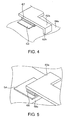
- Fig. 4 shows an example of a technique of fixing the inner lead portion and the external terminal portion in a state of being electrically insulated.
- an insulative adhesive 67 is applied between the lower surface of the inner lead portion 62a and the external terminal portion 53 of the resonator package 50.
- the adhesive 67 By the adhesive 67, the inner lead portion 62a and the external terminal portion 53 are insulated.
- the wall portion 62b serves as a spacer that separates the inner lead portion 62a and the external terminal 53, and thereby, the insulation effect can be assured even more.
- Fig. 5 shows an example of a technique of fixing the inner lead portion to the external terminal portion in an electrically coupled state.
- a conductive adhesive 68 is applied between the lower surface of the inner lead portion 63a and the external terminal portion 54 as a ground terminal of the resonator package 50.
- the adhesive 68 By the adhesive 68, the inner lead portion 63a and the external terminal portion 54 are conductively connected.
- the terminal portion 41 of the IC chip 40 is electrically coupled to the inner lead portion 61 a, and the terminal 42 is electrically coupled to the external terminal 52 of the resonator package 50.
- the terminal portion 43 of the IC chip 40 is electrically coupled to the external terminal 55 of the resonator package 50, and the terminal portion 44 is electrically coupled to the inner lead portion 64a.
- terminal portion 45 is electrically coupled to the inner lead portion 62a
- terminal portion 46 is electrically coupled to the inner lead portion 63a.
- conducting wire such as gold wire, for example, as shown in Fig. 2.
- the respective terminals of the resonator package 50 and the respective inner lead portions connected to the piezoelectric resonating element 51 are arranged so as not to be connected but insulated in the fixed positions, and the respective inner lead portions connected to the IC chip 40 are arranged so as to be connected to the respective terminals of the resonator package 50 by wire-bonding.
- the connection to the piezoelectric resonating element is carried out without via the inner lead portions, the stray capacitance can be reduced.
- resin molding is carried out with synthetic resin so as to coat the components except at least outer lead portions 61 b, 64b of the lead portion 61 of Fig. 1.
- This resin molded portion 20 is provided for insulating the respective terminals, the gold wire of the wire bonding or the like and for protecting the internal structure, and can be formed by injecting, for example, epoxy resin as synthetic resin having advantageous formability and insulation capability into a forming die to shape it as shown in the drawings.
- the embodiment is constructed as described above. As shown in Fig. 2, the IC chip 40 is fixed to the rear surface 58 of the resonator package 50, and, to the rear surface 58, the respective inner lead portions 61 a, 62a, 63a, 64a of the lead frame are further fixed. That is, because IC chip 40 and the inner lead portions are fixed onto the same surface of the vibration package 50, the inner lead portions 61a, 62a, 63a, 64a do not project beyond the front surface side of the resonator package 50, and thereby, the thickness of the entire piezoelectric oscillator 30 can be thinner by the thickness of the inner lead portions.
- the region for fixing the respective inner lead portions 61a, 62a, 63a, 64a and the region for fixing the IC chip 40 can be provided suitably on the same surface 58 of the resonator package 50.
- the thickness of the inner lead portions 61 a, 62a, 63a, 64a is absorbed dimensionally in the thickness of the IC chip 40, and thereby, a piezoelectric oscillator having a thin thickness can be formed easily.
- the resonator package 50 is sealed by the metal lid body 59, and the external terminal 54 electrically connected to the lid body 59 is provided on the rear surface 58 of the resonator package 50, the piezoelectric oscillator 30 can be easily shielded.
- the external terminal 52 and the external terminal 55 connected to the piezoelectric resonating element 51 accommodated therein are provided, and the inner lead portions 61a, 64a are electrically coupled to these terminals.
- the electrical connections of the piezoelectric resonating element 51, the IC chip 40, and the piezoelectric oscillator 30 to the external side can be easily carried out.
- the lead portion 61 and lead portion 64 are bent downwardly from the respective inner lead portions 61a, 64a, which are fixed to the resonator package 50, and the midway positions 61c, 64c are formed so as to extend along the side surface of the piezoelectric oscillator 30.
- the solder is likely to adhere to the respective midway portions 61 c, 64c of the lead portions, respectively, to form fins 69, 69.
- the mounting structure can be reinforced.
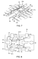
- Fig. 6 is a flowchart briefly explaining an example of the manufacturing process of the piezoelectric oscillator 30.
- a semiconductor device having a built-in oscillating circuit for example, a commercially available IC chip
- a lead frame for forming inner lead portions for example, a quartz package accommodating a quartz resonating element are prepared.
- the IC chip is not limited to that of a commercially available prescribed type, but may be a custom-build chip. Because the position of the external terminal is different when the type is different, the electrical coupling needs to be adapted as described later.
- the lead frame As for the lead frame, a lead frame generally used when manufacturing a package device is used, and a lead frame formed by an Fe alloy such as a 42 alloy or a Cu alloy such as Cu-Sn, Cu-Fe, Cu-Zn, Cu-Ni, or a ternary alloy in which a third element is added thereto, for example, is used.
- the quartz package is the same as the resonator package 50 illustrated in detail in Fig. 3, and the structure thereof is as described above. That is, the package is manufactured by forming necessary electrodes in the ceramic package, for example, bonding the piezoelectric resonating element 51, and then sealing air-tightly by the lid body 59. Subsequently, the resonator package 50 as the quartz package is subjected to a unit inspection, as required, for its vibration frequency or the like (ST11), and followed by the next step.
- ST11 vibration frequency or the like
- Fig. 7 shows a state in which inner lead portions of the lead frame are fixed onto the rear surface 58 of the resonator package (ST12).
- the number of the inner lead portions fixed onto the rear surface 58 of the resonator package is not limited to the number illustrated in Fig. 2, but a large number of lead portions can be fixed as shown by the signs of 60-1, 60-2.
- auxiliary lead portions 65, 66 which are arranged in a direction different from the direction in which these inner lead portions extend, for example, in a direction perpendicular to the direction in which the large number of inner lead portions denoted by 60-1, 60-2 extend, to the rear surface 58 of the resonator package, the large number of inner lead portions can be fixed while holding them not to displace.
- the IC chip 40 is fixed substantially at the center of the rear surface 58 of the resonator package 50 with an adhesive or the like (ST13).
- the terminal portions of the IC chip 40 and the external terminal portions 52, 53, 54, 55 of the resonator package and the large number of inner lead portions 60-1, 60-2 are electrically coupled by wire-bonding (ST14).
- the arrangement is placed within a forming die (not shown), and the resin molded portion 20 described in Figs. 1 and 2 is formed by resin molding by injecting mold resin into the die (ST15). Then, using a prescribed jig the bending structures of the lead portions 61, 64 shown in Fig. 1 are shaped, and thus, the piezoelectric oscillator 30 including predetermined outer lead portions 61 b, 64b is formed (ST16). Subsequently, necessary inspection is performed (ST17), and the oscillator is packed (ST18) to bring it into the condition that it can be shipped as a product.
- Fig. 8 is a schematic plan view showing a second embodiment of the piezoelectric oscillator of the invention. Because the parts assigned with the same signs as used in the first embodiment are common, overlapping description will be omitted, and the difference will be mainly described below.
- the piezoelectric oscillator 70 of this second embodiment is different in construction of an IC chip 40-1 to be fixed to the rear surface 58 of the resonator package 50. That is, as compared to Fig. 2, the IC chip 40 and the IC chip 40-1 are different in the arrangement of their terminal portions.
- the input/output terminal 41 and connection terminals 42, 43 to the resonator package 50 are arranged along the left end side of the IC chip 40, which is the same as with the embodiment.
- the difference is in the point that the control terminal 44 is disposed near to the center of the upper end side of the IC chip 40-1 as shown in Fig. 8.
- the output terminal 45 and the ground terminal 46 are arranged along the right end side of the IC chip 40-1 in Fig. 8.
- the same terminal as the external terminal portion 55 of the first embodiment is provided as a first external terminal portion 55-1 in the same position as in the first embodiment, and further, a second external terminal portion 55-2 electrically connected to the first external terminal portion 55-1 within the package is exposed near to the right of the lower end side of the resonator package 50 in Fig. 8.
- a third external terminal 55-3 electrically connected to the second external terminal portion 55-2 within the package is exposed near to the right of the upper end side of the resonator package 50 in Fig. 8.
- the connection terminal 43 of the IC chip 40-1 is connected to the first external terminal portion 55-1 of the resonator package 50 by wire-bonding or the like
- the inner lead portion 64a is connected to the second external terminal portion 55-2 by wire-bonding or the like
- the connection terminal 44 of the IC chip 40-1 is connected to the third external terminal portion 55-3 of the resonator package 50 by wire-bonding or the like.
- the necessary electrical coupling between the IC chip 40-1 and the resonator package 50 can be carried out by wire-bonding the respective connection terminals of the IC chip 40-1 to the external terminal portions and the inner lead portion arranged on the periphery thereof. That is, by exposing the necessary number of terminals connected to the piezoelectric resonating element 51 on the rear surface 58 of the resonator package 50, the IC chip having a different terminal arrangement can be used.
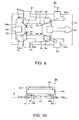
- Fig. 9 is a schematic plan view showing a third embodiment of the piezoelectric oscillator of the invention. Because the parts assigned with the same signs as used in the first embodiment are common, overlapping description will be omitted, and the difference will be mainly described as below.
- the piezoelectric oscillator 90 of this third embodiment is mainly different from the first embodiment in the positions and forms of the inner lead portions 61 a, 62a, 63a, 64a.
- the inner lead portions 61 a, 62a, 63a, 64a are arranged so as not to overlap two-dimensionally with the external terminal portions 52, 55, which are electrically coupled to the piezoelectric resonating element 51 within the resonator package 50.
- arrangement of the inner lead portions 61 a, 62a, 63a, 64a are two-dimensionally shifted so that the respective principal surfaces thereof may not overlap with the principal surfaces of the external terminal portions 52, 55, and the inner lead portions 61 a, 62a, 63a, 64a may not contact the external terminal portions 52, 55.
- the inner lead portions 61 a, 64a have notch portions 61 d, 64d so as to take a longer distance to the external terminal portions 52, 55 in the horizontal direction within the limited range of the rear surface 58 of the resonator package 50.
- the notch portions 61 d, 64d are formed so as to have forms that avoid the outline of the adjacent external terminal portions 52, 55 as shown in the drawing.
- the inner lead portions 62a, 63a may be arranged so as to overlap two-dimensionally with the external terminal portions 53, 54.
- the inner lead portions 62a, 63a are arranged so as not to overlap two-dimensionally with the external terminal portions 53, 54 in order to suppress the thickness of the piezoelectric oscillator 90.
- the inner lead portions 61a, 64a are arranged so as not to overlap two-dimensionally with the external terminal portions 52, 55, respectively, in order to avoid the contact with the external terminal portions 52, 55, unlike the first embodiment, there is no need to use the insulative adhesive 67 (see Fig. 4) for fixing them to the rear surface 58 of the resonator package 50, and a conductive adhesive may also be used.
- the piezoelectric oscillator 90 according to the third embodiment of the invention is constructed as described above, and thereby, exerts the same operation and effect as those in the first embodiment.
- the inner lead portions 61a, 62a, 63a, 64a are arranged so as not to overlap two-dimensionally with the external terminal portions 52, 55. Thereby, the respective distances between the inner lead portions 61 a, 64a and the external terminal portions 52, 55 can be larger than in the first embodiment, the electrical insulation between the inner lead portions 61 a, 64a and the external terminal portions 52, 55 can be more assured, and the stray capacitance can be made smaller.
- the inner lead portions 61a, 64a have the notch portions 61d, 64d, the distances between the end surfaces of the inner lead portions 61 a, 64a and the end surfaces of the external terminal portions 52, 55 can be made even larger, the electrical insulation between the inner lead portions 61a, 64a and the external terminal portions 52, 55 can be even more assured, and the stray capacitance can be made even smaller.
- the terminal portion 44 of the IC chip 40 in Fig. 9 is disposed near the inner lead portion 64a.
- Fig. 10 is a schematic side view showing a fourth embodiment of the piezoelectric oscillator of the invention. Because the parts assigned with the same signs as used in the first embodiment are common, overlapping description will be omitted, and the difference will be mainly described as below.
- the piezoelectric oscillator 80 of this fourth embodiment is different in forms of the lead portions to be fixed to the rear surface 58 of the resonator package 50. Further, the coating range of the resin molded portion 20-1 is different. That is, the region at the center part of the lid body 59 of the resonator package 50 is exposed form the resin molded portion 20-1. Thereby, only the IC chip 40, the inner lead portions 61 a, 64a, side surfaces of the resonator package 50, and the bonded region of the resonator package 50 and the lid body 59 are resin molded.
- the lid body 59 of the resonator package 50 is exposed form the resin molded portion 20-1, the heat dissipation of the heat generated by driving the semiconductor constituting the oscillating circuit can be accelerated.
- frequency adjustment can be carried out by applying a laser beam or the like via the lid body to the internal piezoelectric resonating element (not shown).
- the resonator package 50 is disposed with the rear surface 58 directed downward, which is reverse to that in the case of Fig. 1, and the respective lead portions 61, 64 fixed to the downward rear surface 58 are shorter than those in the case of Fig. 1, and bent in the form of a crank.
- the respective lead portions do not have the structures that project to the sides and come toward the mounting substrate K along the side surfaces of the resonator package 50 as in the case of Fig. 1, the size in the width direction becomes smaller than that of the piezoelectric oscillator 30 in Fig. 1. Accordingly, the mounting space can also be made smaller than that of the piezoelectric oscillator 30 in Fig. 1.
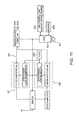
- Fig. 11 shows a schematic constitution of a digital portable telephone unit 300 as an example of electronic equipment applying the piezoelectric oscillator according to the above described embodiments of the invention.
- the voice of a transmitter converted into an electric signal by a microphone 308 is digitally modulated in a demodulator/codec unit, and frequency converted to an RF (Radio Frequency) band in the transmitting unit 307, and then, transmitted via an antenna to the base station (not shown).
- RF Radio Frequency
- RF signals from the base station are frequency converted in the receiving unit 306, and converted into an audio signal in the demodulator/codec unit, and then, output from a speaker 309.
- a CPU (Central Processing Unit) 301 controls the entire operation of the telephone unit 300 including an input/output unit 302 having a liquid crystal display device and a keyboard.
- a memory 303 is information storage means including a RAM, ROM controlled by the CPU 301, and a control program of the telephone unit 300 and information such as a telephone directory are stored therein.
- TCXO Tempoture Compensated X'stal Oscillator
- the TCXO 305 is a piezoelectric oscillator in which the frequency variation due to ambient temperature change is reduced, and is widely used in portable telephone units as a frequency reference source of the receiving unit 306 and the transmitting unit 307 in Fig. 11. Because the demand for miniaturization of the TCXO 305 becomes higher with the recent miniaturization of the portable telephone units, the miniaturization of the TCXO by the structure according to the embodiments of the invention is extremely effective.
Landscapes
- Engineering & Computer Science (AREA)
- General Engineering & Computer Science (AREA)
- Mechanical Engineering (AREA)
- Oscillators With Electromechanical Resonators (AREA)
- Piezo-Electric Or Mechanical Vibrators, Or Delay Or Filter Circuits (AREA)
Description
- The present invention relates to a piezoelectric oscillator, including a piezoelectric resonator package accommodating a piezoelectric resonating element and a semiconductor device having a built-in oscillating circuit for oscillating the piezoelectric resonating element.
- In compact information equipment such as an HDD (Hard Disk Drive), a mobile computer, or an IC card, and mobile communication equipment such as a portable telephone, a car phone, or a paging system, a piezoelectric oscillator is widely used within the package. Conventionally, in the structure of a piezoelectric oscillator, a piezoelectric resonator unit and an oscillating circuit unit are respectively constituted by separate packages, and, for example, a structure in which the package constituting the piezoelectric resonator unit is overlapped with the package constituting the oscillating circuit unit and fixed thereon has been known (Microfilm of Publication of Utility Model Application No. H02-4312). Such structure can avoid various disadvantages when the piezoelectric resonating element and the oscillating circuit are accommodated within the same package. That is, there are some cases where gas, generated when resin cures, adheres to the piezoelectric resonating element and that leads to degradation, if the piezoelectric resonating element and the oscillating circuit are accommodated within the same package.
- Therefore, as described above, by accommodating the piezoelectric resonating element and the oscillating circuit in separate packages, and overlapping them in the longitudinal direction, these disadvantages can be avoided and the oscillator can be constructed smaller. By the way, recently, in various equipment equipped with a piezoelectric oscillator, further miniaturization becomes a challenge, and thus, the piezoelectric oscillator itself is needed to be formed smaller.
- Therefore, the piezoelectric oscillator having the constitution in which the piezoelectric resonating element and the oscillating circuit are accommodated in separate packages and overlapped in the longitudinal direction as described above is constructed, for example, as shown in Fig. 12.
- Fig. 12 is a schematic perspective view showing the above described conventional piezoelectric oscillator in the middle of the manufacturing process. In the drawing, a lead frame 1 is fixed onto one
surface 2a of aresonator package 2 accommodating a piezoelectric resonating element therein. The lead frame 1 includes adevice mounting portion 4, and anIC chip 3 is fixed onto thedevice mounting portion 4. The respective terminals of theIC chip 3 are wire-bonded to pluralinner lead portions 5 included in the lead frame 1 using bonding wires 6. - However, in the piezoelectric oscillator as in Fig. 11, because the lead frame 1 is fixed onto the one
surface 2a of theresonator package 2, and theIC chip 3 is fixed onto thedevice mounting portion 4 of the lead frame 1, the entire thickness becomes larger. - The document
JP 11-284 441 A -
JP 04-259 104 A -
US 5,541,557 A discloses a resin mold type piezoelectric oscillator, in which a resonator package is mounted on one side and a semiconductor device is mounted on the other side of a center portion of a lead frame. Terminals of the resonator package are bent towards and connected to lead portions of the lead frame. Terminals on a surface of the semiconductor device that faces away from the lead frame are wire-bonded to lead portions of the lead frame. - An object of the present invention is to provide a small piezoelectric oscillator that has a small stray capacitance.
- This object is achieved by a piezoelectric oscillator as claimed in claim 1. Preferred embodiments of the invention are subject-matter of the dependent claims.
- According to the construction of a first embodiment of the invention, the semiconductor device having the built-in oscillating circuit is fixed onto the rear surface of the resonator package, and the inner lead portion of the lead frame is further fixed onto the rear surface. Because the semiconductor device and the inner lead portion are fixed onto the same surface of the resonator package, and the inner lead portion does not project toward the front surface side of the resonator package by the thickness thereof, the entire thickness can be made thinner by the thickness of the inner lead portion. Thereby, as an advantage of the invention, a piezoelectric oscillator, in which the size in the thickness direction can be made smaller and the space required for mounting can be made smaller than those in the prior art, can be provided.
- Preferred embodiments of the invention will be explained below with reference to the drawings, in which:
- Fig. 1
- is a schematic side view showing a first embodiment of a piezoelectric oscillator of the invention;
- Fig. 2
- is a schematic plan view of the piezoelectric oscillator in Fig. 1;
- Fig. 3
- is a schematic sectional view along line A-A of Fig. 2;
- Fig. 4
- is a schematic perspective view showing an example of a technique of fixing the inner lead portion and the external terminal portion of the piezoelectric oscillator in Fig. 1 in a state of being electrically insulated;
- Fig. 5
- is a schematic perspective view showing an example of a technique of fixing the piezoelectric oscillator in Fig. 1 in a state of being electrically coupled;
- Fig. 6
- is a flowchart simply showing an example of the manufacturing process of the piezoelectric oscillator in Fig. 1;
- Fig. 7
- is a schematic perspective view showing a part of the process of Fig. 6;
- Fig. 8
- is a schematic plan view showing a second embodiment of the piezoelectric oscillator of the invention;
- Fig. 9
- is a schematic plan view showing a third embodiment of the piezoelectric oscillator of the invention;
- Fig. 10
- is a schematic side view showing a fourth embodiment of the piezoelectric oscillator of the invention;
- Fig. 11
- is a view showing a schematic constitution of a digital portable telephone unit as an example of electronic equipment applying the piezoelectric oscillator according to the embodiments of the invention; and
- Fig. 12
- is a schematic perspective view showing a part of the manufacturing process of a conventional piezoelectric oscillator.
- Figs. 1 to 3 show a first embodiment of a piezoelectric oscillator of the invention. Fig. 1 is a schematic side view (left side view) of the piezoelectric oscillator, Fig. 2 is a schematic plan view of the piezoelectric oscillator, and Fig. 3 is a schematic sectional view along line A-A of Fig. 2. Note that, in Fig. 1, the internal construction is shown by making a resin molded portion transparent for convenience of understanding.
- In the drawings, a
piezoelectric oscillator 30 includes aresonator package 50 accommodating a piezoelectric resonating element, and anIC chip 40 that is a semiconductor device fixed to the rear surface of theresonator package 50 and having a built-in oscillating circuit. - As shown in Fig. 3, the
resonator package 50 is formed by laminating plural base plates, formed by shaping ceramic green sheets of aluminum oxide, for example, as an insulating material, and then sintering them. - Some base plates are provided with holes so as to form a predetermined internal space S1 inside when laminated, and the package is in the form of an opened rectangular box. A piezoelectric
resonating element 51 is accommodated in the internal space S1. That is, as shown in Fig. 3, electrode portions 56 (only one being visible), formed by, for example, nickel plating and gold plating on metallized tungsten, are provided so as to be exposed to the internal space S1 near the left end of the bottom of the resonator package 50 (the top and bottom is reversely shown in Fig. 3). Twoelectrode portions 56 of the same form are formed near both ends in the width direction of theresonator package 50 in Fig. 2 (in the direction perpendicular to the drawing sheet). - The
electrode portions 56 in Fig. 3 are connected to externalterminal portions resonator package 50. Theelectrode portions 56 are electrically coupled to theIC chip 40, in a manner as described later, to supply a driving voltage to the piezoelectricresonating element 51. That is, as shown in Fig. 3, aconductive adhesive 57 is applied to the surface of theelectrode portions 56, and a lead electrode portion (not shown) of abase portion 51 a of the piezoelectric resonatingelement 51 is mounted on the surface of theconductive adhesive 57 and bonded by curing theconductive adhesive 57. - By the way, as for the
conductive adhesive 57, an adhesive made by including conductive particles, such as fine silver particles, in a synthetic resin agent as an adhesive component that exerts bonding force can be used, and silicone, epoxy, or polyimide conductive adhesives or the like can be used. Thepiezoelectric resonating element 51 is formed from quartz, for example; alternatively, a piezoelectric material such as lithium tantalate and lithium niobate can be used. In the case of the embodiment, as for the piezoelectric resonatingelement 51, for example, a so-called AT cut resonating element formed by cutting a quartz wafer into rectangular shape along a prescribed direction or a resonating element in the form of a tuning fork can be used. - The
piezoelectric resonating element 51 is provided with two excitation electrodes as the electrodes for driving, and the above described lead electrode, connected to the excitation electrode and formed by leading on the bonding end of the piezoelectric resonatingelement 51 on the surface thereof. - In Fig. 3, a
lid body 59 is for air-tightly sealing thepiezoelectric resonating element 51 within the internal space S1, and a plate-formed lid body is used in the embodiment. By using a wax material (not shown), thelid body 59 is fixed to the open end of theresonator package 50 to seal it. As for thelid body 59, conductive metal such as a metallic alloy of Fe-Ni-Co is preferably used. The lid body is connected, by aconductive portion 53a, to anexternal terminal portion 53, on therear surface 58 of the resonator package 50 (the front side surface shown in Fig. 2 and the top surface in Fig. 3). - Further, in Fig. 2, an
external terminal portion 54, exposed on therear surface 58 of theresonator package 50 is also connected to thelid body 59 by the same structure. In the embodiment, with the structure described as below, a shield effect can be provided by grounding thelid body 59 using theexternal terminal 54. - Next, the
IC chip 40 as a semiconductor device is for accommodating the oscillating circuit formed by an integrated circuit (not shown) inside thereof. TheIC chip 40 is fixed to therear surface 58 of the resonator package 50 (the front side surface shown in Fig. 2 and the top surface in Fig. 3) near the center thereof using an epoxy or silicon adhesive, for example. In this case, as shown in Fig. 2, therear surface 58 of theresonator package 50 has a larger area than the bonded surface of theIC chip 40, and forms an exposedsurface 58a around the periphery of theIC chip 40. On the surface of theIC chip 40, which is opposite to the bonded surface of theresonator package 50, several terminal portions are provided, and sixterminal portions 41 to 46 are exposed in Fig. 2. Needless to say, there are some cases where the number of terminal portions is larger or smaller than six depending on type of the IC chip. - in the embodiment shown in Fig. 2, the
terminal portions IC chip 40 are connection terminals to theresonator package 50, for example. Theterminal portion 41 is an input/output terminal of the oscillating circuit. Theterminal portion 44 is a control terminal, the terminal portion 45 is an output terminal, and theterminal portion 46 is a ground terminal. The input/output terminal 41, theconnection terminals resonator package 50, and thecontrol terminal 44 are arranged along the left end side of theIC chip 40 in Fig. 2. On the other hand, the output terminal 45 and theground terminal 46 are arranged along the right end side of theIC chip 40 in Fig. 2. - Further, as shown in Figs. 1 and 2, in the positions that overlap with the external
terminal portions rear surface 58 of theresonator package 50,inner lead portions lead portions inner lead portion 61 a is a power supply terminal of thepiezoelectric oscillator 30, theinner lead portion 62a is an output terminal of thepiezoelectric oscillator 30, theinner lead portion 63a is a ground terminal of thepiezoelectric oscillator 30, and theinner lead portion 64a is a control terminal of thepiezoelectric oscillator 30. Of the respective inner lead portions, theinner lead portions terminal portions inner lead portion 63a is fixed in a state of being electrically connected to theexternal terminal portion 54 as a ground terminal of theresonator package 50. Additionally, as for the embodiment shown in Fig. 1, of thelead portions inner lead portions outer lead portions - Further, in Fig. 2, substantially at the center in the width direction of the
resonator package 50,auxiliary lead portions resonator package 50 in the manufacturing process are fixed to the right and left positions in the drawing. - Fig. 4 shows an example of a technique of fixing the inner lead portion and the external terminal portion in a state of being electrically insulated. In the drawing, an
insulative adhesive 67 is applied between the lower surface of theinner lead portion 62a and theexternal terminal portion 53 of theresonator package 50. By the adhesive 67, theinner lead portion 62a and theexternal terminal portion 53 are insulated. In this case, preferably, by integrally forming awall portion 62b extending from theinner lead portion 62a toward the resonator package side, thewall portion 62b serves as a spacer that separates theinner lead portion 62a and theexternal terminal 53, and thereby, the insulation effect can be assured even more. - Fig. 5 shows an example of a technique of fixing the inner lead portion to the external terminal portion in an electrically coupled state. In the drawing, a
conductive adhesive 68 is applied between the lower surface of theinner lead portion 63a and theexternal terminal portion 54 as a ground terminal of theresonator package 50. By the adhesive 68, theinner lead portion 63a and theexternal terminal portion 54 are conductively connected. - Further, as shown in Fig. 2, the
terminal portion 41 of theIC chip 40 is electrically coupled to theinner lead portion 61 a, and the terminal 42 is electrically coupled to theexternal terminal 52 of theresonator package 50. In addition, theterminal portion 43 of theIC chip 40 is electrically coupled to theexternal terminal 55 of theresonator package 50, and theterminal portion 44 is electrically coupled to theinner lead portion 64a. - Furthermore, the terminal portion 45 is electrically coupled to the
inner lead portion 62a, and theterminal portion 46 is electrically coupled to theinner lead portion 63a. These electrical connections are carried out by wire-bonding using conducting wire such as gold wire, for example, as shown in Fig. 2. - Therefore, the respective terminals of the
resonator package 50 and the respective inner lead portions connected to thepiezoelectric resonating element 51 are arranged so as not to be connected but insulated in the fixed positions, and the respective inner lead portions connected to theIC chip 40 are arranged so as to be connected to the respective terminals of theresonator package 50 by wire-bonding. On this account, because the connection to the piezoelectric resonating element is carried out without via the inner lead portions, the stray capacitance can be reduced. - After such electrical coupling is carried out, resin molding is carried out with synthetic resin so as to coat the components except at least outer
lead portions lead portion 61 of Fig. 1. This resin moldedportion 20 is provided for insulating the respective terminals, the gold wire of the wire bonding or the like and for protecting the internal structure, and can be formed by injecting, for example, epoxy resin as synthetic resin having advantageous formability and insulation capability into a forming die to shape it as shown in the drawings. - The embodiment is constructed as described above. As shown in Fig. 2, the
IC chip 40 is fixed to therear surface 58 of theresonator package 50, and, to therear surface 58, the respectiveinner lead portions IC chip 40 and the inner lead portions are fixed onto the same surface of thevibration package 50, theinner lead portions resonator package 50, and thereby, the thickness of the entirepiezoelectric oscillator 30 can be thinner by the thickness of the inner lead portions. - Specifically, because the construction in which the
rear surface 58 of theresonator package 50 has a larger area than the bonded surface of theIC chip 40 fixed to therear surface 58, and the respectiveinner lead portions surface 58a, which is exposed in the state in which theIC chip 40 is fixed to therear surface 58 of theresonator package 50, the region for fixing the respectiveinner lead portions IC chip 40 can be provided suitably on thesame surface 58 of theresonator package 50. Thereby, it is assured that the thickness of theinner lead portions IC chip 40, and thereby, a piezoelectric oscillator having a thin thickness can be formed easily. Further, because theresonator package 50 is sealed by themetal lid body 59, and theexternal terminal 54 electrically connected to thelid body 59 is provided on therear surface 58 of theresonator package 50, thepiezoelectric oscillator 30 can be easily shielded. In addition, on therear surface 58 of theresonator package 50, theexternal terminal 52 and theexternal terminal 55 connected to thepiezoelectric resonating element 51 accommodated therein are provided, and theinner lead portions element 51, theIC chip 40, and thepiezoelectric oscillator 30 to the external side can be easily carried out. - Further, as shown in Fig. 1, the
lead portion 61 andlead portion 64 are bent downwardly from the respectiveinner lead portions resonator package 50, and themidway positions piezoelectric oscillator 30. On this account, in the case where the mounting is carried out on a mounting substrate K or the like using solder as shown in the drawings, the solder is likely to adhere to the respectivemidway portions fins - Fig. 6 is a flowchart briefly explaining an example of the manufacturing process of the
piezoelectric oscillator 30. As shown in the drawing, at first, as a semiconductor device having a built-in oscillating circuit, for example, a commercially available IC chip, a lead frame for forming inner lead portions, and, as theresonator package 50, for example, a quartz package accommodating a quartz resonating element are prepared. The IC chip is not limited to that of a commercially available prescribed type, but may be a custom-build chip. Because the position of the external terminal is different when the type is different, the electrical coupling needs to be adapted as described later. As for the lead frame, a lead frame generally used when manufacturing a package device is used, and a lead frame formed by an Fe alloy such as a 42 alloy or a Cu alloy such as Cu-Sn, Cu-Fe, Cu-Zn, Cu-Ni, or a ternary alloy in which a third element is added thereto, for example, is used. The quartz package is the same as theresonator package 50 illustrated in detail in Fig. 3, and the structure thereof is as described above. That is, the package is manufactured by forming necessary electrodes in the ceramic package, for example, bonding thepiezoelectric resonating element 51, and then sealing air-tightly by thelid body 59. Subsequently, theresonator package 50 as the quartz package is subjected to a unit inspection, as required, for its vibration frequency or the like (ST11), and followed by the next step. - Fig. 7 shows a state in which inner lead portions of the lead frame are fixed onto the
rear surface 58 of the resonator package (ST12). As shown in the drawing, the number of the inner lead portions fixed onto therear surface 58 of the resonator package is not limited to the number illustrated in Fig. 2, but a large number of lead portions can be fixed as shown by the signs of 60-1, 60-2. In this case, by fixingauxiliary lead portions rear surface 58 of the resonator package, the large number of inner lead portions can be fixed while holding them not to displace. Then, theIC chip 40 is fixed substantially at the center of therear surface 58 of theresonator package 50 with an adhesive or the like (ST13). Next, as shown in the drawing, the terminal portions of theIC chip 40 and the externalterminal portions - In such state, the arrangement is placed within a forming die (not shown), and the resin molded
portion 20 described in Figs. 1 and 2 is formed by resin molding by injecting mold resin into the die (ST15). Then, using a prescribed jig the bending structures of thelead portions piezoelectric oscillator 30 including predetermined outerlead portions - Fig. 8 is a schematic plan view showing a second embodiment of the piezoelectric oscillator of the invention. Because the parts assigned with the same signs as used in the first embodiment are common, overlapping description will be omitted, and the difference will be mainly described below.
- The
piezoelectric oscillator 70 of this second embodiment is different in construction of an IC chip 40-1 to be fixed to therear surface 58 of theresonator package 50. That is, as compared to Fig. 2, theIC chip 40 and the IC chip 40-1 are different in the arrangement of their terminal portions. In the IC chip 40-1, the input/output terminal 41 andconnection terminals resonator package 50 are arranged along the left end side of theIC chip 40, which is the same as with the embodiment. - However, the difference is in the point that the
control terminal 44 is disposed near to the center of the upper end side of the IC chip 40-1 as shown in Fig. 8. In addition, the output terminal 45 and theground terminal 46 are arranged along the right end side of the IC chip 40-1 in Fig. 8. In response to the difference in construction of the IC chip 40-1, on therear surface 58 of theresonator package 50, the same terminal as theexternal terminal portion 55 of the first embodiment is provided as a first external terminal portion 55-1 in the same position as in the first embodiment, and further, a second external terminal portion 55-2 electrically connected to the first external terminal portion 55-1 within the package is exposed near to the right of the lower end side of theresonator package 50 in Fig. 8. - Moreover, a third external terminal 55-3 electrically connected to the second external terminal portion 55-2 within the package is exposed near to the right of the upper end side of the
resonator package 50 in Fig. 8. In this case, as shown in the drawing, theconnection terminal 43 of the IC chip 40-1 is connected to the first external terminal portion 55-1 of theresonator package 50 by wire-bonding or the like, theinner lead portion 64a is connected to the second external terminal portion 55-2 by wire-bonding or the like, and theconnection terminal 44 of the IC chip 40-1 is connected to the third external terminal portion 55-3 of theresonator package 50 by wire-bonding or the like. - Thereby, as in the first embodiment, the necessary electrical coupling between the IC chip 40-1 and the
resonator package 50 can be carried out by wire-bonding the respective connection terminals of the IC chip 40-1 to the external terminal portions and the inner lead portion arranged on the periphery thereof. That is, by exposing the necessary number of terminals connected to thepiezoelectric resonating element 51 on therear surface 58 of theresonator package 50, the IC chip having a different terminal arrangement can be used. - Fig. 9 is a schematic plan view showing a third embodiment of the piezoelectric oscillator of the invention. Because the parts assigned with the same signs as used in the first embodiment are common, overlapping description will be omitted, and the difference will be mainly described as below.
- The
piezoelectric oscillator 90 of this third embodiment is mainly different from the first embodiment in the positions and forms of theinner lead portions - That is, in the
piezoelectric oscillator 90, theinner lead portions terminal portions piezoelectric resonating element 51 within theresonator package 50. Specifically, arrangement of theinner lead portions terminal portions inner lead portions terminal portions - Further, the
inner lead portions notch portions 61 d, 64d so as to take a longer distance to the externalterminal portions rear surface 58 of theresonator package 50. Thenotch portions 61 d, 64d are formed so as to have forms that avoid the outline of the adjacent externalterminal portions - Note that the
inner lead portions terminal portions inner lead portions terminal portions piezoelectric oscillator 90. - In addition, because the
inner lead portions terminal portions terminal portions rear surface 58 of theresonator package 50, and a conductive adhesive may also be used. Thepiezoelectric oscillator 90 according to the third embodiment of the invention is constructed as described above, and thereby, exerts the same operation and effect as those in the first embodiment. - Further, the
inner lead portions terminal portions inner lead portions terminal portions inner lead portions terminal portions - Especially, in Fig. 9, because the
inner lead portions notch portions 61d, 64d, the distances between the end surfaces of theinner lead portions terminal portions inner lead portions terminal portions - By the way, the
terminal portion 44 of theIC chip 40 in Fig. 9 is disposed near theinner lead portion 64a. On this account, there is no need to provide the external terminal portions 55-2, 55-3 in theresonator package 50 and connect these external terminal portions and theinner lead portion 64a as in Fig. 8 in the second embodiment, and the stray capacitance can be made smaller as compared to thepiezoelectric oscillator 70 in Fig. 8. - Fig. 10 is a schematic side view showing a fourth embodiment of the piezoelectric oscillator of the invention. Because the parts assigned with the same signs as used in the first embodiment are common, overlapping description will be omitted, and the difference will be mainly described as below.
- The
piezoelectric oscillator 80 of this fourth embodiment is different in forms of the lead portions to be fixed to therear surface 58 of theresonator package 50. Further, the coating range of the resin molded portion 20-1 is different. That is, the region at the center part of thelid body 59 of theresonator package 50 is exposed form the resin molded portion 20-1. Thereby, only theIC chip 40, theinner lead portions resonator package 50, and the bonded region of theresonator package 50 and thelid body 59 are resin molded. - By such construction, because the most part of the
lid body 59 of theresonator package 50 is exposed form the resin molded portion 20-1, the heat dissipation of the heat generated by driving the semiconductor constituting the oscillating circuit can be accelerated. Further, in the case where thelid body 59 is formed from a light transmissive material such as glass, by not covering thelid body 59 with resin, frequency adjustment can be carried out by applying a laser beam or the like via the lid body to the internal piezoelectric resonating element (not shown). - In addition, in Fig. 10, the
resonator package 50 is disposed with therear surface 58 directed downward, which is reverse to that in the case of Fig. 1, and therespective lead portions rear surface 58 are shorter than those in the case of Fig. 1, and bent in the form of a crank. Thereby, because the respective lead portions do not have the structures that project to the sides and come toward the mounting substrate K along the side surfaces of theresonator package 50 as in the case of Fig. 1, the size in the width direction becomes smaller than that of thepiezoelectric oscillator 30 in Fig. 1. Accordingly, the mounting space can also be made smaller than that of thepiezoelectric oscillator 30 in Fig. 1. - Fig. 11 shows a schematic constitution of a digital
portable telephone unit 300 as an example of electronic equipment applying the piezoelectric oscillator according to the above described embodiments of the invention. In the drawing, the voice of a transmitter converted into an electric signal by amicrophone 308 is digitally modulated in a demodulator/codec unit, and frequency converted to an RF (Radio Frequency) band in the transmittingunit 307, and then, transmitted via an antenna to the base station (not shown). - RF signals from the base station are frequency converted in the receiving
unit 306, and converted into an audio signal in the demodulator/codec unit, and then, output from aspeaker 309. A CPU (Central Processing Unit) 301 controls the entire operation of thetelephone unit 300 including an input/output unit 302 having a liquid crystal display device and a keyboard. Amemory 303 is information storage means including a RAM, ROM controlled by theCPU 301, and a control program of thetelephone unit 300 and information such as a telephone directory are stored therein. As for an application of the piezoelectric oscillator according to the embodiments of the invention, for example, there is a TCXO (Temperature Compensated X'stal Oscillator) 305. - The
TCXO 305 is a piezoelectric oscillator in which the frequency variation due to ambient temperature change is reduced, and is widely used in portable telephone units as a frequency reference source of the receivingunit 306 and the transmittingunit 307 in Fig. 11. Because the demand for miniaturization of theTCXO 305 becomes higher with the recent miniaturization of the portable telephone units, the miniaturization of the TCXO by the structure according to the embodiments of the invention is extremely effective. - As described above, using the
piezoelectric oscillator portable telephone unit 300 makes the size in the width direction smaller, which contributes to the entire miniaturization of thetelephone unit 300.
Claims (6)
- A piezoelectric oscillator, comprising:a resonator package (50) accommodating a piezoelectric resonating element (51) and having first terminals (52, 55) provided on a rear surface thereof, the first terminals being connected to the piezoelectric resonating element (51); anda semiconductor device (40) having second terminals (42, 43) on one surface thereof, wherein the semiconductor device (40) is fixed onto said rear surface of the resonator package (50) and has a built-in oscillating circuit, andinner lead portions (61 a, 62a, 63a, 64a) of a lead frame that are fixed to said rear surface (58) of the resonator package (50) so as to be insulated from the first terminals,wherein said first terminals are connected to corresponding ones of said second terminals, and the resonator package (50) and the semiconductor device (40) are resin molded except for an outer lead portion (61, 62, 63, 64) of the lead frame,
characterized in that
said semiconductor device (40) is fixed to said rear surface (58) of the resonator package (50) such that said one surface of the semiconductor device (40) faces away from said rear surface (58) of the resonator package (50); and
said first terminals (52, 55) are connected by wire-bonding to said corresponding second terminals (42, 43) to be connected to the oscillating circuit of the semiconductor device (40). - The oscillator according to Claim 1, wherein the rear surface (58) of the resonator package (50) has a larger area than the surface of the semiconductor device (40) fixed onto the rear surface (58), and the inner lead portions (61 a, 62a, 63a, 64a) are fixed to the rear surface (58) at a surface portion outside of the contact area between the rear surface of the resonator package (50) and the semiconductor device (40).
- The oscillator according to Claims 1 or 2, wherein said inner lead portions (61a, 64a) insulated from said first terminals (52, 55) are arranged so as not to overlap with the first terminals (52, 55-1) in plan view.
- The oscillator according to Claim 3, wherein an inner lead portion (69 a, 64a) of said inner lead portions (61 a, 64a) insulated from said first terminals (52, 55) is arranged juxtaposed to a terminal of said first terminals and has a notch portion facing that so as to increase the distance between the inner lead portion (61 a, 64a) and the juxtaposed first terminal (52, 55-1).
- The oscillator according to any one of Claims 1, 2 or 3, wherein the resonator package (50) is sealed by a metal lid body (59), and a terminal (53) conductively connected to the lid body (59) is provided on the rear surface (58) of the resonator package (50), and this terminal and an inner lead portion (62a) of the lead frame connected to the semiconductor device (40) are electrically coupled and fixed through contact with each other.
- The piezoelectric oscillator according to claim 5, wherein the piezoelectric oscillator is resin molded except for a region at the center part of the lid body (59) of the resonator package (50).
Applications Claiming Priority (4)
| Application Number | Priority Date | Filing Date | Title |
|---|---|---|---|
| JP2003068323 | 2003-03-13 | ||
| JP2003068323 | 2003-03-13 | ||
| JP2004001219A JP4314999B2 (en) | 2003-03-13 | 2004-01-06 | Piezoelectric oscillator, mobile phone device using piezoelectric oscillator, and electronic device using piezoelectric oscillator |
| JP2004001219 | 2004-01-06 |
Publications (2)
| Publication Number | Publication Date |
|---|---|
| EP1458086A1 EP1458086A1 (en) | 2004-09-15 |
| EP1458086B1 true EP1458086B1 (en) | 2007-10-17 |
Family
ID=32775275
Family Applications (1)
| Application Number | Title | Priority Date | Filing Date |
|---|---|---|---|
| EP04005790A Expired - Lifetime EP1458086B1 (en) | 2003-03-13 | 2004-03-11 | Piezoelectric Oscillator |
Country Status (7)
| Country | Link |
|---|---|
| US (1) | US7057331B2 (en) |
| EP (1) | EP1458086B1 (en) |
| JP (1) | JP4314999B2 (en) |
| KR (1) | KR100645637B1 (en) |
| CN (1) | CN1531190B (en) |
| DE (1) | DE602004009490T2 (en) |
| TW (1) | TW200428753A (en) |
Families Citing this family (33)
| Publication number | Priority date | Publication date | Assignee | Title |
|---|---|---|---|---|
| US7830074B2 (en) * | 2006-08-08 | 2010-11-09 | Hrl Laboratories, Llc | Integrated quartz oscillator on an active electronic substrate |
| US7994877B1 (en) | 2008-11-10 | 2011-08-09 | Hrl Laboratories, Llc | MEMS-based quartz hybrid filters and a method of making the same |
| US8766745B1 (en) | 2007-07-25 | 2014-07-01 | Hrl Laboratories, Llc | Quartz-based disk resonator gyro with ultra-thin conductive outer electrodes and method of making same |
| JP4852850B2 (en) * | 2005-02-03 | 2012-01-11 | セイコーエプソン株式会社 | Piezoelectric vibration element, piezoelectric vibrator, piezoelectric oscillator, frequency stabilization method, and piezoelectric vibrator manufacturing method |
| JP2006245098A (en) * | 2005-03-01 | 2006-09-14 | Seiko Epson Corp | Electronic component and manufacturing method thereof, and electronic apparatus |
| US20070045640A1 (en) * | 2005-08-23 | 2007-03-01 | Erchak Alexei A | Light emitting devices for liquid crystal displays |
| JP2006311380A (en) * | 2005-04-28 | 2006-11-09 | Epson Toyocom Corp | Piezoelectric vibrator and piezoelectric oscillator |
| JP4534912B2 (en) * | 2005-08-30 | 2010-09-01 | 株式会社デンソー | Angular velocity sensor mounting structure |
| JP2007173431A (en) * | 2005-12-21 | 2007-07-05 | Epson Toyocom Corp | Piezoelectric device |
| JP2007189380A (en) * | 2006-01-12 | 2007-07-26 | Epson Toyocom Corp | Piezoelectric device and electronic equipment |
| JP4742938B2 (en) * | 2006-03-29 | 2011-08-10 | エプソントヨコム株式会社 | Piezoelectric device and manufacturing method thereof |
| JP4765004B2 (en) * | 2006-09-04 | 2011-09-07 | 富士電機株式会社 | Semiconductor device and manufacturing method thereof |
| JP2008259004A (en) * | 2007-04-06 | 2008-10-23 | Epson Toyocom Corp | Piezoelectric device and manufacturing method thereof |
| US10266398B1 (en) | 2007-07-25 | 2019-04-23 | Hrl Laboratories, Llc | ALD metal coatings for high Q MEMS structures |
| US7876168B2 (en) * | 2007-12-14 | 2011-01-25 | Epson Toyocom Corporation | Piezoelectric oscillator and method for manufacturing the same |
| US8151640B1 (en) | 2008-02-05 | 2012-04-10 | Hrl Laboratories, Llc | MEMS on-chip inertial navigation system with error correction |
| US7802356B1 (en) | 2008-02-21 | 2010-09-28 | Hrl Laboratories, Llc | Method of fabricating an ultra thin quartz resonator component |
| JP2010147850A (en) * | 2008-12-19 | 2010-07-01 | Nippon Dempa Kogyo Co Ltd | Crystal oscillator for surface mounting |
| JP2010190706A (en) * | 2009-02-18 | 2010-09-02 | Panasonic Corp | Inertial force sensor |
| US8176607B1 (en) | 2009-10-08 | 2012-05-15 | Hrl Laboratories, Llc | Method of fabricating quartz resonators |
| US8912711B1 (en) | 2010-06-22 | 2014-12-16 | Hrl Laboratories, Llc | Thermal stress resistant resonator, and a method for fabricating same |
| JP5281175B1 (en) * | 2012-04-27 | 2013-09-04 | ラピスセミコンダクタ株式会社 | Semiconductor device and measuring instrument |
| US9230890B2 (en) | 2012-04-27 | 2016-01-05 | Lapis Semiconductor Co., Ltd. | Semiconductor device and measurement device |
| CN104079249B (en) | 2013-03-27 | 2018-05-04 | 精工爱普生株式会社 | Electronic device, electronic equipment, moving body, the manufacture method of electronic device |
| US9599470B1 (en) | 2013-09-11 | 2017-03-21 | Hrl Laboratories, Llc | Dielectric high Q MEMS shell gyroscope structure |
| JP2015089102A (en) * | 2013-09-24 | 2015-05-07 | 日本電波工業株式会社 | Oscillator |
| US9977097B1 (en) | 2014-02-21 | 2018-05-22 | Hrl Laboratories, Llc | Micro-scale piezoelectric resonating magnetometer |
| US9991863B1 (en) | 2014-04-08 | 2018-06-05 | Hrl Laboratories, Llc | Rounded and curved integrated tethers for quartz resonators |
| US10308505B1 (en) | 2014-08-11 | 2019-06-04 | Hrl Laboratories, Llc | Method and apparatus for the monolithic encapsulation of a micro-scale inertial navigation sensor suite |
| US10031191B1 (en) | 2015-01-16 | 2018-07-24 | Hrl Laboratories, Llc | Piezoelectric magnetometer capable of sensing a magnetic field in multiple vectors |
| US10175307B1 (en) | 2016-01-15 | 2019-01-08 | Hrl Laboratories, Llc | FM demodulation system for quartz MEMS magnetometer |
| JP6276338B2 (en) * | 2016-07-25 | 2018-02-07 | ラピスセミコンダクタ株式会社 | Semiconductor device and measuring instrument |
| JP6493995B2 (en) * | 2017-05-25 | 2019-04-03 | ラピスセミコンダクタ株式会社 | Semiconductor device and measuring instrument |
Family Cites Families (14)
| Publication number | Priority date | Publication date | Assignee | Title |
|---|---|---|---|---|
| US5392006A (en) * | 1987-02-27 | 1995-02-21 | Seiko Epson Corporation | Pressure seal type piezoelectric resonator |
| JPH01135214A (en) | 1987-11-20 | 1989-05-26 | Matsushima Kogyo Co Ltd | Piezo-oscillator |
| JPH024312U (en) | 1988-06-20 | 1990-01-11 | ||
| JP3099382B2 (en) * | 1991-02-14 | 2000-10-16 | セイコーエプソン株式会社 | Small oscillator |
| JPH04334202A (en) | 1991-05-10 | 1992-11-20 | Seiko Epson Corp | Piezoelectric oscillator |
| US5912592A (en) * | 1994-07-04 | 1999-06-15 | Seiko Epson Corporation | Piezoelectric oscillator |
| JP3421747B2 (en) | 1995-02-15 | 2003-06-30 | セイコーエプソン株式会社 | Piezoelectric oscillator and voltage controlled oscillator |
| JPH11284441A (en) | 1998-03-30 | 1999-10-15 | Nippon Dempa Kogyo Co Ltd | Manufacture of temperature compensated crystal oscillator |
| US6229249B1 (en) * | 1998-08-31 | 2001-05-08 | Kyocera Corporation | Surface-mount type crystal oscillator |
| TW569424B (en) * | 2000-03-17 | 2004-01-01 | Matsushita Electric Ind Co Ltd | Module with embedded electric elements and the manufacturing method thereof |
| US6703768B2 (en) * | 2000-09-27 | 2004-03-09 | Citizen Watch Co., Ltd. | Piezoelectric generator and mounting structure therefor |
| US6456168B1 (en) * | 2000-12-29 | 2002-09-24 | Cts Corporation | Temperature compensated crystal oscillator assembled on crystal base |
| US6833654B2 (en) * | 2002-09-25 | 2004-12-21 | Cts Corporation | Dual crystal package |
| JP4222147B2 (en) * | 2002-10-23 | 2009-02-12 | セイコーエプソン株式会社 | Piezoelectric oscillator, mobile phone device using piezoelectric oscillator, and electronic device using piezoelectric oscillator |
-
2004
- 2004-01-06 JP JP2004001219A patent/JP4314999B2/en not_active Expired - Fee Related
- 2004-03-09 TW TW093106204A patent/TW200428753A/en not_active IP Right Cessation
- 2004-03-11 DE DE602004009490T patent/DE602004009490T2/en not_active Expired - Lifetime
- 2004-03-11 EP EP04005790A patent/EP1458086B1/en not_active Expired - Lifetime
- 2004-03-11 US US10/797,196 patent/US7057331B2/en active Active
- 2004-03-12 KR KR1020040016910A patent/KR100645637B1/en not_active IP Right Cessation
- 2004-03-12 CN CN2004100086070A patent/CN1531190B/en not_active Expired - Fee Related
Also Published As
| Publication number | Publication date |
|---|---|
| US20040245895A1 (en) | 2004-12-09 |
| KR20040081381A (en) | 2004-09-21 |
| CN1531190B (en) | 2010-05-26 |
| DE602004009490T2 (en) | 2008-07-31 |
| US7057331B2 (en) | 2006-06-06 |
| JP4314999B2 (en) | 2009-08-19 |
| JP2004297770A (en) | 2004-10-21 |
| TW200428753A (en) | 2004-12-16 |
| CN1531190A (en) | 2004-09-22 |
| DE602004009490D1 (en) | 2007-11-29 |
| TWI303923B (en) | 2008-12-01 |
| EP1458086A1 (en) | 2004-09-15 |
| KR100645637B1 (en) | 2006-11-13 |
Similar Documents
| Publication | Publication Date | Title |
|---|---|---|
| EP1458086B1 (en) | Piezoelectric Oscillator | |
| EP1489736B1 (en) | Piezoelectric oscillator, manufacturing method therefor, mobile phone apparatus using piezoelectric oscillator, and electronic apparatus using piezoelectric oscillator | |
| US6518501B1 (en) | Electronic part and method of assembling the same | |
| TWI314812B (en) | ||
| US6998926B2 (en) | Piezoelectric oscillator, portable phone employing piezoelectric oscillator, and electronic apparatus employing piezoelectric oscillator | |
| JP2006050529A (en) | Piezoelectric oscillator and its manufacturing method | |
| JP3418373B2 (en) | Surface acoustic wave device and method of manufacturing the same | |
| CN100492880C (en) | Piezoelectric oscillator and electronic equipment and method for producing piezoelectric oscillator | |
| JPH0818390A (en) | Surface acoustic wave device | |
| JP2004297554A (en) | Piezoelectric oscillator, portable telephone and electronic device using it | |
| US6876264B2 (en) | Surface-mount crystal oscillator | |
| JP5097929B2 (en) | Manufacturing method of electronic parts | |
| JP2005341045A (en) | Piezoelectric oscillator | |
| JP5024317B2 (en) | Electronic component and method for manufacturing electronic component | |
| JPH10163798A (en) | Surface acoustic wave element and electronic part using the same | |
| JP2002330050A (en) | Hollow resin mold surface acoustic wave filter | |
| JP2007097075A (en) | Piezoelectric oscillator and method for manufacturing the same | |
| JPH11307664A (en) | Electronic package component and manufacture thereof | |
| JPS6112231B2 (en) |
Legal Events
| Date | Code | Title | Description |
|---|---|---|---|
| PUAI | Public reference made under article 153(3) epc to a published international application that has entered the european phase |
Free format text: ORIGINAL CODE: 0009012 |
|
| AK | Designated contracting states |
Kind code of ref document: A1 Designated state(s): AT BE BG CH CY CZ DE DK EE ES FI FR GB GR HU IE IT LI LU MC NL PL PT RO SE SI SK TR |
|
| AX | Request for extension of the european patent |
Extension state: AL LT LV MK |
|
| 17P | Request for examination filed |
Effective date: 20050303 |
|
| 17Q | First examination report despatched |
Effective date: 20050404 |
|
| AKX | Designation fees paid |
Designated state(s): CH DE FR GB LI |
|
| GRAP | Despatch of communication of intention to grant a patent |
Free format text: ORIGINAL CODE: EPIDOSNIGR1 |
|
| GRAS | Grant fee paid |
Free format text: ORIGINAL CODE: EPIDOSNIGR3 |
|
| GRAA | (expected) grant |
Free format text: ORIGINAL CODE: 0009210 |
|
| AK | Designated contracting states |
Kind code of ref document: B1 Designated state(s): CH DE FR GB LI |
|
| REG | Reference to a national code |
Ref country code: GB Ref legal event code: FG4D |
|
| REG | Reference to a national code |
Ref country code: CH Ref legal event code: EP Ref country code: CH Ref legal event code: NV Representative=s name: E. BLUM & CO. AG PATENT- UND MARKENANWAELTE VSP |
|
| REF | Corresponds to: |
Ref document number: 602004009490 Country of ref document: DE Date of ref document: 20071129 Kind code of ref document: P |
|
| ET | Fr: translation filed | ||
| PLBE | No opposition filed within time limit |
Free format text: ORIGINAL CODE: 0009261 |
|
| STAA | Information on the status of an ep patent application or granted ep patent |
Free format text: STATUS: NO OPPOSITION FILED WITHIN TIME LIMIT |
|
| 26N | No opposition filed |
Effective date: 20080718 |
|
| REG | Reference to a national code |
Ref country code: FR Ref legal event code: PLFP Year of fee payment: 13 |
|
| PGFP | Annual fee paid to national office [announced via postgrant information from national office to epo] |
Ref country code: CH Payment date: 20160311 Year of fee payment: 13 Ref country code: DE Payment date: 20160308 Year of fee payment: 13 |
|
| PGFP | Annual fee paid to national office [announced via postgrant information from national office to epo] |
Ref country code: GB Payment date: 20160309 Year of fee payment: 13 Ref country code: FR Payment date: 20160208 Year of fee payment: 13 |
|
| REG | Reference to a national code |
Ref country code: DE Ref legal event code: R119 Ref document number: 602004009490 Country of ref document: DE |
|
| REG | Reference to a national code |
Ref country code: CH Ref legal event code: PL |
|
| GBPC | Gb: european patent ceased through non-payment of renewal fee |
Effective date: 20170311 |
|
| REG | Reference to a national code |
Ref country code: FR Ref legal event code: ST Effective date: 20171130 |
|
| PG25 | Lapsed in a contracting state [announced via postgrant information from national office to epo] |
Ref country code: FR Free format text: LAPSE BECAUSE OF NON-PAYMENT OF DUE FEES Effective date: 20170331 Ref country code: DE Free format text: LAPSE BECAUSE OF NON-PAYMENT OF DUE FEES Effective date: 20171003 |
|
| PG25 | Lapsed in a contracting state [announced via postgrant information from national office to epo] |
Ref country code: CH Free format text: LAPSE BECAUSE OF NON-PAYMENT OF DUE FEES Effective date: 20170331 Ref country code: LI Free format text: LAPSE BECAUSE OF NON-PAYMENT OF DUE FEES Effective date: 20170331 Ref country code: GB Free format text: LAPSE BECAUSE OF NON-PAYMENT OF DUE FEES Effective date: 20170311 |