WO2025142017A1 - カメラ装置およびカメラ装置の製造方法 - Google Patents
カメラ装置およびカメラ装置の製造方法 Download PDFInfo
- Publication number
- WO2025142017A1 WO2025142017A1 PCT/JP2024/035705 JP2024035705W WO2025142017A1 WO 2025142017 A1 WO2025142017 A1 WO 2025142017A1 JP 2024035705 W JP2024035705 W JP 2024035705W WO 2025142017 A1 WO2025142017 A1 WO 2025142017A1
- Authority
- WO
- WIPO (PCT)
- Prior art keywords
- space
- main board
- camera device
- board
- connector
- Prior art date
- Legal status (The legal status is an assumption and is not a legal conclusion. Google has not performed a legal analysis and makes no representation as to the accuracy of the status listed.)
- Pending
Links
Images


Classifications
-
- G—PHYSICS
- G03—PHOTOGRAPHY; CINEMATOGRAPHY; ANALOGOUS TECHNIQUES USING WAVES OTHER THAN OPTICAL WAVES; ELECTROGRAPHY; HOLOGRAPHY
- G03B—APPARATUS OR ARRANGEMENTS FOR TAKING PHOTOGRAPHS OR FOR PROJECTING OR VIEWING THEM; APPARATUS OR ARRANGEMENTS EMPLOYING ANALOGOUS TECHNIQUES USING WAVES OTHER THAN OPTICAL WAVES; ACCESSORIES THEREFOR
- G03B17/00—Details of cameras or camera bodies; Accessories therefor
- G03B17/02—Bodies
- G03B17/08—Waterproof bodies or housings
-
- G—PHYSICS
- G03—PHOTOGRAPHY; CINEMATOGRAPHY; ANALOGOUS TECHNIQUES USING WAVES OTHER THAN OPTICAL WAVES; ELECTROGRAPHY; HOLOGRAPHY
- G03B—APPARATUS OR ARRANGEMENTS FOR TAKING PHOTOGRAPHS OR FOR PROJECTING OR VIEWING THEM; APPARATUS OR ARRANGEMENTS EMPLOYING ANALOGOUS TECHNIQUES USING WAVES OTHER THAN OPTICAL WAVES; ACCESSORIES THEREFOR
- G03B30/00—Camera modules comprising integrated lens units and imaging units, specially adapted for being embedded in other devices, e.g. mobile phones or vehicles
-
- H—ELECTRICITY
- H04—ELECTRIC COMMUNICATION TECHNIQUE
- H04N—PICTORIAL COMMUNICATION, e.g. TELEVISION
- H04N23/00—Cameras or camera modules comprising electronic image sensors; Control thereof
- H04N23/50—Constructional details
- H04N23/51—Housings
Definitions
- the present invention relates to an in-vehicle camera device and a method for manufacturing the camera device.
- Patent Document 1 An in-vehicle camera comprising a circuit board, a camera case that houses and arranges the circuit board, and a connector portion for external connection provided on the outer surface of the camera case, the connector portion comprising a connector housing integrally formed with the outer surface of the camera case, a connector terminal that is inserted into the outer wall of the camera case and is electrically connected to the circuit board, and a sealant filled between the connector terminal and the connector housing.”
- the connector housing is integrally formed with the camera case, and the gap between the connector housing and the connector terminals electrically connected to the circuit board housed in the camera case is filled with a sealant, thereby making the camera case and connector housing, and the connector housing and connector terminals waterproof.
- a camera device includes a camera module having an imaging board with an imaging element and a lens, a main board with an image processing circuit mounted thereon and connected to the camera module via a communication line, a connector with a connection terminal connected to a connector connection part of the main board, and a housing having a base part and a cover part connected to each other, and housing the camera module and the main board, the housing having a first space in which at least a part of the camera module and the main board are housed, and a second space separated from the first space by a partition wall in which a board area including the connector connection part of the main board is housed, and a sealant is arranged in the second space so as to enclose the board area.
- the present invention makes it possible to improve the vibration resistance and reliability of an in-vehicle camera device while ensuring waterproofing.
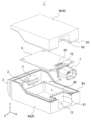
- FIG. 1 is an exploded perspective view of a camera device according to a first embodiment.
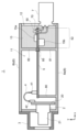
- FIG. FIG. 11 is a cross-sectional view of a camera device according to a modified example.
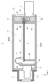
- FIG. 11 is a cross-sectional view of a camera device according to a second embodiment.
- FIG. 11 is a cross-sectional view of a camera device according to a third embodiment.
- 1A to 1C are diagrams illustrating an assembly procedure for the camera device.
- FIG. 1 is an exploded perspective view of the camera device 1.
- Figure 2 is a cross-sectional view of the camera device 1.
- the camera device 1 is an in-vehicle camera device, and is mounted on, for example, a two-wheeled vehicle.
- the camera device 1 includes a camera module 2, a camera cover 3, a main board 5, a connector 7, and a housing 8 that houses the camera module 2 and the main board 5.
- the camera module 2 comprises an imaging board 20 equipped with an imaging element (not shown), and an imaging optical system 21 having an optical lens mounted on a lens barrel.
- the camera module 2 is adhesively fixed or screwed to a mounting portion (not shown) provided on the base portion 8a of the housing 8.
- the imaging optical system 21 is attached to the base portion 8a so that it is exposed outside the housing.
- the camera cover 3 is a cover that protects the imaging optical system 21 exposed outside the housing, and is attached to the base portion 8a.
- the camera cover 3 and the housing 8 are fixed via a waterproof adhesive or a waterproof O-ring.
- the main board 5 is placed on a fixing portion 80 and a partition wall 81 provided on the base portion 8a, and is fixed by screwing into the fixing portion 80. By screwing the main board 5 into the fixing portion 80, the main board 5 is in close contact with the partition wall 81.
- a connector 7 for connecting to an external device is provided in a board area 52 at the right end of the main board 5 in the figure.
- the portion of the board area 52 where the connection terminal 70 of the connector 7 is soldered will be referred to as the connector connection portion 50.
- the connection terminal 70 extending downward from the main board 5 in the figure is bent 90 degrees to the right in the figure from the middle, so that the connector 7 faces to the right.
- FIG. 3 is a cross-sectional view of the camera device 1 according to the modified example.
- the opening of the second space 12 faces the negative y-direction side.
- the connection terminal 70 connected to the connector connection part 50 of the main board 5 is a straight terminal that is not bent. Therefore, the connector 7 also faces the negative y-direction side.
- the opening of the second space 12 is provided on the bottom side of the base portion 8a (the bottom side of the housing 8 in the figure), but it may be provided on the side side of the housing 8 (in a direction perpendicular to the paper) or on the top side of the housing 8 in the figure (the cover portion 8b side), and the connection direction of the connector 7 may be set in those directions.
- the same effect as in the first embodiment described above is achieved, and by changing the position of the opening of the second space 12, the placement space (space in the xz plane) for the camera device 1 can be made smaller, and the degree of freedom in the layout of the camera device when mounted on various vehicles is improved.
- Second Embodiment Fig. 4 is a diagram for explaining the second embodiment, and is a cross-sectional view of the camera device 1, similar to Fig. 2. The following will mainly explain configurations that are different from the first embodiment, and will not explain the same configurations.
- the connector connection portion 50 is arranged in the board area 52 included in the second space 12.
- electronic components are also arranged in the board area 52 included in the second space 12.
- two electronic components 15a and 15b are arranged. These electronic components 15a and 15b are also sealed with the sealant 13 filled in the second space 12.
- the sealant 13 is filled in the second space 12 by placing the housing 8 (base portion 8a and cover portion 8b) in a position where the connector 7 faces upward, and filling the sealant 13 into both the space of the base portion 8a and the space of the cover portion 8b from the opening of the second space 12.
- the sealant 13 seals the board area 52 including the electronic components 15a and 15b and the connector connection portion 50.
- electronic components 15a, 15b that are vulnerable to vibration are provided in board area 52 on the main board 5 and are accommodated on the second space 12 side. Since the second space 12 is filled with sealing material 13, electronic components 15a, 15b are also sealed by sealing material 13, and the stress on electronic components 15a, 15b can be reduced.
- some of the electronic components mounted on the main board 5 are also housed in the second space 12 and enclosed by the sealing material 13. This not only improves the waterproofing performance of the second space 12, but also improves the earthquake resistance of the connector connection portion 50 and the reliability of the electronic components 15a, 15b, which are sensitive to vibration.
- Third Embodiment Fig. 5 is a diagram for explaining the third embodiment, and is a cross-sectional view of the camera device 1 similar to the case of Fig. 2 described above. The following mainly describes configurations different from the first embodiment, and explanations of the same configurations are omitted.
- a buffer material 90 is arranged at least one between the partition 81 and the main board 5 and between the partition 82 and the main board 5.
- the buffer material 90 is arranged both between the partition 81 and the main board 5 and between the partition 82 and the main board 5.
- the partitions 81 and 82 are in direct contact with the main board 5 to separate the spaces.
- gaps may occur between the partitions 81 and 82 and the main board 5.
- the uncured sealant 13 has high fluidity, if a gap occurs between the partitions 81 and 82 and the main board 5, the uncured sealant 13 may flow into the first space 11 through the gap. Therefore, even if a specified amount of sealant 13 is filled in the second space 12, the sealant 13 may flow into the first space 11, resulting in an insufficient amount of sealant 13 in the second space 12, which may result in a decrease in waterproofing.
- the sealant 13 that has flowed into the first space 11 may adhere to electronic components stored on the first space 11 side, causing contact failure and affecting optical components.
- the cushioning material 90 is provided between both the partition walls 81, 82 and the main board 5, but it may be provided only on one side.
- the screw fixation brings the main board 5 and the partition wall 81 into close contact, thereby reducing gaps that occur due to manufacturing tolerances. Therefore, it is possible to apply a configuration in which the cushioning material 90 is provided only between the partition wall 82 and the main board 5, which is preferable from the viewpoint of reducing costs.
- the material for the cushioning material 90 is preferably one that reduces the stress on the main board 5 when it comes into contact with the board.
- a rubber gasket such as ethylene propylene rubber, butadiene rubber, or silicone rubber, a lower elasticity elastomer, or a liquid gasket (low elasticity adhesive, waterproof adhesive) can be used. From the viewpoint of manufacturability, a waterproof adhesive is preferable.
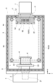
- the thick two-dot chain line represents the waterproof adhesive 9.
- the waterproof adhesive 9 is placed (applied) using, for example, a dispenser, in the groove 84 of the base portion 8a and in the area connected to the partition 82 on the main board 5.
- the two-dot chain line drawn on the partition 81 shown in dashed line represents the waterproof adhesive 9 used to connect the partition 82 of the cover portion 8b to the main board 5, and also functions as the cushioning material 90 mentioned above.
- the waterproof adhesive 9 By using the same material (waterproof adhesive) for the cushioning material 90 and the waterproof adhesive 9 for connecting the housing, continuous application work can be performed in one process, as shown by the two-dot chain line in Figure 6. In other words, the placement of the cushioning material 90 and the waterproof adhesive 9 can be performed continuously, simplifying the manufacturing process.
- the waterproof adhesive 9 As shown by the thick two-dot chain line, the waterproof adhesive 9 can be easily applied continuously and integrally by roughly matching the height of the application surface of the base portion 8a and the application surface of the main board 5.
- the waterproof adhesive 9 can be applied evenly around the entire circumference in one process without interrupting the dispenser discharge.
- the same waterproof adhesive 9 is used for the adhesive used to connect the base portion 8a and the cover portion 8b and for the cushioning material in the partitions 81 and 82, and the manufacturing process can be simplified by continuously applying the waterproof adhesive 9 used for the connection and the waterproof adhesive 9 used for the cushioning material. Furthermore, by roughly matching the height of the application surface of the base portion 8a and the application surface of the main board 5, the waterproof adhesive 9 can be applied uniformly.
- the configuration of the sealing material 13 in the second space 12 is the same as in the first embodiment, and the same effects as in the first embodiment can be achieved.
- the camera device 1 includes a camera module 2 having an imaging board 20 with an imaging element and a lens, a main board 5 with an image processing circuit mounted thereon and connected to the camera module 2 via a communication line 4, a connector 7 with a connection terminal 70 connected to a connector connection portion 50 of the main board 5, and a housing 8 having a base portion 8a and a cover portion 8b connected to each other, and housing the camera module 2 and the main board 5.
- the housing 8 includes a first space 11 in which at least a part of the camera module 2 and the main board 5 are housed, and a second space 12 separated from the first space 11 by a partition (partitions 81 and 82) and housing a board area 52 including the connector connection portion 50 of the main board 5, and a sealant 13 is arranged in the second space 12 to enclose the board area 52.
- the sealing material 13 can be disposed in the second space 12 without affecting the lens of the camera module 2 housed in the first space 11 or the connection portion of the communication line 4.
- the sealing material 13 so as to enclose the board area 52, i.e., so as to enclose the connector connection portion 50 to which the connection terminal 70 of the connector 7 is connected, the stress applied to the connector connection portion 50 can be reduced.
- the partitions (81, 82) are formed by connecting the first partition (partition 81) of the base portion 8a and the second partition (partition 82) of the cover portion 8b, and the substrate area 52 is disposed in the second space 12 by penetrating the connection boundary 85 between the partitions 81 and 82.
- the substrate area 52 By disposing the substrate area 52 in the second space 12 by penetrating the connection boundary 85 between the partitions 81 and 82, it becomes easy to separate the first space 11, which houses the image processing circuit and communication lines 4 mounted on the main substrate 5, from the second space 12 by the partitions 81, 82.
- a deformable cushioning material 90 is provided between at least one of the first partition (partition 81) and the second partition (partition 82) and the main board 5.
Landscapes
- Physics & Mathematics (AREA)
- General Physics & Mathematics (AREA)
- Engineering & Computer Science (AREA)
- Multimedia (AREA)
- Signal Processing (AREA)
- Structure And Mechanism Of Cameras (AREA)
- Studio Devices (AREA)
- Camera Bodies And Camera Details Or Accessories (AREA)
Abstract
カメラ装置は、撮像素子が搭載された撮像基板とレンズとを有するカメラモジュールと、通信線を介してカメラモジュールに接続されるメイン基板と、コネクタ接続部に接続されるコネクタと、ベース部およびカバー部を有し、カメラモジュールおよびメイン基板を収容する筐体と、を備える。筐体は、カメラモジュールの少なくとも一部およびメイン基板が収容される第1空間と、隔壁により第1空間から隔てられ基板領域が収容される第2空間と、を有し、第2空間には、基板領域を内包するように封止材が配置されている。
Description
本発明は、車載のカメラ装置およびカメラ装置の製造方法に関する。
本技術分野の背景技術として、特開2007-001334号公報(特許文献1)がある。この公報には、「回路基板と、前記回路基板を収容配設するカメラケースと、前記カメラケースの外表面に設けられた外部接続用のコネクタ部とを備え、前記コネクタ部は、前記カメラケースの外表面に一体形成されたコネクタハウジングと、前記コネクタハウジング内に収容される様にして前記カメラケースの外壁に貫設され、前記回路基板と電気接続されたコネクタ端子と、前記コネクタ端子と前記コネクタハウジングとの間に充填された封止剤と、を備えることを特徴とする車載カメラ。」と記載されている。
近年、安全意識の高まりから車載カメラの2輪車への搭載が検討されており、車載カメラに対してより高い耐振動・耐衝撃性能が求められている。また、2輪車用のカメラ装置は車外に搭載されるので、防水性が必要とされる。特許文献1に記載の車載カメラでは、コネクタハウジングをカメラケースと一体形成し、カメラケースに収容された回路基板に電気的に接続されたコネクタ端子とコネクタハウジングの間を封止材で充填することで、カメラケースとコネクタハウジング、及びコネクタハウジングとコネクタ端子の防水性を持たせている。
しかしながら、この構造では、例えばコネクタ部に応力がかかった際に、一体形成したカメラケースから破損する可能性や、基板とコネクタ端子の接続部に応力がかかって接続不良が発生する可能性がある。
本発明の一態様によるカメラ装置は、撮像素子が搭載された撮像基板とレンズとを有するカメラモジュールと、画像処理回路が搭載され、通信線を介して前記カメラモジュールに接続されるメイン基板と、前記メイン基板のコネクタ接続部に接続端子が接続されるコネクタと、互いに接続されるベース部およびカバー部を有し、前記カメラモジュールおよび前記メイン基板を収容する筐体と、を備え、前記筐体は、前記カメラモジュールの少なくとも一部および前記メイン基板が収容される第1空間と、隔壁により前記第1空間から隔てられ、前記メイン基板の前記コネクタ接続部を含む基板領域が収容される第2空間と、を有し、前記第2空間には、前記基板領域を内包するように封止材が配置されている。
本発明によれば、車載用のカメラ装置において、防水性を確保しつつ耐振動性能および信頼性の向上を図ることができる。
<第1の実施形態>
図1,2を参照して、本発明の第1の実施形態に係るカメラ装置について説明する。図1は、カメラ装置1の分解斜視図である。図2は、カメラ装置1の断面図である。カメラ装置1は車載のカメラ装置であって、例えば、2輪車に搭載される。カメラ装置1は、カメラモジュール2、カメラカバー3、メイン基板5およびコネクタ7と、カメラモジュール2およびメイン基板5を収容する筐体8とを備えている。
図1,2を参照して、本発明の第1の実施形態に係るカメラ装置について説明する。図1は、カメラ装置1の分解斜視図である。図2は、カメラ装置1の断面図である。カメラ装置1は車載のカメラ装置であって、例えば、2輪車に搭載される。カメラ装置1は、カメラモジュール2、カメラカバー3、メイン基板5およびコネクタ7と、カメラモジュール2およびメイン基板5を収容する筐体8とを備えている。
図2に示すように、カメラモジュール2は、撮像素子(不図示)を搭載した撮像基板20と、鏡筒に光学レンズを搭載した撮像光学系21とを備える。カメラモジュール2は、筐体8のベース部8aに設けられた取り付け部(不図示)に接着固定またはネジ止めされる。撮像光学系21は筐体外部に露出するようにベース部8aに取り付けられる。カメラカバー3は筐体外部に露出している撮像光学系21を保護するカバーであり、ベース部8aに取り付けられている。なお、図示は省略しているが、カメラカバー3と筐体8とは、防水接着剤または防水用Oリングを介して固定されている。
撮像基板20には、CCDセンサ,CMOSセンサ等の撮像素子の他に、撮像素子の駆動や撮像素子から出力される電気信号に対して所定の処理を行う電子部品(回路)が実装されている。図示は省略するが、メイン基板5には、画像処理やシステム制御を行うCPU、MPU、AGTG等の電子部品(画像処理回路)が実装されている。撮像基板20とメイン基板5とは、通信線4を介して接続されている。通信線4のコネクタ40a,40bには、例えば、プレスフィットコネクタが用いられる。プレスフィットコネクタは、コネクタ筐体に設けられたプレスフィット端子を基板のスルーホールに圧入することで電気的接続を行う、すなわち、はんだ無しに接続を行うコネクタである。
メイン基板5は、ベース部8aに設けられた固定部80および隔壁81上に載置され、固定部80にネジ止めをすることで固定される。メイン基板5を固定部80にネジ止めすることにより、メイン基板5が隔壁81に密着する。図2において、メイン基板5の図示右端の基板領域52には、外部装置と接続されるコネクタ7が設けられている。以下では、基板領域52においてコネクタ7の接続端子70がはんだ接合された部分を、コネクタ接続部50と称することにする。メイン基板5から図示下方に延びる接続端子70は、途中から図示右方向に90度屈曲しており、コネクタ7は右方向を向いている。
メイン基板5を固定部80に固定した後、カバー部8bの凸部83がベース部8aの溝部84に挿入されるようにカバー部8bをベース部8aに固定する。その場合、カバー部8bとベース部8aとは防水接着剤または防水用Oリングを介して固定される。防水接着剤や防水用Oリングは溝部84に配置される。
カバー部8bには、ベース部8aの隔壁81と対向するように隔壁82が形成されている。なお、隔壁81,82は、図1の破線矢印Lで示すように、折れ曲がった形状に形成されている。カバー部8bをベース部8aに固定すると、隔壁81と隔壁82とがメイン基板5を挟むように接続される。その結果、カバー部8bとベース部8aとから成る筐体8の内部には、隔壁81,82で隔てられた第1空間11および第2空間12が形成される。
図2において、隔壁81,82の図示左側の第1空間11には、カメラモジュール2およびメイン基板5の基板領域51が収容される。基板領域51には、画像処理やシステム制御を行う電子部品が搭載される。隔壁81,82の図示右側の第2空間12には、メイン基板5の内のコネクタ接続部50を含む基板領域52が収容される。すなわち、メイン基板5はそのほとんどが第1空間11に収容されるが、図示右端のコネクタ接続部50を含む基板領域52については、隔壁81と隔壁82との接続境界85(破線で示す部分)を貫通して第2空間12に収容される。第2空間12には、封止材13が充填される。封止材13は、コネクタ接続部50を含む基板領域52が内包されるように第2空間12内に充填される。なお、封止材13が充填された後、第2空間12の一部(隅等)に隙間が形成されていてもよい。もちろん、第2空間12の全領域に封止材13を充填するようにしても良い。
カメラ装置1の組み立て手順は、概略、以下のような手順となる。なお、以下では、ベース部8aとカバー部8bとの接続を防水接着剤で行う場合について説明する。コネクタ7が接続されたメイン基板5およびカメラモジュール2のそれぞれを、ベース部8aに取り付ける。メイン基板5を固定部80にネジ固定すると、隔壁81の上端とメイン基板5の裏面とが密着する。
次いで、通信線4により撮像基板20とメイン基板5とを接続し、カメラカバー3を取り付ける。そして、ベース部8aの溝部84(図1参照)に防水接着剤を配置(塗布)し、カバー部8bの隔壁82の先端がメイン基板5の基板面に密着するようにベース部8aとカバー部8bとを接続する。その後、筐体8の姿勢を第2空間12の開口が上側となるような状態にして、第2空間12の開口から封止材13を充填する。図2に示す例では、封止材13は、接続端子70がコネクタ7から突出するコネクタ根元部分(凸状の部分)まで充填されているが、第2空間12に封止材13を充填して、コネクタ7の左側のフランジ状部分まで封止されるようにしても良い。封止材13は、メイン基板5の表面側および裏面側の両方の空間に充填されるので、封止材13の熱膨張によるメイン基板5の変形を防止できる。
封止材13としては、例えば、(a)硬化剤と主剤を混合させて常温で硬化する2液常温硬化タイプ、(b)硬化剤と主剤を混合させて加熱硬化する2液加熱硬化タイプ、(c)1液中に主剤と硬化剤を含み、加熱により硬化剤を反応させる1液硬化タイプなどがある。また、封止材13に用いられる樹脂種類としては、ウレタン、シリコン、エポキシ樹脂などを使用することができる。
製造タクトの観点からは、硬化が早い2液加熱タイプがより好適である。また、耐振動性の観点から、硬化後樹脂の柔軟性が高いウレタンまたはシリコン樹脂の封止材が好適である。低分子シロキサンによる電子部品の接点障害を防ぐために、ウレタン樹脂、または低分子シロキサン成分をカットしたシリコン樹脂が最も好適に用いられる。加熱硬化タイプを使用する場合は、第2空間12に封止材13を充填した後に、硬化炉にて加熱して封止材13を硬化させることで、コネクタ7、ベース部8aおよびカバー部8b間の防水性を発現することができる。
上述のように、隔壁81,82により第1空間11を第2空間12から隔離したので、カメラモジュール2の光学系や通信線4による接続に影響することなく封止材13を第2空間12に配置することができる。すなわち、従来のような封止材13の光学系への影響、すなわち、通信線4に封止材13が付着することによる接続不良、カメラモジュール2の撮像レンズに封止材13が付着することで正しい画像が得られないという不具合、などを防止することができる。例えば、通信線4にプレスフィットコネクタのような差し込み接触によるコネクタを使用する場合、第1空間11に封止材13が浸入すると、差し込み接触部に封止材13が入り込み通信不良を招くおそれがあった。
また、封止材13は隔壁81,82を貫通する基板領域52を内包するように充填されるので、貫通部分の防水性向上を図ることができる。なお、隔壁81,82はメイン基板5の基板面に密着するように配置されているので、封止材充填作業の際に、未硬化状態で流動性の高い封止材13が第2空間12から第1空間11側へ浸入するのを防止することができる。
また、コネクタ接続部50を含む基板領域52が第2空間12に充填された封止材13に内包されることにより、コネクタ7に応力がかかった際に封止材13により応力が分散し、コネクタ接続部50への影響を低減することができる。その結果、耐振動性能の向上を図ることができ、車両に搭載されるカメラ装置1の信頼性向上を図ることができる。
従来、防水性を考慮してコネクタ7のボディを筐体と一体に形成する構成がある。しかし、カメラ装置1を二輪車に搭載した場合、四輪車に搭載した場合と比べて大きな振動や衝撃を受ける。そのため、一体化されているコネクタボディと筐体との境界部分において振動等により亀裂が生じやすく、防水性能が低下する。一方、本実施形態では、上述のように第2空間12に封止材13を充填する構造なので、振動による防水性低下を防止することができる。
(変形例)
次に、第1実施形態の変形例に関して、図3を用いて説明する。図3は、変形例に係るカメラ装置1の断面図である。なお、以下では、上述した図2に示す構成と異なる部分を中心に説明し、同一構成の部分については説明を省略する。変形例では、第2空間12の開口はy方向マイナス側を向いている。メイン基板5のコネクタ接続部50に接続される接続端子70は、図2の場合とは異なり曲がっていない真っすぐな端子になっている。そのため、コネクタ7もy方向マイナス側を向いている。
次に、第1実施形態の変形例に関して、図3を用いて説明する。図3は、変形例に係るカメラ装置1の断面図である。なお、以下では、上述した図2に示す構成と異なる部分を中心に説明し、同一構成の部分については説明を省略する。変形例では、第2空間12の開口はy方向マイナス側を向いている。メイン基板5のコネクタ接続部50に接続される接続端子70は、図2の場合とは異なり曲がっていない真っすぐな端子になっている。そのため、コネクタ7もy方向マイナス側を向いている。
上述した図2に示す構成の場合には、第2空間12の開口は基板領域52の表面側および裏面側の両方に対向している。そのため、第2空間12の開口から封止材13を充填する際に、基板領域52の表面側および裏面側の両方に容易に封止材13を充填することができる。
一方、図3に示す変形例の場合、第2空間12の開口は基板領域52の裏面側にだけ対向している。封止材充填の際には、筐体8を上下反転して第2空間12の開口が上を向く姿勢にし、封止材13を開口から基板領域52の裏面側の空間に充填することになる。そこで、基板領域52の図示右端部と筐体8との隙間120を十分な大きさに設定し、充填の際の隙間120を介したベース部8a側の空間からカバー部8b側の空間への封止材13の移動、および、カバー部8b側の空間からベース部8a側の空間へのエア抜きが容易にできるような構成としている。そのような構成とすることで、気泡の少ない封止材13を第2空間12に充填することができる。
もちろん、隙間120を小さく設定して、第2空間12の基板領域52の裏面側(ベース部8a側の空間)にだけ封止材13をするような構成とすることも可能である。しかし、基板領域52の片側だけに封止材13を充填した場合には、封止材13の熱膨張によってメイン基板5が変形する可能性がある。また、コネクタ接続部50の耐振動性能向上のためには、カバー部8b側の空間へも封止材13を充填するのが望ましい。
なお、図3に示した例では、第2空間12の開口をベース部8aの底面側(筐体8の図示下側)に設けたが、筐体8の側面側(紙面に直交する方向)や筐体8の図示上側(カバー部8b側)に設けて、それらの方向にコネクタ7の接続方向を設定しても良い。変形例では、上述した第1の実施の形態と同様の作用効果を奏すると共に、第2空間12の開口の配置を変えることでカメラ装置1の配置スペース(xz平面におけるスペース)をより小さくでき、また、種々の車両に搭載する際のカメラ装置のレイアウトの自由度が向上する。
<第2の実施形態>
図4は第2の実施形態を説明する図であり、上述した図2の場合と同様にカメラ装置1を断面した図である。以下では、第1の実施形態と異なる構成を中心に説明し、同一構成の部分については説明を省略する。
図4は第2の実施形態を説明する図であり、上述した図2の場合と同様にカメラ装置1を断面した図である。以下では、第1の実施形態と異なる構成を中心に説明し、同一構成の部分については説明を省略する。
メイン基板5において、第2空間12に含まれる基板領域52にはコネクタ接続部50のみが配置されていた。一方、第2の実施形態では、第2空間12に含まれる基板領域52にも電子部品が配置されている。図4に示す例では、二つの電子部品15a,15bが配置されている。そして、これらの電子部品15a,15bも、第2空間12に充填された封止材13により封止されている。なお、第2空間12への封止材13の充填は、第1の実施形態の場合と同様に、筐体8(ベース部8aおよびカバー部8b)をコネクタ7が上向きとなる姿勢にし、第2空間12の開口からベース部8aの空間およびカバー部8bの空間の両方に封止材13を充填する。封止材13は、電子部品15a,15bおよびコネクタ接続部50を含む基板領域52を封止する。
メイン基板5に搭載された電子部品の内、電解コンデンサなどのサイズの大きい電子部品は、振動により基板接続部(はんだ接続部等)に亀裂が生じ、接続不良を起こすことがある。そこで、本実施形態では、電解コンデンサ等振動に弱い電子部品15a,15bをメイン基板5上の基板領域52に設け、第2空間12側に収容するようにした。第2空間12は封止材13が充填されるので電子部品15a,15bも封止材13により封止され、電子部品15a,15bにかかる応力を低減することができる。
上述のように、第2の実施形態では、メイン基板5に搭載される電子部品の一部(電子部品15a,15b)も第2空間12に収容して封止材13で内包される構成とした。それにより、第2空間12に対する防水性能の向上に加え、コネクタ接続部50の耐震性能の向上および振動に弱い電子部品15a,15bの信頼性の向上を図ることができる。
<第3の実施形態>
図5は第3の実施形態を説明する図であり、上述した図2の場合と同様にカメラ装置1を断面した図である。以下では、第1の実施形態と異なる構成を中心に説明し、同一構成の部分については説明を省略する。第3の実施形態では、隔壁81,82の接続境界において、隔壁81とメイン基板5との間および隔壁82とメイン基板5との間の少なくとも一方に、緩衝材90を配置するようにした。なお、図5に示す例では、隔壁81とメイン基板5との間および隔壁82とメイン基板5との間の両方に緩衝材90を配置している。
図5は第3の実施形態を説明する図であり、上述した図2の場合と同様にカメラ装置1を断面した図である。以下では、第1の実施形態と異なる構成を中心に説明し、同一構成の部分については説明を省略する。第3の実施形態では、隔壁81,82の接続境界において、隔壁81とメイン基板5との間および隔壁82とメイン基板5との間の少なくとも一方に、緩衝材90を配置するようにした。なお、図5に示す例では、隔壁81とメイン基板5との間および隔壁82とメイン基板5との間の両方に緩衝材90を配置している。
上述した図2に示す第1の実施形態の構成では、隔壁81,82はメイン基板5と直接に接触することによって空間を隔てている。しかし、メイン基板5、ベース部8aおよびカバー部8bの製造公差によって、隔壁81,82とメイン基板5との間に隙間が生じる可能性がある。未硬化状態の封止材13は流動性が高いので、隔壁81,82とメイン基板5との間に隙間が生じると、その隙間から第1空間11に未硬化状態の封止材13が流れ込む可能性がある。そのため、第2空間12に規定量の封止材13を充填した場合でも、封止材13が第1空間11側に流れ込んで第2空間12の封止材13の量が不十分となり、防水性の低下を招くおそれがある。また、第1空間11に流れ込んだ封止材13が、第1空間11側に収納されている電子部品に付着することによる接点障害や、光学部品への影響が懸念される。
本実施形態では、隔壁81,82とメイン基板5との間に変形可能な緩衝材90を介在させることで、緩衝材90の変形により製造公差による隙間の発生を防止することができる。その結果、第2空間12から第1空間11への未硬化状態の封止材13の流れ込みを防止することができる。
なお、図5に示す例では、緩衝材90を隔壁81,82とメイン基板5との間の両方に設けているが、一方だけに設けるようにしても良い。例えば、上述したようにメイン基板5を固定部80にネジ固定する場合には、ネジ固定によりメイン基板5と隔壁81とが密着することで、製造公差により発生する隙間を減少させることが可能である。そのため、緩衝材90を隔壁82とメイン基板5との間にだけ設ける構成を適用することができ、コスト低減の観点から好適である。
緩衝材90の材料としては、メイン基板5と接触した際の基板への応力を低減させるものが好ましい。例えば、エチレンプロピレンゴムやブタジエンゴム、シリコーンゴム等のゴムガスケットや、より低弾性なエラストマー、液状ガスケット(低弾性接着剤、防水接着剤)が用いられる。製造性の観点を考慮すると、防水接着剤が好適である。
緩衝材90に防水接着剤を用いた場合のカメラ装置1の組み立て手順を、図6を用いて説明する。図6は、カメラモジュール2、カメラカバー3、コネクタ7が接続されたメイン基板5を筐体8のベース部8aに取り付け、通信線4で撮像基板20とメイン基板5とを接続した状態を示す平面図である。なお、メイン基板5において、ハッチングを施した部分が基板領域52である。メイン基板5はベース部8aの固定部80および隔壁81の上に載置され、固定部80にネジ固定されている。メイン基板5のほとんどの領域は第1空間側に配置され、コネクタ接続部50を含む基板領域52だけが隔壁81を越えて第2空間12側に配置されている。
図6において、太い二点鎖線は防水接着剤9を表している。防水接着剤9は、例えばディスペンサ等を用いて、ベース部8aの溝部84、および、メイン基板5上の隔壁82と接続される領域に配置(塗布)される。図6では、破線で示す隔壁81の部分に記載の二点鎖線が、カバー部8bの隔壁82とメイン基板5との接続に用いられる防水接着剤9を表しており、上述した緩衝材90としても機能するものである。このように防水接着剤9を塗布してベース部8aとカバー部8bとの接続を行うことで、筐体8の接続部の防水性を確保するようにしている。
緩衝材90と筐体接続用の防水接着剤9とに同じ材料(防水接着剤)を使用することで、図6の二点鎖線で示すように1工程で連続的な塗布作業を行うことができる。すなわち、緩衝材90および防水接着剤9の配設を連続して行うことができ、製造工程を簡略化することができる。なお、太い二点鎖線で示すように防水接着剤9を塗布する場合、ベース部8aの塗布面とメイン基板5の塗布面との高さ略一致させることにより、容易に防水接着剤9を一体に連続的に塗布することができる。
例えば、図6の符号Cで示す箇所において、ベース部8aの塗布面とメイン基板5の塗布面との間に明らかな段差が有った場合、その段差の所でディスペンサを上下方向(高さ方向)に移動させる工程が必要になる。そのため、その段差部分(符号Cで示す箇所)に余分な接着剤が溜まってしまうことになる。段差部分でそのような状況が生じないようにするためには、ディスペンサをベース部8aからメイン基板5に移動させる際に、防水接着剤9の吐出を一端中断してディスペンサの高さ方向移動を行う必要があり、作業時間増加というデメリットが生じる。
一方、上述のようにベース部8aの塗布面とメイン基板5の塗布面との高さ略一致させることで、ディスペンサの吐出を中断することなく、1工程で全周に亘って防水接着剤9を均一に塗布することができる。
上述のように、ベース部8aとカバー部8bとの接続に用いる接着剤と隔壁81、82における緩衝材とに共通の防水接着剤9を使用し、接続に用いる防水接着剤9と緩衝材に用いる防水接着剤9とを連続して塗布することで、製造工程が簡略化できる。さらに、ベース部8aの塗布面とメイン基板5の塗布面との高さ略一致させることで、防水接着剤9を均一に塗布することができる。なお、第2空間12における封止材13の構成は第1の実施形態と同様であり、第1の実施形態と同様の作用効果を奏することができる。
上述した実施形態および変形例によれば、次の作用効果を奏する。
(1)図1,2等に示すように、カメラ装置1は、撮像素子が搭載された撮像基板20とレンズとを有するカメラモジュール2と、画像処理回路が搭載され、通信線4を介してカメラモジュール2に接続されるメイン基板5と、メイン基板5のコネクタ接続部50に接続端子70が接続されるコネクタ7と、互いに接続されるベース部8aおよびカバー部8bを有し、カメラモジュール2およびメイン基板5を収容する筐体8と、を備える。そして、筐体8は、カメラモジュール2の少なくとも一部およびメイン基板5が収容される第1空間11と、隔壁(隔壁81,82)により第1空間11から隔てられ、メイン基板5のコネクタ接続部50を含む基板領域52が収容される第2空間12と、を有し、第2空間12には、基板領域52を内包するように封止材13が配置されている。
第2空間12を隔壁(隔壁81,82)により第1空間11から隔てたので、第1空間11に収容されたカメラモジュール2のレンズや通信線4の接続部に影響することなく、封止材13を第2空間12に配置することができる。また、基板領域52を内包するように、すなわち、コネクタ7の接続端子70が接続されるコネクタ接続部50を内包するように封止材13を配置することで、コネクタ接続部50にかかる応力を低減することができる。
(2)上記(1)において、図4に示すように、基板領域52には少なくとも一つの電子部品15a,15bが搭載され、封止材13は電子部品15a,15bおよび基板領域52を内包する。電解コンデンサ等のように振動に弱い電子部品15a,15bを封止材13で内包することで電子部品に係る応力を低減することができ、信頼性向上を図ることができる。
(3)上記(1)において、図2等に示すように、隔壁(81,82)は、ベース部8aの第1隔壁(隔壁81)とカバー部8bの第2隔壁(隔壁82)とが接続されて形成され、基板領域52は、隔壁81と隔壁82との接続境界85を貫通して第2空間12に配置される。基板領域52を隔壁81と隔壁82との接続境界85を貫通して第2空間12に配置することで、メイン基板5に搭載された画像処理回路や通信線4を収容する第1空間11を、隔壁81,82により第2空間12から隔てることが容易に可能となる。
(4)上記(3)において、図5に示すように、第1隔壁(隔壁81)および第2隔壁(隔壁82)の少なくとも一方とメイン基板5との間には、変形可能な緩衝材90が設けられている。このような変形可能な緩衝材90を隔壁81,82とメイン基板5との間に設けることで、隔壁81,82やメイン基板5の寸法公差に起因する隙間を解消することができ、第2空間12から第1空間11への封止材13の漏洩を防止することができる。
(5)上記(4)において、図6に示すように、ベース部8aとカバー部8bとは防水接着剤9により接続され、緩衝材90には防水接着剤9と同一の接着剤が用いられるのが好ましい。緩衝材90と防水接着剤9とを同一の接着剤とすることで、緩衝材90の設置(塗布)と防水接着剤9の塗布とを、同一行程内で行うことが可能となる。
(6)上記(5)において、図6に示すように、ベース部8aとカバー部8bとを接続する防水接着剤9と、防水接着剤9と同一の接着剤が用いられる緩衝材90とは、連続して一体に形成されているのが好ましい。その場合の製造方法においては、防水接着剤9の塗布と緩衝材90を構成する接着剤の塗布とを、塗布工程において途切れなく連続して行う。その結果、製造工程の簡略化が可能となる。
以上、本発明の実施形態について説明したが、上記実施形態は本発明の適用例の一部を示したに過ぎず、本発明の技術的範囲を上記実施形態の具体的構成に限定する趣旨ではない。
1…カメラ装置、2…カメラモジュール、3…カメラカバー、4…通信線、5…メイン基板、7…コネクタ、8…筐体、8a…ベース部、8b…カバー部、9…防水接着剤、11…第1空間、12…第2空間、13…封止材、15a,15b…電子部品、20…撮像基板、21…撮像光学系、50…コネクタ接続部、51,52…基板領域、70…接続端子、80…固定部、81,82…隔壁、85…接続境界、90…緩衝材
Claims (7)
- 撮像素子が搭載された撮像基板とレンズとを有するカメラモジュールと、
画像処理回路が搭載され、通信線を介して前記カメラモジュールに接続されるメイン基板と、
前記メイン基板のコネクタ接続部に接続端子が接続されるコネクタと、
互いに接続されるベース部およびカバー部を有し、前記カメラモジュールおよび前記メイン基板を収容する筐体と、を備え、
前記筐体は、
前記カメラモジュールの少なくとも一部および前記メイン基板が収容される第1空間と、
隔壁により前記第1空間から隔てられ、前記メイン基板の前記コネクタ接続部を含む基板領域が収容される第2空間と、を有し、
前記第2空間には、前記基板領域を内包するように封止材が配置されている、カメラ装置。 - 請求項1に記載のカメラ装置において、
前記基板領域には少なくとも一つの電子部品が搭載され、
前記封止材は前記電子部品および前記基板領域を内包する、カメラ装置。 - 請求項1に記載のカメラ装置において、
前記隔壁は、前記ベース部の第1隔壁と前記カバー部の第2隔壁とが接続されて形成され、
前記基板領域は、前記第1隔壁と前記第2隔壁との接続境界を貫通して前記第2空間に配置される、カメラ装置。 - 請求項3に記載のカメラ装置において、
前記第1隔壁および前記第2隔壁の少なくとも一方と前記メイン基板との間には、変形可能な緩衝材が設けられている、カメラ装置。 - 請求項4に記載のカメラ装置において、
前記ベース部と前記カバー部とは防水接着剤により接続され、
前記緩衝材には前記防水接着剤と同一の接着剤が用いられる、カメラ装置。 - 請求項5に記載のカメラ装置において、
前記ベース部と前記カバー部とを接続する前記防水接着剤と、該防水接着剤と同一の接着剤が用いられる前記緩衝材とは、連続して一体に形成されている、カメラ装置。 - 請求項6に記載のカメラ装置の製造方法であって、
前記防水接着剤の塗布と前記緩衝材を構成する前記接着剤の塗布とを、途切れなく連続して行う塗布工程を有する、カメラ装置の製造方法。
Applications Claiming Priority (2)
| Application Number | Priority Date | Filing Date | Title |
|---|---|---|---|
| JP2023-222387 | 2023-12-28 | ||
| JP2023222387A JP2025104523A (ja) | 2023-12-28 | 2023-12-28 | カメラ装置およびカメラ装置の製造方法 |
Publications (1)
| Publication Number | Publication Date |
|---|---|
| WO2025142017A1 true WO2025142017A1 (ja) | 2025-07-03 |
Family
ID=96217224
Family Applications (1)
| Application Number | Title | Priority Date | Filing Date |
|---|---|---|---|
| PCT/JP2024/035705 Pending WO2025142017A1 (ja) | 2023-12-28 | 2024-10-04 | カメラ装置およびカメラ装置の製造方法 |
Country Status (2)
| Country | Link |
|---|---|
| JP (1) | JP2025104523A (ja) |
| WO (1) | WO2025142017A1 (ja) |
Citations (5)
| Publication number | Priority date | Publication date | Assignee | Title |
|---|---|---|---|---|
| JPS62128462A (ja) * | 1985-11-29 | 1987-06-10 | 株式会社日立製作所 | 光伝送モジユ−ル内蔵アクテイブコネクタ |
| JPH1032737A (ja) * | 1996-07-15 | 1998-02-03 | Sony Corp | イメージセンサの保持装置 |
| JPH1123980A (ja) * | 1997-07-02 | 1999-01-29 | Olympus Optical Co Ltd | 撮像装置 |
| JP3156566U (ja) * | 2009-10-23 | 2010-01-07 | 株式会社ナカヨ通信機 | ポッティング範囲限定構造 |
| JP2023071234A (ja) * | 2021-11-11 | 2023-05-23 | 株式会社ミクニ | 電子部品モジュール |
-
2023
- 2023-12-28 JP JP2023222387A patent/JP2025104523A/ja active Pending
-
2024
- 2024-10-04 WO PCT/JP2024/035705 patent/WO2025142017A1/ja active Pending
Patent Citations (5)
| Publication number | Priority date | Publication date | Assignee | Title |
|---|---|---|---|---|
| JPS62128462A (ja) * | 1985-11-29 | 1987-06-10 | 株式会社日立製作所 | 光伝送モジユ−ル内蔵アクテイブコネクタ |
| JPH1032737A (ja) * | 1996-07-15 | 1998-02-03 | Sony Corp | イメージセンサの保持装置 |
| JPH1123980A (ja) * | 1997-07-02 | 1999-01-29 | Olympus Optical Co Ltd | 撮像装置 |
| JP3156566U (ja) * | 2009-10-23 | 2010-01-07 | 株式会社ナカヨ通信機 | ポッティング範囲限定構造 |
| JP2023071234A (ja) * | 2021-11-11 | 2023-05-23 | 株式会社ミクニ | 電子部品モジュール |
Also Published As
| Publication number | Publication date |
|---|---|
| JP2025104523A (ja) | 2025-07-10 |
Similar Documents
| Publication | Publication Date | Title |
|---|---|---|
| US11370372B2 (en) | Electronic control device | |
| CN102833970B (zh) | 电控单元 | |
| EP3419276B1 (en) | Array camera module, molded photosensitive component and circuit board component of same, manufacturing method therefor, and electronic device | |
| CN104956547B (zh) | 车载用电子组件 | |
| EP2061292B1 (en) | Electronic control apparatus | |
| US20200086812A1 (en) | Electronic control device | |
| US20040095732A1 (en) | Housing structure of vehicle-mounted electronic equipment | |
| JP6666443B2 (ja) | 電子制御装置及びその組立方法 | |
| CN108476590B (zh) | 树脂封固型车载控制装置 | |
| WO2022156032A1 (zh) | 感光芯片及封装结构与其制造方法、摄像模组和电子设备 | |
| JP4884406B2 (ja) | 樹脂封止型電子モジュール及びその樹脂封止成形方法 | |
| US6605779B2 (en) | Electronic control unit | |
| WO2017056735A1 (ja) | 車載制御装置 | |
| JP7157740B2 (ja) | 電子制御装置および電子制御装置の製造方法 | |
| JP2012049450A (ja) | 固体撮像装置及び固体撮像装置の製造方法 | |
| JP4864742B2 (ja) | モジュール装置 | |
| JP2025104523A (ja) | カメラ装置およびカメラ装置の製造方法 | |
| JP7836228B2 (ja) | 電子制御装置 | |
| JP2020061437A (ja) | 制御装置および制御装置の製造方法 | |
| US11452228B2 (en) | Driver | |
| KR100917026B1 (ko) | 글라스 캡 몰딩 패키지 및 그 제조방법, 그리고 카메라모듈 | |
| JPH0982848A (ja) | ハイブリッドic半導体装置 | |
| JP2022059517A (ja) | 半導体モジュール | |
| KR102485123B1 (ko) | 이미지 센서 어셈블리 | |
| JPH09293804A (ja) | 電子機器の封止構造 |
Legal Events
| Date | Code | Title | Description |
|---|---|---|---|
| 121 | Ep: the epo has been informed by wipo that ep was designated in this application |
Ref document number: 24911911 Country of ref document: EP Kind code of ref document: A1 |