WO2025141866A1 - 交流直流変換装置、回転機駆動装置及び冷凍サイクル適用機器 - Google Patents
交流直流変換装置、回転機駆動装置及び冷凍サイクル適用機器 Download PDFInfo
- Publication number
- WO2025141866A1 WO2025141866A1 PCT/JP2023/047277 JP2023047277W WO2025141866A1 WO 2025141866 A1 WO2025141866 A1 WO 2025141866A1 JP 2023047277 W JP2023047277 W JP 2023047277W WO 2025141866 A1 WO2025141866 A1 WO 2025141866A1
- Authority
- WO
- WIPO (PCT)
- Prior art keywords
- power supply
- voltage
- current
- converter
- control unit
- Prior art date
- Legal status (The legal status is an assumption and is not a legal conclusion. Google has not performed a legal analysis and makes no representation as to the accuracy of the status listed.)
- Pending
Links
Images











Classifications
-
- H—ELECTRICITY
- H02—GENERATION; CONVERSION OR DISTRIBUTION OF ELECTRIC POWER
- H02M—APPARATUS FOR CONVERSION BETWEEN AC AND AC, BETWEEN AC AND DC, OR BETWEEN DC AND DC, AND FOR USE WITH MAINS OR SIMILAR POWER SUPPLY SYSTEMS; CONVERSION OF DC OR AC INPUT POWER INTO SURGE OUTPUT POWER; CONTROL OR REGULATION THEREOF
- H02M7/00—Conversion of AC power input into DC power output; Conversion of DC power input into AC power output
- H02M7/02—Conversion of AC power input into DC power output without possibility of reversal
- H02M7/04—Conversion of AC power input into DC power output without possibility of reversal by static converters
- H02M7/12—Conversion of AC power input into DC power output without possibility of reversal by static converters using discharge tubes with control electrode or semiconductor devices with control electrode
Definitions
- This disclosure relates to an AC/DC converter that converts AC power into desired DC power, as well as a rotating machine drive device and a refrigeration cycle application device that are equipped with the AC/DC converter.
- a converter circuit When obtaining DC voltage from an AC power source, a converter circuit is generally used.
- the converter circuit has the functions of controlling the bus voltage to a constant value and controlling the power supply current so as to comply with harmonic standards.
- a converter circuit and one of its control methods is a method in which switching is performed at least once per half cycle of the power supply voltage, which is the voltage of the AC power supply, and has the characteristic of being able to control the bus voltage to be lower than the peak value of the power supply voltage.
- Patent Document 1 determines whether the combination of reactor capacity and switching timing complies with harmonic standard values by repeating the design for each load power.
- the present disclosure has been made in consideration of the above, and aims to obtain an AC/DC conversion device that can comply with harmonic standards while shortening the time required for design work and stabilizing control operations.
- the AC-DC conversion device includes a rectifier circuit, a capacitor, a reactor, and a control unit.
- the rectifier circuit has at least one switching element and rectifies the power supply voltage applied from the AC power supply.
- the capacitor is connected to the DC bus and smoothes the output voltage of the rectifier circuit.
- the reactor is arranged closer to the AC power supply than the capacitor, and the switching element is arranged closer to the AC power supply than the capacitor.
- the control unit generates a switching signal for controlling the switching element using a carrier signal.
- FIG. 1 is a block diagram showing a configuration example of a rotary machine driving device according to a first embodiment
- FIG. 1 is a diagram showing a configuration example of an AC-DC converter according to a first embodiment
- FIG. 1 is a block diagram showing a configuration example of a control unit according to a first embodiment
- FIG. 1 is a block diagram showing a configuration example of a voltage control unit according to a first embodiment
- FIG. 1 is a block diagram showing a configuration example of a current control unit according to a first embodiment
- FIG. 6 is a block diagram showing a configuration example in which the current controller shown in FIG. 5 is configured as a PS controller.
- FIG. 6 is a block diagram showing a configuration example in which a target value filter is introduced into the current control unit shown in FIG.
- FIG. 13 is a diagram showing a configuration example of an AC-DC converter according to a fourth embodiment;
- FIG. 13 is a diagram showing a configuration example of an AC-DC converter according to a fifth embodiment;
- FIG. 13 is a diagram showing a configuration example of an AC-DC converter according to a sixth embodiment;
- FIG. 13 is a diagram showing a configuration example of an AC-DC converter according to a seventh embodiment;
- FIG. 13 is a diagram showing a configuration example of an AC-DC converter according to an eighth embodiment;
- FIG. 13 is a diagram showing a configuration example of an AC-DC converter according to a 9th embodiment;
- FIG. 23 is a diagram showing a configuration example of an AC-DC converter according to a tenth embodiment;
- FIG. 23 is a diagram showing a configuration example of an AC-DC converter according to an eleventh embodiment
- FIG. 23 is a diagram showing a configuration example of an AC-DC converter according to a twelfth embodiment
- FIG. 23 is a diagram showing a configuration example of an AC-DC converter according to a thirteenth embodiment
- FIG. 23 is a diagram showing a configuration example of an AC-DC converter according to a fourteenth embodiment
- FIG. 23 is a diagram showing a configuration example of a refrigeration cycle application device according to a fifteenth embodiment.
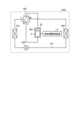
- FIG. 2 is a diagram showing an example of the configuration of the AC-DC converter 2 according to the first embodiment.
- the AC-DC converter 2 according to the first embodiment mainly comprises a control unit 6, a rectifier circuit 20, a reactor 212, and a capacitor 216.
- the AC-DC converter 2 also comprises a current detector 211 and voltage detectors 217a and 217b as means for detecting voltage or current.
- the voltage detector 217b when the voltage detectors 217a and 217b are to be distinguished from each other without reference numbers, the voltage detector 217b will be referred to as the "first voltage detector” and the voltage detector 217a will be referred to as the "second voltage detector.”
- the control unit 6 receives the detection values of the voltage detection units 217a, 217b and the current detection unit 211. Based on each detection value, the control unit 6 generates a switching signal for controlling the on/off of the switching element 215.
- An example of the switching element 215 is an IGBT (Insulated Gate Bipolar Transistor) as shown in the figure, but is not limited to an IGBT. Any element capable of switching operation may be used as the switching element 215.
- Another example of the switching element 215 is a MOSFET (Metal-Oxide-Semiconductor Field-Effect Transistor).
- the AC-DC converter 2 shown in FIG. 2 is configured as a closed loop using the detection values of the voltage detectors 217a, 217b and the current detector 211, but may be configured as an open loop using target values, estimated values, etc. If the AC-DC converter 2 is configured as an open loop, it is also possible to control the switching element 215 without using the detection values of the voltage detectors 217a, 217b and the current detector 211.
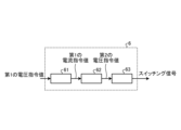
- FIG. 3 is a block diagram showing an example configuration of the control unit 6 according to the first embodiment.
- the control unit 6 includes a voltage control unit 61, a current control unit 62, and a switching signal generation unit 63.
- the voltage control unit 61 generates a first current command value using a first voltage command value.
- the current control unit 62 generates a second voltage command value using the first current command value.
- the switching signal generation unit 63 generates a switching signal using the second voltage command value.
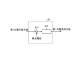
- FIG. 4 is a block diagram showing an example of the configuration of the voltage control unit 61 according to the first embodiment.
- the voltage control unit 61 includes a voltage controller 611 and a subtractor 612.
- the voltage control unit 61 generates a first current command value using a first voltage command value that is a command value for the bus voltage.
- the subtractor 612 generates a voltage deviation that is the difference between the first voltage command value and the detected voltage detected by the voltage detection unit 217b.
- the voltage controller 611 generates the first current command value using the voltage deviation output from the subtractor 612.
- the voltage controller 611 can be configured, for example, by a PI controller.
- the transfer function G AVR(s) can be expressed by the following equation (1).
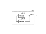
- Fig. 6 is a block diagram showing a configuration example in which the current controller 621 shown in Fig. 5 is configured as a PS controller.
- the current controller 621 is a controller configured to connect a P controller 621A and an S controller 621B in parallel, and add and output the outputs of the P controller 621A and the S controller 621B by an adder 621C.
- the S controller 621B is a controller with improved tracking performance for a sine wave input of angular frequency ⁇ n . The reason why the tracking performance of the S controller 621B is improved for an input pulsating with angular frequency ⁇ n can be explained by the internal model principle.
- the transfer function G ACR(s) can be expressed by the following equation (2).
- ACR in the transfer function G ACR(s) is an abbreviation for "Automatic Current Regulator.”
- K pACR is a proportional gain
- K sACR is an S control gain
- ⁇ n is an angular frequency
- s is a Laplace operator.
- the proportional gain K pACR , the S control gain K sACR , and the angular frequency ⁇ n can be arbitrarily determined.
- FIG. 7 is a block diagram showing a configuration example in which a target value filter 624 is introduced into the current control unit 62 shown in FIG. 5.
- FIG. 8 is a block diagram used to explain the transfer function of the current control system 7 in the AC/DC converter 2 including the current control unit 62 shown in FIG. 7.
- the closed loop transfer function G close(s) in the current control system 7 in FIG. 8 can be expressed by the following equation (3).
- Gc is the transfer function of an arbitrary controller 72
- Gp is the transfer function of an arbitrary controlled plant 73.
- G X is an arbitrary transfer function.
- the transfer function G X may be the value of the zeroth power term of the Laplace operator s in the denominator polynomial of the transfer function G' close(s) , or may have an arbitrary zero point.
- the controller response can be adjusted.
- a PI controller may be used as a controller that obtains the same effect as the target value filter 74.
- the carrier signal generator 631 generates a carrier signal used to generate a switching signal and outputs it to the comparator 632.
- the carrier signal is a bipolar or unipolar signal having a triangular waveform that operates at any frequency.
- the comparator 632 generates a switching signal based on the output of the standardizer 630 and the output of the carrier signal generator 631. In more detail, the comparator 632 compares the output value of the standardizer 630 with the output value of the carrier signal generator 631, and if the output value of the standardizer 630 is greater than the output value of the carrier signal generator 631, it outputs a signal to turn on the switching element 215.
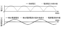
- the fundamental wave component of the detected power supply current is almost equal to the power supply current command value.
- the fundamental wave of the detected power supply current can track the power supply current command value even under conditions where the bus voltage is equal to or below the peak value of the absolute value of the power supply voltage.
- Figure 11 shows the results for operating conditions where the bus voltage is equal to or below the peak value of the absolute value of the power supply voltage, but it goes without saying that the fundamental wave of the detected power supply current will track the power supply current command value even under operating conditions where the bus voltage exceeds the peak value of the absolute value of the power supply voltage.
- variable carrier frequency control when variable carrier frequency control is used, the carrier frequency components can be dispersed, making it possible to reduce switching loss and switching noise while also reducing the effort required to make the harmonic components of the power supply current comply with harmonic standard values.
- the carrier signal generator 631 increases the count value by one for each clock up to the maximum carrier count crpk, which is set according to the carrier frequency. After the count value reaches the maximum carrier count crpk, the carrier signal generator 631 decreases the count value by one for each clock. In this way, the carrier signal generator 631 generates a triangular wave carrier signal that operates at a desired frequency by increasing or decreasing the carrier count value by one while setting the maximum carrier count crpk.
- the maximum carrier count crpk is defined by the following equation (7).
- the inventors performed carrier frequency variable control while setting a lower limit value for the carrier frequency, and performed simulations using several frequency variable patterns to determine whether the harmonic components contained in the power supply current comply with the harmonic standard value for the power supply current. Based on the simulation results, the inventors found that there is a preferable lower limit value for the carrier frequency. This lower limit value is explained below.
- the first and second frequency variable patterns shown in Fig. 13 and Fig. 14 are both patterns in which the carrier frequency is changed in the order of first frequency f cr1 ⁇ second frequency f cr2 ⁇ third frequency f cr3 ⁇ first frequency f cr1 , between 0 and 0.01 [s], which is a half cycle of the power supply voltage.
- the difference between the two is that the first frequency f cr1 , which is the lower limit, is set to 150 [Hz] in the first frequency variable pattern shown in Fig. 13, whereas it is set to 140 "Hz" in the second frequency variable pattern shown in Fig. 14.
- the second frequency f cr2 and the third frequency f cr3 are the same value in both cases.
- the inventors of the present application conducted a simulation in which the second frequency f cr2 and the third frequency f cr3 were common and the first frequency f cr1 , which is the lower limit of the carrier frequency, was changed, and found that the operation of the control unit 6 did not become unstable if the lower limit of the carrier frequency was set to 150 [Hz] as shown in Fig. 13. On the other hand, when the lower limit of the carrier frequency was set to less than 150 [Hz] as shown in Fig. 14, some of the simulation results showed that the operation of the control unit 6 became unstable.
- FIG. 15 is a diagram showing an example of current harmonic characteristics when a PI controller is applied to the current control unit 62 shown in FIG. 7.
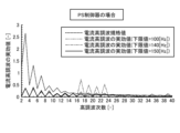
- FIG. 16 is a diagram showing an example of current harmonic characteristics when a PS controller is applied to the current control unit 62 shown in FIG. 7. In both diagrams, the horizontal axis shows the harmonic order, and the vertical axis shows the effective value of the current harmonic.
- the lower limit may be set to 150 Hz or more.
- the operation of the controller follows a sine wave command, so it is possible to make the lower limit even smaller than in the case of a PI controller.
- Embodiment 2 In the second embodiment, a different example of the AC-DC converter 2 including the control unit 6 described in the first embodiment will be described. Components having the same or equivalent functions as those of the AC-DC converter 2 described in the first embodiment will be denoted by the same reference numerals, and overlapping descriptions will be omitted.
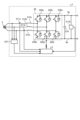
- FIG. 17 is a diagram showing an example of the configuration of an AC-DC converter 2 according to embodiment 2.
- the rectifier circuit 20 is composed of a single-phase H-bridge cell having four switching elements 220a, 220b, 220c, and 220d. Note that the configuration and operation of the rectifier circuit 20 shown in FIG. 17 are publicly known, and further description will be omitted here.
- the control unit 6 generates switching signals for the four switching elements 220a, 220b, 220c, and 220d using the control method described in embodiment 1 to drive them. This allows the AC-DC converter 2 shown in FIG. 17 to achieve the same effects as in embodiment 1.
- the switching elements 220a, 220b, 220c, and 220d are shown as IGBTs, but any elements capable of switching operation may be used.
- the AC-DC converter 2 shown in FIG. 17 is configured as a closed loop, but it may also be configured as an open loop. When the AC-DC converter 2 is configured as an open loop, the detection values of the voltage detectors 217a and 217b and the current detector 211 do not need to be used.
- Embodiment 3 a different example of the AC-DC converter 2 including the control unit 6 described in the first embodiment will be described. Components having the same or equivalent functions as those of the AC-DC converter 2 described in the first embodiment will be denoted by the same reference numerals, and description of the overlapping contents will be omitted.
- FIG. 18 is a diagram showing an example of the configuration of an AC-DC converter 2 according to the third embodiment.
- the rectifier circuit 20 is composed of a single-phase H-bridge cell including two diodes 218a, 218b and two switching elements 220c, 220d.
- one leg is composed of a series circuit of diodes 218a, 218b, and the other leg is composed of a series circuit of switching elements 220c, 220d.
- the configuration and operation of the rectifier circuit 20 shown in FIG. 18 are publicly known, and further description will be omitted here.
- the control unit 6 generates switching signals for the two switching elements 220c and 220d using the control method described in embodiment 1 to drive them. This allows the AC-DC converter 2 shown in FIG. 18 to achieve the same effects as in embodiment 1.
- the switching elements 220c and 220d are shown as IGBTs, but any elements capable of switching operation may be used.
- the AC-DC converter 2 shown in FIG. 18 is configured as a closed loop, but it may also be configured as an open loop. When the AC-DC converter 2 is configured as an open loop, it is not necessary to use the detection values of the voltage detectors 217a and 217b and the current detector 211.
- Embodiment 4 a different example of the AC-DC converter 2 including the control unit 6 described in the first embodiment will be described. Components having the same or equivalent functions as those of the AC-DC converter 2 described in the first embodiment will be denoted by the same reference numerals, and description of the overlapping contents will be omitted.
- FIG. 19 is a diagram showing an example of the configuration of an AC-DC converter 2 according to embodiment 4.
- the rectifier circuit 20 is composed of a single-phase H-bridge cell including two diodes 218a, 218c and two switching elements 220b, 220d.
- the diodes 218a, 218c are arranged in the upper arms of the two legs, and the switching elements 220b, 220d are arranged in the lower arms of the two legs.
- the configuration and operation of the rectifier circuit 20 shown in FIG. 19 are publicly known, and further description will be omitted here.
- the control unit 6 generates switching signals for the two switching elements 220b and 220d using the control method described in embodiment 1 to drive them. This allows the AC-DC converter 2 shown in FIG. 19 to achieve the same effects as in embodiment 1.
- the switching elements 220b and 220d are shown as IGBTs, but any elements capable of switching operation may be used.
- the AC-DC converter 2 shown in FIG. 19 is configured as a closed loop, but it may also be configured as an open loop. When the AC-DC converter 2 is configured as an open loop, it is not necessary to use the detection values of the voltage detectors 217a and 217b and the current detector 211.
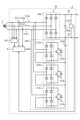
- FIG. 20 is a diagram showing an example of the configuration of an AC-DC converter 2 according to embodiment 5.
- the rectifier circuit 20 is composed of a single-phase H-bridge cell including two diodes 218a, 218b, four switching elements 220a, 220b, 220c, and 220d, a capacitor 216b, and a voltage detector 217c.
- the voltage detector 217c may be provided outside the rectifier circuit 20.
- one leg is composed of a series circuit of diodes 218a and 218b, and the other leg is composed of a series circuit of switching elements 220a, 220b, 220c, and 220d.
- the capacitor 216b is connected between the connection point of the switching elements 220a and 220b and the connection point of the switching elements 220c and 220d.
- the voltage detection unit 217c detects the voltage of the capacitor 216b and outputs the detection value to the control unit 6.
- the control unit 6 generates a switching signal for controlling the switching elements 220a, 220b, 220c, and 220d based on the detection values of the voltage detection units 217a, 217b, and 217c and the current detection unit 211.
- the configuration and operation of the rectifier circuit 20 shown in FIG. 20 are publicly known, and further description is omitted here.
- the control unit 6 generates switching signals for the four switching elements 220a, 220b, 220c, and 220d using the control method described in embodiment 1 to drive them. This allows the AC-DC converter 2 shown in FIG. 20 to achieve the same effects as in embodiment 1.
- the switching elements 220a, 220b, 220c, and 220d are shown as IGBTs, but any elements capable of switching operation may be used.
- the AC-DC converter 2 shown in FIG. 20 is configured as a closed loop, but it may also be configured as an open loop. When the AC-DC converter 2 is configured as an open loop, the detection values of the voltage detectors 217a, 217b, and 217c and the current detector 211 do not need to be used.
- Embodiment 6 a different example of the AC-DC converter 2 including the control unit 6 described in the first embodiment will be described. Components having the same or equivalent functions as those of the AC-DC converter 2 described in the first embodiment will be denoted by the same reference numerals, and description of the overlapping contents will be omitted.
- FIG. 21 is a diagram showing an example of the configuration of an AC-DC converter 2 according to embodiment 6.
- the rectifier circuit 20 is composed of a single-phase H-bridge cell 221 and a switching cell 222.
- the single-phase H-bridge cell 221 includes two diodes 218a and 218c and two switching elements 220b and 220d.
- the switching cell 222 includes four switching elements 220e, 220f, 220g, and 220h, a capacitor 216c, and a voltage detection unit 217c.
- the voltage detection unit 217c may be provided outside the switching cell 222.
- diodes 218a and 218c are arranged in the upper arms of the two legs, and switching elements 220b and 220d are arranged in the lower arms of the two legs.
- switching cell 222 shown in FIG. 21 four switching elements 220e, 220f, 220g, and 220h are bridge-connected.
- the capacitor 216c is connected in parallel to the first leg consisting of the switching elements 220e and 220f and the second leg consisting of the switching elements 220g and 220h.
- switching elements 220b, 220d, 220e, 220f, 220g, and 220h are shown as IGBTs, but any elements capable of switching may be used.
- the AC-DC converter 2 shown in FIG. 21 is configured as a closed loop, it may also be configured as an open loop. When the AC-DC converter 2 is configured as an open loop, the detection values of voltage detectors 217a, 217b, and 217c and current detector 211 do not need to be used.
- the control unit 6 generates switching signals for the two switching elements 220a and 220b using the control method described in embodiment 1 to drive them. This allows the AC-DC converter 2 shown in FIG. 22 to achieve the same effects as in embodiment 1.
- the switching elements 215a, 215b, and 215c are shown as IGBTs, but any elements capable of switching operation may be used.
- the AC-DC converter 2 shown in FIG. 24 is configured as a closed loop, but it may also be configured as an open loop. When the AC-DC converter 2 is configured as an open loop, the detection values of the voltage detectors 227 and 217b and the current detectors 211a and 211b do not need to be used.
- the control according to the ninth embodiment may be performed on ⁇ coordinates or on three-phase coordinates.
- FIG. 25 is a diagram showing an example of the configuration of an AC-DC converter 2 according to embodiment 10.
- the capacitor 216d is removed from the configuration of the AC-DC converter 2 of FIG. 24. The rest is the same as or equivalent to FIG. 24.
- the control unit 6 generates switching signals for the three switching elements 215a, 215b, and 215c using the control method described in embodiment 1 to drive them. This allows the AC-DC converter 2 shown in FIG. 25 to achieve the same effects as in embodiment 1.
- the switching elements 215a, 215b, and 215c are shown as IGBTs, but any elements capable of switching operation may be used.
- the AC-DC converter 2 shown in FIG. 25 is configured as a closed loop, but it may also be configured as an open loop. When the AC-DC converter 2 is configured as an open loop, the detection values of the voltage detectors 227 and 217b and the current detectors 211a and 211b do not need to be used.
- the control according to the tenth embodiment may be performed on ⁇ coordinates or on three-phase coordinates.
- the control unit 6 generates a switching signal for the switching element 215 using the control method described in the first embodiment to drive the switching element 215.
- the AC-DC converter 2 shown in FIG. 27 can achieve the same effect as in the first embodiment.
- Embodiment 13 In the thirteenth embodiment, a different example of the AC-DC converter 2 including the control unit 6 described in the first embodiment will be described. Components having the same or equivalent functions as those of the AC-DC converter 2 described in the first and eighth embodiments will be denoted by the same reference numerals, and description of the overlapping contents will be omitted.
- FIG. 28 is a diagram showing an example of the configuration of an AC-DC converter 2 according to embodiment 13.
- the rectifier circuit 20 is composed of a three-phase diode bridge cell 228 and a three-phase bidirectional switching cell 231.
- the three-phase bidirectional switching cell 231 has six switching elements 231a, 231b, 231c, 231d, 231e, and 231f.
- the capacitor 216 in FIG. 23 is replaced with two capacitors 216a and 216b connected in series.
- the series-connected capacitors 216a and 216b are connected between the DC buses 9a and 9b.
- the switching elements 231a and 231b, the switching elements 231c and 231d, and the switching elements 231e and 231f are connected in series in pairs. Each series-connected pair is arranged for each phase between the three-phase diode bridge cell 228 and the connection point of the capacitors 216a and 216b. Note that the configuration and operation of the rectifier circuit 20 shown in FIG. 28 are publicly known, and further description will be omitted here.
- the control unit 6 generates switching signals for the six switching elements 231a, 231b, 231c, 231d, 231e, and 231f using the control method described in embodiment 1 to drive them. This allows the AC/DC converter 2 shown in FIG. 28 to achieve the same effects as in embodiment 1.
- the switching elements 231a, 231b, 231c, 231d, 231e, and 231f are shown as IGBTs, but any elements capable of switching operation may be used.
- the AC-DC converter 2 shown in FIG. 28 is configured as a closed loop, but it may also be configured as an open loop. When the AC-DC converter 2 is configured as an open loop, the detection values of the voltage detectors 227 and 217b and the current detectors 211a and 211b do not need to be used.
- the control according to the thirteenth embodiment may be performed on ⁇ coordinates or on three-phase coordinates.
- Embodiment 14 In the fourteenth embodiment, a different example of the AC-DC converter 2 including the control unit 6 described in the first embodiment will be described. Components having the same or equivalent functions as those of the AC-DC converter 2 described in the first embodiment will be denoted by the same reference numerals, and description of the overlapping contents will be omitted.
- FIG. 29 is a diagram showing an example of the configuration of an AC-DC converter 2 according to embodiment 14.
- the rectifier circuit 20 is composed of a single-phase diode bridge cell 213a and an interleave cell 219.
- the interleave cell 219 is a full PAM circuit configuration described in FIG. 12 with two sets of reactor 212, switching element 215, and diode 218.
- the interleave cell 219 includes reactors 2191a and 2191b, diodes 2192a and 2192b, and switching elements 2193a and 2193b.
- the configuration and operation of the rectifier circuit 20 shown in FIG. 29 are publicly known, and further description here is omitted.
- the control unit 6 generates switching signals for the two switching elements 2193a and 2193b using the control method described in embodiment 1 to drive them. This allows the AC-DC converter 2 shown in FIG. 29 to achieve the same effects as in embodiment 1.
- switching elements 2193a and 2193b are shown as IGBTs in FIG. 29, any elements capable of switching operation may be used.
- the AC-DC converter 2 shown in FIG. 29 is configured as a closed loop, it may also be configured as an open loop. When the AC-DC converter 2 is configured as an open loop, it is not necessary to use the detection values of the voltage detectors 217a and 217b and the current detector 211.
- FIG. 29 shows an example in which the interleaved cells 219 are configured in two stages, the interleaved cells 219 may also be configured in three or more stages.
- the rectifier circuits 20 shown in the first to fourteenth embodiments may also be configured in an interleaved configuration.
- the refrigeration cycle application device 900 includes a compressor 42 incorporating the motor 41 in the first embodiment, a four-way valve 902, an indoor heat exchanger 906, an expansion valve 908, and an outdoor heat exchanger 910 attached via refrigerant piping 912. Inside the compressor 42, there is provided a compression mechanism 904 that compresses the refrigerant, and a motor 41 that operates the compression mechanism 904.
- the refrigeration cycle application device 900 can perform heating or cooling operation by switching the four-way valve 902.
- the compression mechanism 904 is driven by a motor 41 that is variable speed controlled.
- the refrigerant is pressurized by the compression mechanism 904 and sent out, and returns to the compression mechanism 904 through the four-way valve 902, the indoor heat exchanger 906, the expansion valve 908, the outdoor heat exchanger 910, and the four-way valve 902.
- the refrigerant is pressurized by the compression mechanism 904 and sent out, and returns to the compression mechanism 904 through the four-way valve 902, the outdoor heat exchanger 910, the expansion valve 908, the indoor heat exchanger 906, and the four-way valve 902.
- the indoor heat exchanger 906 acts as a condenser to release heat, and the outdoor heat exchanger 910 acts as an evaporator to absorb heat.
- the outdoor heat exchanger 910 acts as a condenser to release heat, and the indoor heat exchanger 906 acts as an evaporator to absorb heat.
- the expansion valve 908 reduces the pressure of the refrigerant and causes it to expand.
- the refrigeration cycle application device 900 according to embodiment 15 has been described as including the rotating machine drive device 8 described in embodiment 1, but is not limited to this. It may also be provided with a rotating machine drive device 8 including the rectifier circuit 20 described in embodiments 2 to 14. Furthermore, the rotating machine drive device 8 may include a rectifier circuit other than the rectifier circuit 20 described in embodiments 1 to 14, as long as the control method of embodiment 1 can be applied.
Landscapes
- Engineering & Computer Science (AREA)
- Power Engineering (AREA)
- Rectifiers (AREA)
Priority Applications (2)
| Application Number | Priority Date | Filing Date | Title |
|---|---|---|---|
| JP2025566162A JPWO2025141866A1 (https=) | 2023-12-28 | 2023-12-28 | |
| PCT/JP2023/047277 WO2025141866A1 (ja) | 2023-12-28 | 2023-12-28 | 交流直流変換装置、回転機駆動装置及び冷凍サイクル適用機器 |
Applications Claiming Priority (1)
| Application Number | Priority Date | Filing Date | Title |
|---|---|---|---|
| PCT/JP2023/047277 WO2025141866A1 (ja) | 2023-12-28 | 2023-12-28 | 交流直流変換装置、回転機駆動装置及び冷凍サイクル適用機器 |
Publications (1)
| Publication Number | Publication Date |
|---|---|
| WO2025141866A1 true WO2025141866A1 (ja) | 2025-07-03 |
Family
ID=96217177
Family Applications (1)
| Application Number | Title | Priority Date | Filing Date |
|---|---|---|---|
| PCT/JP2023/047277 Pending WO2025141866A1 (ja) | 2023-12-28 | 2023-12-28 | 交流直流変換装置、回転機駆動装置及び冷凍サイクル適用機器 |
Country Status (2)
| Country | Link |
|---|---|
| JP (1) | JPWO2025141866A1 (https=) |
| WO (1) | WO2025141866A1 (https=) |
Citations (3)
| Publication number | Priority date | Publication date | Assignee | Title |
|---|---|---|---|---|
| JP2011125147A (ja) * | 2009-12-11 | 2011-06-23 | Hitachi Ltd | 電源回路及びそれを用いたモータ駆動装置並びに冷凍機器 |
| JP2016144323A (ja) * | 2015-02-03 | 2016-08-08 | ジョンソンコントロールズ ヒタチ エア コンディショニング テクノロジー(ホンコン)リミテッド | 直流電源装置およびこれを用いた空気調和機 |
| JP6151034B2 (ja) * | 2013-01-31 | 2017-06-21 | 三菱重工業株式会社 | コンバータ装置及び空気調和機 |
-
2023
- 2023-12-28 WO PCT/JP2023/047277 patent/WO2025141866A1/ja active Pending
- 2023-12-28 JP JP2025566162A patent/JPWO2025141866A1/ja active Pending
Patent Citations (3)
| Publication number | Priority date | Publication date | Assignee | Title |
|---|---|---|---|---|
| JP2011125147A (ja) * | 2009-12-11 | 2011-06-23 | Hitachi Ltd | 電源回路及びそれを用いたモータ駆動装置並びに冷凍機器 |
| JP6151034B2 (ja) * | 2013-01-31 | 2017-06-21 | 三菱重工業株式会社 | コンバータ装置及び空気調和機 |
| JP2016144323A (ja) * | 2015-02-03 | 2016-08-08 | ジョンソンコントロールズ ヒタチ エア コンディショニング テクノロジー(ホンコン)リミテッド | 直流電源装置およびこれを用いた空気調和機 |
Also Published As
| Publication number | Publication date |
|---|---|
| JPWO2025141866A1 (https=) | 2025-07-03 |
Similar Documents
| Publication | Publication Date | Title |
|---|---|---|
| EP2309635B1 (en) | Ac-dc converter, ac-dc converter control method, motor driving device, compressor driving device, air conditioner, and heat pump-type hot-water supply device | |
| JP3422218B2 (ja) | コンバータ | |
| CN103098362B (zh) | 电力变换装置、电动机驱动设备、制冷空调设备 | |
| CN102005949A (zh) | 变换装置、电动机驱动用模块、冷冻装置及高次谐波降低装置 | |
| WO2022149206A1 (ja) | 電力変換装置、モータ駆動装置及び冷凍サイクル適用機器 | |
| WO2022091186A1 (ja) | 電力変換装置、モータ駆動装置および冷凍サイクル適用機器 | |
| JP7507894B2 (ja) | 電力変換装置、モータ駆動装置及び冷凍サイクル適用機器 | |
| KR102014257B1 (ko) | 전력변환장치 및 이를 포함하는 공기조화기 | |
| WO2025141866A1 (ja) | 交流直流変換装置、回転機駆動装置及び冷凍サイクル適用機器 | |
| CN113678361B (zh) | 空调装置 | |
| JP7625158B1 (ja) | 交流直流変換装置、回転機駆動装置及び冷凍サイクル適用機器 | |
| WO2025141865A1 (ja) | 交流直流変換装置、回転機駆動装置及び冷凍サイクル適用機器 | |
| KR101905480B1 (ko) | 모터 구동장치 및 이를 구비하는 공기조화기 | |
| JPWO2018109805A1 (ja) | 高調波電流補償装置および空気調和システム | |
| JP7603906B1 (ja) | 交流直流変換装置、回転機駆動装置及び冷凍サイクル適用機器 | |
| KR101624048B1 (ko) | 전력 변환 장치 및 공기 조화기 | |
| JP7603907B1 (ja) | 交流直流変換装置、回転機駆動装置及び冷凍サイクル適用機器 | |
| WO2025141871A1 (ja) | 交流直流変換装置、回転機駆動装置及び冷凍サイクル適用機器 | |
| WO2025141870A1 (ja) | 交流直流変換装置、回転機駆動装置及び冷凍サイクル適用機器 | |
| WO2025141867A1 (ja) | 交流直流変換装置、回転機駆動装置及び冷凍サイクル適用機器 | |
| WO2025141868A1 (ja) | 交流直流変換装置、回転機駆動装置及び冷凍サイクル適用機器 | |
| KR101049930B1 (ko) | 공기조화기의 전동기 구동장치 | |
| WO2022149213A1 (ja) | 電力変換装置、モータ駆動装置および冷凍サイクル適用機器 | |
| WO2025141872A1 (ja) | 交流直流変換装置、回転機駆動装置及び冷凍サイクル適用機器 | |
| WO2025004328A1 (ja) | 電力変換装置および冷凍サイクル適用機器 |
Legal Events
| Date | Code | Title | Description |
|---|---|---|---|
| 121 | Ep: the epo has been informed by wipo that ep was designated in this application |
Ref document number: 23963211 Country of ref document: EP Kind code of ref document: A1 |
|
| ENP | Entry into the national phase |
Ref document number: 2025566162 Country of ref document: JP Kind code of ref document: A |
|
| WWE | Wipo information: entry into national phase |
Ref document number: 2025566162 Country of ref document: JP |