WO2025134641A1 - 圧電センサ - Google Patents
圧電センサ Download PDFInfo
- Publication number
- WO2025134641A1 WO2025134641A1 PCT/JP2024/040930 JP2024040930W WO2025134641A1 WO 2025134641 A1 WO2025134641 A1 WO 2025134641A1 JP 2024040930 W JP2024040930 W JP 2024040930W WO 2025134641 A1 WO2025134641 A1 WO 2025134641A1
- Authority
- WO
- WIPO (PCT)
- Prior art keywords
- electrode
- piezoelectric sensor
- piezoelectric
- film
- main surface
- Prior art date
- Legal status (The legal status is an assumption and is not a legal conclusion. Google has not performed a legal analysis and makes no representation as to the accuracy of the status listed.)
- Pending
Links
Images







Classifications
-
- G—PHYSICS
- G01—MEASURING; TESTING
- G01L—MEASURING FORCE, STRESS, TORQUE, WORK, MECHANICAL POWER, MECHANICAL EFFICIENCY, OR FLUID PRESSURE
- G01L1/00—Measuring force or stress, in general
- G01L1/16—Measuring force or stress, in general using properties of piezoelectric devices
-
- H—ELECTRICITY
- H10—SEMICONDUCTOR DEVICES; ELECTRIC SOLID-STATE DEVICES NOT OTHERWISE PROVIDED FOR
- H10N—ELECTRIC SOLID-STATE DEVICES NOT OTHERWISE PROVIDED FOR
- H10N30/00—Piezoelectric or electrostrictive devices
- H10N30/01—Manufacture or treatment
- H10N30/06—Forming electrodes or interconnections, e.g. leads or terminals
-
- H—ELECTRICITY
- H10—SEMICONDUCTOR DEVICES; ELECTRIC SOLID-STATE DEVICES NOT OTHERWISE PROVIDED FOR
- H10N—ELECTRIC SOLID-STATE DEVICES NOT OTHERWISE PROVIDED FOR
- H10N30/00—Piezoelectric or electrostrictive devices
- H10N30/30—Piezoelectric or electrostrictive devices with mechanical input and electrical output, e.g. functioning as generators or sensors
-
- H—ELECTRICITY
- H10—SEMICONDUCTOR DEVICES; ELECTRIC SOLID-STATE DEVICES NOT OTHERWISE PROVIDED FOR
- H10N—ELECTRIC SOLID-STATE DEVICES NOT OTHERWISE PROVIDED FOR
- H10N30/00—Piezoelectric or electrostrictive devices
- H10N30/80—Constructional details
- H10N30/85—Piezoelectric or electrostrictive active materials
- H10N30/857—Macromolecular compositions
-
- H—ELECTRICITY
- H10—SEMICONDUCTOR DEVICES; ELECTRIC SOLID-STATE DEVICES NOT OTHERWISE PROVIDED FOR
- H10N—ELECTRIC SOLID-STATE DEVICES NOT OTHERWISE PROVIDED FOR
- H10N30/00—Piezoelectric or electrostrictive devices
- H10N30/80—Constructional details
- H10N30/87—Electrodes or interconnections, e.g. leads or terminals
Definitions
- the present invention relates to a piezoelectric sensor that detects deformation.
- a piezoelectric sensor described in Patent Document 1 is known as an invention related to a conventional piezoelectric sensor.
- the piezoelectric sensor described in Patent Document 1 is disposed on the inner wall surface of a cylindrical housing, and is pressed from the outer peripheral side surface (pressing surface) of the housing to detect deformation due to the pressure.
- the piezoelectric sensor described in Patent Document 1 includes an insulating base material having two main surfaces facing each other, a first electrode, a second electrode, a piezoelectric film having an upper surface and a lower surface, and a conductive thin film member.
- the first electrode and the second electrode are formed on both main surfaces of the insulating base material, respectively.
- the second electrode is attached to the inner wall surface of the housing with an adhesive or the like.
- the lower surface of the piezoelectric film is attached to the upper surface of the first electrode.
- a conductive thin film member is attached to the upper surface of the piezoelectric film.
- the object of the present invention is to provide a piezoelectric sensor that can suppress changes in sensitivity to deformation caused by variations in the thickness of the insulating substrate.
- a piezoelectric sensor includes: an insulating substrate having a first upper principal surface and a first lower principal surface; a first electrode formed on the first upper main surface; and a plurality of electrodes formed on at least the first upper main surface; a piezoelectric film having a second upper principal surface and a second lower principal surface, the second lower principal surface being disposed opposite the first electrode; Equipped with In a plan view, in a region where the insulating base material and the piezoelectric film overlap, the multiple electrodes do not overlap one another in a plan view.
- the piezoelectric sensor When the piezoelectric sensor is deformed by pressure in the normal direction of the insulating substrate, the upper principal surface of the piezoelectric sensor contracts and the lower principal surface expands.
- the position of the insulating substrate in a cross-sectional view is close to the center position of the thickness of the piezoelectric sensor. Therefore, in the structure of the piezoelectric sensor described in Patent Document 1, the neutral plane of stress (the part that does not expand or contract) of the piezoelectric sensor is located in the insulating substrate. Therefore, in the structure of the piezoelectric sensor described in Patent Document 1, the sensitivity of the piezoelectric sensor changes significantly due to the variation in the thickness of the insulating substrate.
- the piezoelectric sensor according to one embodiment of the present invention in the region where the insulating substrate and the piezoelectric film overlap in a plan view, the multiple electrodes do not overlap each other in a plan view, so that when the piezoelectric sensor is pressed, the neutral plane of stress is not located in the insulating substrate.
- the piezoelectric sensor when the piezoelectric sensor is pressed, it is possible to prevent the insulating substrate from being located in the range from the piezoelectric film to the neutral plane of stress.
- the present invention makes it possible to suppress changes in sensitivity to deformation caused by variations in the thickness of the insulating substrate.
- FIG. 1 is a perspective view of a piezoelectric sensor 1.
- FIG. 2 is an exploded perspective view of the piezoelectric sensor 1.
- FIG. 3 is a plan view of the first electrode 3, the second electrode 4, and the third electrode 5 as viewed from below.
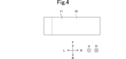
- FIG. 4 is a plan view of the shielding tape 11 as viewed downward.
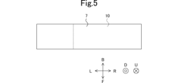
- FIG. 5 is a plan view of the shielding film 7 as viewed from above.
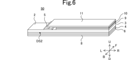
- FIG. 6 is a perspective view of a piezoelectric sensor 50 according to a comparative example.
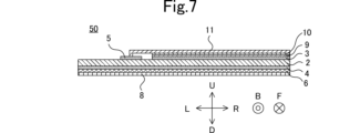
- FIG. 7 is a cross-sectional view of the piezoelectric sensor 50.
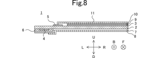
- FIG. 8 is a cross-sectional view of the piezoelectric sensor 1.
- FIG. 1 is a perspective view of a piezoelectric sensor 1.
- FIG. 2 is an exploded perspective view of the piezoelectric sensor 1.
- FIG. 3 is a plan view of the first electrode 3, the second electrode 4, and the third electrode 5 as viewed from below.
- FIG. 4 is
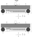
- FIG. 9 is a schematic cross-sectional view of the piezoelectric sensor 50 and the piezoelectric sensor 1 in the first simulation.
- FIG. 10 is a diagram showing the amount of strain of each member in a first simulation of the piezoelectric sensor 50.
- FIG. 11 is a diagram showing the amount of strain of each member in the first simulation of the piezoelectric sensor 1.
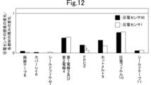
- FIG. 12 is a diagram showing changes in sensitivity of the piezoelectric sensor 50 and the piezoelectric sensor 1 with respect to changes in thickness of each member of the piezoelectric sensor 50 and the piezoelectric sensor 1 in the first simulation.
- FIG. 13 is an example of a diagram showing the amount of strain of each member in the second simulation of the piezoelectric sensor 1. In FIG. FIG. FIG.
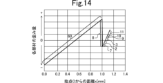
- FIG. 14 is an example of a diagram showing the amount of strain of each member in the second simulation of the piezoelectric sensor 1.
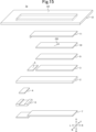
- FIG. 15 is an exploded perspective view of the piezoelectric sensor 1a.
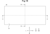
- FIG. 16 is a plan view of the piezoelectric sensor 1a.
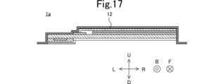
- FIG. 17 is a cross-sectional view taken along line AA in FIG.
- FIG. 18 is a cross-sectional view taken along line BB in FIG.
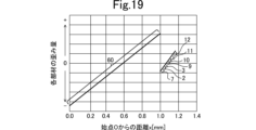
- FIG. 19 is a diagram showing the amount of strain of each member in the third simulation of the piezoelectric sensor 1a.
- FIG. 20 is a diagram showing the amount of distortion of each member in a simulation of the piezoelectric sensor 1 when the pressed portion overlaps with the second electrode 4 as viewed in the vertical direction.
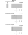
- FIG. 21 is a plan view showing the area where the second electrode 4 and the piezoelectric film 10 overlap each other, as viewed from above.
- Fig. 1 is a perspective view of the piezoelectric sensor 1.
- Fig. 2 is an exploded perspective view of the piezoelectric sensor 1.
- Fig. 3 is a plan view of the first electrode 3, the second electrode 4, and the third electrode 5 as viewed from below.
- Fig. 4 is a plan view of the shielding tape 11 as viewed from below.
- Fig. 5 is a plan view of the shielding film 7 as viewed from above.
- directions are defined as follows. As shown in FIG. 1, the direction in which the long side of the upper main surface US2 of the FPC2 extends is defined as the left-right direction. The direction in which the short side of the upper main surface US2 of the FPC2 extends is defined as the front-rear direction. The direction in which the FPC2 and the piezoelectric film 10 are arranged is defined as the up-down direction. The left-right direction, front-rear direction, and up-down direction are mutually orthogonal. Viewing in the upward or downward direction corresponds to the "planar view" according to the present invention.
- left-right direction, front-rear direction, and up-down direction in this specification are directions defined for the convenience of explanation, and do not have to match the left-right direction, front-rear direction, and up-down direction when the piezoelectric sensor 1 is in use.
- the left direction and the right direction may be interchanged, the front direction and the rear direction may be interchanged, and the upward direction and the downward direction may be interchanged.
- the piezoelectric sensor 1 detects the deformation of the object to be measured.
- the piezoelectric sensor 1 is also highly flexible and can deform flexibly. This allows the piezoelectric sensor 1 to be attached to the object to be measured even if the object to be measured has unevenness.
- the piezoelectric sensor 1 includes an FPC 2, a first electrode 3, a second electrode 4, a third electrode 5, a coverlay 6, a shielding film 7, a double-sided tape 8, a hot melt 9, a piezoelectric film 10, and a shielding tape 11.
- the piezoelectric sensor 1 is attached to the object to be measured so that the piezoelectric film 10 is positioned directly below the pressing point of the object to be measured.
- the FPC 2 overlaps the first electrode 3, the second electrode 4, the third electrode 5, the coverlay 6, the shielding film 7, the double-sided tape 8, the hot melt 9, the piezoelectric film 10, and the shielding tape 11.
- the third electrode 5, coverlay 6, shielding film 7, double-sided tape 8, hot melt 9, and shielding tape 11 are not essential components.
- the FPC 2, shielding film 7, double-sided tape 8, hot melt 9, and shielding tape 11 correspond to the "insulating substrate”, "second conductive thin film member”, “third adhesive member”, “first adhesive member”, and “first conductive thin film member” in the present invention, respectively.
- the first electrode 3, second electrode 4, and third electrode 5 correspond to the "multiple electrodes" in the present invention.
- the FPC2 is a flexible insulating substrate.
- the material of the FPC2 is, for example, polyimide, PET (Poly Ethylene Terephthalate), or liquid crystal polymer.
- the FPC2 has an upper main surface US2 and a lower main surface DS2 arranged in this order in a downward direction.
- the upper main surface US2 and the lower main surface DS2 each have a rectangular shape with two long sides extending in the left-right direction and two short sides extending in the front-rear direction.
- the upper main surface US2 and the lower main surface DS2 correspond to the "first upper main surface” and the "first lower main surface” of the present invention, respectively.
- the shape and arrangement of the insulating substrate of the present invention are not limited to the shape and arrangement of the FPC2.
- the first electrode 3 is formed on the upper main surface US2 of the FPC 2.
- the upper and lower surfaces of the first electrode 3 each have a rectangular shape with two long sides extending in the left-right direction and two short sides extending in the front-rear direction.
- the first electrode 3 functions as a signal electrode for outputting the potential difference generated by the piezoelectric film 10 as an electric charge. Note that the shape and arrangement of the first electrode according to the present invention are not limited to the shape and arrangement of the first electrode 3.
- the second electrode 4 is formed on the lower main surface DS2 of the FPC 2.
- the upper and lower surfaces of the second electrode 4 each have a rectangular shape with two short sides extending in the left-right direction and two long sides extending in the front-rear direction.
- the second electrode 4 is connected to a ground potential. This allows the second electrode 4 to function as a shield electrode. Note that the shape and arrangement of the second electrode according to the present invention are not limited to the shape and arrangement of the second electrode 4.
- the second electrode 4 is not an essential component of the piezoelectric sensor according to the present invention.
- the multiple electrodes according to the present invention do not have to be formed on the lower main surface DS2 of the FPC 2, and may be formed only on the upper main surface US2 of the FPC 2.
- the third electrode 5 is formed on the upper main surface US2 of the FPC 2. That is, in this embodiment, the first electrode 3, the second electrode 4, and the third electrode 5 are formed on the upper main surface US2 and the lower main surface DS2 of the FPC 2.
- the upper and lower surfaces of the third electrode 5 each have a rectangular shape having two short sides extending in the left-right direction and two long sides extending in the front-rear direction.
- the third electrode 5 is disposed to the left of the first electrode 3.
- the third electrode 5 is connected to the ground potential.
- the third electrode 5 functions as a shield electrode.
- the shape and arrangement of the third electrode according to the present invention are not limited to the shape and arrangement of the third electrode 5.
- the third electrode 5 is not an essential component of the piezoelectric sensor according to the present invention.
- the coverlay 6 is flexible and insulating.
- the coverlay 6 is formed on the lower main surface DS2 of the FPC 2 so as to cover the second electrode 4. In this way, the coverlay 6 protects the second electrode 4.
- the material of the coverlay 6 is, for example, polyimide. Note that the shape and arrangement of the coverlay are not limited to those of the coverlay 6.
- the shielding film 7 is flexible and conductive.
- the shielding film 7 is flat.
- the shielding film 7 has an upper main surface US7 and a lower main surface DS7 arranged in this order along the downward direction.
- the upper main surface US7 is arranged to face the lower main surface DS2 of the FPC 2.
- the shielding film 7 is partially bent to cover the lower main surface DS2 of the FPC 2 and the coverlay 6.
- the shielding film 7 is connected to a ground potential.
- the connection of the shielding film 7 to a ground potential can be achieved, for example, by providing an opening in the coverlay 6 and connecting the shielding film 7 to the second electrode 4. This allows the shielding film 7 to function as a shielding conductor.
- the upper main surface US7 and the lower main surface DS7 correspond to the "fourth upper main surface” and the “fourth lower main surface” of the present invention, respectively.
- the shape and arrangement of the second conductive thin film member of the present invention are not limited to the shape and arrangement of the shielding film 7.
- the double-sided tape 8 is flexible.
- the double-sided tape 8 is in the form of a flat film.
- the upper and lower surfaces of the double-sided tape 8 are adhesive.
- the double-sided tape 8 is provided on the lower main surface DS7 of the shielding film 7.
- the upper surface of the double-sided tape 8 is partially bent so that it adheres to the lower main surface DS7 of the shielding film 7.
- the lower surface of the double-sided tape 8 is brought into close contact with the object to be measured, thereby attaching the piezoelectric sensor 1 to the object to be measured.
- the shape and arrangement of the third adhesive member according to the present invention are not limited to the shape and arrangement of the double-sided tape 8.
- the piezoelectric film 10 is flexible.
- the piezoelectric film 10 is flat.
- the piezoelectric film 10 covers the upper surface of the first electrode 3.
- the piezoelectric film 10 has an upper principal surface US10 and a lower principal surface DS10 arranged in this order along the downward direction.
- the lower principal surface DS10 is arranged so as to face the first electrode 3.
- the upper principal surface US10 and the lower principal surface DS10 each have a rectangular shape having two long sides extending in the left-right direction and two short sides extending in the front-back direction.
- the upper principal surface US10 and the lower principal surface DS10 correspond to the "second upper principal surface” and the "second lower principal surface” of the present invention, respectively.
- the shape and arrangement of the piezoelectric film of the present invention are not limited to the shape and arrangement of the piezoelectric film 10.
- the piezoelectric film 10 is, for example, a film formed from a chiral polymer.
- the chiral polymer is, for example, polylactic acid (PLA), such as poly-L-lactic acid (PLLA) and poly-D-lactic acid (PDLA).
- PLA polylactic acid
- PLLA poly-L-lactic acid
- PDLA poly-D-lactic acid
- the main chain of PLA has a helical structure.
- PLA has piezoelectricity due to the molecules being oriented by uniaxial stretching.
- the piezoelectric film 10 has a piezoelectric constant of d14.
- the PLA is stretched in a uniaxial stretching direction OD.
- the uniaxial stretching direction OD of the PLA forms an angle of 45 degrees with respect to both the left-right direction and the front-back direction.
- the 45 degrees may be within a range of about 45 degrees ⁇ 10 degrees.
- a potential difference is generated between the upper principal surface US10 and the lower principal surface DS10.
- a potential difference is generated between the upper principal surface US10 and the lower principal surface DS10.
- the magnitude of the potential difference generated between the upper principal surface US10 and the lower principal surface DS10 is proportional to the differential value of the deformation amount of the piezoelectric film 10.
- the hot melt 9 is flexible.
- the hot melt 9 is disposed between the lower main surface DS10 of the piezoelectric film 10 and the first electrode 3.
- the hot melt 9 is in the form of a flat film.
- the hot melt 9 is adhesive.
- the hot melt 9 is solid at room temperature. When heated, the hot melt 9 melts and becomes liquid.
- the hot melt 9 fixes the piezoelectric film 10 to the upper surface of the first electrode 3. Note that the shape and arrangement of the first adhesive member according to the present invention are not limited to the shape and arrangement of the hot melt 9.
- the shielding tape 11 is flexible and conductive.
- the shielding tape 11 is in the form of a flat film.
- the shielding tape 11 has an upper main surface US11 and a lower main surface DS11 arranged in this order along the downward direction.
- the lower main surface DS11 of the shielding tape 11 is adhesive.
- the shielding tape 11 is disposed on the upper main surface US10 of the piezoelectric film 10.
- the lower main surface DS11 of the shielding tape 11 is in close contact with the upper main surface US10 of the piezoelectric film 10.
- the shielding tape 11 also covers the upper main surface US10 of the piezoelectric film 10. Furthermore, the left end of the shielding tape 11 is bent so that the left end of the shielding tape 11 comes into contact with the upper surface of the third electrode 5.
- the shielding tape 11 functions as a shielding conductor.
- the first electrode 3 functions as a signal electrode
- the second electrode 4 the third electrode 5, the shielding film 7, and the shielding tape 11 function as shielding conductors.
- the upper principal surface US11 and the lower principal surface DS11 correspond to the "third upper principal surface” and the "third lower principal surface” of the present invention, respectively. Note that the shape and arrangement of the first conductive thin film member of the present invention are not limited to the shape and arrangement of the shielding tape 11.
- the position and shape of area A1 where the FPC 2 and piezoelectric film 10 overlap when viewed in the vertical direction coincide with the position and shape of the first electrode 3 when viewed in the vertical direction.
- the first electrode 3, the second electrode 4, and the third electrode 5 do not overlap with each other when viewed in the vertical direction.
- the third electrode 5 does not overlap with the first electrode 3 and the second electrode 4 when viewed in the vertical direction.
- the second electrode 4, the third electrode 5, and the first electrode 3 are arranged in this order along the rightward direction when viewed in the vertical direction.
- the second electrode 4, the third electrode 5, and the first electrode 3 do not necessarily need to be arranged in this order along the right direction, and in the area A1 where the FPC 2 and the piezoelectric film 10 overlap when viewed in the vertical direction, the first electrode 3, the second electrode 4, and the third electrode 5 may not overlap each other when viewed in the vertical direction.
- the first electrode 3, the second electrode 4, and the third electrode 5 may overlap each other when viewed in the vertical direction.
- the position and shape of the area A1 where the FPC 2 and the piezoelectric film 10 overlap when viewed in the vertical direction do not necessarily need to match the position and shape of the first electrode 3 when viewed in the vertical direction.
- the shielding tape 11 overlaps the entire piezoelectric film 10 when viewed in the vertical direction. Note that the shielding tape 11 may overlap only a portion of the piezoelectric film 10 when viewed in the vertical direction.
- the shielding film 7 overlaps the entire piezoelectric film 10 when viewed in the vertical direction. Note that the shielding film 7 may overlap only a portion of the piezoelectric film 10 when viewed in the vertical direction.
- the inventors of the present application performed two types of simulations (hereinafter, each simulation will be referred to as the first simulation and the second simulation) for piezoelectric sensor 1 and piezoelectric sensor 50 according to the comparative example to confirm the change in sensitivity to deformation of the piezoelectric sensor due to the variation in the thickness of FPC 2.
- first simulation and the second simulation two types of simulations
- the piezoelectric sensor 50 according to the comparative example will be described with reference to the drawings.
- Figure 6 is a perspective view of the piezoelectric sensor 50 according to the comparative example.
- the piezoelectric sensor 50 includes an FPC 2, a first electrode 3, a second electrode 4, a third electrode 5, a coverlay 6, a double-sided tape 8, a hot melt 9, a piezoelectric film 10, and a shielding tape 11.
- the configuration of the piezoelectric sensor 50 conforms to the configuration of the piezoelectric sensor 20 described in Patent Document 1 (WO 2016/194690).
- the configuration above the FPC 2 in the piezoelectric sensor 50 is the same as the configuration above the FPC 2 in the piezoelectric sensor 1, so a description thereof will be omitted.
- the piezoelectric sensor 50 does not include a shielding film 7.
- the second electrode 4 covers substantially the entire lower main surface DS2 of the FPC 2.
- the coverlay 6 covers substantially the entire lower surface of the second electrode 4.
- the double-sided tape 8 covers substantially the entire lower surface of the coverlay 6.
- FIG. 7 is a cross-sectional view of the piezoelectric sensor 50.
- the first electrode 3 and the second electrode 4 overlap each other when viewed in the vertical direction.
- the second electrode 4 and the third electrode 5 overlap each other when viewed in the vertical direction.
- FIG. 8 is a cross-sectional view of the piezoelectric sensor 1.
- the first electrode 3, the second electrode 4, and the third electrode 5 do not overlap each other when viewed in the vertical direction.
- the first simulation is a simulation to confirm the change in sensitivity to deformation due to variations in the thickness of the FPC 2 for the piezoelectric sensor 50 and the piezoelectric sensor 1.
- the second simulation is a simulation to confirm the effect of the thickness of the double-sided tape 8 on the piezoelectric sensor 1.
- FIG. 9 is a schematic cross-sectional view of the piezoelectric sensor 50 and the piezoelectric sensor 1 in the first simulation.
- FIG. 10 is a diagram showing the amount of strain of each member in the first simulation of the piezoelectric sensor 50.
- FIG. 11 is a diagram showing the amount of strain of each member in the first simulation of the piezoelectric sensor 1.
- the horizontal axes in FIGS. 10 and 11 each represent the distance x [mm] from the starting point O.
- the vertical axes in FIGS. 10 and 11 each represent the amount of strain of each member.
- a plate 60 having a first main surface S1 and a second main surface S2 was prepared.
- the plate 60 was the measurement object.
- the plate 60 was made of SUS (Steel Use Stainless).
- either the piezoelectric sensor 1 or the piezoelectric sensor 50 was attached to the center of the second main surface S2 of the plate 60 with double-sided tape 8.
- the left and right ends of the plate 60 were supported by support members 70.
- the center (start point O) of the first main surface S1 was pressed, and the change in sensitivity to deformation due to the variation in thickness of each member was confirmed.
- the pressed point (start point O) and the second electrode 4 did not overlap each other when viewed in the vertical direction.
- the thickness of the plate 60 was 1 mm.
- the thickness of the double-sided tape 8 was 100 ⁇ m.
- each component in areas where the strain is negative, each component is compressed. Additionally, in areas where the strain is positive, each component is stretched. When the strain is 0, each component is neither compressed nor stretched.
- FIG. 10 for example, in the case of plate 60 in the first simulation of piezoelectric sensor 50, compression occurred in the range where distance x from starting point O was longer than 0.0 mm and shorter than approximately 0.46 mm. Additionally, stretching occurred in the range where distance x from starting point O was longer than approximately 0.46 mm and equal to or less than 1.0 mm. Additionally, there was no compression or stretching at the point where distance x from starting point O was approximately 0.46 mm.
- the upper part of the plate 60 (the range where the distance x from the starting point O is longer than 0.0 mm and shorter than approximately 0.46 mm) is compressed, the lower part of the plate 60 (the range where the distance x from the starting point O is longer than 0.0 mm and is equal to or shorter than approximately 0.46 mm) is stretched, and the interface between the upper and lower parts of the plate 60 (the location where the distance x from the starting point O is approximately 0.46 mm) is neither compressed nor stretched. In this case, the interface between the upper and lower parts of the plate 60 (the location where the distance x from the starting point O is approximately 0.46 mm) is a neutral surface of stress.
- the neutral plane of stress is located on the plate 60, the double-sided tape 8, and the FPC 2.
- the coverlay 6 and the second electrode 4 are each entirely compressed.
- the first electrode 3, the hot melt 9, the piezoelectric film 10, and the shielding tape 11 are each entirely stretched.
- the stress neutral planes were located at the plate 60, the double-sided tape 8, and the first electrode 3.
- the shielding film 7 and the FPC 2 were each entirely compressed.
- the hot melt 9, the piezoelectric film 10, and the shielding tape 11 were each entirely stretched. Therefore, the FPC 2 in the piezoelectric sensor 1 was not located in the range from the piezoelectric film 10 to the stress neutral plane immediately adjacent to the piezoelectric film 10 (the stress neutral plane located at the first electrode 3).
- FIG. 12 is a diagram showing the change in sensitivity of the piezoelectric sensor 50 and the piezoelectric sensor 1 with respect to the change in thickness of each component of the piezoelectric sensor 50 and the piezoelectric sensor 1 in the first simulation.
- the vertical axis in FIG. 12 represents the change in sensitivity of the piezoelectric sensor 50 and the piezoelectric sensor 1 with respect to the change in thickness of each component of the piezoelectric sensor 50 and the piezoelectric sensor 1.
- the change in sensitivity of the piezoelectric sensor 50 with respect to the change in thickness of the double-sided tape 8 of the piezoelectric sensor 50 is 1.
- the change in sensitivity of the piezoelectric sensor 50 with respect to the change in thickness of the double-sided tape 8 of the piezoelectric sensor 50 is 0.5.
- the change in sensitivity of piezoelectric sensor 50 in response to a change in the thickness of FPC 2 was approximately 0.2, whereas in the case of piezoelectric sensor 1, the change in sensitivity of piezoelectric sensor 1 in response to a change in the thickness of FPC 2 was approximately 0.07.
- the first simulation confirmed that, compared to piezoelectric sensor 50, piezoelectric sensor 1 is able to suppress the change in sensitivity in response to a change in the thickness of FPC 2.
- the piezoelectric sensor 1 in the area A1 where the FPC 2 and the piezoelectric film 10 overlap when viewed in the vertical direction, the first electrode 3, the second electrode 4, and the third electrode 5 do not overlap each other when viewed in the vertical direction.
- the neutral plane of stress is not located on the FPC 2.
- the piezoelectric sensor 1 when the piezoelectric sensor 1 is pressed, it is possible to prevent the FPC 2 from being located in the range from the piezoelectric film 10 to the neutral plane of stress immediately adjacent to the piezoelectric film 10 (the neutral plane of stress located on the first electrode 3). As a result, the piezoelectric sensor 1 can suppress changes in sensitivity to deformation due to variations in the thickness of the FPC 2.
- FIG. 13 is an example of a diagram showing the amount of distortion of each member in the second simulation of the piezoelectric sensor 1.
- FIG. 13 is for the case where the thickness of the double-sided tape 8 is 20 ⁇ m.
- FIG. 14 is an example of a diagram showing the amount of distortion of each member in the second simulation of the piezoelectric sensor 1. Note that FIG. 14 is for the case where the thickness of the double-sided tape 8 is 10 ⁇ m.
- the horizontal axis in FIG. 13 and FIG. 14 respectively represents the distance x [mm] from the starting point O.
- the vertical axis in FIG. 13 and FIG. 14 respectively represents the amount of distortion of each member.
- the thickness of the plate 60 was 1 mm, the same as in the first simulation.
- the simulation was performed in two cases: when the thickness of the double-sided tape 8 was 20 ⁇ m or 10 ⁇ m.
- the neutral plane of stress is located at the plate 60, the double-sided tape 8, and the first electrode 3.
- the shielding film 7 and the FPC 2 are each compressed as a whole.
- the hot melt 9, the piezoelectric film 10, and the shielding tape 11 are each stretched as a whole. Therefore, the FPC 2 in the piezoelectric sensor 1 is not located in the range from the piezoelectric film 10 to the neutral plane of stress immediately adjacent to the piezoelectric film 10 (the neutral plane of stress located at the first electrode 3).
- the neutral plane of stress is located at the plate 60, the double-sided tape 8, and the first electrode 3.
- the shielding film 7 and the FPC 2 are each compressed as a whole.
- the hot melt 9, the piezoelectric film 10, and the shielding tape 11 are each stretched as a whole. Therefore, the FPC 2 in the piezoelectric sensor 1 is not located in the range from the piezoelectric film 10 to the neutral plane of stress immediately adjacent to the piezoelectric film 10 (the neutral plane of stress located at the first electrode 3).
- the neutral plane of stress is located near the bottom surface, and if the thickness of the double-sided tape 8 is made thinner than 10 ⁇ m, the neutral plane of stress will be located on the FPC 2, as in the piezoelectric sensor 50. Therefore, it is desirable that the thickness of the double-sided tape 8 is 10 ⁇ m or more. Even if the double-sided tape 8 is made thicker, the neutral plane of stress will be located on the first electrode 3, not on the FPC 2. Therefore, even if the double-sided tape 8 is made thicker, the FPC 2 in the piezoelectric sensor 1 will not be located in the range from the piezoelectric film 10 to the neutral plane of stress immediately adjacent to the piezoelectric film 10 (the neutral plane of stress located on the first electrode 3).
- the piezoelectric sensor 1 will become thicker. Therefore, when the piezoelectric sensor 1 is incorporated into a device, it is desirable that the thickness of the double-sided tape 8 be 200 ⁇ m or less so as not to hinder the device from being made thinner.
- the shielding tape 11 is electrically connected to the third electrode 5. This connects the shielding tape 11 to ground potential.
- the piezoelectric sensor 1 can prevent noise caused by the potential difference generated by the piezoelectric film 10 from being transmitted to external equipment, and can prevent noise generated by external equipment from being transmitted to the piezoelectric film 10.
- the shielding tape 11 overlaps the entire piezoelectric film 10. Therefore, the piezoelectric sensor 1 can further prevent noise caused by the potential difference generated by the piezoelectric film 10 from being transmitted to external equipment, and can prevent noise generated by external equipment from being transmitted to the piezoelectric film 10.
- the piezoelectric sensor 1 when viewed from the top to bottom, the shielding film 7 overlaps the entire piezoelectric film 10. Therefore, the piezoelectric sensor 1 can better prevent noise caused by the potential difference generated by the piezoelectric film 10 from being transmitted to external devices, and prevent noise generated by external devices from being transmitted to the piezoelectric film 10.
- Fig. 15 is an exploded perspective view of the piezoelectric sensor 1a.
- Fig. 16 is a plan view of the piezoelectric sensor 1a.
- Fig. 17 is a cross-sectional view taken along line A-A in Fig. 16.
- Fig. 18 is a cross-sectional view taken along line B-B in Fig. 16. Note that, for the piezoelectric sensor 1a according to the first modified example, only the parts that are different from the piezoelectric sensor 1 according to the first embodiment will be described, and the rest will be omitted. Note that in Figs. 17 and 18, the reference numerals of the FPC 2, the first electrode 3, the second electrode 4, the third electrode 5, the coverlay 6, the shielding film 7, the piezoelectric film 10, and the shielding tape 11 have been omitted.
- the piezoelectric sensor 1a according to the first modified example differs from the piezoelectric sensor 1 according to the first embodiment in that it includes a second adhesive member 12 instead of the double-sided tape 8.
- the second adhesive member 12 is flexible.
- the second adhesive member 12 is flat film-like.
- the lower surface of the second adhesive member 12 is adhesive.
- the second adhesive member 12 is disposed on the upper main surface US11 of the shielding tape 11.
- the second adhesive member 12 has an area A2 that does not overlap with the FPC 2 and the piezoelectric film 10.
- the area A2 that does not overlap with the FPC 2 and the piezoelectric film 10 has an annular shape.
- the second adhesive member 12 is partially bent to cover the FPC 2, the first electrode 3, the second electrode 4, the third electrode 5, the coverlay 6, the shielding film 7, the piezoelectric film 10 and the shielding tape 11.
- the second adhesive member 12 fixes the FPC 2, the first electrode 3, the second electrode 4, the third electrode 5, the coverlay 6, the shielding film 7, the piezoelectric film 10, and the shielding tape 11 to the object to be measured.
- the lower surface of the second adhesive member 12 is brought into close contact with the object to be measured, thereby attaching the piezoelectric sensor 1a to the object to be measured.
- the shape and arrangement of the second adhesive member according to the present invention are not limited to the shape and arrangement of the second adhesive member 12.
- the upper surface of the second adhesive member 12 may have adhesive properties.
- FIG. 19 is a diagram showing the amount of strain of each member in the third simulation of the piezoelectric sensor 1a.
- the horizontal axis in FIG. 19 is the distance x [mm] from the starting point O.
- the vertical axis in FIG. 19 is the amount of strain of each member.
- the method of the third simulation is the same as the method of the first simulation.
- the piezoelectric sensor 1a was attached to the center of the second main surface S2 of the plate 60 by the second adhesive member 12.
- the stress neutral plane is located at the plate 60 and the hot melt 9.
- the shielding film 7, the FPC 2, and the first electrode 3 are all compressed.
- the piezoelectric film 10 and the shielding tape 11 are all stretched. Therefore, the FPC 2 in the piezoelectric sensor 1a is not located in the range from the piezoelectric film 10 to the stress neutral plane immediately adjacent to the piezoelectric film 10 (the stress neutral plane located at the hot melt 9).
- the piezoelectric sensor 1a when the piezoelectric sensor 1a is pressed, the neutral plane of stress is not located on the FPC 2. In addition, when the piezoelectric sensor 1a is pressed, it can be seen that the FPC 2 is located in the range from the piezoelectric film 10 to the neutral plane of stress immediately adjacent to the piezoelectric film 10 (the neutral plane of stress located on the hot melt 9). As a result, the piezoelectric sensor 1a can suppress changes in sensitivity to deformation due to variations in the thickness of the FPC 2.
- the piezoelectric sensor according to the present invention is not limited to the piezoelectric sensors 1 and 1a, and may be modified within the scope of the present invention.
- the structures of the piezoelectric sensors 1 and 1a may be arbitrarily combined.
- Figure 20 is a diagram showing the amount of distortion of each material in a simulation of the piezoelectric sensor 1 when the pressed point overlaps the second electrode 4 when viewed in the vertical direction.
- Figure 21 is a plan view showing the area where the second electrode 4 and the piezoelectric film 10 overlap each other when viewed in the upward direction. Note that Figure 21 shows a case where the area US10S of the upper principal surface US10 and the area DS10S of the lower principal surface DS10 are equal.
- the neutral plane of stress is located on the plate 60, the double-sided tape 8, and the FPC 2, as shown in FIG. 20.
- the shielding film 7, the coverlay 6, and the second electrode 4 are all compressed.
- the first electrode 3, the hot melt 9, the piezoelectric film 10, and the shielding tape 11 are all expanded.
- the neutral plane of stress is located on the FPC 2, so that it becomes difficult to suppress changes in sensitivity to deformation due to variations in the thickness of the FPC 2.
- the piezoelectric film 10 is positioned directly below the pressed point.
- the second electrode 4 does not overlap with the pressed point when viewed in the vertical direction, as it does not overlap with the piezoelectric film 10.
- the second electrode 4 overlaps with the pressed point when viewed in the vertical direction, as it overlaps with the piezoelectric film 10.
- the probability of suppressing the change in sensitivity due to the change in thickness of the FPC2 changes depending on the size of the area S of the region where the piezoelectric film 10 and the second electrode 4 overlap when viewed in the vertical direction, relative to the area US10S of the upper principal surface US10 or the area DS10S of the lower principal surface DS10 of the piezoelectric film 10.
- the second electrode 4 overlaps with the entire piezoelectric film 10 when viewed in the vertical direction (when the area S of the overlapping region between the piezoelectric film 10 and the second electrode 4 when viewed in the vertical direction is 100% of the area US10S of the upper main surface US10 of the piezoelectric film 10 or the area DS10S of the lower main surface DS10 of the piezoelectric film 10), the probability that the change in sensitivity to the change in thickness of the FPC 2 is most suppressed is the lowest.
- the area S of the region where the piezoelectric film 10 and the second electrode 4 overlap when viewed in the vertical direction is 0% to 50% of the area US10S of the upper main surface US10 or the area DS10S of the lower main surface DS10 of the piezoelectric film 10. Furthermore, it is desirable that the area S of the region where the piezoelectric film 10 and the second electrode 4 overlap when viewed in the vertical direction is 0% to 10% of the area US10S of the upper main surface US10 or the area DS10S of the lower main surface DS10 of the piezoelectric film 10.
- the present invention has the following configuration.
- an insulating substrate having a first upper principal surface and a first lower principal surface; a first electrode formed on the first upper main surface; and a plurality of electrodes formed on at least the first upper main surface; a piezoelectric film having a second upper principal surface and a second lower principal surface, the second lower principal surface being disposed opposite the first electrode; Equipped with In a plan view, in a region where the insulating base material and the piezoelectric film overlap, the plurality of electrodes do not overlap each other in a plan view. Piezoelectric sensor.
- the plurality of electrodes includes a second electrode formed on the first lower main surface.
- an area of a region where the piezoelectric film and the second electrode overlap in a plan view is 0% or more and 50% or less of an area of the second upper principal surface or an area of the second lower principal surface;
- a piezoelectric sensor according to (3) is 0% or more and 50% or less of an area of the second upper principal surface or an area of the second lower principal surface;
- an area of a region where the piezoelectric film and the second electrode overlap in a plan view is 0% or more and 10% or less of an area of the second upper principal surface or an area of the second lower principal surface;
- the plurality of electrodes includes a third electrode formed on the first upper principal surface, In a plan view, the third electrode does not overlap with the first electrode and the second electrode in a region where the insulating base material and the piezoelectric film overlap.
- a first conductive thin film member disposed on the second upper main surface; the first conductive thin film member is electrically connected to the third electrode; A piezoelectric sensor according to (6).
- the first conductive thin film member overlaps the entirety of the piezoelectric film.
- the first conductive thin film member has a third upper principal surface and a third lower principal surface; the second adhesive member is disposed on the third upper principal surface, In a plan view, the second adhesive member has a region that does not overlap the insulating base material and the piezoelectric film.
- a second conductive thin-film member having a fourth upper principal surface and a fourth lower principal surface, the second conductive thin-film member being disposed such that the fourth upper principal surface faces the first lower principal surface; In a plan view, the second conductive thin film member overlaps the entirety of the piezoelectric film.
- a piezoelectric sensor according to any one of (1) to (9).
- a second conductive thin-film member having a fourth upper main surface and a fourth lower main surface, the second conductive thin-film member being disposed such that the fourth upper main surface faces the first lower main surface; a third adhesive member provided on the fourth lower main surface; It further comprises: The thickness of the third adhesive member is 10 ⁇ m or more and 200 ⁇ m or less.
- a piezoelectric sensor according to any one of (1) to (8).
- the piezoelectric film includes polylactic acid stretched in at least one direction.
- the piezoelectric sensor according to any one of (1) to (11).
- Piezoelectric sensor 2 FPC 3: First electrode 4: Second electrode 5: Third electrode 6: Coverlay 7: Shielding film 8: Double-sided tape 9: Hot melt 10: Piezoelectric film 11: Shielding tape 12: Second adhesive member 60: Plate 70: Support member A1, A2: Area DS2, DS7, DS10, DS11: Lower main surface DS10S, S, US10S: Area O: Starting point OD: Uniaxial stretching direction S1: First main surface S2: Second main surface US2, US7, US10, US11: Upper main surface x: Distance
Landscapes
- Physics & Mathematics (AREA)
- General Physics & Mathematics (AREA)
- Engineering & Computer Science (AREA)
- Manufacturing & Machinery (AREA)
- Spectroscopy & Molecular Physics (AREA)
- Measurement Of Length, Angles, Or The Like Using Electric Or Magnetic Means (AREA)
Abstract
圧電センサは、第1上主面及び第1下主面を有する絶縁性基材と、第1上主面に形成されている第1電極を含み、少なくとも第1上主面に形成されている複数の電極と、第2上主面及び第2下主面を有し、第2下主面が第1電極に対向するように配置された圧電フィルムと、を備えている。平面視して、絶縁性基材と圧電フィルムとが重なる領域において、平面視において、複数の電極は、互いに重なっていない。
Description
本発明は、変形を検知する圧電センサに関する。
従来の圧電センサに関する発明としては、例えば、特許文献1に記載の圧電センサが知られている。特許文献1に記載の圧電センサは、円筒形状の筐体の内壁面に配置されており、筐体の外周側面(押圧面)から押圧され、押圧による変形を検知する。特許文献1に記載の圧電センサは、互いに対向する2つの主面を有する絶縁性基材と、第1電極と、第2電極と、上面及び下面を有する圧電フィルムと、導電性薄膜部材と、を備えている。第1電極及び第2電極は、絶縁性基材の両主面にそれぞれ形成されている。第2電極は、粘着材等により、筐体の内壁面に貼り付けられる。第1電極の上面には、圧電フィルムの下面が貼り付けられている。圧電フィルムの上面には、導電性薄膜部材が貼り付けられている。
特許文献1に記載の圧電センサにおいて、絶縁性基材の厚みがばらつくと、変形に対する圧電センサの感度が変化し、変形に対する圧電センサの検知精度が低下するおそれがある。
そこで、本発明の目的は、絶縁性基材の厚みのばらつきによる、変形に対する感度の変化を抑制することができる圧電センサを提供することである。
本発明の一形態に係る圧電センサは、
第1上主面及び第1下主面を有する絶縁性基材と、
前記第1上主面に形成されている第1電極を含み、少なくとも前記第1上主面に形成されている複数の電極と、
第2上主面及び第2下主面を有し、前記第2下主面が前記第1電極に対向するように配置された圧電フィルムと、
を備えており、
平面視して、前記絶縁性基材と前記圧電フィルムとが重なる領域において、平面視において、前記複数の電極は、互いに重なっていない。
第1上主面及び第1下主面を有する絶縁性基材と、
前記第1上主面に形成されている第1電極を含み、少なくとも前記第1上主面に形成されている複数の電極と、
第2上主面及び第2下主面を有し、前記第2下主面が前記第1電極に対向するように配置された圧電フィルムと、
を備えており、
平面視して、前記絶縁性基材と前記圧電フィルムとが重なる領域において、平面視において、前記複数の電極は、互いに重なっていない。
圧電センサが絶縁性基材の法線方向に対する押圧等により変形すると、圧電センサの上主面が収縮し、下主面が伸張する。特許文献1に記載の圧電センサの構造では、断面視した絶縁性基材の位置が、圧電センサの厚みの中心位置に近い。従って、特許文献1に記載の圧電センサの構造では、圧電センサの応力の中立面(伸縮しない部分)は、絶縁性基材に位置する。従って、特許文献1に記載の圧電センサの構造では、絶縁性基材の厚みのばらつきにより、圧電センサの感度が大きく変化する。これに対して本発明の一実施形態に係る圧電センサは、平面視して、絶縁性基材と圧電フィルムとが重なる領域において、平面視において、複数の電極が互いに重なっていないことにより、圧電センサが押圧されたときに、絶縁性基材に応力の中立面が位置しない。また、圧電センサが押圧されたときに、圧電フィルムから応力の中立面までの範囲に絶縁性基材が位置することを防止できる。これにより、本発明の一形態に係る圧電センサによれば、絶縁性基材の厚みのばらつきによる、変形に対する感度の変化を抑制することができる。
本発明によれば、絶縁性基材の厚みのばらつきによる、変形に対する感度の変化を抑制することができる。
[第1の実施形態]
以下に、本発明の第1の実施形態に係る圧電センサ1の構成について、図面を参照しながら説明する。図1は、圧電センサ1の斜視図である。図2は、圧電センサ1の分解斜視図である。図3は、下方向に視た第1電極3、第2電極4及び第3電極5の平面図である。図4は、下方向に視たシールドテープ11の平面図である。図5は、上方向に視たシールドフィルム7の平面図である。
以下に、本発明の第1の実施形態に係る圧電センサ1の構成について、図面を参照しながら説明する。図1は、圧電センサ1の斜視図である。図2は、圧電センサ1の分解斜視図である。図3は、下方向に視た第1電極3、第2電極4及び第3電極5の平面図である。図4は、下方向に視たシールドテープ11の平面図である。図5は、上方向に視たシールドフィルム7の平面図である。
本明細書において、方向を以下のように定義する。図1に示すように、FPC2の上主面US2の長辺が延びる方向を左右方向と定義する。FPC2の上主面US2の短辺が延びる方向を前後方向と定義する。FPC2及び圧電フィルム10が並ぶ方向を上下方向と定義する。左右方向、前後方向及び上下方向は、互いに直交する。上方向又は下方向に視ることは、本発明に係る「平面視」に対応する。ただし、本明細書における左右方向、前後方向及び上下方向は、説明の便宜上定義した方向であり、圧電センサ1の使用時における左右方向、前後方向及び上下方向と一致していなくてもよい。また、各図面において、左方向と右方向とを入れ替えてもよいし、前方向と後方向とを入れ替えてもよいし、上方向と下方向とを入れ替えてもよい。
圧電センサ1は、測定対象物の変形を検知する。また、圧電センサ1は、高い可撓性を有しており、しなやかに変形することができる。これにより、測定対象物が凹凸を有していても、圧電センサ1を測定対象物に密着させることができる。図2に示すように、圧電センサ1は、FPC2と、第1電極3と、第2電極4と、第3電極5と、カバーレイ6と、シールドフィルム7と、両面テープ8と、ホットメルト9と、圧電フィルム10と、シールドテープ11と、を備えている。圧電センサ1は、圧電フィルム10が測定対象物の押圧箇所の直下に配置されるように、測定対象物に取り付けられる。上下方向に視て、FPC2は、第1電極3、第2電極4、第3電極5、カバーレイ6、シールドフィルム7、両面テープ8、ホットメルト9、圧電フィルム10及びシールドテープ11と重なっている。なお、本発明に係る圧電センサにおいて、第3電極5、カバーレイ6、シールドフィルム7、両面テープ8、ホットメルト9及びシールドテープ11は、それぞれ、必須の構成要件ではない。なお、FPC2、シールドフィルム7、両面テープ8、ホットメルト9及びシールドテープ11は、それぞれ、本発明に係る「絶縁性基材」、「第2導電性薄膜部材」、「第3接着部材」、「第1接着部材」及び「第1導電性薄膜部材」に対応する。また、第1電極3、第2電極4及び第3電極5は、本発明に係る「複数の電極」に対応する。
FPC2は、可撓性を有する絶縁性基材である。FPC2の材料は、例えば、ポリイミド、PET(Pоly Ethylene Terephthalate)又は液晶ポリマー等である。FPC2は、下方向に沿ってこの順に並ぶ上主面US2及び下主面DS2を有している。上主面US2及び下主面DS2は、それぞれ、左右方向に延びる2本の長辺、及び、前後方向に延びる2本の短辺を有する矩形状を有している。上主面US2及び下主面DS2は、それぞれ、本発明に係る「第1上主面」及び「第1下主面」に対応する。なお、本発明に係る絶縁性基材の形状及び配置は、FPC2の形状及び配置に限られない。
第1電極3は、FPC2の上主面US2に形成されている。第1電極3の上面及び下面は、それぞれ、左右方向に延びる2本の長辺、及び、前後方向に延びる2本の短辺を有する矩形状を有している。第1電極3は、圧電フィルム10が発生する電位差を電荷として出力するための信号電極として機能する。なお、本発明に係る第1電極の形状及び配置は、第1電極3の形状及び配置に限られない。
第2電極4は、FPC2の下主面DS2に形成されている。第2電極4の上面及び下面は、それぞれ、左右方向に延びる2本の短辺、及び、前後方向に延びる2本の長辺を有する矩形状を有している。第2電極4は、グランド電位に接続される。これにより、第2電極4は、シールド電極として機能する。なお、本発明に係る第2電極の形状及び配置は、第2電極4の形状及び配置に限られない。
なお、本発明に係る圧電センサにおいて、第2電極4は、必須の構成要件ではない。すなわち、本発明に係る複数の電極は、FPC2の下主面DS2に形成されておらず、FPC2の上主面US2のみに形成されていてもよい。
第3電極5は、FPC2の上主面US2に形成されている。すなわち、本実施形態において、第1電極3、第2電極4及び第3電極5は、FPC2の上主面US2及び下主面DS2に形成されている。第3電極5の上面及び下面は、それぞれ、左右方向に延びる2本の短辺、及び、前後方向に延びる2本の長辺を有する矩形状を有している。本実施形態では、第3電極5は、第1電極3の左に配置されている。第3電極5は、グランド電位に接続される。これにより、第3電極5は、シールド電極として機能する。なお、本発明に係る第3電極の形状及び配置は、第3電極5の形状及び配置に限られない。なお、本発明に係る圧電センサにおいて、第3電極5は、必須の構成要件では無い。
カバーレイ6は、可撓性及び絶縁性を有する。カバーレイ6は、第2電極4を覆うように、FPC2の下主面DS2に形成されている。これにより、カバーレイ6は、第2電極4を保護する。カバーレイ6の材料は、例えば、ポリイミド等である。なお、カバーレイの形状及び配置は、カバーレイ6の形状及び配置に限られない。
シールドフィルム7は、可撓性及び導電性を有する。シールドフィルム7は、平膜状である。シールドフィルム7は、下方向に沿ってこの順に並ぶ上主面US7及び下主面DS7を有している。上主面US7は、FPC2の下主面DS2に対向するように配置されている。シールドフィルム7は、一部分が曲げられることにより、FPC2の下主面DS2及びカバーレイ6を覆っている。シールドフィルム7は、グランド電位に接続される。シールドフィルム7のグランド電位への接続は、例えば、カバーレイ6に開口部を設けて、シールドフィルム7を第2電極4と接続すればよい。これにより、シールドフィルム7は、シールド導体として機能する。上主面US7及び下主面DS7は、それぞれ、本発明に係る「第4上主面」及び「第4下主面」に対応する。なお、本発明に係る第2導電性薄膜部材の形状及び配置は、シールドフィルム7の形状及び配置に限られない。
両面テープ8は、可撓性を有する。両面テープ8は、平膜状である。また、両面テープ8の上面及び下面は、粘着性を有している。両面テープ8は、シールドフィルム7の下主面DS7に設けられている。両面テープ8の上面は、一部分が曲げられることにより、シールドフィルム7の下主面DS7に密着している。圧電センサ1の使用時には、両面テープ8の下面を測定対象物に密着させることにより、圧電センサ1を測定対象物に貼り付ける。なお、本発明に係る第3接着部材の形状及び配置は、両面テープ8の形状及び配置に限られない。
圧電フィルム10は、可撓性を有する。圧電フィルム10は、平膜状である。圧電フィルム10は、第1電極3の上面を覆っている。圧電フィルム10は、下方向に沿ってこの順に並ぶ上主面US10及び下主面DS10を有している。下主面DS10は、第1電極3に対向するように配置されている。上主面US10及び下主面DS10は、それぞれ、上下方向に視て、左右方向に延びる2本の長辺、及び、前後方向に延びる2本の短辺を有する矩形状を有している。上主面US10及び下主面DS10は、それぞれ、本発明に係る「第2上主面」及び「第2下主面」に対応する。なお、本発明に係る圧電フィルムの形状及び配置は、圧電フィルム10の形状及び配置に限られない。
圧電フィルム10は、変形により、分極し、上主面US10と下主面DS10との間に電位差を発生する。上主面US10と下主面DS10との間に発生する電位差は、圧電フィルム10の変形量に応じる。
圧電フィルム10は、例えば、キラル高分子から形成されるフィルムである。キラル高分子は、例えば、L型ポリ乳酸(PLLA)及びD型ポリ乳酸(PDLA)等のポリ乳酸(PLA)である。PLAは、主鎖が螺旋構造を有する。PLAは、一軸延伸されて分子が配向することにより、圧電性を有する。圧電フィルム10は、d14の圧電定数を有している。
PLAは、一軸延伸方向ODに延伸されている。PLAの一軸延伸方向ODは、左右方向及び前後方向のそれぞれに対して45度の角度を形成している。なお、45度は、45度±10度程度の範囲内であればよい。圧電フィルム10は、左右方向に沿って伸張又は圧縮されることにより、上主面US10と下主面DS10との間に電位差を発生する。同様に、圧電フィルム10は、前後方向に沿って伸張又は圧縮されることにより、上主面US10と下主面DS10との間に電位差を発生する。本実施形態では、上主面US10と下主面DS10との間に発生する電位差の大きさは、圧電フィルム10の変形量の微分値に比例する。
ホットメルト9は、可撓性を有する。ホットメルト9は、圧電フィルム10の下主面DS10と第1電極3との間に配置されている。ホットメルト9は、平膜状である。ホットメルト9は、粘着性を有している。ホットメルト9は、常温では固体である。ホットメルト9は、加熱されると、溶融し、液体になる。ホットメルト9は、圧電フィルム10を第1電極3の上面に固定する。なお、本発明に係る第1接着部材の形状及び配置は、ホットメルト9の形状及び配置に限られない。
シールドテープ11は、可撓性及び導電性を有する。シールドテープ11は、平膜状である。シールドテープ11は、下方向に沿ってこの順に並ぶ上主面US11及び下主面DS11を有している。また、シールドテープ11の下主面DS11は、粘着性を有している。シールドテープ11は、圧電フィルム10の上主面US10に配置されている。シールドテープ11の下主面DS11は、圧電フィルム10の上主面US10に密着している。また、シールドテープ11は、圧電フィルム10の上主面US10を覆っている。更に、シールドテープ11の左端部が曲げられることにより、シールドテープ11の左端が第3電極5の上面に接する。これにより、シールドテープ11は、第3電極5と電気的に接続されている。その結果、シールドテープ11は、グランド電位に接続される。従って、シールドテープ11は、シールド導体として機能する。まとめると、本実施形態では、第1電極3が信号電極として機能し、第2電極4、第3電極5、シールドフィルム7及びシールドテープ11が、シールド導体として機能する。上主面US11及び下主面DS11は、それぞれ、本発明に係る「第3上主面」及び「第3下主面」に対応する。なお、本発明に係る第1導電性薄膜部材の形状及び配置は、シールドテープ11の形状及び配置に限られない。
図3に示すように、本実施形態では、上下方向に視たときにFPC2と圧電フィルム10とが重なる領域A1の位置及び形状は、上下方向に視た第1電極3の位置及び形状と一致している。上下方向に視たときにFPC2と圧電フィルム10とが重なる領域A1において、上下方向に視て、第1電極3、第2電極4及び第3電極5は、互いに重なっていない。すなわち、上下方向に視たときにFPC2と圧電フィルム10とが重なる領域A1において、上下方向に視て、第3電極5は、第1電極3及び第2電極4と重なっていない。本実施形態では、上下方向に視て、第2電極4、第3電極5及び第1電極3は、右方向に沿って、この順に並んでいる。なお、上下方向に視たときに、必ずしも、第2電極4、第3電極5及び第1電極3が、右方向に沿って、この順に並んでいる必要はなく、上下方向に視たときにFPC2と圧電フィルム10とが重なる領域A1において、上下方向に視て、第1電極3、第2電極4及び第3電極5が、互いに重なっていなければよい。すなわち、上下方向に視たときにFPC2と圧電フィルム10とが重なる領域A1以外の領域において、上下方向に視て、第1電極3、第2電極4及び第3電極5が、互いに重なっていてもよい。また、上下方向に視たときにFPC2と圧電フィルム10とが重なる領域A1の位置及び形状は、必ずしも、上下方向に視た第1電極3の位置及び形状と一致していなくてもよい。
図4に示すように、本実施形態では、上下方向に視て、シールドテープ11は、圧電フィルム10の全体と重なっている。なお、上下方向に視て、シールドテープ11は、圧電フィルム10の一部分のみと重なっていてもよい。
図5に示すように、本実施形態では、上下方向に視て、シールドフィルム7は、圧電フィルム10の全体と重なっている。なお、上下方向に視て、シールドフィルム7は、圧電フィルム10の一部分のみと重なっていてもよい。
本願発明者は、圧電センサ1及び比較例に係る圧電センサ50について、FPC2の厚みのばらつきによる、圧電センサの変形に対する感度の変化を確認する2種類のシミュレーション(以下、それぞれのシミュレーションを第1シミュレーション及び第2シミュレーションと称す)を行った。まず、比較例に係る圧電センサ50について、図面を参照しながら説明する。図6は、比較例に係る圧電センサ50の斜視図である。
図6に示すように、圧電センサ50は、FPC2と、第1電極3と、第2電極4と、第3電極5と、カバーレイ6と、両面テープ8と、ホットメルト9と、圧電フィルム10と、シールドテープ11と、を備えている。なお、圧電センサ50の構成は、特許文献1(国際公開第2016/194690号)に記載の圧電センサ20の構成に準じている。圧電センサ50におけるFPC2より上側の構成は、圧電センサ1におけるFPC2より上側の構成と同じであるため、説明を省略する。
圧電センサ50は、シールドフィルム7を備えていない。圧電センサ50においては、第2電極4が、FPC2の下主面DS2の略全面を覆っている。カバーレイ6は、第2電極4の下面の略全面を覆っている。両面テープ8は、カバーレイ6の下面の略全面を覆っている。
図7は、圧電センサ50の断面図である。図6及び図7に示すように、圧電センサ50においては、上下方向に視たときにFPC2と圧電フィルム10とが重なる領域A1において、上下方向に視て、第1電極3及び第2電極4が、互いに重なっている。また、圧電センサ50において、第2電極4及び第3電極5は、上下方向に視て、互いに重なっている。図8は、圧電センサ1の断面図である。一方で、図3及び図8に示すように、圧電センサ1においては、上下方向に視たときにFPC2と圧電フィルム10とが重なる領域A1において、上下方向に視て、第1電極3、第2電極4及び第3電極5が、互いに重なっていない。
次に、第1シミュレーション及び第2シミュレーションについて、図面を参照しながら説明する。第1シミュレーションは、圧電センサ50及び圧電センサ1について、FPC2の厚みのばらつきによる、変形に対する感度の変化を確認するシミュレーションである。第2シミュレーションは、圧電センサ1について、両面テープ8の厚みが及ぼす影響を確認するシミュレーションである。
まず、第1シミュレーションについて、図面を参照しながら説明する。図9は、第1シミュレーションにおける、圧電センサ50、及び、圧電センサ1の模式断面図である。図10は、圧電センサ50の第1シミュレーションにおける各部材の歪み量を示した図である。図11は、圧電センサ1の第1シミュレーションにおける各部材の歪み量を示した図である。図10及び図11における横軸は、それぞれ、始点Oからの距離x[mm]である。図10及び図11における縦軸は、それぞれ、各部材の歪み量である。
図9に示すように、第1シミュレーションでは、まず、第1主面S1及び第2主面S2を有する板60を準備した。板60は、測定対象物である。板60は、SUS(Steel Use Stainless)製であった。次に、圧電センサ1及び圧電センサ50のいずれかを、両面テープ8により、板60の第2主面S2の中心部に貼り付けた。次に、板60の左端部及び右端部のそれぞれを支持部材70で支持した。その後、第1主面S1の中心部(始点O)を押圧し、各部材の厚みのばらつきによる、変形に対する感度の変化を確認した。押圧箇所(始点O)及び第2電極4は、上下方向に視て、互いに重なっていない。なお、第1シミュレーションにおいて、板60の厚みは、1mmであった。また、両面テープ8の厚みは、100μmであった。
図10及び図11において、歪み量が負となる領域では、各部材は、圧縮されている。また、歪み量が正となる領域では、各部材は、伸張している。歪み量が0となる場合は、各部材は、圧縮も伸張もしていない。図10に示すように、例えば、圧電センサ50の第1シミュレーションにおける板60の場合、始点Oからの距離xが0.0mmよりも長く、約0.46mmよりも短い範囲においては、圧縮された。また、始点Oからの距離xが約0.46mmよりも長く、1.0mm以下の範囲においては、伸張した。また、始点Oからの距離xが約0.46mmの箇所においては、圧縮も伸張もしなかった。言い換えると、第1主面S1の中心部(始点O)が押圧されたとき、板60の上部(始点Oからの距離xが0.0mmよりも長く、約0.46mmよりも短い範囲)は、圧縮され、板60の下部(始点Oからの距離xが0.0mmよりも長く、約0.46mm以下の範囲)は、伸張し、板60の上部と下部との境界面(始点Oからの距離xが約0.46mmの箇所)は、圧縮も伸張もしなかった。この場合、板60の上部と下部との境界面(始点Oからの距離xが約0.46mmの箇所)は、応力の中立面である。
圧電センサ50の第1シミュレーションにおいては、応力の中立面は、板60、両面テープ8及びFPC2のそれぞれに位置する。カバーレイ6及び第2電極4は、それぞれ、全体が圧縮された。第1電極3、ホットメルト9、圧電フィルム10及びシールドテープ11は、それぞれ、全体が伸張した。
図11に示すように、圧電センサ1の第1シミュレーションにおいては、応力の中立面は、板60、両面テープ8及び第1電極3のそれぞれに位置する。シールドフィルム7及びFPC2は、それぞれ、全体が圧縮された。ホットメルト9、圧電フィルム10及びシールドテープ11は、それぞれ、全体が伸張した。従って、圧電センサ1におけるFPC2は、圧電フィルム10から圧電フィルム10直近の応力の中立面(第1電極3に位置する応力の中立面)までの範囲に位置しなかった。
図12は、第1シミュレーションにおける、圧電センサ50及び圧電センサ1のそれぞれの各部材の厚みの変化に対する圧電センサ50及び圧電センサ1の感度の変化を示した図である。図12における縦軸は、圧電センサ50及び圧電センサ1のそれぞれの各部材の厚みの変化に対する圧電センサ50及び圧電センサ1の感度の変化である。例えば、圧電センサ50の両面テープ8の厚みが1%変化したときに、圧電センサ50の感度が1%変化したとすれば、圧電センサ50の両面テープ8の厚みの変化に対する圧電センサ50の感度の変化は、1である。また、圧電センサ50の両面テープ8の厚みが1%変化したときに、圧電センサ50の感度が0.5%変化したとすれば、圧電センサ50の両面テープ8の厚みの変化に対する圧電センサ50の感度の変化は、0.5である。
図12に示すように、圧電センサ50においては、FPC2の厚みの変化に対する圧電センサ50の感度の変化が約0.2であったのに対して、圧電センサ1においては、FPC2の厚みの変化に対する圧電センサ1の感度の変化が約0.07であった。すなわち、第1シミュレーションにより、圧電センサ1によれば、圧電センサ50と比較して、FPC2の厚みの変化に対する感度の変化を抑制できていることが確認された。
圧電センサ1においては、上下方向に視たときにFPC2と圧電フィルム10とが重なる領域A1において、上下方向に視て、第1電極3、第2電極4及び第3電極5が、互いに重なっていない。これにより、圧電センサ1が押圧されたときに、応力の中立面は、FPC2に位置しない。また、圧電センサ1が押圧されたときに、圧電フィルム10から圧電フィルム10直近の応力の中立面(第1電極3に位置する応力の中立面)までの範囲にFPC2が位置することを防止できる。その結果、圧電センサ1によれば、FPC2の厚みのばらつきによる、変形に対する感度の変化を抑制することができる。
次に、第2シミュレーションについて、図面を参照しながら説明する。図13は、圧電センサ1の第2シミュレーションにおける各部材の歪み量を示した図の一例である。なお、図13は、両面テープ8の厚みが20μmの場合である。図14は、圧電センサ1の第2シミュレーションにおける各部材の歪み量を示した図の一例である。なお、図14は、両面テープ8の厚みが10μmの場合である。図13及び図14における横軸は、それぞれ、始点Oからの距離x[mm]である。図13及び図14における縦軸は、それぞれ、各部材の歪み量である。
なお、第2シミュレーションにおいて、板60の厚みは、第1シミュレーションと同様に、1mmであった。第2シミュレーションにおいては、両面テープ8の厚みを20μmにした場合又は10μmにした場合の2通りで、シミュレーションを行った。
図13に示すように、両面テープ8の厚みを20μmにした場合においては、応力の中立面は、板60、両面テープ8及び第1電極3のそれぞれに位置する。シールドフィルム7及びFPC2は、それぞれ、全体が圧縮された。ホットメルト9、圧電フィルム10及びシールドテープ11は、それぞれ、全体が伸張した。従って、圧電センサ1におけるFPC2は、圧電フィルム10から圧電フィルム10直近の応力の中立面(第1電極3に位置する応力の中立面)までの範囲に位置しなかった。
図14に示すように、両面テープ8の厚みを10μmにした場合においても、応力の中立面は、板60、両面テープ8及び第1電極3のそれぞれに位置する。シールドフィルム7及びFPC2は、それぞれ、全体が圧縮された。ホットメルト9、圧電フィルム10及びシールドテープ11は、それぞれ、全体が伸張した。従って、圧電センサ1におけるFPC2は、圧電フィルム10から圧電フィルム10直近の応力の中立面(第1電極3に位置する応力の中立面)までの範囲に位置しなかった。
ただし、第1電極3については、下面付近において、応力の中立面が位置しており、両面テープ8の厚みを10μmよりも薄くすると、圧電センサ50と同様に、応力の中立面がFPC2に位置することになる。従って、両面テープ8の厚みは、10μm以上であることが望ましい。なお、両面テープ8を厚くしても、応力の中立面は、第1電極3に位置し、FPC2に位置しない。従って、両面テープ8を厚くしても、圧電センサ1におけるFPC2は、圧電フィルム10から圧電フィルム10直近の応力の中立面(第1電極3に位置する応力の中立面)までの範囲に位置しない。しかし、両面テープ8を厚くすると、圧電センサ1が厚くなる。従って、圧電センサ1を機器に組み込む場合には、当該機器の薄型化を阻害しないようにするため、両面テープ8の厚みは、200μm以下であることが望ましい。
圧電センサ1において、シールドテープ11は、第3電極5と電気的に接続されている。これにより、シールドテープ11は、グランド電位に接続される。その結果、圧電センサ1によれば、圧電フィルム10が発生する電位差に起因するノイズが外部の機器に伝わること、及び、外部の機器が発生するノイズが圧電フィルム10に伝わることを抑制することができる。また、上下方向に視て、シールドテープ11は、圧電フィルム10の全体と重なっている。従って、圧電センサ1によれば、圧電フィルム10が発生する電位差に起因するノイズが外部の機器に伝わること、及び、外部の機器が発生するノイズが圧電フィルム10に伝わることをより抑制することができる。
圧電センサ1において、上下方向に視て、シールドフィルム7は、圧電フィルム10の全体と重なっている。従って、圧電センサ1によれば、圧電フィルム10が発生する電位差に起因するノイズが外部の機器に伝わること、及び、外部の機器が発生するノイズが圧電フィルム10に伝わることをより抑制することができる。
[第1の変形例]
以下に、本発明の第1の変形例に係る圧電センサ1aの構成について、図面を参照しながら説明する。図15は、圧電センサ1aの分解斜視図である。図16は、圧電センサ1aの平面図である。図17は、図16におけるA-A断面図である。図18は、図16におけるB-B断面図である。なお、第1の変形例に係る圧電センサ1aについては、第1の実施形態に係る圧電センサ1と異なる部分のみ説明し、後は省略する。なお、図17及び図18では、FPC2、第1電極3、第2電極4、第3電極5、カバーレイ6、シールドフィルム7、圧電フィルム10及びシールドテープ11の参照符号を省略した。
以下に、本発明の第1の変形例に係る圧電センサ1aの構成について、図面を参照しながら説明する。図15は、圧電センサ1aの分解斜視図である。図16は、圧電センサ1aの平面図である。図17は、図16におけるA-A断面図である。図18は、図16におけるB-B断面図である。なお、第1の変形例に係る圧電センサ1aについては、第1の実施形態に係る圧電センサ1と異なる部分のみ説明し、後は省略する。なお、図17及び図18では、FPC2、第1電極3、第2電極4、第3電極5、カバーレイ6、シールドフィルム7、圧電フィルム10及びシールドテープ11の参照符号を省略した。
図15に示すように、第1の変形例に係る圧電センサ1aは、両面テープ8の代わりに、第2接着部材12を備えている点において、第1の実施形態に係る圧電センサ1と異なる。
第2接着部材12は、可撓性を有する。第2接着部材12は、平膜状である。また、第2接着部材12の下面は、粘着性を有している。第2接着部材12は、シールドテープ11の上主面US11に配置されている。上下方向に視て、第2接着部材12は、FPC2及び圧電フィルム10と重ならない領域A2を有している。本変形例では、上下方向に視て、FPC2及び圧電フィルム10と重ならない領域A2は、環状を有している。図16乃至図18に示すように、第2接着部材12は、一部分が曲げられることにより、FPC2、第1電極3、第2電極4、第3電極5、カバーレイ6、シールドフィルム7、圧電フィルム10及びシールドテープ11を覆っている。これにより、圧電センサ1aにおいては、第2接着部材12が、FPC2、第1電極3、第2電極4、第3電極5、カバーレイ6、シールドフィルム7、圧電フィルム10及びシールドテープ11を、測定対象物に固定する。圧電センサ1aの使用時には、第2接着部材12の下面を測定対象物に密着させることにより、圧電センサ1aを測定対象物に貼り付ける。なお、本発明に係る第2接着部材の形状及び配置は、第2接着部材12の形状及び配置に限られない。また、第2接着部材12の上面は、粘着性を有していてもよい。
本願発明者は、圧電センサ1aについて、FPC2の厚みのばらつきによる、変形に対する感度の変化を確認するシミュレーション(以下、第3シミュレーションと称す)を行った。以下、第3シミュレーションについて、図面を参照しながら説明する。図19は、圧電センサ1aの第3シミュレーションにおける各部材の歪み量を示した図である。なお、図19における横軸は、始点Oからの距離x[mm]である。また、図19における縦軸は、各部材の歪み量である。なお、第3シミュレーションの方法は、第1シミュレーションの方法と同様である。ただし、第3シミュレーションでは、圧電センサ1aを、第2接着部材12により、板60の第2主面S2の中心部に貼り付けた。
図19に示すように、圧電センサ1aにおいては、応力の中立面は、板60及びホットメルト9のそれぞれに位置する。シールドフィルム7、FPC2及び第1電極3は、それぞれ、全体が圧縮された。圧電フィルム10及びシールドテープ11は、それぞれ、全体が伸張した。従って、圧電センサ1aにおけるFPC2は、圧電フィルム10から圧電フィルム10直近の応力の中立面(ホットメルト9に位置する応力の中立面)までの範囲に位置しなかった。
圧電センサ1aにおいても、圧電センサ1aが押圧されたときに、応力の中立面は、FPC2に位置しない。また、圧電センサ1aが押圧されたときに、圧電フィルム10から圧電フィルム10直近の応力の中立面(ホットメルト9に位置する応力の中立面)までの範囲にFPC2が位置することをぼうしできる。その結果、圧電センサ1aによれば、FPC2の厚みのばらつきによる、変形に対する感度の変化を抑制することができる。
[その他の実施形態]
本発明に係る圧電センサは、圧電センサ1,1aに限らず、その要旨の範囲において変更可能である。また、圧電センサ1,1aの構造を任意に組み合わせてもよい。
本発明に係る圧電センサは、圧電センサ1,1aに限らず、その要旨の範囲において変更可能である。また、圧電センサ1,1aの構造を任意に組み合わせてもよい。
なお、上下方向に視て、押圧箇所及び第2電極4が互いに重なっていると、応力の中立面が位置する部材が変化する。図20は、上下方向に視て、押圧箇所が第2電極4と重なる場合の、圧電センサ1のシミュレーションにおける各部材の歪み量を示した図である。図21は、上方向に視て、第2電極4及び圧電フィルム10が互いに重なる範囲を示した平面図である。なお、図21では、上主面US10の面積US10Sと下主面DS10の面積DS10Sとが等しい場合を示している。
上下方向に視て、押圧箇所が第2電極4と重なる場合、図20に示すように、応力の中立面は、板60、両面テープ8及びFPC2のそれぞれに位置する。シールドフィルム7、カバーレイ6及び第2電極4は、それぞれ、全体が圧縮された。第1電極3、ホットメルト9、圧電フィルム10及びシールドテープ11は、それぞれ、全体が伸張した。上下方向に視て、押圧箇所が第2電極4と重なる場合、応力の中立面がFPC2に位置するため、FPC2の厚みのばらつきによる、変形に対する感度の変化が抑制されにくくなる。
ここで、圧電フィルム10は、押圧箇所の直下に配置される。圧電センサ1,1aの場合、第2電極4は、上下方向に視て、圧電フィルム10と重なっていないことにより、押圧箇所と重ならない。一方で、比較例に係る圧電センサ50の場合、第2電極4は、上下方向に視て、圧電フィルム10と重なっていることにより、押圧箇所と重なる。従って、圧電フィルム10の上主面US10の面積US10S又は下主面DS10の面積DS10Sに対する、上下方向に視たときに圧電フィルム10と第2電極4とが重なる領域の面積Sの大小により、FPC2の厚みの変化に対する感度の変化の抑制される確率が変化すると考えられる。すなわち、図21に示すように、圧電センサ1,1aのように、上下方向に視たときに圧電フィルム10と第2電極4とが重なる面積Sが0の場合(上下方向に視たときに圧電フィルム10と第2電極4とが重なる領域の面積Sが、圧電フィルム10の上主面US10の面積US10S又は下主面DS10の面積DS10Sの0%の場合)に、FPC2の厚みの変化に対する感度の変化が最も抑制される確率が最も高くなる。一方で、上下方向に視て、第2電極4が圧電フィルム10の全体と重なる場合(上下方向に視たときに圧電フィルム10と第2電極4とが重なる領域の面積Sが、圧電フィルム10の上主面US10の面積US10S又は下主面DS10の面積DS10Sの100%の場合)に、FPC2の厚みの変化に対する感度の変化が最も抑制される確率が最も低くなる。上下方向に視たときに圧電フィルム10と第2電極4とが重なる領域の面積Sは、圧電フィルム10の上主面US10の面積US10S又は下主面DS10の面積DS10Sの0%以上50%以下であることが望ましい。更には、上下方向に視たときに圧電フィルム10と第2電極4とが重なる領域の面積Sは、圧電フィルム10の上主面US10の面積US10S又は下主面DS10の面積DS10Sの0%以上10%以下であることが望ましい。
本発明は、以下の構成を有する。
(1)
第1上主面及び第1下主面を有する絶縁性基材と、
前記第1上主面に形成されている第1電極を含み、少なくとも前記第1上主面に形成されている複数の電極と、
第2上主面及び第2下主面を有し、前記第2下主面が前記第1電極に対向するように配置された圧電フィルムと、
を備えており、
平面視して、前記絶縁性基材と前記圧電フィルムとが重なる領域において、平面視において、前記複数の電極は、互いに重なっていない、
圧電センサ。
第1上主面及び第1下主面を有する絶縁性基材と、
前記第1上主面に形成されている第1電極を含み、少なくとも前記第1上主面に形成されている複数の電極と、
第2上主面及び第2下主面を有し、前記第2下主面が前記第1電極に対向するように配置された圧電フィルムと、
を備えており、
平面視して、前記絶縁性基材と前記圧電フィルムとが重なる領域において、平面視において、前記複数の電極は、互いに重なっていない、
圧電センサ。
(2)
前記第2下主面と前記第1電極との間に配置された第1接着部材を更に備えている、
(1)に記載の圧電センサ。
前記第2下主面と前記第1電極との間に配置された第1接着部材を更に備えている、
(1)に記載の圧電センサ。
(3)
前記複数の電極は、前記第1下主面に形成されている第2電極を含んでいる、
(1)又は(2)に記載の圧電センサ。
前記複数の電極は、前記第1下主面に形成されている第2電極を含んでいる、
(1)又は(2)に記載の圧電センサ。
(4)
平面視したときに前記圧電フィルムと前記第2電極とが重なる領域の面積は、前記第2上主面の面積又は前記第2下主面の面積の0%以上50%以下である、
(3)に記載の圧電センサ。
平面視したときに前記圧電フィルムと前記第2電極とが重なる領域の面積は、前記第2上主面の面積又は前記第2下主面の面積の0%以上50%以下である、
(3)に記載の圧電センサ。
(5)
平面視したときに前記圧電フィルムと前記第2電極とが重なる領域の面積は、前記第2上主面の面積又は前記第2下主面の面積の0%以上10%以下である、
(3)に記載の圧電センサ。
平面視したときに前記圧電フィルムと前記第2電極とが重なる領域の面積は、前記第2上主面の面積又は前記第2下主面の面積の0%以上10%以下である、
(3)に記載の圧電センサ。
(6)
前記複数の電極は、前記第1上主面に形成されている第3電極を含んでおり、
平面視して、前記第3電極は、前記絶縁性基材と前記圧電フィルムとが重なる領域において、前記第1電極及び前記第2電極と重なっていない、
(3)乃至(5)のいずれかに記載の圧電センサ。
前記複数の電極は、前記第1上主面に形成されている第3電極を含んでおり、
平面視して、前記第3電極は、前記絶縁性基材と前記圧電フィルムとが重なる領域において、前記第1電極及び前記第2電極と重なっていない、
(3)乃至(5)のいずれかに記載の圧電センサ。
(7)
前記第2上主面に配置された第1導電性薄膜部材を更に備えており、
前記第1導電性薄膜部材は、前記第3電極と電気的に接続されている、
(6)に記載の圧電センサ。
前記第2上主面に配置された第1導電性薄膜部材を更に備えており、
前記第1導電性薄膜部材は、前記第3電極と電気的に接続されている、
(6)に記載の圧電センサ。
(8)
平面視して、前記第1導電性薄膜部材は、前記圧電フィルムの全体と重なっている、
(7)に記載の圧電センサ。
平面視して、前記第1導電性薄膜部材は、前記圧電フィルムの全体と重なっている、
(7)に記載の圧電センサ。
(9)
第2接着部材を更に備えており、
前記第1導電性薄膜部材は、第3上主面及び第3下主面を有しており、
前記第2接着部材は、前記第3上主面に配置されており、
平面視して、前記第2接着部材は、前記絶縁性基材及び前記圧電フィルムと重ならない領域を有している、
(7)又は(8)に記載の圧電センサ。
第2接着部材を更に備えており、
前記第1導電性薄膜部材は、第3上主面及び第3下主面を有しており、
前記第2接着部材は、前記第3上主面に配置されており、
平面視して、前記第2接着部材は、前記絶縁性基材及び前記圧電フィルムと重ならない領域を有している、
(7)又は(8)に記載の圧電センサ。
(10)
第4上主面及び第4下主面を有する第2導電性薄膜部材であって、前記第4上主面が前記第1下主面に対向するように配置された第2導電性薄膜部材を更に備えており、
平面視して、前記第2導電性薄膜部材は、前記圧電フィルムの全体と重なっている、
(1)乃至(9)のいずれかに記載の圧電センサ。
第4上主面及び第4下主面を有する第2導電性薄膜部材であって、前記第4上主面が前記第1下主面に対向するように配置された第2導電性薄膜部材を更に備えており、
平面視して、前記第2導電性薄膜部材は、前記圧電フィルムの全体と重なっている、
(1)乃至(9)のいずれかに記載の圧電センサ。
(11)
第4上主面及び第4下主面を有する第2導電性薄膜部材であって、前記第4上主面が前記第1下主面に対向するように配置された第2導電性薄膜部材と、
前記第4下主面に設けられた第3接着部材と、
を更に備えており、
前記第3接着部材の厚みは、10μm以上200μm以下である、
(1)乃至(8)のいずれかに記載の圧電センサ。
第4上主面及び第4下主面を有する第2導電性薄膜部材であって、前記第4上主面が前記第1下主面に対向するように配置された第2導電性薄膜部材と、
前記第4下主面に設けられた第3接着部材と、
を更に備えており、
前記第3接着部材の厚みは、10μm以上200μm以下である、
(1)乃至(8)のいずれかに記載の圧電センサ。
(12)
前記圧電フィルムは、少なくとも一軸方向に延伸されたポリ乳酸を含んでいる、
(1)乃至(11)のいずれかに記載の圧電センサ。
前記圧電フィルムは、少なくとも一軸方向に延伸されたポリ乳酸を含んでいる、
(1)乃至(11)のいずれかに記載の圧電センサ。
1,1a:圧電センサ
2:FPC
3:第1電極
4:第2電極
5:第3電極
6:カバーレイ
7:シールドフィルム
8:両面テープ
9:ホットメルト
10:圧電フィルム
11:シールドテープ
12:第2接着部材
60:板
70:支持部材
A1,A2:領域
DS2,DS7,DS10,DS11:下主面
DS10S,S,US10S:面積
O:始点
OD:一軸延伸方向
S1:第1主面
S2:第2主面
US2,US7,US10,US11:上主面
x:距離
2:FPC
3:第1電極
4:第2電極
5:第3電極
6:カバーレイ
7:シールドフィルム
8:両面テープ
9:ホットメルト
10:圧電フィルム
11:シールドテープ
12:第2接着部材
60:板
70:支持部材
A1,A2:領域
DS2,DS7,DS10,DS11:下主面
DS10S,S,US10S:面積
O:始点
OD:一軸延伸方向
S1:第1主面
S2:第2主面
US2,US7,US10,US11:上主面
x:距離
Claims (12)
- 第1上主面及び第1下主面を有する絶縁性基材と、
前記第1上主面に形成されている第1電極を含み、少なくとも前記第1上主面に形成されている複数の電極と、
第2上主面及び第2下主面を有し、前記第2下主面が前記第1電極に対向するように配置された圧電フィルムと、
を備えており、
平面視して、前記絶縁性基材と前記圧電フィルムとが重なる領域において、平面視において、前記複数の電極は、互いに重なっていない、
圧電センサ。 - 前記第2下主面と前記第1電極との間に配置された第1接着部材を更に備えている、
請求項1に記載の圧電センサ。 - 前記複数の電極は、前記第1下主面に形成されている第2電極を含んでいる、
請求項1又は請求項2に記載の圧電センサ。 - 平面視したときに前記圧電フィルムと前記第2電極とが重なる領域の面積は、前記第2上主面の面積又は前記第2下主面の面積の0%以上50%以下である、
請求項3に記載の圧電センサ。 - 平面視したときに前記圧電フィルムと前記第2電極とが重なる領域の面積は、前記第2上主面の面積又は前記第2下主面の面積の0%以上10%以下である、
請求項3に記載の圧電センサ。 - 前記複数の電極は、前記第1上主面に形成されている第3電極を含んでおり、
平面視して、前記第3電極は、前記絶縁性基材と前記圧電フィルムとが重なる領域において、前記第1電極及び前記第2電極と重なっていない、
請求項3乃至請求項5のいずれかに記載の圧電センサ。 - 前記第2上主面に配置された第1導電性薄膜部材を更に備えており、
前記第1導電性薄膜部材は、前記第3電極と電気的に接続されている、
請求項6に記載の圧電センサ。 - 平面視して、前記第1導電性薄膜部材は、前記圧電フィルムの全体と重なっている、
請求項7に記載の圧電センサ。 - 第2接着部材を更に備えており、
前記第1導電性薄膜部材は、第3上主面及び第3下主面を有しており、
前記第2接着部材は、前記第3上主面に配置されており、
平面視して、前記第2接着部材は、前記絶縁性基材及び前記圧電フィルムと重ならない領域を有している、
請求項7又は請求項8に記載の圧電センサ。 - 第4上主面及び第4下主面を有する第2導電性薄膜部材であって、前記第4上主面が前記第1下主面に対向するように配置された第2導電性薄膜部材を更に備えており、
平面視して、前記第2導電性薄膜部材は、前記圧電フィルムの全体と重なっている、
請求項1乃至請求項9のいずれかに記載の圧電センサ。 - 第4上主面及び第4下主面を有する第2導電性薄膜部材であって、前記第4上主面が前記第1下主面に対向するように配置された第2導電性薄膜部材と、
前記第4下主面に設けられた第3接着部材と、
を更に備えており、
前記第3接着部材の厚みは、10μm以上200μm以下である、
請求項1乃至請求項8のいずれかに記載の圧電センサ。 - 前記圧電フィルムは、少なくとも一軸方向に延伸されたポリ乳酸を含んでいる、
請求項1乃至請求項11のいずれかに記載の圧電センサ。
Applications Claiming Priority (2)
| Application Number | Priority Date | Filing Date | Title |
|---|---|---|---|
| JP2023215119 | 2023-12-20 | ||
| JP2023-215119 | 2023-12-20 |
Publications (1)
| Publication Number | Publication Date |
|---|---|
| WO2025134641A1 true WO2025134641A1 (ja) | 2025-06-26 |
Family
ID=96138197
Family Applications (1)
| Application Number | Title | Priority Date | Filing Date |
|---|---|---|---|
| PCT/JP2024/040930 Pending WO2025134641A1 (ja) | 2023-12-20 | 2024-11-19 | 圧電センサ |
Country Status (1)
| Country | Link |
|---|---|
| WO (1) | WO2025134641A1 (ja) |
Citations (4)
| Publication number | Priority date | Publication date | Assignee | Title |
|---|---|---|---|---|
| WO2019244594A1 (ja) * | 2018-06-20 | 2019-12-26 | 株式会社村田製作所 | 押圧センサ及び押圧検出装置 |
| JP2020155595A (ja) * | 2019-03-20 | 2020-09-24 | 日東電工株式会社 | 圧電デバイス、及び圧電デバイスの製造方法 |
| JP2021053169A (ja) * | 2019-09-30 | 2021-04-08 | 住友理工株式会社 | 圧電センサおよび生体情報取得用衣服 |
| WO2023171354A1 (ja) * | 2022-03-09 | 2023-09-14 | 株式会社村田製作所 | センサ |
-
2024
- 2024-11-19 WO PCT/JP2024/040930 patent/WO2025134641A1/ja active Pending
Patent Citations (4)
| Publication number | Priority date | Publication date | Assignee | Title |
|---|---|---|---|---|
| WO2019244594A1 (ja) * | 2018-06-20 | 2019-12-26 | 株式会社村田製作所 | 押圧センサ及び押圧検出装置 |
| JP2020155595A (ja) * | 2019-03-20 | 2020-09-24 | 日東電工株式会社 | 圧電デバイス、及び圧電デバイスの製造方法 |
| JP2021053169A (ja) * | 2019-09-30 | 2021-04-08 | 住友理工株式会社 | 圧電センサおよび生体情報取得用衣服 |
| WO2023171354A1 (ja) * | 2022-03-09 | 2023-09-14 | 株式会社村田製作所 | センサ |
Similar Documents
| Publication | Publication Date | Title |
|---|---|---|
| US11556177B2 (en) | Vibration device | |
| CN106575583B (zh) | 触摸式输入装置和电子设备 | |
| JP6624343B2 (ja) | センサ、タッチパネル、及び電子機器 | |
| JP7035102B2 (ja) | せん断力を検出可能な情報入力装置 | |
| WO2016121835A1 (ja) | 荷重検知センサユニット | |
| CN109791081B (zh) | 压电传感器、触摸式输入装置 | |
| US9965930B1 (en) | Electronic device including piezoelectric material layer and temperature compensation circuitry and related methods | |
| JP6004123B2 (ja) | 圧電センサの製造方法 | |
| JP2019138741A (ja) | 圧力センサ | |
| JP2024112800A (ja) | 2チャンネル検出器 | |
| EP3519929B1 (en) | Flexible sensor | |
| WO2013005432A1 (ja) | 外部操作の検出構造体 | |
| JP6052434B2 (ja) | 圧電センサの製造方法 | |
| JP7548468B2 (ja) | センサ | |
| WO2023153430A1 (ja) | センサ | |
| WO2023153428A1 (ja) | 電子機器 | |
| JP7366766B2 (ja) | フレキシブル基板 | |
| CN112534229B (zh) | 按压传感器的配置构造和电子设备 | |
| JP2023170940A (ja) | 押圧センサ | |
| CN117120818A (zh) | 弯曲传感器 | |
| WO2018025693A1 (ja) | 自動販売機用インタフェースおよび押圧センサ | |
| JP7613630B2 (ja) | 支持装置、振動装置および電子機器 | |
| JP2025180350A (ja) | センサ及び電子機器 | |
| WO2025249361A1 (ja) | タッチ式入力装置 | |
| JPWO2020202631A1 (ja) | 押圧センサの配置構造及び電子機器 |
Legal Events
| Date | Code | Title | Description |
|---|---|---|---|
| 121 | Ep: the epo has been informed by wipo that ep was designated in this application |
Ref document number: 24907029 Country of ref document: EP Kind code of ref document: A1 |
|
| ENP | Entry into the national phase |
Ref document number: 2025565145 Country of ref document: JP Kind code of ref document: A |