WO2025115916A1 - Alボンディングワイヤ又はAlボンディングリボン - Google Patents
Alボンディングワイヤ又はAlボンディングリボン Download PDFInfo
- Publication number
- WO2025115916A1 WO2025115916A1 PCT/JP2024/042021 JP2024042021W WO2025115916A1 WO 2025115916 A1 WO2025115916 A1 WO 2025115916A1 JP 2024042021 W JP2024042021 W JP 2024042021W WO 2025115916 A1 WO2025115916 A1 WO 2025115916A1
- Authority
- WO
- WIPO (PCT)
- Prior art keywords
- bonding
- mass
- less
- ppm
- concentration
- Prior art date
- Legal status (The legal status is an assumption and is not a legal conclusion. Google has not performed a legal analysis and makes no representation as to the accuracy of the status listed.)
- Pending
Links
Images


Classifications
-
- C—CHEMISTRY; METALLURGY
- C22—METALLURGY; FERROUS OR NON-FERROUS ALLOYS; TREATMENT OF ALLOYS OR NON-FERROUS METALS
- C22C—ALLOYS
- C22C21/00—Alloys based on aluminium
-
- C—CHEMISTRY; METALLURGY
- C22—METALLURGY; FERROUS OR NON-FERROUS ALLOYS; TREATMENT OF ALLOYS OR NON-FERROUS METALS
- C22C—ALLOYS
- C22C21/00—Alloys based on aluminium
- C22C21/02—Alloys based on aluminium with silicon as the next major constituent
-
- C—CHEMISTRY; METALLURGY
- C22—METALLURGY; FERROUS OR NON-FERROUS ALLOYS; TREATMENT OF ALLOYS OR NON-FERROUS METALS
- C22F—CHANGING THE PHYSICAL STRUCTURE OF NON-FERROUS METALS AND NON-FERROUS ALLOYS
- C22F1/00—Changing the physical structure of non-ferrous metals or alloys by heat treatment or by hot or cold working
-
- C—CHEMISTRY; METALLURGY
- C22—METALLURGY; FERROUS OR NON-FERROUS ALLOYS; TREATMENT OF ALLOYS OR NON-FERROUS METALS
- C22F—CHANGING THE PHYSICAL STRUCTURE OF NON-FERROUS METALS AND NON-FERROUS ALLOYS
- C22F1/00—Changing the physical structure of non-ferrous metals or alloys by heat treatment or by hot or cold working
- C22F1/04—Changing the physical structure of non-ferrous metals or alloys by heat treatment or by hot or cold working of aluminium or alloys based thereon
-
- C—CHEMISTRY; METALLURGY
- C22—METALLURGY; FERROUS OR NON-FERROUS ALLOYS; TREATMENT OF ALLOYS OR NON-FERROUS METALS
- C22F—CHANGING THE PHYSICAL STRUCTURE OF NON-FERROUS METALS AND NON-FERROUS ALLOYS
- C22F1/00—Changing the physical structure of non-ferrous metals or alloys by heat treatment or by hot or cold working
- C22F1/04—Changing the physical structure of non-ferrous metals or alloys by heat treatment or by hot or cold working of aluminium or alloys based thereon
- C22F1/043—Changing the physical structure of non-ferrous metals or alloys by heat treatment or by hot or cold working of aluminium or alloys based thereon of alloys with silicon as the next major constituent
-
- H—ELECTRICITY
- H10—SEMICONDUCTOR DEVICES; ELECTRIC SOLID-STATE DEVICES NOT OTHERWISE PROVIDED FOR
- H10W—GENERIC PACKAGES, INTERCONNECTIONS, CONNECTORS OR OTHER CONSTRUCTIONAL DETAILS OF DEVICES COVERED BY CLASS H10
- H10W72/00—Interconnections or connectors in packages
- H10W72/071—Connecting or disconnecting
Definitions
- the present invention relates to Al bonding wire or Al bonding ribbon.
- Al bonding wires and Al bonding ribbons are collectively referred to as Al connection materials.
- silicon is often used as the material for the semiconductor chip
- Al-Si alloys or Al-Cu alloys are often used as the material for the electrodes formed on the semiconductor chip.
- Power semiconductor devices that use Al bonding wire or Al bonding ribbon are often used in high-power equipment such as air conditioners and solar power generation systems, and as semiconductor devices for vehicles.
- Wedge joining is a method in which ultrasonic vibration and load are applied to the Al bonding wire or Al bonding ribbon via a metal tool, destroying the surface oxide film on the Al bonding wire or Al bonding ribbon and the electrode material to expose the new surface and perform solid-state diffusion bonding.
- This connection method is characterized by the fact that it connects in a solid state without melting the connecting material, and is a different joining technique from welding techniques that melt the connecting material.
- Next-generation power semiconductor devices are required to operate stably for a long period of time compared to general-purpose power semiconductor devices.
- Power semiconductor devices operate by repeatedly turning current on and off.
- current is supplied to a Si semiconductor chip through an Al bonding wire or Al bonding ribbon
- the temperature of the 1st junction rises.
- the current supply is stopped, the temperature of the 1st junction drops.
- the 1st junction repeatedly rises and falls in temperature during operation of the power semiconductor.
- the 1st junction is repeatedly subjected to thermal stress caused by the difference in thermal expansion between the Al bonding wire or Al bonding ribbon and the semiconductor chip.
- next-generation power semiconductor devices it is required to improve the junction life (hereinafter also referred to as "temperature cycle reliability") associated with the rise and fall of the temperature of the 1st junction.
- an Al bonding wire In response to the demand for temperature cycle reliability, an Al bonding wire has been proposed that focuses on improving mechanical strength. As a method for improving the mechanical properties of Al bonding wire, a method of adding specific elements to Al has been proposed.
- Patent Document 1 discloses a bonding wire made of an Al alloy containing at least magnesium (Mg) and silicon (Si) and having a total content of Mg and Si of 0.03% by mass to 0.3% by mass. This patent document discloses that the decrease in the bonding strength of the 1st bonding part in a cold-temperature cycle test in the temperature range of 70°C to 120°C is delayed due to the effect of increasing the strength by solid solution strengthening of Mg and Si and the effect of suppressing crack growth by precipitated magnesium silicide (Mg 2 Si).
- Patent Document 2 discloses a bonding wire made of an alloy containing 0.01-0.2 mass% iron (Fe), 1-20 mass ppm silicon (Si), and the remainder being Al with a purity of 99.997 mass% or more, with the amount of Fe in solid solution being 0.01-0.06%, the amount of Fe precipitated being 7 times or less the amount of Fe in solid solution, and a fine structure with an average crystal grain size of 6-12 ⁇ m.
- This patent document discloses that by uniformly dispersing intermetallic compound particles of Fe and Al in Al to improve the mechanical strength of the matrix and further by refining the recrystallized grains, it is possible to suppress a decrease in the bonding strength of the first bonding part in a thermal shock test in the temperature range of -50°C to 200°C.
- Patent Document 3 discloses a bonding wire made by melting an Al-Si alloy containing 0.1 to 5 mass% silicon (Si) with the remainder being Al and impurities, then ejecting and quenching the melted Al-Si alloy to form it into a fine wire. This patent document discloses that mechanical strength is improved by quenching the molten Al-Si alloy to finely and uniformly disperse the Si.
- JP 2014-131010 A JP 2014-129578 A Japanese Patent Application Publication No. 59-57440
- next-generation power semiconductor devices are required to be able to withstand longer periods of use than general-purpose power semiconductor devices.
- the temperature of the first junction repeatedly rises and falls.
- thermal stress occurs at the first junction due to the difference in linear thermal expansion coefficient between the two (and thus the linear thermal expansion difference between the two), and there have been cases where the Al bonding wire or Al bonding ribbon ultimately breaks due to fatigue.
- One of the tests for accelerating evaluation of the life (temperature cycle reliability) of such a first junction as it rises and falls in temperature is the temperature cycle test.
- the Al bonding wire or Al bonding ribbon used in next-generation power semiconductor devices is required to exhibit excellent temperature cycle reliability in the temperature cycle test.
- SiC highly heat-resistant silicon carbide
- next-generation SiC power semiconductor devices that utilize the heat resistance of SiC for use at high power output are required to exhibit good temperature cycle reliability even under harsh test conditions in which the upper limit temperature of the temperature cycle test is increased to 185°C. If the upper limit temperature of the temperature cycle test is further increased from 175°C to 185°C, the temperature difference in the temperature cycle increases by 10°C, expanding the linear thermal expansion difference at the joint of the Al bonding wire or Al bonding ribbon, accelerating fatigue failure, which becomes a problem.
- the present invention was made in consideration of the above problems, and aims to provide an Al bonding wire or Al bonding ribbon that exhibits good temperature cycle reliability even in high-temperature temperature cycle tests, which is required for next-generation SiC power semiconductor devices, and also exhibits good 1st bond strength.
- the inventors have found that the above problem can be solved by an Al bonding wire or Al bonding ribbon containing 3.0 mass% or more and 20.0 mass% or less of Si, and when the Si concentration (atomic %) in the depth direction from the surface of the Al bonding wire or Al bonding ribbon is measured by X-ray photoelectron spectroscopy (XPS), the ratio Ca/Cb of the average concentration of Si element Ca in a region a having a depth from the surface of 5 nm or more and 50 nm or less to the average concentration of Si element Cb in a region b having a depth from the surface of 800 nm or more and 1200 nm or less is 0.03 or more and 0.5 or less. Based on this knowledge, the inventors have further researched and completed the present invention.
- XPS X-ray photoelectron spectroscopy
- the present invention includes the following. ⁇ 1> An Al bonding wire or an Al bonding ribbon containing 3.0 mass% or more and 20.0 mass% or less of Si, When the Si concentration (atomic %) in the depth direction from the surface of the Al bonding wire or Al bonding ribbon is measured by X-ray photoelectron spectroscopy (XPS), the ratio Ca/Cb of the average Si element concentration Ca in a region a having a depth from the surface of 5 nm to 50 nm to the average Si element concentration Cb in a region b having a depth from the surface of 800 nm to 1200 nm is 0.03 or more and 0.5 or less.
- XPS X-ray photoelectron spectroscopy
- ⁇ 2> The Al bonding wire or Al bonding ribbon described in ⁇ 1>, wherein the average diameter of the Si phase in the L cross section (cross section in the central axis direction including the central axis) of the Al bonding wire or Al bonding ribbon is 0.8 ⁇ m or more and 4 ⁇ m or less.
- ⁇ 3> The Al bonding wire or Al bonding ribbon according to ⁇ 1> or ⁇ 2>, wherein the average concentration Cf of Si element in a region f having a depth from the surface of 5 nm to 30 nm is 0.1 atomic % or more and 4 atomic % or less.
- ⁇ 4> An Al bonding wire or Al bonding ribbon described in any one of ⁇ 1> to ⁇ 3>, in which, when the crystal orientation of the Al phase in an L-section (a section in the central axis direction including the central axis) of the Al bonding wire or Al bonding ribbon is measured, the orientation ratio of the ⁇ 100> crystal orientation, which has an angular difference of 15° or less with respect to the direction parallel to the central axis (RD direction), is 15% or more and 50% or less.
- ⁇ 5> The Al bonding wire or Al bonding ribbon according to any one of ⁇ 1> to ⁇ 4>, further containing at least one of Sr, Na, P, and B in a total amount of 10 ppm by mass to 800 ppm by mass.
- the total concentration of elements other than Al, Si, Sr, Na, P, B, Ni, Ti, Fe, Zn and Mg in the Al bonding wire or Al bonding ribbon is 0.5 mass% or less.
- ⁇ 8> The Al bonding wire or Al bonding ribbon according to any one of ⁇ 2> to ⁇ 7>, wherein the average diameter of the Si phase is a value measured using a SEM-EDS-EBSD device.
- ⁇ 9> The Al bonding wire or Al bonding ribbon according to any one of ⁇ 4> to ⁇ 8>, wherein the orientation ratio of the crystal orientation is a value measured using a SEM-EDS-EBSD device.
- ⁇ 10> The Al bonding wire or Al bonding ribbon according to any one of ⁇ 1> to ⁇ 9>, which is for a semiconductor device.
- ⁇ 11> A semiconductor device comprising the Al bonding wire or Al bonding ribbon according to any one of ⁇ 1> to ⁇ 10>.
- the present invention makes it possible to provide an Al bonding wire or Al bonding ribbon that exhibits good temperature cycle reliability even in high-temperature temperature cycle tests, which is required for next-generation SiC power semiconductor devices, and also exhibits good first bond strength.
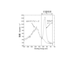
- FIG. 1 shows an example of a Si concentration profile when the Si concentration in the depth direction of the Al bonding wire or Al bonding wire of the present invention is measured and evaluated by XPS. This is a profile of the Si concentration in the depth direction when the total of metal Si and metal Al is 100 atomic %.
- 2 shows an example of the Si2p Si0 valence peak obtained by XPS for the Al bonding wire or Al bonding ribbon of the present invention.
- FIG. 2 is also a diagram for explaining the quantification of Si element based on the Si2p Si0 valence peak.
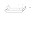
- 3 is a schematic diagram for explaining a measurement target surface (inspection surface) when measuring the crystal orientation of the Al phase and the average diameter of the Si phase of an Al bonding wire.
- the measurement target surface is a cross section (L cross section) in the central axis direction including the central axis of the Al bonding wire.
- 4 is a schematic diagram for explaining the measurement target surface (inspection surface) when measuring the crystal orientation of the Al phase and the average diameter of the Si phase for the Al bonding ribbon.
- the measurement target surface is a cross section (L cross section) in the central axis direction including the central axis of the Al bonding ribbon.
- Al bonding wire or Al bonding ribbon contains 3.0 mass% or more and 20.0 mass% or less of Si, and when the Si concentration (atomic %) in the depth direction from the surface of the Al bonding wire or Al bonding ribbon is measured by X-ray photoelectron spectroscopy (XPS: X-ray Photoelectron Spectroscopy), the ratio Ca/Cb of the average concentration Ca of Si element in a region a having a depth from the surface of 5 nm to 50 nm and the average concentration Cb of Si element in a region b having a depth from the surface of 800 nm to 1200 nm is 0.03 or more and 0.5 or less.
- XPS X-ray Photoelectron spectroscopy
- TCT Temperature Cycle Test
- high-temperature temperature cycle test As mentioned above, next-generation power semiconductor devices with high heat resistance, such as SiC power semiconductor devices, are required to exhibit good temperature cycle reliability even in a high-temperature temperature cycle test that employs such severe test conditions, and further improvement of temperature cycle reliability is required.
- the inventors have found that modifying the surface of an Al bonding wire or Al bonding ribbon is effective in preventing crack growth at the bonding interface, which is a factor in reliability deterioration during high-temperature temperature cycle testing.
- an Al bonding wire or Al bonding ribbon made of an Al alloy with a high concentration of Si added hereinafter also referred to as a "high-concentration Al-Si alloy"
- the surface condition has a greater effect on temperature cycle reliability.
- Al bonding wire or Al bonding ribbon of the present invention exhibits good temperature cycle reliability even in high-temperature temperature cycle tests and also exhibits good 1st bond strength is believed to be as follows.
- a predetermined gradient in the Si concentration in the depth direction i.e., a low Si concentration near the surface and a high Si concentration deep inside, is provided so as to satisfy the above condition of the ratio Ca/Cb.
- the factor that brings about these actions and effects is believed to be the influence of the surface side being relatively softer and more highly purified (in terms of Al concentration) than the deeper parts in the region from the surface of the Al bonding wire or Al bonding ribbon to a certain depth. It is believed that the interfacial control effect of having a constant low concentration gradient of Si concentration on the surface side, and the contribution of the internal Si phase to reducing the difference in linear thermal expansion coefficients and the resulting effect of reducing thermal stress act synergistically, resulting in a remarkable effect of achieving good temperature cycle reliability even in high-temperature temperature cycle tests with an upper limit temperature of 185°C.
- the Al bonding wire or Al bonding ribbon of the present invention has a surface modified to have a predetermined gradient in the Si concentration in the depth direction in the region from the surface to a certain depth. As a result, it is presumed that the Al bonding wire or Al bonding ribbon of the present invention exhibits good temperature cycle reliability even in high-temperature temperature cycle tests as described above, as well as good 1st bond strength.
- Al bonding wire or Al bonding ribbon of the present invention will be described in detail below.
- Al bonding wire and Al bonding ribbon will be collectively referred to as "Al bonding wire, etc.” or “wire, etc.”.
- the Al bonding wire or Al bonding ribbon of the present invention contains Si in an amount of 3.0 mass% or more and 20.0 mass% or less.
- the Si concentration in the range of 3.0 mass% or more and 20.0 mass% or less helps to reduce thermal distortion of the joint and improve temperature cycle characteristics. Specifically, a Si concentration of 3.0 mass% or more can greatly improve temperature cycle reliability even in high-temperature temperature cycle tests.
- a Si concentration of 3.0 mass% or more can greatly improve temperature cycle reliability even in high-temperature temperature cycle tests.
- the upper limit of the Si concentration with the advancement and optimization of the equipment and conditions used in the manufacture and joining of wires, etc., it has become possible to tolerate higher values while suppressing defects such as breakage during processing, deterioration of surface properties, reduction in initial joint strength due to hardening, and damage to semiconductor chips.
- a Si concentration of 20.0 mass% or less can effectively suppress these defects and achieve the desired temperature cycle reliability.
- the concentration of Si in the Al bonding wire etc. of the present invention is 3.0 mass% or more, preferably 3.5 mass% or more, more preferably 4.0 mass% or more, and even more preferably 4.2 mass% or more, 4.4 mass% or more, 4.5 mass% or more, 4.6 mass% or more, 4.8 mass% or more, or 5.0 mass% or more.
- the concentration of Si in the Al bonding wire etc. is 3.0 mass% or more, preferably 3.5 mass% or more, more preferably 4.0 mass% or more, and even more preferably 4.2 mass% or more, 4.4 mass% or more, 4.5 mass% or more, 4.6 mass% or more, 4.8 mass% or more, or 5.0 mass% or more.
- the of the present invention is 20.0 mass% or less, preferably 19.0 mass% or less, 18.0 mass% or less, 17.0 mass% or less, 16.0 mass% or less, 15.0 mass% or less, 14.5 mass% or less, 14.0 mass% or less, 13.5 mass% or less, 13.0 mass% or less, or 12.5 mass% or less. Furthermore, if the hardness of the Al bonding wire etc. is high, depending on the bonding conditions of ultrasonic vibration and load, damage to the semiconductor chip is likely to occur during the first bonding. From the viewpoint of obtaining good bonding strength under a wider range of bonding conditions, the Si concentration in the Al bonding wire etc.
- the present invention is more preferably 12.0 mass% or less, even more preferably 11.5 mass% or less or 11.0 mass% or less, and particularly preferably 10.8 mass% or less, 10.6 mass% or less, 10.5 mass% or less, 10.4 mass% or less, 10.2 mass% or less, or 10.0 mass% or less.
- an ICP (Inductively Coupled Plasma) emission spectrometer or an ICP mass spectrometer can be used. If elements derived from atmospheric contaminants such as oxygen or carbon are adsorbed on the surface of the Al bonding wire, it is effective to clean the wire with an acid or alkali depending on the adsorbed substance before performing the analysis.
- ICP Inductively Coupled Plasma
- the Al bonding wire etc. of the present invention contains 3.0 mass% to 20.0 mass% Si, and is composed of an Al phase in which Si is dissolved in Al, and a Si phase formed by crystallization or precipitation of Si.
- the Al phase may contain other additive elements in addition to Si.
- the Si phase is a general term for Si crystallized material and Si precipitates. Si crystallized material is formed from the molten liquid during solidification and is coarse with a size of about 1 to 25 ⁇ m, whereas Si precipitates are formed from the solid state and are small with a size of about 0.1 to several ⁇ m.
- the Si phase has a smaller linear thermal expansion coefficient than Al, which contributes to reducing the difference in linear thermal expansion coefficient between the Al bonding wire etc. and the semiconductor chip, and can reduce thermal stress, thereby improving temperature cycle reliability.
- the Si concentration (atomic %) in the depth direction from the surface of the Al bonding wire or Al bonding ribbon is measured by X-ray photoelectron spectroscopy (XPS)
- the ratio Ca/Cb of the average Si element concentration Ca in a region a having a depth from the surface of 5 nm or more and 50 nm or less to the average Si element concentration Cb in a region b having a depth from the surface of 800 nm or more and 1200 nm or less is 0.03 or more and 0.5 or less.
- the gradient of the Si concentration in the depth direction is measured and evaluated by X-ray photoelectron spectroscopy (XPS).
- XPS X-ray photoelectron spectroscopy
- the Si concentration is calculated when the total of metallic Si and metallic Al is taken as 100 atomic %.
- Figure 1 shows an example of a Si concentration profile when the Si concentration in the depth direction of the Al bonding wire or Al bonding ribbon of the present invention is measured and evaluated by XPS.
- a certain gradient in the Si concentration in the depth direction is confirmed, i.e., the Si concentration on the surface side is low, the Si concentration in the depth portion is high, and the Si concentration gradually increases in the depth direction.
- the forms of Si detected by XPS include dissolved Si in the Al phase, Si particles (precipitation/crystallization), and intermetallic compounds containing Si.
- the origin of the detected Si may differ, but without distinguishing between these, a judgment is made based on the Si concentration detected by XPS as to whether or not the specified Si concentration gradient (the above ratio Ca/Cb) is met.
- the gradient of the Si concentration in the depth direction measured by XPS can be adjusted to solve and achieve the desired problems and effects.
- the Si concentration is measured by XPS and the concentration determined from the peak of detected metallic Si (Si with a valence of zero) is used. Because the peaks of metallic Si and silicon oxide are detected at different energies, the concentration of metallic Si can be determined separately from silicon oxide.
- the concentration of metallic Si in the surface region of the Al bonding wire or Al bonding ribbon affects the temperature cycle reliability and 1st bond strength. Si oxide rarely forms on the surface of the Al bonding wire or Al bonding ribbon or on the surface of Si particles, and even if it does form, the Si oxide is quite thin. It has been confirmed that it has almost no effect on temperature cycle reliability or 1st bond strength, and is therefore excluded from the analysis target when determining the concentration gradient of the present invention.
- the ratio Ca/Cb of the average Si element concentration Ca in region a from 5 nm to 50 nm deep from the surface to the average Si element concentration Cb in region b from 800 nm to 1200 nm deep from the surface is in the range of 0.03 to 0.5.
- the average concentration Ca of the Si element in the region a having a depth of 5 nm or more and 50 nm or less from the surface is used because the region a is deformed by the ultrasonic vibration and the application of load during bonding, which has a large effect on the performance of the bonding interface.
- the analysis of the outermost surface region having a depth of less than 5 nm from the surface is easily affected by surface contamination, etc., and the variation in the Si concentration measured by XPS is large, so it is excluded from the analysis range.
- the region having a depth of more than 50 nm from the surface is excluded from the analysis range because it has little effect on the bonding interface.
- the average concentration Cb of the Si element in the region b having a depth of 800 nm or more and 1200 nm or less from the surface is used because it is an appropriate depth range for determining the Si concentration that represents the internal composition of the Al bonding wire or Al bonding ribbon, taking into consideration that the Si concentration is almost stable and that the sputtering time during measurement can be avoided to be long, thereby ensuring analytical efficiency.
- the effect of the variation in the Si concentration is minimized by using the average concentration of Si element (Ca and Cb) for the region a with a depth from the surface of 5 nm to 50 nm and for the region b with a depth from the surface of 800 nm to 1200 nm, and then evaluating the gradient of the Si concentration at their ratio Ca/Cb.
- using the average concentration Cb of Si element in the region b inside the sample measured by XPS and calculating the ratio Ca/Cb by comparing it with the average concentration Ca of Si element in the region a on the sample surface measured by the same method is effective in accurately determining the gradient of the Si concentration in the depth direction.
- a ratio Ca/Cb is preferably 0.48 or less, more preferably 0.46 or less, and even more preferably 0.45 or less, 0.44 or less, 0.42 or less, or 0.4 or less.
- the lower limit of the ratio Ca/Cb is 0.03 or more, which can solve or achieve the desired problems and effects, but may also be, for example, 0.04 or more, 0.05 or more, 0.06 or more, 0.08 or more, or 0.1 or more.
- the ratio Ca/Cb is 0.45 or less, it is possible to achieve particularly good temperature cycle reliability even in high-temperature temperature cycle tests, and it is preferable because it is easy to achieve even better 1st bonding strength.
- the present invention by controlling the above-mentioned ratio Ca/Cb, which is the relative ratio of the Si concentration near the surface to the deep portion, within a certain range of 0.03 to 0.5, it has become possible to realize an Al bonding wire or Al bonding ribbon that exhibits good temperature cycle reliability even in high-temperature temperature cycle tests and exhibits good 1st bond strength, and it has been discovered that controlling such a ratio Ca/Cb within a certain range is effective and important in solving the problem.
- the ratio Ca/Cb which is the relative ratio of the Si concentration near the surface to the deep portion
- the Si concentration in the depth direction in a region from the surface of the Al bonding wire or Al bonding ribbon to a certain depth can be measured by performing composition analysis by XPS while digging in the depth direction (towards the center of the wire, etc.) from the surface of the Al bonding wire or Al bonding ribbon by Ar sputtering.
- composition analysis by XPS while digging in the depth direction (towards the center of the wire, etc.) from the surface of the Al bonding wire or Al bonding ribbon by Ar sputtering.
- concentration profile in the depth direction can be measured by performing composition analysis by XPS while digging in the depth direction (towards the center of the wire, etc.) from the surface of the Al bonding wire or Al bonding ribbon by Ar sputtering.
- the Si concentration in the depth direction in a region from the surface of the Al bonding wire or Al bonding ribbon of the present invention to a certain depth is measured by the following steps (1) to (4).
- the Al bonding wire or Al bonding ribbon sample to be measured is placed on the sample stage. At that time, the position is adjusted so that the longitudinal direction of the sample is horizontal on the operation screen of the XPS device. If the sample is an Al bonding ribbon (having a rectangular or nearly rectangular cross-sectional shape with width W and thickness T), it is placed so that the width W direction is parallel to the surface of the sample stage and the thickness T direction is perpendicular to the surface of the sample stage.
- the measurement area is selected so that the vicinity of the apex of the sample of the Al bonding wire or Al bonding ribbon is the measurement area while watching the screen of the SXI (Scanning X-ray Image) of the device.
- the apex of the sample of the Al bonding wire or Al bonding ribbon is the point directly above the central axis of the sample when the sample is observed from directly above.
- Measurement device ULVAC-PHI Versa Probe 3 ⁇ Ultimate vacuum level: Approximately 1 ⁇ 10 -8 Torr X-ray source: monochromatic Al (1486.6 eV) Measurement area: 100 ⁇ m (longitudinal direction of sample) x 20 ⁇ m (circumferential direction of sample) square Photoelectron take-off angle: 45 degrees Detection depth: several nm Ar sputtering Acceleration voltage: 2 kV Sputtering area: 2 x 2 mm square Sputtering rate: 9.2 nm/min ( SiO2 equivalent) Analysis pitch in the depth direction: 5 nm pitch (depth from the surface range of 0 to 50 nm), 10 nm pitch (depth from the surface range of 50 to 200 nm), 20 nm pitch (depth from the surface range of more than 200
- the scale of the sputtering rate and depth can be calculated in general SiO2 conversion.
- the analysis pitch in the depth direction can be selected to be fine at the surface and coarse at the deep part, taking into consideration the accuracy of the analysis, the measurement time, the workability, etc.
- the pitch can be 5 nm for the range of 0 to 50 nm from the surface, 10 nm for the range of 50 to 200 nm from the surface, and 200 nm for the range of over 200 nm from the surface.
- the Si element is quantified in the energy quantification range (about 95.0 to 101.0 eV) including the peak of Si0 valence (metallic Si) of Si2p.
- the energy values of the low energy end and the high energy end were adjusted within the quantification range according to the shape of the peak.
- the background of the quantification range is determined using the Shirley method, and the Si element is quantified based on the peak area after subtracting the background.
- Figure 2 shows an example of a Si2p Si0 valence peak obtained by XPS for the Al bonding wire or Al bonding ribbon of the present invention.
- the Si2p Si0 valence peak is included in the quantitative range of approximately 95.0 to 101.0 eV, and the low energy end of the peak can be selected between 95 to 96.5 eV and the high energy end between 99.8 to 101.3 eV.
- Quantitative analysis of Al element is performed using the same procedure as for quantification of Si element above, for the quantitative energy range (approximately 69.0 to 79.0 eV) that includes the peak of Al0 valence (metallic Al) of Al2p.
- the Si concentration (atomic %) is calculated when the total of Si and Al at each depth position from the surface of the sample in the depth direction is 100 atomic %. Note that the C element affected by contaminants on the surface of the sample is excluded from the analysis.
- the arithmetic average value of the Si concentration in the region a from 5 nm to 50 nm deep from the surface is calculated as the average concentration Ca
- the arithmetic average value of the Si concentration in the region b from 800 nm to 1200 nm deep from the surface is calculated as the average concentration Cb
- the arithmetic average value of the Si concentration in the region f from 5 nm to 30 nm deep from the surface is calculated as the average concentration Cf.
- the gradient of the Si concentration in the depth direction and the average concentration of Si element near the surface are evaluated by averaging (arithmetic mean) the values obtained by measuring two or more locations.
- averaging arithmetic mean
- the average concentration Ca, average concentration Cb, and average concentration Cf are the average values (arithmetic mean) of the values obtained for each sample by the above steps (1) to (4).
- the average concentration Cf of Si element in a region f having a depth from the surface of 5 nm or more to 30 nm or less is 0.1 atomic % or more and 4 atomic % or less.
- the life (number of cycles until failure occurs) of the Al bonding wire or Al bonding ribbon can be further improved in a high-temperature temperature cycle test.
- the average concentration Cf low to the above range, it is possible to soften the surface of the Al bonding wire, promote recrystallization, improve deformability during bonding, and form a flat bonding interface, and as a result, it is believed that the life of the Al bonding wire, etc. can be further improved in a high-temperature temperature cycle test. From the viewpoint of further improving the life of the Al bonding wire, etc.
- the average concentration Cf of Si element near the surface is lower than the Si concentration Ct in the entire Al bonding wire or Al bonding ribbon, the above-mentioned life improvement effect can be further improved.
- the ratio Cf/Ct of the surface concentration Cf of Si element to the Si concentration Ct in the entire Al bonding wire or Al bonding ribbon is preferably in the range of 0.03 to 0.8.
- the Si concentration Ct is based on the Si concentration in the entire Al bonding wire or Al bonding ribbon measured using an ICP optical emission spectrometer or an ICP mass spectrometer.
- the ratio Cf/Ct is more preferably 0.7 or less, even more preferably 0.6 or less, 0.55 or less, or 0.5 or less.
- the lower limit of the ratio Cf/Ct is preferably 0.03 or more, but may be, for example, 0.04 or more, 0.05 or more, 0.06 or more, 0.08 or more, or 0.1 or more.
- the gradient of the Si concentration in the depth direction and the concentration of the Si element near the surface are measured and evaluated by XPS.
- XPS X-ray photoelectron spectroscopy
- the Al bonding wire or Al bonding ribbon of the present invention preferably has an average diameter of the Si phase in its L cross section (cross section in the central axis direction including the central axis) of 0.8 ⁇ m or more and 4 ⁇ m or less.
- FIG. 3 shows the case of an Al bonding wire having a circular cross section, but in the case of an Al bonding ribbon having a rectangular or approximately rectangular cross section with width W and thickness T, the central axis refers to the axis passing through the center of width W and the center of thickness T, and the L cross section refers to a cross section in the central axis direction including the central axis and in the direction of thickness T (FIG. 4).
- the cross section when processing the cross section to expose the L cross section of the Al bonding wire, it may deviate from the central axis of the Al bonding wire.
- the length of the L cross section in the direction perpendicular to the central axis is 90% or more of the wire diameter of the Al bonding wire, it can be considered as a cross section including the central axis.
- the Si that exists beyond the solid solubility of Si exists as Si particles due to crystallization or precipitation. If the Si particles become coarse, cracks will occur at the ends of the Si particles during high-temperature temperature cycle tests, causing a decrease in the fatigue resistance of the surface region of the Al bonding wire or Al bonding ribbon.
- the average diameter of the Si phase in the L cross section to a relatively small particle size between 0.8 ⁇ m and 4 ⁇ m, the thermal fatigue resistance of the Si particles in the surface region can be improved.
- the Si content is 3.0% by mass or more and 20.0% by mass or less, and the Si concentration in the depth direction from the surface is measured by XPS, the ratio Ca/Cb of the average concentration of Si element in the region a from the surface to a depth of 5 nm to 50 nm and the average concentration of Si element in the region b from the surface to a depth of 800 nm to 1200 nm is in the range of 0.03 to 0.5.
- the average diameter of the Si phase in the L cross section is in the range of 0.8 ⁇ m to 4 ⁇ m, so that better temperature cycle reliability can be achieved in high-temperature temperature cycle tests.
- the Si concentration gradient in the region from the surface to a certain depth is combined with the small grain size Si phase, a synergistic effect is obtained regarding the control of the bonding interface and the reduction of thermal distortion, which are the respective effects, and the effect of improving the temperature cycle reliability in high-temperature temperature cycle tests can be further enhanced. Furthermore, since the Si phase has a lower linear thermal expansion coefficient than Al, the Si phase present inside the surface region reduces the linear thermal expansion coefficient of the entire Al bonding wire or Al bonding ribbon, thereby improving temperature cycle reliability.
- the average diameter of the Si phase in the L-section of the Al bonding wire or Al bonding ribbon of the present invention is more preferably 3.8 ⁇ m or less or 3.5 ⁇ m or less, even more preferably 3.4 ⁇ m or less, 3.2 ⁇ m or less, or 3 ⁇ m or less, and the lower limit is more preferably 1 ⁇ m or more, even more preferably 1.1 ⁇ m or more, even more preferably 1.2 ⁇ m or more, or 1.5 ⁇ m or more.
- a method for measuring the average diameter of the Si phase in the L cross section of the Al bonding wire or Al bonding ribbon will be described.
- the average diameter of the Si phase in the L cross section can be measured using a SEM-EDS-EBSD device.
- SEM-EDS Sccanning Electron Microscope-Energy Dispersive X-ray Spectroscopy
- EBSD electron backscatter diffraction
- the Al phase and the Si phase are separated and extracted from the EDS measurement results using the analysis software attached to the device.
- the Chi Scan function which is a function of the analysis software OIM Data Collection or OIM Analysis (both made by TSL Solutions) attached to the FE-SEM (Field Emission-Scanning Electron Microscope) device.
- the crystal orientation can be analyzed by using the analysis software attached to the device. If the orientation difference between the measurement points is 15° or more, it is determined to be a grain boundary and the circle equivalent diameter is calculated. The average value of the circle equivalent diameter of each Si phase is defined as the average diameter of the Si phase.
- the average diameter of the Si phase in the L cross section of the Al bonding wire or Al bonding ribbon of the present invention is calculated by the following steps (1) to (3).
- (1) The L-section of an Al bonding wire or an Al bonding ribbon is used as the inspection surface, and the Al and Si concentrations are measured using EDS and the crystal orientation is measured using EBSD at the same time.
- the crystal orientation can be analyzed using the Al and Si crystal information in the material file.
- the crystal orientation is analyzed, and if the orientation difference between the measurement points is 15° or more, it is determined to be a grain boundary, and the circle equivalent diameter of each crystal grain is calculated.
- the circle equivalent diameters of each crystal grain are then averaged to calculate the average diameter of the Si phase.
- the average value obtained by area average area weighted average
- the area average the ratio of each particle area to the area of all particles is multiplied by each particle area value, and the software automatically calculates it.
- the Tolerance (%) setting can be selected in the range of 20-40%, and in standard analysis of the L-section of an Al bonding wire or Al bonding ribbon, it is preferable to compare at about 30%.
- the procedure for adjusting this Tolerance It is preferable to select or confirm the Tolerance value so that the shape and size of the Si phase extracted and identified by the Chi Scan function are equivalent to those of the Si phase identified from the EDS map, which displays the Si element concentration in EDS analysis in two dimensions.
- the average diameter of the Si phase in the L cross section is the average (arithmetic mean) of the values obtained by measuring at three or more locations.
- the measurement area from the viewpoint of ensuring the objectivity of the measurement data, it is preferable to obtain measurement samples from the Al bonding wire or Al bonding ribbon to be measured at intervals of 50 cm or more along the central axis of the Al bonding wire or Al bonding ribbon, and provide them for measurement.
- the measurement area in the L cross section by the EBSD method is a length in the central axis direction of the Al bonding wire or Al bonding ribbon of 300 ⁇ m or more and less than 800 ⁇ m, and it is desirable that the entire Al bonding wire or Al bonding ribbon is included in the direction perpendicular to the central axis of the Al bonding wire or Al bonding ribbon, but if the size is large and it is difficult to measure the entire area, it can be adjusted to a range of less than 600 ⁇ m.
- the orientation ratio of the ⁇ 100> crystal orientation with an angle difference of 15° or less with respect to the direction parallel to the central axis (RD direction) (hereinafter also referred to as the "orientation ratio of the ⁇ 100> crystal orientation of the Al phase in the RD direction") is preferably 15% or more and 50% or less. If the orientation ratio of the ⁇ 100> crystal orientation of the Al phase in the RD direction is within the above range, a better initial bonding strength (1st bonding strength) of the 1st bonding portion can be realized.
- the ratio Ca/Cb of the average Si element concentration Ca in the region a from the surface to a depth of 5 nm or more and 50 nm or less to the average Si element concentration Cb in the region b from the surface to a depth of 800 nm or more and 1200 nm or less is in the range of 0.03 to 0.5.
- the orientation ratio of the ⁇ 100> crystal orientation of the Al phase in the RD direction in the L cross section is in the range of 15% to 50%, so that even better 1st bond strength can be realized.
- the effect of controlling the bond interface by the gradient of the Si concentration in the region from the surface to a certain depth and the effect of the orientation of the ⁇ 100> crystal orientation of the Al phase in the RD direction are obtained synergistically, so that the effect of improving the 1st bond strength can be further enhanced, and as a result, it can also contribute to improving temperature cycle reliability in high-temperature temperature cycle tests.
- the orientation ratio of the ⁇ 100> crystal orientation of the Al phase in the RD direction in the L cross section of the Al bonding wire or Al bonding ribbon of the present invention is more preferably 20% or more, even more preferably 22% or more, 24% or more, 26% or more, or 28% or more, and even more preferably 30% or more, or 35% or more.
- the upper limit of the orientation ratio of the ⁇ 100> crystal orientation of the Al phase in the RD direction is more preferably 48% or less, or 45% or less, even more preferably 42% or less, and even more preferably 40% or less.
- a method for measuring the orientation ratio of the crystal orientation of the Al phase in the L cross section of an Al bonding wire or an Al bonding ribbon will be described.
- the orientation ratio of the crystal orientation of the Al phase in the L cross section can be measured using a SEM-EDS-EBSD device, similar to the measurement of the average diameter of the Si phase described above.
- a method can be used in which the information on the Al concentration and Si concentration obtained by SEM-EDS and the information on the crystal orientation obtained by EBSD are combined.
- a more detailed procedure may be the same as that described above in relation to the measurement of the average diameter of the Si phase.
- the orientation ratio of the ⁇ 100> crystal orientation of the Al phase in the RD direction can be calculated by using the analysis software attached to the device.
- a partial ratio calculated as a population of the area of only the crystal orientations that could be identified based on a certain reliability within the measurement area is used.
- the area ratio of the ⁇ 100> crystal orientation in the RD direction with respect to the crystal orientation of the Al phase was taken as the orientation ratio of the ⁇ 100> crystal orientation in the RD direction. Therefore, in one embodiment, the orientation ratio of the crystal orientation of the Al phase in the L cross section of the Al bonding wire or Al bonding ribbon of the present invention is calculated by the following steps (1) to (3).
- the Al and Si concentrations are measured using EDS, and the crystal orientation is measured using EBSD at the same time.
- Al and Si are separated and extracted. Specifically, by setting the tolerance equivalent to the Si threshold from the Si EDS measurement results, Al and Si can be separated and identified. The crystal orientation can be analyzed using the Al and Si crystal information in the material file.
- the crystal orientation is analyzed, and the orientation ratio of the ⁇ 100> crystal orientation of the Al phase in the RD direction is calculated.
- the Tolerance setting range in step (2) above the method of obtaining the sample for measurement, and the measurement area of the crystal orientation using the EBSD method are as described above for measuring the average diameter of the Si phase.
- the Al bonding wire or Al bonding ribbon of the present invention may further contain one or more of Sr, Na, P, and B (hereinafter also referred to as the "first element group").
- the total concentration of the first element group may be 0 ppm by mass, preferably 1 ppm by mass or more, more preferably 3 ppm by mass or more, even more preferably 5 ppm by mass or more, particularly preferably 8 ppm by mass or more or 10 ppm by mass or more.
- the upper limit of the total concentration of the first element group is preferably 10,000 ppm by mass or less or 8,000 ppm by mass or less, more preferably 5,000 ppm by mass or less or 3,000 ppm by mass or less, even more preferably 2,000 ppm by mass or less or 1,000 ppm by mass or less, particularly preferably 900 ppm by mass or less or 800 ppm by mass or less.
- the total concentration of the first element group is preferably 10 ppm by mass or more and 800 ppm by mass or less.
- the Al bonding wire or Al bonding ribbon of the present invention further contains at least one of Sr, Na, P, and B in a total amount of 10 mass ppm to 800 mass ppm, thereby reducing the frequency of wire breakage during wire drawing of the Al bonding wire or Al bonding ribbon.
- Al alloys containing a high concentration of Si, 3.0 mass% to 20.0 mass% tend to have a higher frequency of wire breakage during wire drawing.
- particles of the Si phase crystallized during solidification cause stress concentration during wire drawing, inducing wire breakage.
- the addition of the first element group can distribute the particulate Si phase uniformly and suppress the growth and coarsening of the Si phase, thereby easing stress concentration during wire drawing and reducing wire breakage.
- the total concentration of the first element group in the Al bonding wire or Al bonding ribbon of the present invention is more preferably 20 mass ppm or more, even more preferably 30 mass ppm or more, 40 mass ppm or more, or 50 mass ppm or more, and the upper limit is preferably 750 mass ppm or less, more preferably 740 mass ppm or less, 720 mass ppm or less, or 700 mass ppm or less, even more preferably 680 mass ppm or less, 650 mass ppm or less, 620 mass ppm or less, or 600 mass ppm or less, and particularly preferably 580 mass ppm or less, 550 mass ppm or less, 520 mass ppm or less, or 500 mass ppm or less.
- the Al bonding wire or Al bonding ribbon of the present invention may contain one of the first element group, two of the first element group, three of the first element group, or all four of the first element group. Also, when the Al bonding wire or Al bonding ribbon of the present invention contains one or more of the first element group, it may contain Sr, Na, P, or B.
- the concentration of Sr may be 0 ppm by mass, and is preferably 1 ppm by mass or more, 3 ppm by mass or more, 5 ppm by mass or more, or 8 ppm by mass or more.
- the concentration of Sr is more preferably 10 ppm by mass or more, and even more preferably 20 ppm by mass or more, 30 ppm by mass or more, 40 ppm by mass or more, or 50 ppm by mass or more.
- the upper limit of the concentration of Sr is preferably 10,000 ppm by mass or less, 8,000 ppm by mass or less, 5,000 ppm by mass or less, 3,000 ppm by mass or less, 2,000 ppm by mass or less, 1,000 ppm by mass or less, or 900 ppm by mass or less.
- the Sr concentration is more preferably 800 ppm by mass or less, even more preferably 750 ppm by mass or less, 740 ppm by mass or less, 720 ppm by mass or less, 700 ppm by mass or less, 680 ppm by mass or less, 650 ppm by mass or less, 620 ppm by mass or less, 600 ppm by mass or less, 580 ppm by mass or less, 550 ppm by mass or less, 520 ppm by mass or less, or 500 ppm by mass or less.
- the Na concentration may be 0 ppm by mass, and is preferably 1 ppm by mass or more, 3 ppm by mass or more, 5 ppm by mass or more, or 8 ppm by mass or more.
- the Na concentration is more preferably 10 ppm by mass or more, and even more preferably 20 ppm by mass or more, 30 ppm by mass or more, 40 ppm by mass or more, or 50 ppm by mass or more.
- the upper limit of the Na concentration is preferably 10,000 ppm by mass or less, 8,000 ppm by mass or less, 5,000 ppm by mass or less, 3,000 ppm by mass or less, 2,000 ppm by mass or less, 1,000 ppm by mass or less, or 900 ppm by mass or less.
- the Na concentration is more preferably 800 ppm by mass or less, even more preferably 750 ppm by mass or less, 740 ppm by mass or less, 720 ppm by mass or less, 700 ppm by mass or less, 680 ppm by mass or less, 650 ppm by mass or less, 620 ppm by mass or less, 600 ppm by mass or less, 580 ppm by mass or less, 550 ppm by mass or less, 520 ppm by mass or less, or 500 ppm by mass or less.
- the concentration of P may be 0 ppm by mass, and is preferably 1 ppm by mass or more, 3 ppm by mass or more, 5 ppm by mass or more, or 8 ppm by mass or more.
- the concentration of P is more preferably 10 ppm by mass or more, and even more preferably 20 ppm by mass or more, 30 ppm by mass or more, 40 ppm by mass or more, or 50 ppm by mass or more.
- the upper limit of the concentration of P is preferably 10,000 ppm by mass or less, 8,000 ppm by mass or less, 5,000 ppm by mass or less, 3,000 ppm by mass or less, 2,000 ppm by mass or less, 1,000 ppm by mass or less, or 900 ppm by mass or less.
- the P concentration is more preferably 800 ppm by mass or less, even more preferably 750 ppm by mass or less, 740 ppm by mass or less, 720 ppm by mass or less, 700 ppm by mass or less, 680 ppm by mass or less, 650 ppm by mass or less, 620 ppm by mass or less, 600 ppm by mass or less, 580 ppm by mass or less, 550 ppm by mass or less, 520 ppm by mass or less, or 500 ppm by mass or less.
- the concentration of B may be 0 ppm by mass, and is preferably 1 ppm by mass or more, 3 ppm by mass or more, 5 ppm by mass or more, or 8 ppm by mass or more.
- the concentration of B is more preferably 10 ppm by mass or more, and even more preferably 20 ppm by mass or more, 30 ppm by mass or more, 40 ppm by mass or more, or 50 ppm by mass or more.
- the upper limit of the concentration of B is preferably 10,000 ppm by mass or less, 8,000 ppm by mass or less, 5,000 ppm by mass or less, 3,000 ppm by mass or less, 2,000 ppm by mass or less, 1,000 ppm by mass or less, or 900 ppm by mass or less.
- the concentration of B is more preferably 800 ppm by mass or less, even more preferably 750 ppm by mass or less, 740 ppm by mass or less, 720 ppm by mass or less, 700 ppm by mass or less, 680 ppm by mass or less, 650 ppm by mass or less, 620 ppm by mass or less, 600 ppm by mass or less, 580 ppm by mass or less, 550 ppm by mass or less, 520 ppm by mass or less, or 500 ppm by mass or less.
- the Al bonding wire or Al bonding ribbon of the present invention may further contain one or more of Ni, Ti, Fe, Zn, and Mg (hereinafter also referred to as the "second element group").
- the total concentration of the second element group may be 0 mass ppm, preferably 1 mass ppm or more or 3 mass ppm or more, more preferably 5 mass ppm or more or 8 mass ppm or more, even more preferably 10 mass ppm or more or 30 mass ppm or more, particularly preferably 50 mass ppm or more, 80 mass ppm or more, or 100 mass ppm or more.
- the upper limit of the total concentration of the second element group is preferably 10,000 mass ppm or less, more preferably 8,000 mass ppm or less, even more preferably 5,000 mass ppm or less, particularly preferably 3,000 mass ppm or less or 2,000 mass ppm or less. In one embodiment, the total concentration of the second element group is preferably 100 mass ppm or more and 2,000 mass ppm or less.
- the Al bonding wire or Al bonding ribbon of the present invention further contains at least one of Ni, Ti, Fe, Zn, and Mg in a total amount of 100 mass ppm to 2000 mass ppm, thereby suppressing the occurrence of scratches and abrasions on the surface of the Al bonding wire or Al bonding ribbon and forming a smooth surface.
- An Al alloy containing Si at a high concentration of 3.0 mass% to 20.0 mass% may cause scratches and abrasions on the surface during wire drawing due to hardening of the surface and the loss of Si phase and Al oxide present on the surface, resulting in an Al bonding wire or Al bonding ribbon with large surface irregularities.
- the addition of the second element group stabilizes the Al oxide on the surface of the Al bonding wire or Al bonding ribbon, refines the structure of the Al crystal grains, and hardens it, thereby reducing scratches and abrasions during wire drawing.
- the occurrence of scratches and abrasions on the surface of the Al bonding wire or Al bonding ribbon can be suppressed, enhancing the effect of forming a smooth surface.
- the total concentration of the second element group in the Al bonding wire or Al bonding ribbon of the present invention is more preferably 150 mass ppm or more, even more preferably 200 mass ppm or more, 250 mass ppm or more, or 300 mass ppm or more, and the upper limit is preferably 1800 mass ppm or less, more preferably 1600 mass ppm or less, 1500 mass ppm or less, or 1200 mass ppm or less, even more preferably 1000 mass ppm or less, 900 mass ppm or less, or 800 mass ppm or less, and particularly preferably 700 mass ppm or less, 600 mass ppm or less, or 500 mass ppm or less.
- the Al bonding wire or Al bonding ribbon of the present invention may contain one of the second element group, two of the second element group, three of the second element group, four of the second element group, or all five of the second element group. Also, when the Al bonding wire or Al bonding ribbon of the present invention contains one or more of the second element group, it may contain Ni, Ti, Fe, Zn, or Mg.
- the Ni concentration may be 0 mass ppm, and is preferably 1 mass ppm or more, 3 mass ppm or more, 5 mass ppm or more, 8 mass ppm or more, 10 mass ppm or more, 30 mass ppm or more, 50 mass ppm or more, or 80 mass ppm or more.
- the Ni concentration is more preferably 100 mass ppm or more, and even more preferably 150 mass ppm or more, 200 mass ppm or more, 250 mass ppm or more, or 300 mass ppm.
- the upper limit of the Mn concentration is preferably 10,000 mass ppm or less, 8,000 mass ppm or less, 5,000 mass ppm or less, or 3,000 mass ppm or less.
- the Ni concentration is more preferably 2000 mass ppm or less, even more preferably 1800 mass ppm or less, 1600 mass ppm or less, 1500 mass ppm or less, 1200 mass ppm or less, 1000 mass ppm or less, 900 mass ppm or less, 800 mass ppm or less, 700 mass ppm or less, 600 mass ppm or less, or 500 mass ppm or less.
- the Ti concentration may be 0 mass ppm, and is preferably 1 mass ppm or more, 3 mass ppm or more, 5 mass ppm or more, 8 mass ppm or more, 10 mass ppm or more, 30 mass ppm or more, 50 mass ppm or more, or 80 mass ppm or more.
- the Ti concentration is more preferably 100 mass ppm or more, and even more preferably 150 mass ppm or more, 200 mass ppm or more, 250 mass ppm or more, or 300 mass ppm.
- the upper limit of the Ti concentration is preferably 10,000 mass ppm or less, 8,000 mass ppm or less, 5,000 mass ppm or less, or 3,000 mass ppm or less.
- the Ti concentration is more preferably 2000 mass ppm or less, even more preferably 1800 mass ppm or less, 1600 mass ppm or less, 1500 mass ppm or less, 1200 mass ppm or less, 1000 mass ppm or less, 900 mass ppm or less, 800 mass ppm or less, 700 mass ppm or less, 600 mass ppm or less, or 500 mass ppm or less.
- the concentration of Fe may be 0 ppm by mass, and is preferably 1 ppm by mass or more, 3 ppm by mass or more, 5 ppm by mass or more, 8 ppm by mass or more, 10 ppm by mass or more, 30 ppm by mass or more, 50 ppm by mass or more, or 80 ppm by mass or more.
- the concentration of Fe is more preferably 100 ppm by mass or more, and even more preferably 150 ppm by mass or more, 200 ppm by mass or more, 250 ppm by mass or more, or 300 ppm by mass.
- the upper limit of the concentration of Fe is preferably 10,000 ppm by mass or less, 8,000 ppm by mass or less, 5,000 ppm by mass or less, or 3,000 ppm by mass or less.
- the Fe concentration is more preferably 2000 mass ppm or less, even more preferably 1800 mass ppm or less, 1600 mass ppm or less, 1500 mass ppm or less, 1200 mass ppm or less, 1000 mass ppm or less, 900 mass ppm or less, 800 mass ppm or less, 700 mass ppm or less, 600 mass ppm or less, or 500 mass ppm or less.
- the concentration of Zn may be 0 mass ppm, and is preferably 1 mass ppm or more, 3 mass ppm or more, 5 mass ppm or more, 8 mass ppm or more, 10 mass ppm or more, 30 mass ppm or more, 50 mass ppm or more, or 80 mass ppm or more.
- the concentration of Zn is more preferably 100 mass ppm or more, even more preferably 150 mass ppm or more, 200 mass ppm or more, 250 mass ppm or more, or 300 mass ppm.
- the upper limit of the concentration of Zn is preferably 10,000 mass ppm or less, 8,000 mass ppm or less, 5,000 mass ppm or less, or 3,000 mass ppm or less.
- the Zn concentration is more preferably 2000 mass ppm or less, even more preferably 1800 mass ppm or less, 1600 mass ppm or less, 1500 mass ppm or less, 1200 mass ppm or less, 1000 mass ppm or less, 900 mass ppm or less, 800 mass ppm or less, 700 mass ppm or less, 600 mass ppm or less, or 500 mass ppm or less.
- the concentration of Mg may be 0 mass ppm, and is preferably 1 mass ppm or more, 3 mass ppm or more, 5 mass ppm or more, 8 mass ppm or more, 10 mass ppm or more, 30 mass ppm or more, 50 mass ppm or more, or 80 mass ppm or more.
- the concentration of Mg is more preferably 100 mass ppm or more, even more preferably 150 mass ppm or more, 200 mass ppm or more, 250 mass ppm or more, or 300 mass ppm.
- the upper limit of the Mg concentration is preferably 10,000 mass ppm or less, 8,000 mass ppm or less, 5,000 mass ppm or less, or 3,000 mass ppm or less.
- the Mg concentration is more preferably 2000 mass ppm or less, even more preferably 1800 mass ppm or less, 1600 mass ppm or less, 1500 mass ppm or less, 1200 mass ppm or less, 1000 mass ppm or less, 900 mass ppm or less, 800 mass ppm or less, 700 mass ppm or less, 600 mass ppm or less, or 500 mass ppm or less.
- Al bonding wire or Al bonding ribbon of the present invention it is preferable to use Al with a purity of 4N (Al: 99.99% by mass or more) as the aluminum raw material, and it is even more preferable to use Al with a purity of 5N (Al: 99.999% by mass or more) or more, which has a lower amount of impurities.
- Al with a purity of 3N (Al: 99.9% by mass or more) may be used.
- the Al bonding wire or Al bonding ribbon of the present invention may further contain elements other than Al, Si, the first element group, and the second element group (hereinafter also referred to as "other elements”). That is, “other elements” are elements other than Al, Si, Sr, Na, P, B, Ni, Ti, Fe, Zn, and Mg, and the Al bonding wire or Al bonding ribbon of the present invention may further contain elements other than Al, Si, Sr, Na, P, B, Ni, Ti, Fe, Zn, and Mg.
- the total concentration of other elements in the Al bonding wire or Al bonding ribbon is not particularly limited as long as it does not impair the effects of the present invention.
- the total concentration of the other elements may be, for example, 0.5% by mass or less, 0.4% by mass or less, 0.3% by mass or less, 0.2% by mass or less, 0.15% by mass or less, 0.1% by mass or less, 0.08% by mass or less, 0.06% by mass or less, 0.05% by mass or less, 0.04% by mass or less, 0.03% by mass or less, 0.025% by mass or less, 0.02% by mass or less, 0.018% by mass or less, 0.016% by mass or less, 0.015% by mass or less, 0.014% by mass or less, 0.012% by mass or less, or 0.01% by mass or less.
- the lower limit of the total concentration of the other elements is not particularly limited and may be 0% by mass.
- the remainder of the Al bonding wire or Al bonding ribbon of the present invention consists of Al and other elements.
- the Al bonding wire or Al bonding ribbon of the present invention consists of Al, Si, and other elements.
- the Al bonding wire or Al bonding ribbon of the present invention consists of Al, Si, one or more elements from the first element group, and other elements.
- the Al bonding wire or Al bonding ribbon of the present invention consists of Al, Si, one or more elements from the second element group, and other elements.
- the Al bonding wire or Al bonding ribbon of the present invention consists of Al, Si, one or more elements from the first element group, one or more elements from the second element group, and other elements.
- the remainder of the Al bonding wire or Al bonding ribbon of the present invention consists of Al and unavoidable impurities. Therefore, in a preferred embodiment, the Al bonding wire or Al bonding ribbon of the present invention consists of Al, Si, and unavoidable impurities. In another preferred embodiment, the Al bonding wire or Al bonding ribbon of the present invention consists of Al, Si, one or more elements of the first element group, and unavoidable impurities. In yet another preferred embodiment, the Al bonding wire or Al bonding ribbon of the present invention consists of Al, Si, one or more elements of the second element group, and unavoidable impurities. In yet another preferred embodiment, the Al bonding wire or Al bonding ribbon of the present invention consists of Al, Si, one or more elements of the first element group, one or more elements of the second element group, and unavoidable impurities.
- the Al bonding wire or Al bonding ribbon of the present invention does not have a coating whose main component is a metal other than Al on the outer periphery of the Al bonding wire or Al bonding ribbon.
- a coating whose main component is a metal other than Al refers to a coating whose content of a metal other than Al is 50 mass% or more.
- the Al bonding wire or Al bonding ribbon of the present invention may be an Al bonding wire or an Al bonding ribbon.
- the wire diameter is not particularly limited and may be, for example, 50 ⁇ m or more, 60 ⁇ m or more, 80 ⁇ m or more, 100 ⁇ m or more, 120 ⁇ m or more, 140 ⁇ m or more, 150 ⁇ m or more, 180 ⁇ m or more, or 200 ⁇ m or more.
- the upper limit of the wire diameter is not particularly limited and may be, for example, 600 ⁇ m or less, 550 ⁇ m or less, 500 ⁇ m or less, 450 ⁇ m or less, or 400 ⁇ m or less.
- the wire diameter of the Al bonding wire of the present invention may be in the range of 100 to 600 ⁇ m, and preferably in the range of 200 to 400 ⁇ m.
- the dimensions of its rectangular or nearly rectangular cross section are not particularly limited; for example, W may be 100 to 3000 ⁇ m, and T may be 50 to 600 ⁇ m.
- the Al bonding wire or Al bonding ribbon of the present invention can provide excellent temperature cycle reliability even in high-temperature temperature cycle tests. Therefore, the Al bonding wire or Al bonding ribbon of the present invention can be suitably used as an Al bonding wire or Al bonding ribbon for semiconductor devices.
- the Al bonding wire or Al bonding ribbon of the present invention can be particularly suitably used as an Al bonding wire or Al bonding ribbon for power semiconductor devices, and can be more suitably used as an Al bonding wire or Al bonding ribbon for next-generation power semiconductor devices such as SiC power semiconductor devices.
- the Al and alloying elements used as raw materials preferably have a high purity.
- the Al has a purity of 99.5% by mass or more, with the remainder being composed of inevitable impurities, more preferably a purity of 99.9% by mass or more, with the remainder being composed of inevitable impurities, and even more preferably a purity of 99.99% by mass or more, with the remainder being composed of inevitable impurities.
- the Si, first element group, second element group, and other elements used as alloying elements have a purity of 99.9% by mass or more, with the remainder being composed of inevitable impurities, and more preferably a purity of 99.99% by mass or more, with the remainder being composed of inevitable impurities.
- the Al alloy used for the Al bonding wire can be produced by loading the Al raw material and the raw material of the alloying elements into a graphite or alumina crucible processed to obtain a cylindrical ingot, and melting them using an electric furnace or a high-frequency heating furnace.
- the diameter of the cylindrical ingot is preferably ⁇ 6 mm or more and less than 8 mm, taking into account the workability in the subsequent processing steps.
- the atmosphere in the furnace during melting is preferably an inert atmosphere or a reducing atmosphere to prevent excessive oxidation of Al, Si, the first element group, the second element group, and other elements that make up the wire.
- the maximum temperature that the molten metal reaches during melting is preferably in the range of 700°C or higher and lower than 1050°C, taking into consideration factors such as ensuring the fluidity of the molten metal while making it easier to control the size of the Si phase during solidification.
- Water cooling, furnace cooling, air cooling, etc. can be used as a cooling method during solidification.
- the cylindrical ingot obtained by melting is subjected to solution treatment by heating at high temperatures, and then repeatedly drawn using a die to produce wire of the desired diameter. After the drawing process, the wire is subjected to final heat treatment in an electric furnace so that it can be used as Al bonding wire.
- Control of Si concentration gradient In order to control the gradient of the Si concentration in the region from the surface to a certain depth, it is effective to control the wire feed speed (wire drawing speed) in the wire drawing process, the die area reduction rate, the lubricity at the contact interface between the wire and the die, and the atmosphere of the intermediate heat treatment.
- An example of the manufacturing conditions for providing a predetermined gradient in the Si concentration in the depth direction in the region from the surface to a certain depth i.e., for controlling the above ratio Ca/Cb to be in the range of 0.03 to 0.5 is shown below.
- the average wire drawing speed during the wire drawing in the range from 1/2 the wire diameter at the start of the wire drawing to the final wire diameter to be 20 m/min or more and less than 50 m/min.
- Die area reduction rate Regarding the die area reduction rate in wire drawing, drawing a large diameter wire at a high area reduction rate and a small diameter wire at a low area reduction rate is effective for controlling the concentration gradient.
- the die area reduction rate from the wire diameter at the start of wire drawing to half of that wire diameter is in the range of 20% to less than 40%, and the die area reduction rate from half the wire diameter to the final wire diameter is in the range of 10% to less than 25%.
- R2 represents the diameter of the wire before processing (mm)
- R1 represents the diameter of the wire after processing (mm).
- the intermediate heat treatment is a heat treatment performed in the middle of the process of drawing from an ingot to the final wire diameter. It is preferable to perform the intermediate heat treatment in an atmosphere of an inert gas such as N2 gas. This helps to control the oxidation of Si in Al during the drawing process and maintain a low concentration of Si near the surface.
- ⁇ Control of the average diameter of the Si phase> In order to adjust the average diameter of the Si phase in the L cross section to a range of 0.8 ⁇ m or more and 4 ⁇ m or less, it is effective to adjust the melting temperature in the ingot production to a range of 800 ° C. or more and less than 1050 ° C., adjust the casting temperature to a range of 700 ° C. or more and less than 780 ° C., and control the temperature of the solution treatment to 450 ° C. or more and less than 550 ° C. and the time of the solution treatment to 1 hour or more and less than 6 hours.
- the casting temperature is the temperature when the melted liquid is cast into a mold or the like, and corresponds to the solidification start temperature.
- the Si phase crystallized during solidification tends to become coarse and columnar, and the average diameter of the Si phase tends to increase. If the temperature of the solution treatment is high, the columnar Si phase tends to be divided and granulated, and the average diameter of the Si phase tends to decrease. In order to further reduce the average diameter of the Si phase, it is effective to increase the cooling rate during solidification, and for example, water cooling is also effective.
- the processing strain of the Al phase is reduced, and slight recrystallization is caused, thereby reducing the processed structure of the Al phase at the final wire diameter, and the progress of recrystallization of the Al phase is increased in the subsequent heat treatment, and the rotation of the crystal orientation is promoted, making it easy to adjust the orientation ratio of the ⁇ 100> crystal orientation of the Al phase in the RD direction.
- the intermediate heat treatment temperature is set to less than 250° C. or to 400° C. or more, there is a concern that the orientation ratio of the ⁇ 100> crystal orientation of the Al phase in the RD direction may become unstable.
- the final heat treatment conditions it is effective to adjust the temperature range to 200°C or higher and lower than 360°C, and the time range to 2 hours or higher and lower than 24 hours.
- the final heat treatment promotes the recovery and recrystallization of the Al phase, and at the same time, the amount of Si dissolved in the Al phase changes depending on the heat treatment temperature, causing the recrystallization temperature to change.
- the progress of recrystallization by the final heat treatment it becomes easier to control the orientation of the crystal orientation.
- Al bonding wire which is a wire material.
- the same procedure can be basically used to manufacture Al bonding ribbon, which is a strip material.
- the temperature and time of the heat treatment can be roughly the same as those described above.
- the reduction rate of the die can be adjusted by replacing it with the rolling reduction rate.
- a semiconductor device can be manufactured by connecting an electrode on a semiconductor chip to an external electrode on a lead frame or a substrate using the Al bonding wire or Al bonding ribbon of the present invention. That is, the semiconductor device of the present invention includes the Al bonding wire or Al bonding ribbon of the present invention. As described above, wedge bonding is used for both the 1st bonding with the electrode on the semiconductor chip and the 2nd bonding with the electrode on the lead frame or substrate.
- the semiconductor device of the present invention includes a circuit board, a semiconductor chip, and an Al bonding wire or Al bonding ribbon for electrically connecting the circuit board and the semiconductor chip, and the Al bonding wire or Al bonding ribbon is the Al bonding wire or Al bonding ribbon of the present invention.
- the circuit board and semiconductor chip are not particularly limited, and any known circuit board and semiconductor chip that can be used to configure a semiconductor device may be used.
- a lead frame may be used instead of a circuit board.
- the semiconductor device may be configured to include a lead frame and a semiconductor chip mounted on the lead frame, as in the semiconductor device described in JP 2020-150116 A.
- Semiconductor devices include various semiconductor devices used in electrical products (e.g., computers, mobile phones, digital cameras, televisions, air conditioners, solar power generation systems, etc.) and vehicles (e.g., motorcycles, automobiles, trains, ships, aircraft, etc.), of which power semiconductor devices are particularly suitable.
- electrical products e.g., computers, mobile phones, digital cameras, televisions, air conditioners, solar power generation systems, etc.
- vehicles e.g., motorcycles, automobiles, trains, ships, aircraft, etc.
- the method of preparing the samples will be described.
- the raw material Al had a purity of 4N (99.99% by mass or more) and the balance was composed of inevitable impurities.
- the alloy elements Si, the first element group (Sr, Na, P, B), the second element group (Ni, Ti, Fe, Zn, Mg), and other elements had a purity of 99.99% by mass or more and the balance was composed of inevitable impurities.
- the Al alloy used for the Al bonding wire or Al bonding ribbon was produced by loading the Al raw material and the raw material of the alloy element into an alumina crucible and melting it using a high-frequency heating furnace.
- the atmosphere in the furnace during melting was an Ar atmosphere
- the maximum temperature of the molten metal during melting was 700°C or more and less than 1050°C
- the casting temperature was in the range of 700°C or more and less than 780°C.
- the cooling method during solidification was air cooling in the air or water cooling in water.
- a cylindrical ingot with a diameter of 6 mm was obtained by melting, and the ingot was subjected to solution treatment and homogenization treatment, after which a wire drawing process using a die and intermediate heat treatment were performed to produce an Al bonding wire with a diameter of 300 ⁇ m.
- a wire drawing process using a die and intermediate heat treatment were performed to produce an Al bonding wire with a diameter of 300 ⁇ m.
- an Al bonding ribbon with a thickness of 100 ⁇ m and a width of 600 ⁇ m was manufactured by two-stage rolling.
- the temperature range of the solution treatment was 450°C or higher and lower than 550°C, and the time was 1 hour or higher and lower than 6 hours.
- a homogenization treatment was performed continuously during cooling.
- the cooling method after the homogenization treatment was air cooling in the atmosphere.
- the number of intermediate heat treatments ranged from 2 to 4.
- the intermediate heat treatments were performed at least once in the range of 4.0 to 5.5 times the final wire diameter, and at least once in the range of 2.0 to 3.5 times the final wire diameter.
- the temperature range of the intermediate heat treatments was 250°C or higher and lower than 400°C, and the time period was 1 hour or higher and lower than 48 hours.
- the intermediate heat treatments were performed in a N2 gas atmosphere.
- a commercially available lubricant (a water-based lubricant containing a surfactant that reduces the coefficient of friction) was used during the wire drawing process.
- the wire area reduction rate per die during the wire drawing process was in the range of 20% to less than 40% from the start of the wire drawing process to a wire diameter of 3 mm, and in the range of 10% to less than 25% from a wire diameter of 3 mm to the final wire diameter.
- the wire feed speed during the wire drawing process was in the range of an average of 20 m/min to less than 50 m/min from a wire diameter of 3 mm to the final wire diameter.
- the temperature range for the final heat treatment was between 200°C and 360°C, and the time was between 2 hours and 24 hours.
- Measurement device ULVAC-PHI Versa Probe 3 ⁇ Ultimate vacuum level: Approximately 1 ⁇ 10 -8 Torr X-ray source: monochromatic Al (1486.6 eV) Measurement area: 100 ⁇ m (longitudinal direction of sample) x 20 ⁇ m (circumferential direction of sample) square Photoelectron take-off angle: 45 degrees Detection depth: several nm Ar sputtering acceleration voltage: 2 kV Sputtering area: 2 x 2 mm square Sputtering rate: 9.2 nm/min ( SiO2 equivalent) Analysis pitch in the depth direction: 5 nm pitch (depth from the surface range of 0 to 50 nm), 10 nm pitch (depth from the surface range of 50 to 200 nm), 20 nm pitch (depth from the surface range of more than 200 nm)
- the quantitative analysis of Al element was carried out in the same manner as the quantitative analysis of Si element described above, for the quantitative analysis range of energy (about 69.0 to 79.0 eV) including the peak of Al0 valence (metallic Al) of Al2p.
- the arithmetic mean value of the Si concentration in region a from 5 nm to 50 nm deep from the surface was determined as average concentration Ca
- the arithmetic mean value of the Si concentration in region b from 800 nm to 1200 nm deep from the surface was determined as average concentration Cb
- the arithmetic mean value of the Si concentration in region f from 5 nm to 30 nm deep from the surface was determined as average concentration Cf.
- Si concentration two samples were used that were randomly selected from multiple samples taken from the Al bonding wire or Al bonding ribbon to be measured, spaced at least 50 cm apart along the central axis of the wire or ribbon.
- the average concentration Ca, average concentration Cb, and average concentration Cf were taken as the average (arithmetic mean) of the values obtained for the two samples by steps (1) to (4) above.
- the concentration analysis of elements contained in the Al bonding wire or Al bonding ribbon was carried out using an ICP-OES (Inductively Coupled Plasma-Optical Emission Spectrometer) ("PS3520UVDDII” manufactured by Hitachi High-Tech Science Co., Ltd.) or an ICP-MS (Inductively Coupled Plasma-Mass Spectrometer) ("Agilent 7700x ICP-MS” manufactured by Agilent Technologies, Inc.) as an analytical device. By such measurement, the concentration (ppm by mass) of each element in the entire Al bonding wire or Al bonding ribbon was obtained.
- ICP-OES Inductively Coupled Plasma-Optical Emission Spectrometer
- PS3520UVDDII manufactured by Hitachi High-Tech Science Co., Ltd.
- ICP-MS Inductively Coupled Plasma-Mass Spectrometer
- the main conditions for the EDS and EBSD measurements were an acceleration voltage of 15 kV, a measurement magnification of 350 times, a scan speed of 30 to 120 points/sec, and a measurement interval in the range of 0.1 to 0.3 ⁇ m.
- the scan speed is fast, the measurement time can be shortened, but there is a concern that the EDS measurement accuracy will decrease. It is desirable to select an appropriate scan speed within the above range.
- the orientation ratio of the Al phase crystal orientation in the L cross section of the Al bonding wire or Al bonding ribbon was measured using a SEM-EDS-EBSD device, and a method was used in which the information on the Al concentration and Si concentration obtained by SEM-EDS and the information on the crystal orientation obtained by EBSD were combined. More specifically, the measurement was performed according to the following procedures (1) to (3). (1) In a measurement area in which the L-section of an Al bonding wire or an Al bonding ribbon was used as an inspection surface, concentration measurements of Al and Si were performed using EDS and crystal orientation measurements were performed using EBSD simultaneously. (2) Using the Chi Scan function, which is a function of the EBSD analysis software, Al and Si were separated and extracted.
- Al and Si were separated and identified by setting a tolerance equivalent to the Si threshold value from the Si EDS measurement results.
- the crystal orientation was analyzed using the crystal information of Al and Si in the material file.
- the tolerance condition was mainly set to 30% and adjusted as necessary.
- (3) The crystal orientation of the region identified as the Al phase was analyzed, and the orientation ratio of the ⁇ 100> crystal orientation of the Al phase in the RD direction was calculated.
- As the crystal orientations to be investigated at least three types of typical crystal orientations of Al metal, ⁇ 111>, ⁇ 110>, and ⁇ 100>, and a crystal orientation with a high ratio was selected as necessary.
- the orientation ratio of the crystal orientations was calculated using the partial ratio.
- the orientation ratio of the ⁇ 100> crystal orientation of the Al phase in the RD direction was calculated as the average (arithmetic mean) of the values obtained for the three measurement areas by steps (1) to (3) above.
- ⁇ Method for measuring the average diameter of the Si phase To measure the average diameter of the Si phase in the L cross section of the Al bonding wire or Al bonding ribbon, a SEM-EDS-EBSD device was used, as in the measurement of the crystal orientation of the Al phase, and a method was used in which the information on the Al concentration and Si concentration obtained by SEM-EDS and the information on the crystal orientation obtained by EBSD were combined. In detail, after carrying out the above steps (1) and (2), the measurement was carried out according to the following step (3). (3) The crystal orientation of the region identified as the Si phase was analyzed, and if the orientation difference between the measurement points was 15° or more, it was determined to be a grain boundary, and the circle equivalent diameter of each crystal grain was obtained.
- the circle equivalent diameters of each crystal grain were then averaged to calculate the average diameter of the Si phase.
- the average calculation used an average value obtained by area average (area weighted average).
- area weighted average area weighted average.
- Si phases with a diameter (circle equivalent diameter) of 0.5 ⁇ m or more were targeted.
- the average diameter of the Si phase was calculated as the average (arithmetic mean) of the values obtained for the three measurement areas by steps (1) to (3) above.
- the evaluation method of the Al bonding wire will be described.
- the wire diameter of the Al bonding wire used for the evaluation was ⁇ 300 ⁇ m.
- the semiconductor chip used was made of Si, and the electrodes on the semiconductor chip were made of an alloy with a composition of Al-0.5% Cu formed to a thickness of 4 ⁇ m.
- the substrate used was an Al alloy with a Ni film formed to a thickness of 5 ⁇ m.
- a commercially available wire bonder manufactured by Ultrasonic Industries Co., Ltd. was used to bond the Al bonding wire, and both the 1st bonding (bonding to the electrode on the semiconductor chip) and the 2nd bonding (bonding to the substrate) were wedge bonding.
- a Hesse-made fully automatic bonder "BJ955" equipped with a ribbon bond head was used to bond the Al bonding ribbon.
- a commercially available thermal shock tester was used for the high-temperature temperature cycle test (high-temperature TCT).
- the temperature was repeatedly increased and decreased by moving the sample chamber between the low-temperature chamber and the high-temperature chamber.
- the temperature of the low-temperature chamber was -40°C, and the temperature of the high-temperature chamber was 185°C.
- the test was started with the sample chamber in the high-temperature chamber, and the chamber was moved to the low-temperature chamber and returned to the high-temperature chamber, which was defined as one cycle.
- the time that the sample chamber stayed in the low-temperature chamber and the high-temperature chamber was 20 minutes each.
- the sample for the high-temperature TCT had a structure in which a semiconductor chip was mounted on a substrate, and the electrodes on the semiconductor chip and the electrodes on the substrate were connected with Al bonding wires or Al bonding ribbons. After the start of the test, the sample was taken out after 1000 cycles, and a shear test of the 1st joint was performed. The average value of the shear strength of the 1st joint, which was randomly selected from five 1st joints, was used as the value of shear strength of the 1st joint used to evaluate the temperature cycle reliability. The strength ratio (F2/F1) of the shear strength value F2 after the temperature cycle test to the shear strength value F1 before the temperature cycle test was used for evaluation.
- the evaluation method of the 1st bonding strength will be described.
- the 1st bonding strength was evaluated by a shear strength test.
- the 1st bonding was performed at 10 locations under bonding conditions suitable for the reliability test, and the shear strength (shear strength) of the 1st bonding portion was measured. Under these bonding conditions, the ultrasonic output was set slightly higher to ensure a bonding area.
- a commercially available micro shear strength tester (Nordson 4000-PLUS) was used to measure the shear strength.
- the shear rate was 200 ⁇ m/sec, and the height of the shear tool was 10 ⁇ m from the electrode surface.
- the shear strength was measured by fixing the substrate to which the Al bonding wire or Al bonding ribbon was bonded with a jig. If the average shear strength of the 10 first joints was 1500 gf or more, it was judged to be excellent and rated as "3", if it was 1300 gf or more but less than 1500 gf, it was judged to be practically acceptable and rated as "2", if it was 1000 gf or more but less than 1300 gf, it was judged to need improvement and rated as "1”, and if it was less than 1000 gf, it was judged to be practically problematic and rated as "0". The evaluation results are shown in the "1st joint strength" column in the table.
- Wire drawing was performed from a wire diameter of 6 mm ⁇ to a wire diameter of 0.3 mm ⁇ , and the number of wire breakages was confirmed.
- the wire drawing processing conditions such as the feed rate and area reduction rate, were selected from the conditions described above, and the manufacturing conditions were adjusted and changed appropriately for each wire.
- the length of the drawn Al bonding wire was in the range of 100 to 200 m, and the number of wire breakages was calculated by converting it to per 100 m.
- the surface properties of the Al bonding wire or Al bonding ribbon were evaluated with attention to scratches and scrapes.
- the wire diameter of the Al bonding wire was ⁇ 300 ⁇ m.
- Three measurement areas of the Al bonding ribbon were randomly selected at intervals of 1 m or more in the central axis direction of the Al bonding wire, and three pieces of about 2 cm in length were taken from each of the three locations, and a total of nine samples were observed.
- the surface was observed at a magnification range of 50 to 500 times using an SEM. Scratches of 50 ⁇ m or more in length and scrapes of 30 ⁇ m or more in length were judged to be defective.
- the number of scratches and scrapes was counted, and if there were zero scratches or scrapes, it was judged to be good and passed, and it was judged to be "3", if there were one or more and two or less, it was judged to be practically acceptable, and it was judged to be "2”, if there were three to seven scratches, it was judged to have poor surface properties, and it was judged to be "1”, and if there were eight or more, it was judged to be difficult to use, and it was judged to be "0".
- the evaluation results are listed in the "Surface Properties" column in the table.
- Examples 1 to 40 and Comparative Examples 1 to 7 in Tables 1 to 3 are the results for Al bonding wire, and Examples B1 to B3 and Comparative Example B1 in Table 4 are the results for Al bonding ribbon.
Landscapes
- Chemical & Material Sciences (AREA)
- Engineering & Computer Science (AREA)
- Materials Engineering (AREA)
- Mechanical Engineering (AREA)
- Metallurgy (AREA)
- Organic Chemistry (AREA)
- Physics & Mathematics (AREA)
- Thermal Sciences (AREA)
- Crystallography & Structural Chemistry (AREA)
- Wire Bonding (AREA)
Priority Applications (1)
| Application Number | Priority Date | Filing Date | Title |
|---|---|---|---|
| JP2025537180A JP7733858B1 (ja) | 2023-11-27 | 2024-11-27 | Alボンディングワイヤ又はAlボンディングリボン |
Applications Claiming Priority (14)
| Application Number | Priority Date | Filing Date | Title |
|---|---|---|---|
| PCT/JP2023/042366 WO2024122380A1 (ja) | 2022-12-05 | 2023-11-27 | Al接続材 |
| JPPCT/JP2023/042373 | 2023-11-27 | ||
| JPPCT/JP2023/042369 | 2023-11-27 | ||
| PCT/JP2023/042373 WO2024122383A1 (ja) | 2022-12-05 | 2023-11-27 | Al接続材 |
| JPPCT/JP2023/042371 | 2023-11-27 | ||
| JPPCT/JP2023/042366 | 2023-11-27 | ||
| JPPCT/JP2023/042374 | 2023-11-27 | ||
| PCT/JP2023/042369 WO2024122381A1 (ja) | 2022-12-05 | 2023-11-27 | Al接続材 |
| PCT/JP2023/042371 WO2024122382A1 (ja) | 2022-12-05 | 2023-11-27 | Al接続材 |
| PCT/JP2023/042374 WO2024122384A1 (ja) | 2022-12-05 | 2023-11-27 | Al接続材 |
| JPPCT/JP2024/020314 | 2024-06-04 | ||
| JPPCT/JP2024/020313 | 2024-06-04 | ||
| PCT/JP2024/020314 WO2025115258A1 (ja) | 2022-12-05 | 2024-06-04 | Al接続材 |
| PCT/JP2024/020313 WO2025115257A1 (ja) | 2022-12-05 | 2024-06-04 | Al接続材 |
Publications (1)
| Publication Number | Publication Date |
|---|---|
| WO2025115916A1 true WO2025115916A1 (ja) | 2025-06-05 |
Family
ID=95896957
Family Applications (5)
| Application Number | Title | Priority Date | Filing Date |
|---|---|---|---|
| PCT/JP2024/042021 Pending WO2025115916A1 (ja) | 2023-11-27 | 2024-11-27 | Alボンディングワイヤ又はAlボンディングリボン |
| PCT/JP2024/042020 Pending WO2025115915A1 (ja) | 2023-11-27 | 2024-11-27 | Alボンディングワイヤ又はAlボンディングリボン |
| PCT/JP2024/042022 Pending WO2025115917A1 (ja) | 2023-11-27 | 2024-11-27 | Alボンディングワイヤ又はAlボンディングリボン |
| PCT/JP2024/042019 Pending WO2025115914A1 (ja) | 2023-11-27 | 2024-11-27 | Alボンディングワイヤ又はAlボンディングリボン |
| PCT/JP2024/042018 Pending WO2025115913A1 (ja) | 2023-11-27 | 2024-11-27 | Alボンディングワイヤ又はAlボンディングリボン |
Family Applications After (4)
| Application Number | Title | Priority Date | Filing Date |
|---|---|---|---|
| PCT/JP2024/042020 Pending WO2025115915A1 (ja) | 2023-11-27 | 2024-11-27 | Alボンディングワイヤ又はAlボンディングリボン |
| PCT/JP2024/042022 Pending WO2025115917A1 (ja) | 2023-11-27 | 2024-11-27 | Alボンディングワイヤ又はAlボンディングリボン |
| PCT/JP2024/042019 Pending WO2025115914A1 (ja) | 2023-11-27 | 2024-11-27 | Alボンディングワイヤ又はAlボンディングリボン |
| PCT/JP2024/042018 Pending WO2025115913A1 (ja) | 2023-11-27 | 2024-11-27 | Alボンディングワイヤ又はAlボンディングリボン |
Country Status (3)
| Country | Link |
|---|---|
| JP (5) | JP7733858B1 (https=) |
| TW (5) | TW202528554A (https=) |
| WO (5) | WO2025115916A1 (https=) |
Citations (4)
| Publication number | Priority date | Publication date | Assignee | Title |
|---|---|---|---|---|
| JPH01255232A (ja) * | 1988-04-05 | 1989-10-12 | Kobe Steel Ltd | 複合ボンディングワイヤ |
| WO2020184655A1 (ja) * | 2019-03-13 | 2020-09-17 | 日鉄マイクロメタル株式会社 | Alボンディングワイヤ |
| WO2022168788A1 (ja) * | 2021-02-05 | 2022-08-11 | 日鉄マイクロメタル株式会社 | Al配線材 |
| WO2022168787A1 (ja) * | 2021-02-05 | 2022-08-11 | 日鉄マイクロメタル株式会社 | 半導体装置用Alボンディングワイヤ |
Family Cites Families (5)
| Publication number | Priority date | Publication date | Assignee | Title |
|---|---|---|---|---|
| DE102004043020B3 (de) * | 2004-09-06 | 2006-04-27 | eupec Europäische Gesellschaft für Leistungshalbleiter mbH | Bonddraht und Bondverbindung |
| JP2010140993A (ja) * | 2008-12-10 | 2010-06-24 | Fuji Electric Systems Co Ltd | 半導体装置およびその製造方法 |
| CN110205511A (zh) * | 2019-06-28 | 2019-09-06 | 江西理工大学 | 一种高强Al-Si合金焊丝及其制备方法 |
| CN110656263A (zh) * | 2019-11-06 | 2020-01-07 | 中国科学院金属研究所 | 含微量La元素的高性能Al-Si系焊丝合金及其制备方法 |
| EP4289986A4 (en) * | 2021-02-05 | 2025-01-15 | Nippon Micrometal Corporation | AL-BOND WIRE FOR SEMICONDUCTOR COMPONENTS |
-
2024
- 2024-11-27 WO PCT/JP2024/042021 patent/WO2025115916A1/ja active Pending
- 2024-11-27 WO PCT/JP2024/042020 patent/WO2025115915A1/ja active Pending
- 2024-11-27 WO PCT/JP2024/042022 patent/WO2025115917A1/ja active Pending
- 2024-11-27 WO PCT/JP2024/042019 patent/WO2025115914A1/ja active Pending
- 2024-11-27 JP JP2025537180A patent/JP7733858B1/ja active Active
- 2024-11-27 TW TW113145852A patent/TW202528554A/zh unknown
- 2024-11-27 JP JP2025537182A patent/JP7733279B1/ja active Active
- 2024-11-27 JP JP2025537181A patent/JP7733278B1/ja active Active
- 2024-11-27 TW TW113145851A patent/TW202538068A/zh unknown
- 2024-11-27 TW TW113145855A patent/TW202528555A/zh unknown
- 2024-11-27 WO PCT/JP2024/042018 patent/WO2025115913A1/ja active Pending
- 2024-11-27 JP JP2025537178A patent/JP7742005B1/ja active Active
- 2024-11-27 TW TW113145854A patent/TW202531556A/zh unknown
- 2024-11-27 TW TW113145850A patent/TW202528553A/zh unknown
- 2024-11-27 JP JP2025537179A patent/JP7742006B1/ja active Active
Patent Citations (4)
| Publication number | Priority date | Publication date | Assignee | Title |
|---|---|---|---|---|
| JPH01255232A (ja) * | 1988-04-05 | 1989-10-12 | Kobe Steel Ltd | 複合ボンディングワイヤ |
| WO2020184655A1 (ja) * | 2019-03-13 | 2020-09-17 | 日鉄マイクロメタル株式会社 | Alボンディングワイヤ |
| WO2022168788A1 (ja) * | 2021-02-05 | 2022-08-11 | 日鉄マイクロメタル株式会社 | Al配線材 |
| WO2022168787A1 (ja) * | 2021-02-05 | 2022-08-11 | 日鉄マイクロメタル株式会社 | 半導体装置用Alボンディングワイヤ |
Also Published As
| Publication number | Publication date |
|---|---|
| JPWO2025115916A1 (https=) | 2025-06-05 |
| TW202528553A (zh) | 2025-07-16 |
| JP7733858B1 (ja) | 2025-09-03 |
| JP7733278B1 (ja) | 2025-09-02 |
| JPWO2025115915A1 (https=) | 2025-06-05 |
| JPWO2025115917A1 (https=) | 2025-06-05 |
| WO2025115915A1 (ja) | 2025-06-05 |
| TW202528554A (zh) | 2025-07-16 |
| TW202528555A (zh) | 2025-07-16 |
| JP7733279B1 (ja) | 2025-09-02 |
| WO2025115913A1 (ja) | 2025-06-05 |
| JPWO2025115914A1 (https=) | 2025-06-05 |
| TW202531556A (zh) | 2025-08-01 |
| WO2025115917A1 (ja) | 2025-06-05 |
| TW202538068A (zh) | 2025-10-01 |
| WO2025115914A1 (ja) | 2025-06-05 |
| JP7742006B1 (ja) | 2025-09-18 |
| JP7742005B1 (ja) | 2025-09-18 |
| JPWO2025115913A1 (https=) | 2025-06-05 |
Similar Documents
| Publication | Publication Date | Title |
|---|---|---|
| JP7833550B2 (ja) | Al接続材 | |
| JP7784391B2 (ja) | 半導体装置用Alボンディングワイヤ | |
| WO2025115916A1 (ja) | Alボンディングワイヤ又はAlボンディングリボン | |
| JP7600474B1 (ja) | Al接続材 | |
| JP7600475B1 (ja) | Al接続材 | |
| TWI922860B (zh) | Al連接材料 | |
| TWI922861B (zh) | Al連接材料 | |
| TW202548041A (zh) | Al連接材料 | |
| TW202548954A (zh) | Al連接材料 |
Legal Events
| Date | Code | Title | Description |
|---|---|---|---|
| ENP | Entry into the national phase |
Ref document number: 2025537180 Country of ref document: JP Kind code of ref document: A |
|
| WWE | Wipo information: entry into national phase |
Ref document number: 2025537180 Country of ref document: JP |
|
| 121 | Ep: the epo has been informed by wipo that ep was designated in this application |
Ref document number: 24897600 Country of ref document: EP Kind code of ref document: A1 |