WO2025115409A1 - 半導体装置 - Google Patents
半導体装置 Download PDFInfo
- Publication number
- WO2025115409A1 WO2025115409A1 PCT/JP2024/035952 JP2024035952W WO2025115409A1 WO 2025115409 A1 WO2025115409 A1 WO 2025115409A1 JP 2024035952 W JP2024035952 W JP 2024035952W WO 2025115409 A1 WO2025115409 A1 WO 2025115409A1
- Authority
- WO
- WIPO (PCT)
- Prior art keywords
- region
- trench
- conductivity type
- conductivity
- regions
- Prior art date
- Legal status (The legal status is an assumption and is not a legal conclusion. Google has not performed a legal analysis and makes no representation as to the accuracy of the status listed.)
- Pending
Links
Images






Classifications
-
- H—ELECTRICITY
- H10—SEMICONDUCTOR DEVICES; ELECTRIC SOLID-STATE DEVICES NOT OTHERWISE PROVIDED FOR
- H10D—INORGANIC ELECTRIC SEMICONDUCTOR DEVICES
- H10D12/00—Bipolar devices controlled by the field effect, e.g. insulated-gate bipolar transistors [IGBT]
- H10D12/01—Manufacture or treatment
- H10D12/031—Manufacture or treatment of IGBTs
- H10D12/032—Manufacture or treatment of IGBTs of vertical IGBTs
- H10D12/038—Manufacture or treatment of IGBTs of vertical IGBTs having a recessed gate, e.g. trench-gate IGBTs
-
- H—ELECTRICITY
- H10—SEMICONDUCTOR DEVICES; ELECTRIC SOLID-STATE DEVICES NOT OTHERWISE PROVIDED FOR
- H10D—INORGANIC ELECTRIC SEMICONDUCTOR DEVICES
- H10D12/00—Bipolar devices controlled by the field effect, e.g. insulated-gate bipolar transistors [IGBT]
- H10D12/01—Manufacture or treatment
- H10D12/031—Manufacture or treatment of IGBTs
- H10D12/032—Manufacture or treatment of IGBTs of vertical IGBTs
- H10D12/035—Etching a recess in the emitter region
-
- H—ELECTRICITY
- H10—SEMICONDUCTOR DEVICES; ELECTRIC SOLID-STATE DEVICES NOT OTHERWISE PROVIDED FOR
- H10D—INORGANIC ELECTRIC SEMICONDUCTOR DEVICES
- H10D12/00—Bipolar devices controlled by the field effect, e.g. insulated-gate bipolar transistors [IGBT]
- H10D12/411—Insulated-gate bipolar transistors [IGBT]
- H10D12/417—Insulated-gate bipolar transistors [IGBT] having a drift region having a doping concentration that is higher at the collector side relative to other parts of the drift region
-
- H—ELECTRICITY
- H10—SEMICONDUCTOR DEVICES; ELECTRIC SOLID-STATE DEVICES NOT OTHERWISE PROVIDED FOR
- H10D—INORGANIC ELECTRIC SEMICONDUCTOR DEVICES
- H10D12/00—Bipolar devices controlled by the field effect, e.g. insulated-gate bipolar transistors [IGBT]
- H10D12/411—Insulated-gate bipolar transistors [IGBT]
- H10D12/418—Insulated-gate bipolar transistors [IGBT] having a drift region having a doping concentration that is higher at the emitter side relative to other parts of the drift region
-
- H—ELECTRICITY
- H10—SEMICONDUCTOR DEVICES; ELECTRIC SOLID-STATE DEVICES NOT OTHERWISE PROVIDED FOR
- H10D—INORGANIC ELECTRIC SEMICONDUCTOR DEVICES
- H10D12/00—Bipolar devices controlled by the field effect, e.g. insulated-gate bipolar transistors [IGBT]
- H10D12/411—Insulated-gate bipolar transistors [IGBT]
- H10D12/441—Vertical IGBTs
- H10D12/461—Vertical IGBTs having non-planar surfaces, e.g. having trenches, recesses or pillars in the surfaces of the emitter, base or collector regions
- H10D12/481—Vertical IGBTs having non-planar surfaces, e.g. having trenches, recesses or pillars in the surfaces of the emitter, base or collector regions having gate structures on slanted surfaces, on vertical surfaces, or in grooves, e.g. trench gate IGBTs
-
- H—ELECTRICITY
- H10—SEMICONDUCTOR DEVICES; ELECTRIC SOLID-STATE DEVICES NOT OTHERWISE PROVIDED FOR
- H10D—INORGANIC ELECTRIC SEMICONDUCTOR DEVICES
- H10D30/00—Field-effect transistors [FET]
- H10D30/01—Manufacture or treatment
-
- H—ELECTRICITY
- H10—SEMICONDUCTOR DEVICES; ELECTRIC SOLID-STATE DEVICES NOT OTHERWISE PROVIDED FOR
- H10D—INORGANIC ELECTRIC SEMICONDUCTOR DEVICES
- H10D30/00—Field-effect transistors [FET]
- H10D30/60—Insulated-gate field-effect transistors [IGFET]
- H10D30/64—Double-diffused metal-oxide semiconductor [DMOS] FETs
- H10D30/66—Vertical DMOS [VDMOS] FETs
-
- H—ELECTRICITY
- H10—SEMICONDUCTOR DEVICES; ELECTRIC SOLID-STATE DEVICES NOT OTHERWISE PROVIDED FOR
- H10D—INORGANIC ELECTRIC SEMICONDUCTOR DEVICES
- H10D62/00—Semiconductor bodies, or regions thereof, of devices having potential barriers
- H10D62/10—Shapes, relative sizes or dispositions of the regions of the semiconductor bodies; Shapes of the semiconductor bodies
- H10D62/102—Constructional design considerations for preventing surface leakage or controlling electric field concentration
- H10D62/103—Constructional design considerations for preventing surface leakage or controlling electric field concentration for increasing or controlling the breakdown voltage of reverse-biased devices
- H10D62/105—Constructional design considerations for preventing surface leakage or controlling electric field concentration for increasing or controlling the breakdown voltage of reverse-biased devices by having particular doping profiles, shapes or arrangements of PN junctions; by having supplementary regions, e.g. junction termination extension [JTE]
- H10D62/106—Constructional design considerations for preventing surface leakage or controlling electric field concentration for increasing or controlling the breakdown voltage of reverse-biased devices by having particular doping profiles, shapes or arrangements of PN junctions; by having supplementary regions, e.g. junction termination extension [JTE] having supplementary regions doped oppositely to or in rectifying contact with regions of the semiconductor bodies, e.g. guard rings with PN or Schottky junctions
- H10D62/107—Buried supplementary regions, e.g. buried guard rings
-
- H—ELECTRICITY
- H10—SEMICONDUCTOR DEVICES; ELECTRIC SOLID-STATE DEVICES NOT OTHERWISE PROVIDED FOR
- H10D—INORGANIC ELECTRIC SEMICONDUCTOR DEVICES
- H10D62/00—Semiconductor bodies, or regions thereof, of devices having potential barriers
- H10D62/10—Shapes, relative sizes or dispositions of the regions of the semiconductor bodies; Shapes of the semiconductor bodies
- H10D62/124—Shapes, relative sizes or dispositions of the regions of semiconductor bodies or of junctions between the regions
- H10D62/126—Top-view geometrical layouts of the regions or the junctions
- H10D62/127—Top-view geometrical layouts of the regions or the junctions of cellular field-effect devices, e.g. multicellular DMOS transistors or IGBTs
-
- H—ELECTRICITY
- H10—SEMICONDUCTOR DEVICES; ELECTRIC SOLID-STATE DEVICES NOT OTHERWISE PROVIDED FOR
- H10D—INORGANIC ELECTRIC SEMICONDUCTOR DEVICES
- H10D62/00—Semiconductor bodies, or regions thereof, of devices having potential barriers
- H10D62/10—Shapes, relative sizes or dispositions of the regions of the semiconductor bodies; Shapes of the semiconductor bodies
- H10D62/13—Semiconductor regions connected to electrodes carrying current to be rectified, amplified or switched, e.g. source or drain regions
- H10D62/141—Anode or cathode regions of thyristors; Collector or emitter regions of gated bipolar-mode devices, e.g. of IGBTs
- H10D62/142—Anode regions of thyristors or collector regions of gated bipolar-mode devices
-
- H—ELECTRICITY
- H10—SEMICONDUCTOR DEVICES; ELECTRIC SOLID-STATE DEVICES NOT OTHERWISE PROVIDED FOR
- H10D—INORGANIC ELECTRIC SEMICONDUCTOR DEVICES
- H10D62/00—Semiconductor bodies, or regions thereof, of devices having potential barriers
- H10D62/50—Physical imperfections
- H10D62/53—Physical imperfections the imperfections being within the semiconductor body
-
- H—ELECTRICITY
- H10—SEMICONDUCTOR DEVICES; ELECTRIC SOLID-STATE DEVICES NOT OTHERWISE PROVIDED FOR
- H10D—INORGANIC ELECTRIC SEMICONDUCTOR DEVICES
- H10D64/00—Electrodes of devices having potential barriers
- H10D64/111—Field plates
- H10D64/117—Recessed field plates, e.g. trench field plates or buried field plates
-
- H—ELECTRICITY
- H10—SEMICONDUCTOR DEVICES; ELECTRIC SOLID-STATE DEVICES NOT OTHERWISE PROVIDED FOR
- H10D—INORGANIC ELECTRIC SEMICONDUCTOR DEVICES
- H10D8/00—Diodes
- H10D8/422—PN diodes having the PN junctions in mesas
-
- H—ELECTRICITY
- H10—SEMICONDUCTOR DEVICES; ELECTRIC SOLID-STATE DEVICES NOT OTHERWISE PROVIDED FOR
- H10D—INORGANIC ELECTRIC SEMICONDUCTOR DEVICES
- H10D84/00—Integrated devices formed in or on semiconductor substrates that comprise only semiconducting layers, e.g. on Si wafers or on GaAs-on-Si wafers
- H10D84/101—Integrated devices comprising main components and built-in components, e.g. IGBT having built-in freewheel diode
- H10D84/161—IGBT having built-in components
-
- H—ELECTRICITY
- H10—SEMICONDUCTOR DEVICES; ELECTRIC SOLID-STATE DEVICES NOT OTHERWISE PROVIDED FOR
- H10D—INORGANIC ELECTRIC SEMICONDUCTOR DEVICES
- H10D84/00—Integrated devices formed in or on semiconductor substrates that comprise only semiconducting layers, e.g. on Si wafers or on GaAs-on-Si wafers
- H10D84/80—Integrated devices formed in or on semiconductor substrates that comprise only semiconducting layers, e.g. on Si wafers or on GaAs-on-Si wafers characterised by the integration of at least one component covered by groups H10D12/00 or H10D30/00, e.g. integration of IGFETs
Definitions
- the present invention relates to a semiconductor device.
- Patent Document 1 describes that "a plurality of doping regions (e.g., implantation regions) 1059 of a second conductivity type (complementary to the first conductivity type) are created below the bottoms of the exposed trenches 14, 15, and 16.”
- Patent Document 2 describes providing a "narrow FWD region 19a" and a "wide FWD region 19b.”
- Patent Documents [Patent Documents] [Patent Document 1] JP 2019-110288 A [Patent Document 2] Japanese Patent No. 5637175 A
- a semiconductor device in a first aspect of the present invention, includes a transistor portion and a diode portion, the semiconductor device including a first conductivity type drift region provided in a semiconductor substrate, a plurality of trench portions extending in a predetermined trench extension direction on the front surface side of the semiconductor substrate, and a second conductivity type collector region provided below the drift region.
- the transistor portion may include a second conductivity type base region provided above the drift region, a first conductivity type emitter region having a doping concentration higher than that of the drift region, a second conductivity type first contact region having a doping concentration higher than that of the base region, a plurality of second conductivity type trench bottom regions repeatedly provided in the trench extension direction below the base region, and a plurality of trench bottomless regions repeatedly provided in the trench extension direction and sandwiched between the plurality of trench bottom regions.
- the diode portion may include a second conductivity type anode region provided above the drift region and a back side region provided below the drift region.
- the back surface side region may include a first conductivity type portion of a first conductivity type and a second conductivity type portion of a second conductivity type.
- the first conductivity type portion and the second conductivity type portion may be provided to form a repeating structure in which a second conductivity type forming region in which the second conductivity type portion is formed and a second conductivity type non-forming region in which the second conductivity type portion is not formed are alternately and repeatedly arranged in a predetermined direction in a top view.
- the shortest distance from each end of the plurality of trench bottomless regions to the second conductivity type non-forming region may be 85% or more and 115% or less of a predetermined reference value.
- the second-conductivity-type non-forming regions and the second-conductivity-type forming regions may extend in the trench extension direction in a top view and be arranged alternately in the trench arrangement direction of the multiple trench portions.
- the second-conductivity-type non-forming regions and the second-conductivity-type forming regions may extend in a trench arrangement direction of the multiple trench portions in a top view and be arranged alternately in the trench extension direction.
- the area of the second conductivity type non-forming region may be 30% or more and 70% or less of the area of the back surface side region when viewed from above.
- the back surface side region may have a plurality of the second conductive type non-forming regions.
- each of the plurality of trench bottomless regions may face one of the plurality of second conductive type non-forming regions.
- the back surface side region may have a plurality of the second conductive type non-forming regions.
- each of the plurality of trench bottomless regions may face two or more of the plurality of second conductive type non-forming regions.
- the back surface side region may have a plurality of the second conductivity type forming regions.
- each of the plurality of trench bottomless regions may face one of the plurality of second conductivity type forming regions.
- the back side region may have a plurality of the second conductivity type forming regions.
- each of the plurality of trench bottomless regions may face two or more of the plurality of second conductivity type forming regions.
- the areas of the trench bottomless regions sandwiched between the trench bottom regions may be 85% or more and 115% or less of a predetermined reference value.
- the transistor section may be provided adjacent to the diode section and may have a first boundary section above the drift region where the first contact region is not provided.
- the diode section may have a second contact region of a second conductivity type having a higher doping concentration than the anode region and provided above the drift region, and a second boundary section adjacent to the transistor section and where the second contact region is not provided.
- the rear surface of the semiconductor substrate may have the first conductivity type section.
- the second-conductivity-type non-forming region and the second-conductivity-type forming region may be provided symmetrically with respect to a center line of one of the plurality of trench bottomless regions in the trench extension direction.
- the second-conductivity-type non-forming regions and the second-conductivity-type forming regions may be alternately arranged with a predetermined back-side repeating period.
- the multiple trench bottom regions may be repeatedly arranged with a predetermined trench bottom repeating period.
- the trench bottom repeating period may be larger than the back-side repeating period.
- the back side repeat period may be 10 ⁇ m or more and 100 ⁇ m or less.
- the trench bottom repeat period may be an integer multiple of the back surface side repeat period.
- the first conductivity type section may be provided in contact with the rear surface of the semiconductor substrate.
- the second conductivity type section may be provided in contact with the rear surface of the semiconductor substrate and adjacent to the first conductivity type section.
- the first conductivity type section may be provided in contact with the rear surface of the semiconductor substrate.
- the second conductivity type section may be provided above the first conductivity type section.
- the depth positions of the lower ends of the multiple trench bottom regions may be located closer to the front surface than the depth positions of the trench bottoms of the multiple trench portions in the depth direction of the semiconductor substrate.
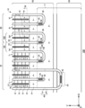
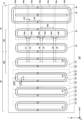
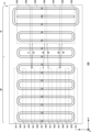
- FIG. 1 shows an example of a top view of a semiconductor device 100.
- FIG. A close-up view of an edge of an active region 110 in a top view of the semiconductor device 100 is shown.
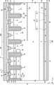
- 1B shows an example of a cross section taken along line aa' in FIG. 1B shows a modified example of the aa' cross section of FIG. 1B shows a modified example of the aa' cross section of FIG. 1 shows an example of a top view of a semiconductor device 100.
- FIG. 1 shows a modified example of the top view of the semiconductor device 100.
- 1 shows a modified example of the top view of the semiconductor device 100.
- 1 shows a modified example of the top view of the semiconductor device 100.
- 1 shows a modified example of the top view of the semiconductor device 100.
- 1 shows a modified example of the top view of the semiconductor device 100.
- FIG. 1 shows a modified example of the top view of the semiconductor device 100.
- 1 shows a modified example of the top view of the semiconductor device 100.
- 1 shows an example of a top view of a semiconductor device 500 of a comparative example.
- 1 shows an example of a top view of a semiconductor device 200.
- FIG. 1 shows an example of a top view of a semiconductor device 200.
- top one side in a direction parallel to the depth direction of the semiconductor substrate is referred to as "top” and the other side as “bottom.”
- bottom one side in a direction parallel to the depth direction of the semiconductor substrate
- top surface one surface is referred to as the top surface and the other surface is referred to as the bottom surface.
- the directions of "top,” “bottom,” “front,” and “back” are not limited to the direction of gravity or the direction in which the semiconductor device is attached to a substrate or the like when mounted.
- the plane parallel to the top surface of the semiconductor substrate is referred to as the XY plane, and the orthogonal axes parallel to the top and bottom surfaces of the semiconductor substrate are referred to as the X-axis and Y-axis.
- the axis perpendicular to the top and bottom surfaces of the semiconductor substrate is referred to as the Z-axis.
- the depth direction of the semiconductor substrate may be referred to as the Z-axis.
- the case where the semiconductor substrate is viewed in the Z-axis direction is referred to as a planar view.
- the direction parallel to the top and bottom surfaces of the semiconductor substrate, including the X-axis and Y-axis may be referred to as the horizontal direction.
- the first conductivity type is N type and the second conductivity type is P type, but the first conductivity type may be P type and the second conductivity type may be N type.
- the conductivity types of the substrate, layer, region, etc. in each embodiment will be of opposite polarity.
- the conductivity type of a doped region doped with impurities is described as P type or N type.
- impurities may specifically mean either N type donors or P type acceptors, and may be described as dopants.
- doping means introducing donors or acceptors into a semiconductor substrate to make it a semiconductor that exhibits N type conductivity or a semiconductor that exhibits P type conductivity.
- doping concentration refers to the donor concentration or acceptor concentration in thermal equilibrium.
- FIG. 1A shows an example of a top view of a semiconductor device 100.
- the semiconductor device 100 is a semiconductor chip that includes a transistor portion 70 and a diode portion 80.
- the transistor section 70 includes a transistor such as an IGBT (Insulated Gate Bipolar Transistor).
- the diode section 80 includes a diode such as a free wheel diode (FWD).
- the semiconductor device 100 of this example is a reverse conducting IGBT (RC-IGBT) that has the transistor section 70 and the diode section 80 on the same chip.
- RC-IGBT reverse conducting IGBT
- the semiconductor substrate 10 may be a silicon substrate, a silicon carbide substrate, a nitride semiconductor substrate such as gallium nitride, or the like.
- the semiconductor substrate 10 is a silicon substrate.
- the semiconductor substrate 10 has an active region 110 and a peripheral region 120.
- the transistor section 70 is a region obtained by projecting a collector region 22 (described later) provided on the underside of the semiconductor substrate 10 onto the upper surface of the semiconductor substrate 10.
- the diode section 80 is a region obtained by projecting a backside region 82 (described later) provided on the underside of the semiconductor substrate 10 onto the upper surface of the semiconductor substrate 10.
- the transistor sections 70 and diode sections 80 may be arranged alternately and periodically in the XY plane.
- the transistor sections 70 and diode sections 80 each include a plurality of transistor sections and diode sections.
- a gate metal layer 50 may be provided above the semiconductor substrate 10 in the region between the transistor sections 70 and the diode sections 80.
- the transistor section 70 and the diode section 80 have trench sections that extend in the Y-axis direction.
- the transistor section 70 and the diode section 80 may also have trench sections that extend in the X-axis direction.
- the active region 110 has a transistor portion 70 and a diode portion 80.
- the active region 110 is a region where a main current flows between the upper and lower surfaces of the semiconductor substrate 10 when the semiconductor device 100 is controlled to be in the on state. In other words, it is a region where a current flows in the depth direction inside the semiconductor substrate 10 from the upper surface to the lower surface, or from the lower surface to the upper surface.
- the transistor portion 70 and the diode portion 80 are referred to as the element portion or element region, respectively.
- the region sandwiched between the two element parts is also considered to be the active region 110.
- the region in which the gate metal layer 50 is provided and sandwiched between the element parts is also included in the active region 110.
- the gate metal layer 50 is formed of a material containing metal.
- the gate metal layer 50 is formed of aluminum, an aluminum-silicon alloy, or an aluminum-silicon-copper alloy.
- the gate metal layer 50 is electrically connected to the gate conductive portion of the transistor portion 70 and supplies a gate voltage to the transistor portion 70.
- the gate metal layer 50 is provided so as to surround the outer periphery of the active region 110 in a top view.
- the gate metal layer 50 is electrically connected to the gate pad 130 provided in the outer periphery region 120.
- the gate metal layer 50 may be provided along the outer periphery edge of the semiconductor substrate 10.
- the gate metal layer 50 may have a barrier metal formed of titanium, a titanium compound, or the like under a region formed of aluminum or the like.
- the gate metal layer 50 may also be provided between the transistor portion 70 and the diode portion 80 in a top view.
- the peripheral region 120 is a region between the active region 110 and the peripheral edge of the semiconductor substrate 10 when viewed from above.
- the peripheral region 120 is provided to surround the active region 110 when viewed from above.
- One or more metal pads may be arranged in the peripheral region 120 for connecting the semiconductor device 100 to an external device with a wire or the like.
- the peripheral region 120 may have an edge termination structure.
- the edge termination structure relieves electric field concentration on the upper surface side of the semiconductor substrate 10.
- the edge termination structure has a guard ring, a field plate, a resurf, or a structure that combines these.
- the gate pad 130 is electrically connected to the gate conductive portion of the transistor portion 70 via the gate metal layer 50.
- the gate pad 130 is set to the gate potential.
- the gate pad 130 is rectangular in top view.
- FIG. 1B shows an example of a top view of the semiconductor device 100. In this example, an enlarged view of area A in FIG. 1A is shown.
- the semiconductor device 100 of this example includes a gate trench portion 40, a dummy trench portion 30, an anode region 11, an emitter region 12, a base region 14, a first contact region 15, a well region 17, and a second contact region 19 on the front surface 21 of the semiconductor substrate 10.
- the front surface 21 will be described later.
- the semiconductor device 100 of this example also includes an emitter electrode 52 and a gate metal layer 50 provided above the front surface 21 of the semiconductor substrate 10.
- the emitter electrode 52 is provided above the gate trench portion 40, the dummy trench portion 30, the anode region 11, the emitter region 12, the base region 14, the first contact region 15, the well region 17, and the second contact region 19.
- the gate metal layer 50 is provided above the gate trench portion 40 and the well region 17.
- the emitter electrode 52 is formed of a material containing metal.
- the emitter electrode 52 may be formed of the same material as the gate metal layer, or may be formed of a different material.
- the emitter electrode 52 may have a barrier metal formed of titanium, a titanium compound, or the like, below a region formed of aluminum or the like.
- the emitter electrode 52 and the gate metal layer 50 are provided separately from each other.
- the emitter electrode 52 and the gate metal layer 50 are provided above the semiconductor substrate 10 with the interlayer insulating film 38 in between.
- the interlayer insulating film 38 is omitted in FIG. 1B.
- the interlayer insulating film 38 has contact holes 54, 55, and 56 penetrating therethrough.
- the contact hole 55 connects the gate metal layer 50 to the gate conductive portion in the transistor portion 70.
- a plug made of tungsten or the like may be formed inside the contact hole 55.
- the contact hole 56 connects the emitter electrode 52 to the dummy conductive portion in the dummy trench portion 30.
- a plug made of tungsten or the like may be formed inside the contact hole 56.
- connection portion 25 electrically connects the front surface electrode, such as the emitter electrode 52 or the gate metal layer 50, to the semiconductor substrate 10.
- the connection portion 25 is provided between the gate metal layer 50 and the gate conductive portion.
- the connection portion 25 is also provided between the emitter electrode 52 and the dummy conductive portion.
- the connection portion 25 is a conductive material, such as polysilicon doped with impurities.
- the connection portion 25 is polysilicon (N+) doped with N-type impurities.
- the connection portion 25 is provided above the front surface 21 of the semiconductor substrate 10 via an insulating film, such as an oxide film.
- the gate trench portion 40 is an example of a plurality of trench portions extending in a predetermined trench extension direction on the front surface 21 side of the semiconductor substrate 10.
- the gate trench portions 40 are arranged at predetermined intervals along a predetermined arrangement direction (the X-axis direction in this example).
- the gate trench portion 40 in this example may have two extension portions 41 extending parallel to the front surface 21 of the semiconductor substrate 10 and along an extension direction perpendicular to the arrangement direction (the Y-axis direction in this example), and a connection portion 43 connecting the two extension portions 41.
- connection portion 43 is formed in a curved shape.
- the gate metal layer 50 may be connected to the gate conductive portion.
- the dummy trench portion 30 is a trench portion electrically connected to the emitter electrode 52. Like the gate trench portion 40, the dummy trench portion 30 is arranged at predetermined intervals along a predetermined arrangement direction (the X-axis direction in this example). Like the gate trench portion 40, the dummy trench portion 30 in this example may have a U-shape on the front surface 21 of the semiconductor substrate 10. That is, the dummy trench portion 30 may have two extension portions 31 extending along the extension direction and a connection portion 33 connecting the two extension portions 31.
- the transistor section 70 in this example has a structure in which two gate trench sections 40 and three dummy trench sections 30 are repeatedly arranged. That is, the transistor section 70 in this example has gate trench sections 40 and dummy trench sections 30 in a ratio of 2:3. For example, the transistor section 70 has one extension section 31 between two extension sections 41. The transistor section 70 also has two extension sections 31 adjacent to the gate trench section 40.
- the ratio of the gate trench portion 40 to the dummy trench portion 30 is not limited to this example.
- the ratio of the gate trench portion 40 to the dummy trench portion 30 may be 1:1 or 2:4.
- the transistor portion 70 may have no dummy trench portion 30 and may be entirely made up of gate trench portions 40, forming a so-called full gate structure.
- the contact holes 54 are formed above the emitter region 12, the base region 14, and the first contact region 15.
- the contact holes 54 are provided above the anode region 11 and the second contact region 19.
- the contact holes 54 are provided above the base region 14. None of the contact holes 54 are provided above the well regions 17 provided at both ends in the Y-axis direction. In this way, one or more contact holes 54 are formed in the interlayer insulating film. The one or more contact holes 54 may be provided extending in the extension direction.
- the trench contact portion 27 electrically connects the emitter electrode 52 and the semiconductor substrate 10.
- the trench contact portion 27 is provided in the contact hole 54.
- the trench contact portion 27 is provided extending in the extension direction.
- the first boundary 190 is a region provided in the transistor portion 70 and adjacent to the diode portion 80.
- the first boundary 190 may have a base region 14.
- the first boundary 190 may have neither an emitter region 12 nor a first contact region 15.
- the trench portion of the first boundary 190 is a dummy trench portion 30.
- the first boundary 190 in this example is arranged so that both ends in the X-axis direction are dummy trench portions 30.
- the second boundary portion 290 is a region provided in the diode portion 80 and adjacent to the transistor portion 70.
- the second boundary portion 290 has an anode region 11.
- the second boundary portion 290 does not have a second contact region 19.
- the trench portion of the second boundary portion 290 is a dummy trench portion 30.
- the second boundary portion 290 is arranged so that both ends in the X-axis direction are dummy trench portions 30.
- Mesa portion 71, mesa portion 81, mesa portion 191, and mesa portion 291 are mesa portions provided adjacent to trench portions in a plane parallel to front surface 21 of semiconductor substrate 10.
- a mesa portion is a portion of semiconductor substrate 10 sandwiched between two adjacent trench portions, and may be a portion from front surface 21 of semiconductor substrate 10 to the deepest bottom of each trench portion.
- the extension portion of each trench portion may be considered as one trench portion. In other words, the area sandwiched between two extension portions may be considered as a mesa portion.
- the mesa portion 71 is provided in the transistor portion 70 adjacent to at least one of the dummy trench portion 30 or the gate trench portion 40.
- the mesa portion 71 has a well region 17, an emitter region 12, a base region 14, and a first contact region 15 on the front surface 21 of the semiconductor substrate 10.
- the emitter regions 12 and the first contact regions 15 are provided alternately in the extension direction.
- the mesa portion 81 is provided in a region of the diode portion 80 that is sandwiched between adjacent dummy trench portions 30.
- the mesa portion 81 has a second contact region 19 on the front surface 21 of the semiconductor substrate 10.
- the mesa portion 81 has a base region 14 and a well region 17 on the negative side in the Y-axis direction.
- the mesa portion 191 is provided in the first boundary portion 190.
- the mesa portion 191 has a base region 14 on the front surface 21 of the semiconductor substrate 10.
- the mesa portion 191 has a base region 14 and a well region 17 on the negative side in the Y-axis direction.
- the mesa portion 291 is provided in the second boundary portion 290.
- the mesa portion 291 has an anode region 11 on the front surface 21 of the semiconductor substrate 10.
- the mesa portion 291 has a base region 14 and a well region 17 on the negative side in the Y-axis direction.
- the anode region 11 is a region of a second conductivity type provided on the front surface 21 side of the semiconductor substrate 10 in the diode section 80.
- the anode region 11 is, for example, a P-type.
- the anode region 11 may be formed with the same dopant as the base region 14, or may be formed with a different dopant.
- the doping concentration of the anode region 11 may be the same as the doping concentration of the base region 14, or may be different.
- the base region 14 is a second conductivity type region provided on the front surface 21 side of the semiconductor substrate 10 in the transistor portion 70 and the diode portion 80.
- the base region 14 is P-type, for example.
- the base region 14 may be provided on both ends in the Y-axis direction of the mesa portion 71, the mesa portion 81, the mesa portion 191, and the mesa portion 291 on the front surface 21 of the semiconductor substrate 10. Note that FIG. 1B shows only one end of the base region 14 in the Y-axis direction.
- the emitter region 12 is a region of the first conductivity type having a higher doping concentration than the drift region 18.
- the emitter region 12 is, for example, N+ type.
- One example of a dopant for the emitter region 12 is arsenic (As).
- the emitter region 12 is provided in contact with the gate trench portion 40 on the front surface 21 of the mesa portion 71.
- the emitter region 12 may be provided extending in the X-axis direction from one of the two trench portions sandwiching the mesa portion 71 to the other.
- the emitter region 12 is also provided below the contact hole 54.
- the first contact region 15 is a region of a second conductivity type having a higher doping concentration than the base region 14.
- the first contact region 15 is a P+ type, for example.
- the first contact region 15 is provided on the front surface 21 of the mesa portion 71.
- the first contact region 15 may be provided in the X-axis direction from one of the two trench portions sandwiching the mesa portion 71 to the other.
- the first contact region 15 may or may not be in contact with the gate trench portion 40.
- the first contact region 15 may or may not be in contact with the dummy trench portion 30.
- the first contact region 15 is in contact with the dummy trench portion 30 and the gate trench portion 40.
- the first contact region 15 may also be provided below the contact hole 54.
- the second contact region 19 is a region of a second conductivity type having a higher doping concentration than the anode region 11.
- the second contact region 19 is P-type, for example.
- the doping concentration of the second contact region 19 may be the same as or different from the doping concentration of the first contact region 15.
- the doping concentration of the second contact region 19 in this example is lower than the doping concentration of the first contact region 15.
- the second contact region 19 in this example is provided on the front surface 21 of the mesa portion 81.
- the second contact region 19 may be provided in the X-axis direction from one of the two trench portions sandwiching the mesa portion 81 to the other.
- the second contact region 19 may or may not be in contact with the dummy trench portion 30.
- the second contact region 19 is in contact with the dummy trench portion 30.
- the second contact region 19 may also be provided below the contact hole 54.
- FIG. 1C is a diagram showing an example of the a-a' cross section in FIG. 1B.
- the a-a' cross section is an XZ plane passing through the emitter region 12 in the transistor section 70.
- the semiconductor device 100 of this example has a semiconductor substrate 10 including an accumulation region 16 and a trench bottom region 65, an interlayer insulating film 38, an emitter electrode 52, and a collector electrode 24.
- the emitter electrode 52 is formed above the semiconductor substrate 10 and the interlayer insulating film 38.
- the drift region 18 is a region of a first conductivity type provided in the semiconductor substrate 10.
- the drift region 18 is, as an example, N-type.
- the drift region 18 may be a region remaining in the semiconductor substrate 10 without other doped regions being formed therein.
- the doping concentration of the drift region 18 may be the doping concentration of the semiconductor substrate 10.
- the buffer region 20 is a region of a first conductivity type provided below the drift region 18.
- the buffer region 20 is, as an example, an N-type.
- the doping concentration of the buffer region 20 is higher than the doping concentration of the drift region 18.
- the buffer region 20 may function as a field stop layer that prevents the depletion layer spreading from the lower surface side of the base region 14 from reaching the collector region 22 of the second conductivity type and the back side region 82 of the first conductivity type.
- the collector region 22 is provided below the drift region 18 in the transistor portion 70.
- the collector region 22 has the second conductivity type.
- the collector region 22 is a P+ type.
- the back side region 82 is provided below the drift region 18 in the diode section 80.
- the back side region 82 has a first conductivity type section 82-1 and a second conductivity type section 82-2.
- the boundary between the collector region 22 and the back side region 82 is the boundary between the transistor section 70 and the diode section 80.
- the first conductivity type portion 82-1 is a region of the first conductivity type having a higher doping concentration than the drift region 18.
- the first conductivity type portion 82-1 of this example is provided in contact with the rear surface 23 of the semiconductor substrate 10.
- the doping concentration of the first conductivity type portion 82-1 may be higher than the doping concentration of the buffer region 20.
- the doping concentration of the first conductivity type portion 82-1 may be 1E15 cm -3 or more and 1E21 cm -3 or less.
- the first conductivity type portion 82-1 is N+ type.
- the second conductivity type portion 82-2 is a region of the second conductivity type having a higher doping concentration than the base region 14.
- the doping concentration of the second conductivity type portion 82-2 may be 1E16 cm -3 or more and 1E21 cm -3 or less.
- the second conductivity type portion 82-2 is P+ type.
- the doping concentration of the second conductivity type portion 82-2 may be the same as or different from the doping concentration of the collector region 22.
- the second conductivity type portion 82-2 of this example is in contact with the rear surface 23 of the semiconductor substrate 10 and is provided adjacent to the first conductivity type portion 82-1.
- the second conductivity type portion 82-2 may be in direct contact with the first conductivity type portion 82-1.
- the first conductivity type section 82-1 may be formed by ion implanting a P-type dopant and then further injecting an N-type dopant in the ion implantation process for forming the second conductivity type section 82-2.
- the second conductivity type section 82-2 may be formed by ion implanting an N-type dopant and then further injecting a P-type dopant in the ion implantation process for forming the first conductivity type section 82-1.
- the first conductivity type portion 82-1 and the second conductivity type portion 82-2 are provided to form a repeating structure in which the second conductivity type non-forming region 181 and the second conductivity type forming region 182 are alternately and repeatedly arranged in a predetermined direction.
- the second conductivity type non-forming region 181 is a region in which the second conductivity type portion 82-2 is not formed on the rear surface 23 side of the semiconductor substrate 10 when viewed from above.
- the second conductivity type forming region 182 is a region in which the second conductivity type portion 82-2 is formed on the rear surface 23 side of the semiconductor substrate 10 when viewed from above.
- the second-conductivity-type non-forming regions 181 and the second-conductivity-type forming regions 182 may be arranged alternately in the trench arrangement direction (e.g., the X-axis direction) or alternately in the trench extension direction (e.g., the Y-axis direction).
- the second-conductivity-type non-forming regions 181 and the second-conductivity-type forming regions 182 may be arranged in a striped pattern when viewed from above. This makes it possible to reduce the forward voltage Vf of the diode section 80.
- the arrangement of the second-conductivity-type non-forming regions 181 and the second-conductivity-type forming regions 182 will be described in detail later.
- the rear surface 23 of the semiconductor substrate 10 has a first conductivity type portion 82-1.
- the current during switching of the semiconductor device 100 is made uniform, improving the switching efficiency.
- the collector electrode 24 is formed on the rear surface 23 of the semiconductor substrate 10.
- the collector electrode 24 is formed of a conductive material such as a metal.
- the material of the collector electrode 24 may be the same as or different from the material of the emitter electrode 52 and the gate metal layer 50.
- the accumulation region 16 is a region of a first conductivity type that is provided closer to the front surface 21 of the semiconductor substrate 10 than the drift region 18.
- the accumulation region 16 is an N+ type, for example.
- the accumulation region 16 is provided in the transistor section 70. However, the accumulation region 16 does not necessarily have to be provided.
- the accumulation region 16 is provided in contact with the gate trench portion 40.
- the accumulation region 16 may or may not be in contact with the dummy trench portion 30.
- the doping concentration of the accumulation region 16 is higher than the doping concentration of the drift region 18.
- the interlayer insulating film 38 is provided on the front surface 21.
- An emitter electrode 52 is provided above the interlayer insulating film 38.
- One or more contact holes 54 are provided in the interlayer insulating film 38 to electrically connect the emitter electrode 52 to the semiconductor substrate 10.
- Contact holes 55 and 56 may also be provided penetrating the interlayer insulating film 38.
- the trench contact portion 27 has a conductive material filled in the contact hole 54.
- the trench contact portion 27 is provided between two adjacent trench portions among the multiple trench portions.
- the trench contact portion 27 is provided penetrating the emitter region 12 from the front surface 21.
- the trench contact portion 27 may have the same material as the emitter electrode 52.
- the bottom end of the trench contact portion 27 is deeper than the bottom end of the emitter region 12.
- the resistance of the base region 14 is reduced, making it easier to extract minority carriers (e.g., holes). This improves the breakdown resistance, such as the latch-up resistance, caused by minority carriers.
- the trench contact portion 27 has a bottom surface that is substantially planar.
- the bottom surface of the trench contact portion 27 may be covered with a plug layer of the second conductivity type or the like.
- the trench contact portion 27 has a tapered shape with inclined sidewalls.
- the sidewalls of the trench contact portion 27 may be provided substantially perpendicular to the front surface 21.
- One or more gate trench portions 40 and one or more dummy trench portions 30 are provided on the front surface 21.
- Each trench portion is provided from the front surface 21 to the drift region 18.
- each trench portion also penetrates these regions to reach the drift region 18.
- the trench portion penetrating the doping region is not limited to being manufactured in the order of forming the doping region and then the trench portion.
- the trench portion penetrating the doping region also includes a trench portion formed after the trench portion is formed.
- the gate trench portion 40 has a gate trench, a gate insulating film 42, and a gate conductive portion 44 formed on the front surface 21.
- the gate insulating film 42 is formed to cover the inner wall of the gate trench.
- the gate insulating film 42 may be formed by oxidizing or nitriding the semiconductor on the inner wall of the gate trench.
- the gate conductive portion 44 is formed inside the gate trench, further inside than the gate insulating film 42.
- the gate insulating film 42 insulates the gate conductive portion 44 from the semiconductor substrate 10.
- the gate conductive portion 44 is formed of a conductive material such as polysilicon.
- the gate trench portion 40 is covered by an interlayer insulating film 38 on the front surface 21.
- the gate conductive portion 44 includes a region facing the adjacent base region 14 on the mesa portion 71 side across the gate insulating film 42 in the depth direction of the semiconductor substrate 10. When a predetermined voltage is applied to the gate conductive portion 44, a channel is formed by an electron inversion layer on the surface layer of the interface of the base region 14 that contacts the gate trench.
- the dummy trench portion 30 may have the same structure as the gate trench portion 40.
- the dummy trench portion 30 has a dummy trench, a dummy insulating film 32, and a dummy conductive portion 34 formed on the front surface 21 side.
- the dummy insulating film 32 is formed to cover the inner wall of the dummy trench.
- the dummy conductive portion 34 is formed inside the dummy trench and is formed further inward than the dummy insulating film 32.
- the dummy insulating film 32 insulates the dummy conductive portion 34 from the semiconductor substrate 10.
- the dummy trench portion 30 is covered by an interlayer insulating film 38 on the front surface 21.
- the trench bottom region 65 is a region of a second conductivity type provided below the base region 14.
- the doping concentration of the trench bottom region 65 in this example is higher than the doping concentration of the base region 14.
- the trench bottom region 65 in this example is, for example, a P+ type.
- the doping concentration of the trench bottom region 65 may be 1E14 cm ⁇ 3 or more and 1E18 cm ⁇ 3 or less.
- the trench bottom region 65 in this example is provided so that its upper end does not contact the accumulation region 16. That is, in the depth direction of the semiconductor substrate 10, the drift region 18 is formed between the trench bottom region 65 and the accumulation region 16.
- the trench bottom region 65 may be provided so that its upper end contacts the lower end of the accumulation region 16.
- the trench bottom region 65 in this example is provided so as to extend from the lower end of one of the multiple trench portions to the lower end of the other opposing trench portion in the trench arrangement direction of the multiple trench portions.
- the trench bottom region 65 may be provided so as to extend from the lower end of one of the multiple trench portions beyond the lower end of the other opposing trench portion to the lower end of the trench portion adjacent to the other opposing trench portion.
- the trench bottom region 65 may be provided so as to extend beyond the lower ends of two or more multiple trench portions.
- the first lifetime control region 151 is provided in the diode section 80. This allows the semiconductor device 100 of this example to speed up recovery in the diode section 80 and reduce switching losses.
- the first lifetime control region 151 may also be provided in the transistor section 70.
- the first lifetime control region 151 may be formed by injecting impurities from the front surface 21 side, or from the back surface 23 side.
- the first lifetime control region 151 may be formed by ion implantation of helium into the semiconductor substrate 10.
- the second lifetime control region 152 is provided on the front surface 21 side of the center of the semiconductor substrate 10 in the depth direction of the semiconductor substrate 10.
- the second lifetime control region 152 is provided in the drift region 18.
- the second lifetime control region 152 is provided in both the transistor section 70 and the diode section 80.
- the second lifetime control region 152 may be formed by injecting impurities from the front surface 21 side, or may be formed by injecting impurities from the back surface 23 side.
- the second lifetime control region 152 is provided in the diode section 80, the first boundary section 190, and the second boundary section 290, and may not be provided in a part of the transistor section 70.
- the second lifetime control region 152 may be formed by any of the methods for forming the first lifetime control region 151.
- the elements and dose amounts used to form the first lifetime control region 151 and the second lifetime control region 152 may be the same or different.
- FIG. 1D is a diagram showing a modified example of the a-a' cross section in FIG. 1B. The differences from FIG. 1C will be explained using FIG. 1D.
- the first conductivity type portion 82-1 is provided on the rear surface 23 of the semiconductor substrate 10.
- the first conductivity type portion 82-1 may function as the cathode of the diode portion 80.
- the second conductivity type section 82-2 is provided above the first conductivity type section 82-1.
- the second conductivity type section 82-2 is provided in contact with the first conductivity type section 82-1, but this is not limited to this.
- the second conductivity type section 82-2 may be provided spaced apart from the first conductivity type section 82-1.
- the second conductivity type portion 82-2 has the same thickness as the first conductivity type portion 82-1.
- the second conductivity type portion 82-2 may be thinner than the first conductivity type portion 82-1.
- the second conductivity type portion 82-2 may have a thickness equal to or less than the length from the upper end of the first conductivity type portion 82-1 to the lower end of the first lifetime control region 151.
- the second conductivity type portion 82-2 in this example is provided closer to the back surface 23 of the semiconductor substrate 10 than the first lifetime control region 151.
- the second conductivity type portion 82-2 may also be provided closer to the front surface 21 of the semiconductor substrate 10 than the first lifetime control region 151.
- the second-conductivity-type non-forming region 181 is a region in which the second-conductivity-type portion 82-2 is not formed on the rear surface 23 side of the semiconductor substrate 10 when viewed from above.
- the second-conductivity-type forming region 182 is a region in which the second-conductivity-type portion 82-2 is formed on the rear surface 23 side of the semiconductor substrate 10 when viewed from above. Even when the second-conductivity-type portion 82-2 is formed above the first-conductivity-type portion 82-1 as in this example, a repeating structure can be formed in which the second-conductivity-type non-forming region 181 and the second-conductivity-type forming region 182 are alternately and repeatedly arranged when viewed from above.
- FIG. 1E is a diagram showing a modified example of the a-a' cross section in FIG. 1B. The differences from FIG. 1C will be explained using FIG. 1E.
- the depth position of the lower end of the trench bottom region 65 is located closer to the front surface 21 than the depth positions of the trench bottoms of the multiple trench portions.
- the depth position of the upper end of the trench bottom region 65 is located deeper than the base region 14.
- the depth position of the upper end of the trench bottom region 65 may be located deeper than the accumulation region 16.
- a drift region 18 may be provided between the trench bottom region 65 and the accumulation region 16.
- the trench bottom region 65 is provided such that the depth position of the bottom end is shallower than the depth positions of the bottom ends of the gate trench portion 40 and the dummy trench portion 30. In other words, the trench bottom region 65 does not need to cover the trench bottoms of the gate trench portion 40 and the dummy trench portion 30. Even in such a case, it is possible to increase the gate capacitance of the transistor portion 70 and reduce the on-loss Eon of the semiconductor device 100.
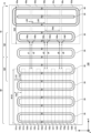
- FIG. 2A shows an example of a top view of the semiconductor device 100.
- the positional relationship between the trench bottom region 65, the second conductivity type non-forming region 181, and the second conductivity type forming region 182 in the semiconductor device 100 of this example will be explained.
- the configuration necessary for explanation is shown, and other configurations are omitted.
- the transistor section 70 has a plurality of trench bottom regions 65 repeatedly arranged in the trench extension direction of the plurality of trench sections (the Y-axis direction in this example).
- the transistor section 70 has a plurality of trench bottomless regions 66 repeatedly arranged in the trench extension direction and sandwiched between the plurality of trench bottom regions 65.
- the trench bottom regions 65 and the trench bottomless regions 66 extend from the transistor section 70 toward the diode section 80 in the trench arrangement direction, but do not reach the diode section 80 and terminate at the first boundary section 190.
- the width W65 of the trench bottom region 65 in the trench arrangement direction may be the same as the width of the transistor section 70 in the trench arrangement direction, or may be smaller than the width of the transistor section 70 in the trench arrangement direction.
- the trench bottom region 65 may be provided extending from one end to the other end of the transistor section 70 in the trench arrangement direction.
- the multiple trench bottom regions 65 are repeatedly arranged at a predetermined trench bottom repetition period P65.
- the trench bottom repetition period P65 may be the distance from one end of one trench bottom region 65 in the trench extension direction, beyond the other end of the trench bottom region, to an adjacent trench bottom region 65.
- the trench bottom repetition period P65 is the distance from the Y-axis negative end edge of trench bottom region 65b to the Y-axis negative end edge of trench bottom region 65c.
- the trench bottom repeat period P65 is greater than the back side repeat period P82 described below.
- the trench bottom repeat period P65 may be an integer multiple of the back side repeat period P82.
- the trench bottom repeat period P65 is 5 ⁇ m or more and 200 ⁇ m or less.
- the area of the trench bottom region 65 is larger than the area of the trench bottomless region 66.
- the width L65 of the trench bottom region 65 in the trench extension direction is larger than the width L66 of the trench bottomless region 66 in the trench extension direction.
- the width L65 of the trench bottom region 65 in the trench extension direction is 1 to 10 times the width L66 of the trench bottomless region 66.
- the width L65 of the trench bottom region 65 in the trench extension direction may be larger than the width L181 of the second conductivity type non-forming region 181 in the trench extension direction, and may be larger than the width L182 of the second conductivity type forming region 182 in the trench extension direction.
- the areas of the multiple trench bottomless regions 66 sandwiched between the multiple trench bottom regions 65 may be approximately the same. In one example, the areas of the multiple trench bottomless regions 66 sandwiched between the multiple trench bottom regions 65 are each 85% or more and 115% or less of a predetermined reference value. As one example, the area of the trench bottomless region 66a in a top view is the same as the area of the trench bottomless region 66b.
- the predetermined reference value may be the area of any one of the areas of the multiple trench bottomless regions 66.
- the predetermined reference value may be the average value, the minimum value, or the maximum value of the areas of the multiple trench bottomless regions 66.
- the diode section 80 is provided with a second-conductivity-type non-forming region 181 and a second-conductivity-type forming region 182.
- the second-conductivity-type non-forming region 181 and the second-conductivity-type forming region 182 extend in the trench arrangement direction (the X-axis direction in this example) and are arranged alternately in the trench extension direction.
- the second-conductivity-type non-forming region 181 and the second-conductivity-type forming region 182 extend from the diode section 80 toward the transistor section 70 in the trench arrangement direction, but do not reach the transistor section 70 and terminate at the second boundary section 290.
- the width W181 of the second-conductivity-type non-forming region 181 in the trench arrangement direction may be the same as the width of the diode section 80 in the trench arrangement direction, or may be smaller than the width of the diode section 80 in the trench arrangement direction.
- the second-conductivity-type non-forming region 181 may be provided extending from one end to the other end of the diode section 80 in the trench arrangement direction.
- the second-conductivity-type non-forming regions 181 and the second-conductivity-type forming regions 182 are alternately arranged at a predetermined back-side repetition period P82.
- the back-side repetition period P82 may be the distance from one end of one second-conductivity-type non-forming region 181 in the trench extension direction, beyond the other end of the second-conductivity-type non-forming region 181, to the adjacent second-conductivity-type non-forming region 181.
- the back-side repetition period P82 is the distance from the end edge on the Y-axis positive side of the second-conductivity-type non-forming region 181a to the end edge on the Y-axis positive side of the second-conductivity-type non-forming region 181b.
- the back side repetition period P82 is smaller than the trench bottom repetition period P65.
- the back side repetition period P82 may be 20 ⁇ m, 30 ⁇ m, or 50 ⁇ m. In one example, the back side repetition period P82 is 10 ⁇ m or more and 100 ⁇ m or less.
- the second-conductivity-type non-forming regions 181 and the second-conductivity-type forming regions 182 may be arranged alternately in the trench extension direction, or may be arranged alternately in the trench arrangement direction.
- the second-conductivity-type non-forming regions 181 and the second-conductivity-type forming regions 182 extend in the trench arrangement direction and are arranged alternately in the trench extension direction.
- the area of the second conductivity type non-forming region 181 and the area of the second conductivity type forming region 182 are the same.
- the area of the second conductivity type non-forming region 181a and the area of the second conductivity type forming region 182a are the same.
- the areas of the second conductivity type non-forming region 181 and the second conductivity type forming region 182 may be different.
- the width L181 of the second conductivity type non-forming region 181 in the trench extension direction may be different from the width L182 of the second conductivity type forming region in the trench extension direction.
- the width L181 of the second conductivity type non-forming region 181 in the trench extension direction is 30% or more and 70% or less of the sum of the width L181 of the second conductivity type non-forming region 181 and the width L182 of the second conductivity type forming region 182 in the trench extension direction.
- the area of the second conductivity type non-forming region 181 may be 30% or more and 70% or less of the area of the back side region 82.
- each end 166 of the multiple trench bottomless regions 66 is 85% or more and 115% or less of a predetermined reference value.
- each end 166 of the multiple trench bottomless regions 66 is a corner of the trench bottomless region 66.
- the predetermined reference value may be the shortest distance from any one of the multiple ends 166 to the second-conductivity-type non-forming region 181.
- the predetermined reference value may be the average value, minimum value, or maximum value of the shortest distances from each of the multiple ends 166 to the second-conductivity-type non-forming region 181.
- the shortest distance from the end 166a on the positive side of the Y axis of the trench bottomless region 66a to the second-conductivity-type non-forming region 181c is indicated as d1.
- d2 to d6 are the shortest distances from the end 166b of the trench bottomless region 66a, the end 166c and the end 166d of the trench bottomless region 66b, and the end 166e and the end 166f of the trench bottomless region 66c to the second-conductivity-type non-forming region 181.
- the shortest distances d1 to d6 from the end 166 of each of the multiple trench bottomless regions 66 to the multiple second-conductivity-type non-forming regions 181 are all approximately the same.
- the distance from each end 166 of each trench bottomless region 66 to the second-conductivity-type non-forming region 181 is uniformed. This makes it possible to uniform the electronic current flowing when the semiconductor device 100 is switched on, thereby reducing the on-loss Eon.
- each of the multiple trench bottomless regions 66 faces one of the multiple second-conductivity-type non-forming regions 181.
- trench bottomless region 66a faces second-conductivity-type non-forming region 181c
- trench bottomless region 66b faces second-conductivity-type non-forming region 181e
- trench bottomless region 66c faces second-conductivity-type non-forming region 181g.
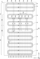
- FIG. 2B shows a modified top view of the semiconductor device 100. Differences from FIG. 2A will be explained using FIG. 2B.
- the trench bottom repeat period P65 is the same as in the example shown in FIG. 2A.
- the width L65 of the trench bottom region is smaller than in the example shown in FIG. 2A, and the width L66 of the trench bottomless region is larger than in the example shown in FIG. 2A.
- the area occupied by the trench bottomless region 66 in one trench bottom repeat period P65 is larger than in the example shown in FIG. 2A.
- the width L181 of the second-conductivity-type non-forming region 181 and the width L182 of the second-conductivity-type forming region 182 are smaller than those in the example shown in FIG. 2A.
- the back-surface-side repetition period P82 is smaller than that in the example shown in FIG. 2A.
- each of the multiple trench bottomless regions 66 faces two or more of the multiple second-conductivity-type non-forming regions 181 in the trench arrangement direction of the multiple trench portions.
- a total of three second-conductivity-type non-forming regions 181 are provided to face one trench bottomless region 66: one second-conductivity-type non-forming region 181 having the same center line as one trench bottomless region 66, and two second-conductivity-type non-forming regions 181 provided line-symmetrically on both sides of the center line of the second-conductivity-type non-forming region 181.
- the shortest distances d1 to d6 from the respective ends 166 of the multiple trench bottomless regions 66 to the second-conductivity-type non-forming regions 181 are all approximately the same. This allows the electron current from the trench bottomless region 66 to be uniformly distributed, thereby reducing the on-loss Eon of the semiconductor device 100.
- the number of second-conductivity-type non-forming regions 181 facing one trench bottomless region 66 is not limited to this example.
- One trench bottomless region 66 may face two second-conductivity-type non-forming regions 181, or may face four or more second-conductivity-type non-forming regions 181.
- FIG. 2C shows a modified top view of the semiconductor device 100. Differences from FIG. 2A will be explained using FIG. 2C.
- the second-conductivity-type non-forming region 181 in this example has a predetermined length L181x in the trench arrangement direction of the multiple trench portions (X direction in this example), and a predetermined width L181y in the trench extension direction of the multiple trench portions (Y direction in this example).
- the length L181x and the width L181y may be approximately the same, so that the second-conductivity-type non-forming region 181 may be provided in an approximately square shape when viewed from above.
- the length L181x and the width L181y may be different.
- the second-conductivity-type non-forming regions 181 and the second-conductivity-type forming regions 182 are arranged alternately and repeatedly in two directions.
- the second-conductivity-type non-forming regions 181 and the second-conductivity-type forming regions 182 may have an arrangement direction period P82x in the trench arrangement direction of the multiple trench portions (in this example, the X direction) and an extension direction period P82y in the trench extension direction of the multiple trench portions (in this example, the Y direction).
- the arrangement direction period P82x and the extension direction period P82y may be substantially the same, whereby the second-conductivity-type non-forming regions 181 and the second-conductivity-type forming regions 182 may be arranged in a dot shape in a top view. Even in such a case, the distance from each end 166 of each trench bottomless region 66 to the second-conductivity-type non-forming region 181 can be made uniform, thereby reducing the on-loss Eon.
- the arrangement direction period P82x and the extension direction period P82y may be different.
- FIG. 2D shows a modified top view of the semiconductor device 100.
- FIG. 2D is an example of a top view in which the depth positions of the lower ends of the multiple trench bottom regions 65 are located closer to the front surface 21 of the semiconductor substrate 10 than the depth positions of the trench bottoms of the multiple trench portions, as in FIG. 1E.
- the trench bottom regions 65 do not cover the trench bottoms of the trench portions. Therefore, in a top view, the trench bottom regions 65 are provided only in the mesa portion of the transistor portion 70.
- the electron current also flows through the trench bottomless region 66, so that the distance from each end 166 of each trench bottomless region 66 to the second conductivity type non-forming region 181 can be made uniform, as in the cases described in FIG. 2A to FIG. 2C, and the on-loss Eon can be reduced.
- FIG. 3A shows a modified top view of the semiconductor device 100.
- the trench bottom repeat period P65 and the back side repeat period P82 are the same as those in the example of FIG. 2A.
- the example of FIG. 3A differs from the example of FIG. 2A in that the trench bottomless region 66 faces the second conductivity type forming region 182 in the trench arrangement direction.
- each of the multiple trench bottomless regions 66 may face one of the multiple second conductivity type forming regions 182. In other words, in the trench arrangement direction, each of the multiple trench bottomless regions 66 does not have to face one of the multiple second conductivity type non-forming regions 181.
- the trench bottomless region 66a faces the second conductivity type forming region 182a
- the trench bottomless region 66b faces the second conductivity type forming region 182c
- the trench bottomless region 66c faces the second conductivity type forming region 182e
- the trench bottomless region 66d faces the second conductivity type forming region 182g.
- the shortest distances d1 to d6 from the ends 166 of the trench bottomless regions 66 to the second-conductivity-type non-forming regions 181 are all substantially the same, as in the example shown in FIG. 2A. Therefore, the length of the path through which the electron current flows when the semiconductor device 100 is switched on can be made uniform in each trench bottomless region 66, thereby reducing the on-loss Eon.
- the distance W indicates the offset width between the end 166 of the trench bottomless region 66 in the trench extension direction and the second-conductivity-type non-forming region 181 in a top view.
- the end 166 does not face the second-conductivity-type non-forming region 181, so the distance W is greater than 0.
- the distance W may be greater than 0 and less than or equal to 50% of the width of the trench bottom region 65 in the trench extension direction.
- FIG. 3B shows a modified top view of the semiconductor device 100. Differences from FIG. 2B will be explained using FIG. 3B.
- each of the trench bottomless regions 66 may face two or more of the second conductivity type forming regions 182.
- a total of three second conductivity type forming regions 182 are provided to face one trench bottomless region 66, including one second conductivity type forming region 182 having the same center line as one trench bottomless region 66 and two second conductivity type forming regions 182 provided line-symmetrically on both sides of the second conductivity type forming region 182 across the center line.
- the shortest distances d1 to d6 from the respective ends 166 of the trench bottomless regions 66 to the second conductivity type non-forming region 181 are all approximately the same.
- the electron current from the trench bottomless region 66 is uniformly distributed, thereby reducing the on-loss Eon of the semiconductor device 100.
- FIG. 4 shows a modified top view of the semiconductor device 100. Differences from FIG. 2A will be explained using FIG. 4.
- the second-conductivity-type non-forming regions 181 and the second-conductivity-type forming regions 182 extend in the trench extension direction and are arranged alternately in the trench arrangement direction.
- the second-conductivity-type non-forming regions 181 are provided perpendicular to the arrangement direction of the multiple trench bottomless regions 66, so that the shortest distances d1 to d6 from the ends 166 of the multiple trench bottomless regions 66 to the second-conductivity-type non-forming regions 181 are all the same. This allows the electron current from the trench bottomless regions 66 to be uniformly distributed, thereby reducing the on-loss Eon of the semiconductor device 100.
- FIG. 5 shows an example of a top view of a semiconductor device 500 of the comparative example.
- the semiconductor device 500 of the comparative example has a plurality of trench bottom regions 565 repeatedly provided in the trench extension direction of a plurality of trench portions, and a plurality of trench bottomless regions 566 repeatedly provided in the trench extension direction and sandwiched between the plurality of trench bottom regions 565.
- the semiconductor device 500 of the comparative example has second-conductivity-type non-forming regions 581 and second-conductivity-type forming regions 582 extending in the trench arrangement direction and arranged alternately in the trench extension direction.
- the semiconductor device 500 of the comparative example there is no restriction between the position where the trench bottomless region 566 is provided and the position where the second-conductivity-type non-forming region 581 is provided.
- the second-conductivity-type non-forming region 581 and the second-conductivity-type forming region 582 are not provided in line symmetry with respect to the center line of one trench bottomless region 566.
- the semiconductor device 500 of the comparative example there is no restriction between the position where the trench bottomless region 566 is provided and the position where the second conductivity type non-forming region 581 is provided, so the shortest distance from the end of each trench bottomless region 566 to the second conductivity type non-forming region 581 varies for each trench bottomless region 566. That is, in the semiconductor device 500 of the comparative example, the shortest distances d1 to d6 are not approximately the same.
- the shortest distance from each end of the multiple trench bottomless regions to the second conductivity type non-forming region can be made uniform.
- the shortest distances d1 to d6 from each end of the multiple trench bottomless regions to the second conductivity type non-forming region can all be made approximately the same.
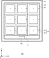
- FIG. 6A shows an example of a top view of the semiconductor device 200.
- the semiconductor device 200 is a semiconductor chip having a transistor portion 70 and a diode portion 80.
- the semiconductor device 200 differs from the semiconductor device 100 in the shapes of the transistor section 70 and the diode section 80.
- the diode section 80 is provided so as to surround the outer periphery of the transistor section 70.
- the semiconductor device 200 may include a plurality of unit structures in which the outer periphery of the transistor section 70 is surrounded by the diode section 80.
- the semiconductor device 200 includes a total of nine unit structures, with the unit structure being repeated three times in each of the X-axis direction and the Y-axis direction.
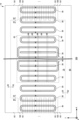
- FIG. 6B shows an example of a top view of the semiconductor device 200. In this example, an enlarged view of region B in FIG. 6A is shown.
- the transistor section 70 has multiple trench sections including the gate trench section 40 and the dummy trench section 30.
- the diode section 80 has multiple trench sections including the dummy trench section 30. Note that the diode section 80 does not necessarily have to have a trench section.
- the transistor section 70 has a plurality of trench bottom regions 65 repeatedly arranged in the trench extension direction of the plurality of trench sections (the Y-axis direction in this example).
- the transistor section 70 has a plurality of trench bottomless regions 66 repeatedly arranged in the trench extension direction and sandwiched between the plurality of trench bottom regions 65.
- the trench bottom regions 65 and the trench bottomless regions 66 extend from the transistor section 70 toward the diode section 80 in the trench arrangement direction, and terminate without reaching the diode section 80.
- the diode section 80 of this example has second-conductivity-type non-forming regions 181 and second-conductivity-type forming regions 182 that are alternately arranged in the trench extension direction of the multiple trench sections in a region facing the multiple trench bottomless regions 66. This makes it possible to equalize the electronic current that flows when the semiconductor device 200 is switched on, and reduce the on-loss Eon, even when the diode section 80 surrounds the outer periphery of the transistor section 70.
- the diode section 80 may not have a second-conductivity-type forming region 182 in a region that does not face the multiple trench bottomless regions 66.
- the second-conductivity-type forming region 182 is not provided in the diode section 80 adjacent to the transistor section 70 in the trench extension direction of the multiple trench sections.
- the trench bottom of the gate trench section 40 in the trench extension direction is covered with the trench bottom region 65, so that no electronic current flows. Therefore, in a region that does not face the multiple trench bottomless regions 66, the on-loss Eon of the semiconductor device 200 is not affected even if the second-conductivity-type non-forming region 181 and the second-conductivity-type forming region 182 are not arranged alternately.
- 10 semiconductor substrate, 11: anode region, 12: emitter region, 14: base region, 15: first contact region, 16: accumulation region, 17: well region, 18: drift region, 19: second contact region, 20: buffer region, 21: front surface, 22: collector region, 23: back surface, 24: collector electrode, 25: connection portion, 27: trench contact portion, 30: dummy trench portion, 31: extension portion, 32: dummy insulating film, 33: connection portion, 34: dummy conductive portion, 38: interlayer insulating film, 40: gate trench portion, 41: extension portion, 42: gate insulating film, 43: connection portion, 44: gate conductive portion, 50: gate metal layer, 52: emitter electrode, 54: contact hole, 55: contact hole, 56: contact hole 1.
Landscapes
- Metal-Oxide And Bipolar Metal-Oxide Semiconductor Integrated Circuits (AREA)
- Electrodes Of Semiconductors (AREA)
Abstract
トランジスタ部およびダイオード部を備える半導体装置であって、半導体基板に設けられた第1導電型のドリフト領域と、前記半導体基板のおもて面側において、予め定められたトレンチ延伸方向に延伸した複数のトレンチ部と、前記ドリフト領域の下方に設けられた第2導電型のコレクタ領域と、を備える、半導体装置を提供する。前記トランジスタ部は、前記ドリフト領域の上方に設けられた第2導電型のベース領域と、前記ドリフト領域よりもドーピング濃度が高い第1導電型のエミッタ領域と、前記ベース領域よりもドーピング濃度が高い第2導電型の第1コンタクト領域と、前記ベース領域の下方において、前記トレンチ延伸方向に繰り返し設けられた第2導電型の複数のトレンチボトム領域と、前記トレンチ延伸方向に繰り返し設けられ、前記複数のトレンチボトム領域に挟まれた複数のトレンチボトムレス領域とを有してよい。前記ダイオード部は、前記ドリフト領域の上方に設けられた第2導電型のアノード領域と、前記ドリフト領域の下方に設けられた裏面側領域とを有してよい。前記裏面側領域は、第1導電型の第1導電型部と、第2導電型の第2導電型部とを含んでよい。前記第1導電型部および前記第2導電型部は、上面視において、前記第2導電型部が形成された第2導電型形成領域と、前記第2導電型部が形成されていない第2導電型非形成領域とが予め定められた方向に交互に繰り返し配列された繰り返し構造を形成するように設けられてよい。上面視において、前記複数のトレンチボトムレス領域のそれぞれの端部から前記第2導電型非形成領域までの最短距離は、予め定められた基準値の85%以上、115%以下であってよい。
Description
本発明は、半導体装置に関する。
特許文献1には、「露出されたトレンチ14、15、16の底部の下方で、(第1の導電型と相補的な)第2の導電型の複数のドーピング領域(例えば、注入領域)1059が生成される」と記載されている。特許文献2には「幅の狭いFWD領域19a」および「幅の広いFWD領域19b」を設けることが記載されている。
[先行技術文献]
[特許文献]
[特許文献1] 特開2019-110288号公報
[特許文献2] 特許第5637175号公報
[先行技術文献]
[特許文献]
[特許文献1] 特開2019-110288号公報
[特許文献2] 特許第5637175号公報
(解決しようとする課題)
半導体装置の動作初期において、電子電流を均一化することが望ましい。
(課題を解決するための手段)
半導体装置の動作初期において、電子電流を均一化することが望ましい。
(課題を解決するための手段)
本発明の第1の態様においては、トランジスタ部およびダイオード部を備える半導体装置であって、半導体基板に設けられた第1導電型のドリフト領域と、前記半導体基板のおもて面側において、予め定められたトレンチ延伸方向に延伸した複数のトレンチ部と、前記ドリフト領域の下方に設けられた第2導電型のコレクタ領域と、を備える、半導体装置を提供する。前記トランジスタ部は、前記ドリフト領域の上方に設けられた第2導電型のベース領域と、前記ドリフト領域よりもドーピング濃度が高い第1導電型のエミッタ領域と、前記ベース領域よりもドーピング濃度が高い第2導電型の第1コンタクト領域と、前記ベース領域の下方において、前記トレンチ延伸方向に繰り返し設けられた第2導電型の複数のトレンチボトム領域と、前記トレンチ延伸方向に繰り返し設けられ、前記複数のトレンチボトム領域に挟まれた複数のトレンチボトムレス領域とを有してよい。前記ダイオード部は、前記ドリフト領域の上方に設けられた第2導電型のアノード領域と、前記ドリフト領域の下方に設けられた裏面側領域とを有してよい。前記裏面側領域は、第1導電型の第1導電型部と、第2導電型の第2導電型部とを含んでよい。前記第1導電型部および前記第2導電型部は、上面視において、前記第2導電型部が形成された第2導電型形成領域と、前記第2導電型部が形成されていない第2導電型非形成領域とが予め定められた方向に交互に繰り返し配列された繰り返し構造を形成するように設けられてよい。上面視において、前記複数のトレンチボトムレス領域のそれぞれの端部から前記第2導電型非形成領域までの最短距離は、予め定められた基準値の85%以上、115%以下であってよい。
上記半導体装置において、前記第2導電型非形成領域および前記第2導電型形成領域は、上面視において、前記トレンチ延伸方向に延伸し、前記複数のトレンチ部のトレンチ配列方向に交互に配置されてよい。
上記いずれかの半導体装置において、前記第2導電型非形成領域および前記第2導電型形成領域は、上面視において、前記複数のトレンチ部のトレンチ配列方向に延伸し、前記トレンチ延伸方向に交互に配置されてよい。
上記いずれかの半導体装置においては、上面視において、前記第2導電型非形成領域の面積は、前記裏面側領域の面積の30%以上、70%以下であってよい。
上記いずれかの半導体装置において、前記裏面側領域は、複数の前記第2導電型非形成領域を有してよい。前記複数のトレンチ部のトレンチ配列方向において、前記複数のトレンチボトムレス領域のそれぞれは、前記複数の第2導電型非形成領域のうちのいずれかと対向してよい。
上記いずれかの半導体装置において、前記裏面側領域は、複数の前記第2導電型非形成領域を有してよい。前記複数のトレンチ部のトレンチ配列方向において、前記複数のトレンチボトムレス領域のそれぞれは、前記複数の第2導電型非形成領域のうちの2つ以上と対向してよい。
上記いずれかの半導体装置において、前記裏面側領域は、複数の前記第2導電型形成領域を有してよい。前記複数のトレンチ部のトレンチ配列方向において、前記複数のトレンチボトムレス領域のそれぞれは、前記複数の第2導電型形成領域のうちのいずれかと対向してよい。
上記いずれかの半導体装置において、前記裏面側領域は、複数の前記第2導電型形成領域を有してよい。前記複数のトレンチ部のトレンチ配列方向において、前記複数のトレンチボトムレス領域のそれぞれは、前記複数の第2導電型形成領域のうちの2つ以上と対向してよい。
上記いずれかの半導体装置において、前記複数のトレンチボトム領域で挟まれた前記複数のトレンチボトムレス領域の面積は、それぞれ予め定められた基準値の85%以上、115%以下であってよい。
上記いずれかの半導体装置において、前記トランジスタ部は、前記ダイオード部と隣接して設けられ、前記ドリフト領域の上方に前記第1コンタクト領域が設けられない第1境界部を有してよい。前記ダイオード部は、前記ドリフト領域の上方に設けられ、前記アノード領域よりもドーピング濃度の高い第2導電型の第2コンタクト領域と、前記トランジスタ部と隣接して設けられ、前記第2コンタクト領域が設けられていない第2境界部とを有してよい。前記第2境界部において、前記半導体基板の裏面は、前記第1導電型部を有してよい。
上記いずれかの半導体装置において、前記第2導電型非形成領域および前記第2導電型形成領域は、前記トレンチ延伸方向における前記複数のトレンチボトムレス領域の1つのトレンチボトムレス領域の中心線を基準に線対称に設けられてよい。
上記いずれかの半導体装置において、前記第2導電型非形成領域および前記第2導電型形成領域は、予め定められた裏面側繰り返し周期で交互に配置されてよい。前記複数のトレンチボトム領域は、予め定められたトレンチボトム繰り返し周期で繰り返し配置されてよい。前記トレンチボトム繰り返し周期は、前記裏面側繰り返し周期よりも大きくてよい。
上記いずれかの半導体装置において、前記裏面側繰り返し周期は、10μm以上、100μm以下であってよい。
上記いずれかの半導体装置において、前記トレンチボトム繰り返し周期は、前記裏面側繰り返し周期の整数倍であってよい。
上記いずれかの半導体装置において、前記第1導電型部は、前記半導体基板の裏面に接して設けられてよい。前記第2導電型部は、前記半導体基板の裏面に接し、前記第1導電型部と隣接して設けられてよい。
上記いずれかの半導体装置において、前記第1導電型部は、前記半導体基板の裏面に接して設けられてよい。前記第2導電型部は、前記第1導電型部の上方に設けられてよい。
上記いずれかの半導体装置においては、前記半導体基板の深さ方向において、前記複数のトレンチボトム領域の下端の深さ位置は、前記複数のトレンチ部のトレンチ底部の深さ位置よりも前記おもて面側に設けられてよい。
なお、上記の発明の概要は、本発明の特徴の全てを列挙したものではない。また、これらの特徴群のサブコンビネーションもまた、発明となりうる。
以下、発明の実施の形態を通じて本発明を説明するが、以下の実施形態は請求の範囲にかかる発明を限定するものではない。また、実施形態の中で説明されている特徴の組み合わせの全てが発明の解決手段に必須であるとは限らない。
本明細書においては、半導体基板の深さ方向と平行な方向における一方の側を「上」、他方の側を「下」と称する。基板、層またはその他の部材の2つの主面のうち、一方の面を上面、他方の面を下面と称する。「上」、「下」、「おもて」、「裏」の方向は重力方向、または、半導体装置の実装時における基板等への取り付け方向に限定されない。
本明細書では、X軸、Y軸およびZ軸の直交座標軸を用いて技術的事項を説明する場合がある。直交座標軸は、構成要素の相対位置を特定するに過ぎず、特定の方向を限定するものではない。例えば、Z軸は地面に対する高さ方向を限定して示すものではない。なお、+Z軸方向と-Z軸方向とは互いに逆向きの方向である。正負を記載せず、Z軸方向と記載した場合、+Z軸および-Z軸に平行な方向を意味する。
本明細書では、半導体基板の上面と平行な面をXY面とし、半導体基板の上面および下面に平行な直交軸をX軸およびY軸とする。また、半導体基板の上面および下面と垂直な軸をZ軸とする。半導体基板の深さ方向をZ軸と称する場合がある。なお、本明細書において、Z軸方向に半導体基板を視た場合について平面視と称する。また、本明細書では、X軸およびY軸を含めて、半導体基板の上面および下面に平行な方向を、水平方向と称する場合がある。
各実施例においては、第1導電型をN型、第2導電型をP型とした例を示しているが、第1導電型をP型、第2導電型をN型としてもよい。この場合、各実施例における基板、層、領域等の導電型は、それぞれ逆の極性となる。
本明細書において「同一」または「等しい」のように称した場合、製造ばらつき等に起因する誤差を有する場合も含んでよい。当該誤差は、例えば10%以内である。
本明細書においては、不純物がドーピングされたドーピング領域の導電型をP型またはN型として説明している。本明細書においては、不純物とは、特にN型のドナーまたはP型のアクセプタのいずれかを意味する場合があり、ドーパントと記載する場合がある。本明細書においては、ドーピングとは、半導体基板にドナーまたはアクセプタを導入し、N型の導電型を示す半導体またはP型の導電型を示す半導体とすることを意味する。
本明細書においては、ドーピング濃度とは、熱平衡状態におけるドナーの濃度またはアクセプタの濃度を意味する。
本明細書においてP+型またはN+型と記載した場合、P型またはN型よりもドーピング濃度が高いことを意味し、P-型またはN-型と記載した場合、P型またはN型よりもドーピング濃度が低いことを意味する。
図1Aは、半導体装置100の上面図の一例を示す。半導体装置100は、トランジスタ部70およびダイオード部80を備える半導体チップである。
トランジスタ部70は、IGBT(Insulated Gate Bipolar Transistor)等のトランジスタを含む。ダイオード部80は、還流ダイオード(FWD:Free Wheel Diode)等のダイオードを含む。本例の半導体装置100は、トランジスタ部70およびダイオード部80を同一のチップに有する逆導通IGBT(RC-IGBT:Reverse Conducting IGBT)である。
半導体基板10は、シリコン基板であってよく、炭化シリコン基板であってよく、窒化ガリウム等の窒化物半導体基板等であってもよい。本例の半導体基板10は、シリコン基板である。半導体基板10は、活性領域110および外周領域120を有する。
トランジスタ部70は、半導体基板10の下面側に設けられた後述するコレクタ領域22を半導体基板10の上面に投影した領域である。ダイオード部80は、半導体基板10の下面側に設けられた後述する裏面側領域82を半導体基板10の上面に投影した領域である。
トランジスタ部70およびダイオード部80は、XY平面内において交互に周期的に配列されてよい。本例のトランジスタ部70およびダイオード部80は、トランジスタ部およびダイオード部を複数有する。トランジスタ部70およびダイオード部80の間の領域において、半導体基板10の上方には、ゲート金属層50が設けられてよい。
なお、本例のトランジスタ部70およびダイオード部80は、Y軸方向に延伸するトレンチ部を有する。但し、トランジスタ部70およびダイオード部80は、X軸方向に延伸するトレンチ部を有していてもよい。
活性領域110は、トランジスタ部70およびダイオード部80を有する。活性領域110は、半導体装置100をオン状態に制御した場合に、半導体基板10の上面と下面との間で主電流が流れる領域である。即ち、半導体基板10の上面から下面、または下面から上面に、半導体基板10の内部を深さ方向に電流が流れる領域である。本明細書では、トランジスタ部70およびダイオード部80をそれぞれ素子部または素子領域と称する。
なお、上面視において、2つの素子部に挟まれた領域も活性領域110とする。本例では、素子部に挟まれてゲート金属層50が設けられている領域も活性領域110に含めている。
ゲート金属層50は、金属を含む材料で形成される。例えば、ゲート金属層50は、アルミニウム、アルミニウム-シリコン合金、またはアルミニウム-シリコン-銅合金で形成される。ゲート金属層50は、トランジスタ部70のゲート導電部と電気的に接続され、トランジスタ部70にゲート電圧を供給する。ゲート金属層50は、上面視で、活性領域110の外周を囲うように設けられる。ゲート金属層50は、外周領域120に設けられるゲートパッド130と電気的に接続される。ゲート金属層50は、半導体基板10の外周端に沿って設けられてよい。ゲート金属層50は、アルミニウム等で形成された領域の下層にチタンやチタン化合物等で形成されたバリアメタルを有してよい。また、ゲート金属層50は、上面視で、トランジスタ部70およびダイオード部80の間に設けられてよい。
外周領域120は、上面視において、活性領域110と半導体基板10の外周端との間の領域である。外周領域120は、上面視において、活性領域110を囲んで設けられる。外周領域120には、半導体装置100と外部の装置とをワイヤ等で接続するための1つ以上の金属のパッドが配置されてよい。なお、外周領域120は、エッジ終端構造部を有してよい。エッジ終端構造部は、半導体基板10の上面側の電界集中を緩和する。例えば、エッジ終端構造部は、ガードリング、フィールドプレート、リサーフおよびこれらを組み合わせた構造を有する。
ゲートパッド130は、ゲート金属層50を介してトランジスタ部70のゲート導電部と電気的に接続される。ゲートパッド130は、ゲート電位に設定されている。本例のゲートパッド130は、上面視で矩形である。
図1Bは、半導体装置100の上面図の一例を示す。本例では、図1Aにおける領域Aの拡大図を示している。
本例の半導体装置100は、半導体基板10のおもて面21において、ゲートトレンチ部40と、ダミートレンチ部30と、アノード領域11と、エミッタ領域12と、ベース領域14と、第1コンタクト領域15と、ウェル領域17と、第2コンタクト領域19とを備える。おもて面21については後述する。また、本例の半導体装置100は、半導体基板10のおもて面21の上方に設けられたエミッタ電極52およびゲート金属層50を備える。
エミッタ電極52は、ゲートトレンチ部40、ダミートレンチ部30、アノード領域11、エミッタ領域12、ベース領域14、第1コンタクト領域15、ウェル領域17および第2コンタクト領域19の上方に設けられている。また、ゲート金属層50は、ゲートトレンチ部40およびウェル領域17の上方に設けられている。
エミッタ電極52は、金属を含む材料で形成される。エミッタ電極52は、ゲート金属層と同一の材料で形成されてよく、異なる材料で形成されてよい。エミッタ電極52は、アルミニウム等で形成された領域の下層にチタンやチタン化合物等で形成されたバリアメタルを有してよい。エミッタ電極52およびゲート金属層50は、互いに分離して設けられる。
エミッタ電極52およびゲート金属層50は、層間絶縁膜38を挟んで、半導体基板10の上方に設けられる。層間絶縁膜38は、図1Bでは省略されている。層間絶縁膜38には、コンタクトホール54、コンタクトホール55およびコンタクトホール56が貫通して設けられている。
コンタクトホール55は、ゲート金属層50とトランジスタ部70内のゲート導電部とを接続する。コンタクトホール55の内部には、タングステン等で形成されたプラグが形成されてもよい。
コンタクトホール56は、エミッタ電極52とダミートレンチ部30内のダミー導電部とを接続する。コンタクトホール56の内部には、タングステン等で形成されたプラグが形成されてもよい。
接続部25は、エミッタ電極52またはゲート金属層50等のおもて面側電極と、半導体基板10とを電気的に接続する。一例において、接続部25は、ゲート金属層50とゲート導電部との間に設けられる。接続部25は、エミッタ電極52とダミー導電部との間にも設けられている。接続部25は、不純物がドープされたポリシリコン等の、導電性を有する材料である。ここでは、接続部25は、N型の不純物がドープされたポリシリコン(N+)である。接続部25は、酸化膜等の絶縁膜等を介して、半導体基板10のおもて面21の上方に設けられる。
ゲートトレンチ部40は、半導体基板10のおもて面21側において、予め定められたトレンチ延伸方向に延伸した複数のトレンチ部の一例である。ゲートトレンチ部40は、予め定められた配列方向(本例ではX軸方向)に沿って予め定められた間隔で配列される。本例のゲートトレンチ部40は、半導体基板10のおもて面21に平行であって配列方向と垂直な延伸方向(本例ではY軸方向)に沿って延伸する2つの延伸部分41と、2つの延伸部分41を接続する接続部分43を有してよい。
接続部分43は、少なくとも一部が曲線状に形成されることが好ましい。ゲートトレンチ部40の2つの延伸部分41の端部を接続することで、延伸部分41の端部における電界集中を緩和できる。ゲートトレンチ部40の接続部分43において、ゲート金属層50がゲート導電部と接続されてよい。
ダミートレンチ部30は、エミッタ電極52と電気的に接続されたトレンチ部である。ダミートレンチ部30は、ゲートトレンチ部40と同様に、予め定められた配列方向(本例ではX軸方向)に沿って予め定められた間隔で配列される。本例のダミートレンチ部30は、ゲートトレンチ部40と同様に、半導体基板10のおもて面21においてU字形状を有してよい。即ち、ダミートレンチ部30は、延伸方向に沿って延伸する2つの延伸部分31と、2つの延伸部分31を接続する接続部分33を有してよい。
本例のトランジスタ部70は、2つのゲートトレンチ部40と3つのダミートレンチ部30を繰り返し配列させた構造を有する。即ち、本例のトランジスタ部70は、2:3の比率でゲートトレンチ部40とダミートレンチ部30を有している。例えば、トランジスタ部70は、2本の延伸部分41の間に1本の延伸部分31を有する。また、トランジスタ部70は、ゲートトレンチ部40と隣接して、2本の延伸部分31を有している。
但し、ゲートトレンチ部40とダミートレンチ部30の比率は本例に限定されない。ゲートトレンチ部40とダミートレンチ部30の比率は、1:1であってもよく、2:4であってもよい。また、トランジスタ部70においてダミートレンチ部30を設けず、全てゲートトレンチ部40としたいわゆるフルゲート構造としてもよい。
ウェル領域17は、後述するドリフト領域18よりも半導体基板10のおもて面21側に設けられた第2導電型の領域である。ウェル領域17は、半導体装置100のエッジ側に設けられるウェル領域の一例である。ウェル領域17は、一例としてP+型である。ウェル領域17は、ゲート金属層50が設けられる側の活性領域の端部から、予め定められた範囲で形成される。ウェル領域17の拡散深さは、ゲートトレンチ部40およびダミートレンチ部30の深さよりも深くてよい。ゲートトレンチ部40およびダミートレンチ部30の、ゲート金属層50側の一部の領域は、ウェル領域17に形成される。ゲートトレンチ部40およびダミートレンチ部30の延伸方向の端の底は、ウェル領域17に覆われてよい。
コンタクトホール54は、トランジスタ部70において、エミッタ領域12、ベース領域14および第1コンタクト領域15の各領域の上方に形成される。また、コンタクトホール54は、ダイオード部80において、アノード領域11および第2コンタクト領域19の上方に設けられる。コンタクトホール54は、ダイオード部80において、ベース領域14の上方に設けられる。いずれのコンタクトホール54も、Y軸方向両端に設けられたウェル領域17の上方には設けられていない。このように、層間絶縁膜には、1又は複数のコンタクトホール54が形成されている。1又は複数のコンタクトホール54は、延伸方向に延伸して設けられてよい。
トレンチコンタクト部27は、エミッタ電極52と半導体基板10とを電気的に接続する。トレンチコンタクト部27は、コンタクトホール54に設けられている。トレンチコンタクト部27は、延伸方向に延伸して設けられている。
第1境界部190は、トランジスタ部70に設けられ、ダイオード部80と隣接する領域である。第1境界部190は、ベース領域14を有してよい。第1境界部190は、エミッタ領域12および第1コンタクト領域15のいずれも有さなくてよい。一例において、第1境界部190のトレンチ部は、ダミートレンチ部30である。本例の第1境界部190は、X軸方向における両端がダミートレンチ部30となるように配置されている。
第2境界部290は、ダイオード部80に設けられ、トランジスタ部70と隣接する領域である。第2境界部290は、アノード領域11を有する。第2境界部290は、第2コンタクト領域19を有さない。一例において、第2境界部290のトレンチ部は、ダミートレンチ部30である。本例の第2境界部290は、X軸方向における両端がダミートレンチ部30となるように配置されている。
メサ部71、メサ部81、メサ部191およびメサ部291は、半導体基板10のおもて面21と平行な面内において、トレンチ部に隣接して設けられたメサ部である。メサ部とは、隣り合う2つのトレンチ部に挟まれた半導体基板10の部分であって、半導体基板10のおもて面21から、各トレンチ部の最も深い底部の深さまでの部分であってよい。各トレンチ部の延伸部分を1つのトレンチ部としてよい。即ち、2つの延伸部分に挟まれる領域をメサ部としてよい。
メサ部71は、トランジスタ部70において、ダミートレンチ部30またはゲートトレンチ部40の少なくとも1つに隣接して設けられる。メサ部71は、半導体基板10のおもて面21において、ウェル領域17と、エミッタ領域12と、ベース領域14と、第1コンタクト領域15とを有する。メサ部71では、エミッタ領域12および第1コンタクト領域15が延伸方向において交互に設けられている。
メサ部81は、ダイオード部80において、隣り合うダミートレンチ部30に挟まれた領域に設けられる。メサ部81は、半導体基板10のおもて面21において、第2コンタクト領域19を有する。本例のメサ部81は、Y軸方向の負側において、ベース領域14およびウェル領域17を有する。
メサ部191は、第1境界部190に設けられている。メサ部191は、半導体基板10のおもて面21において、ベース領域14を有する。本例のメサ部191は、Y軸方向の負側において、ベース領域14およびウェル領域17を有する。
メサ部291は、第2境界部290に設けられている。メサ部291は、半導体基板10のおもて面21において、アノード領域11を有する。本例のメサ部291は、Y軸方向の負側において、ベース領域14およびウェル領域17を有する。
アノード領域11は、ダイオード部80において、半導体基板10のおもて面21側に設けられた第2導電型の領域である。アノード領域11は、一例としてP-型である。アノード領域11は、ベース領域14と同一のドーパントで形成されてよく、異なるドーパントで形成されてよい。アノード領域11のドーピング濃度は、ベース領域14のドーピング濃度と同一であってよく、異なっていてよい。
ベース領域14は、トランジスタ部70およびダイオード部80において、半導体基板10のおもて面21側に設けられた第2導電型の領域である。ベース領域14は、一例としてP-型である。ベース領域14は、半導体基板10のおもて面21において、メサ部71、メサ部81、メサ部191およびメサ部291のY軸方向における両端部に設けられてよい。なお、図1Bは、当該ベース領域14のY軸方向の一方の端部のみを示している。
エミッタ領域12は、ドリフト領域18よりもドーピング濃度の高い第1導電型の領域である。本例のエミッタ領域12は、一例としてN+型である。エミッタ領域12のドーパントの一例はヒ素(As)である。エミッタ領域12は、メサ部71のおもて面21において、ゲートトレンチ部40と接して設けられる。エミッタ領域12は、メサ部71を挟んだ2本のトレンチ部の一方から他方まで、X軸方向に延伸して設けられてよい。エミッタ領域12は、コンタクトホール54の下方にも設けられている。
また、エミッタ領域12は、ダミートレンチ部30と接してもよいし、接しなくてもよい。本例のエミッタ領域12は、ダミートレンチ部30と接している。エミッタ領域12は、メサ部81、メサ部191およびメサ部291には設けられなくてよい。
第1コンタクト領域15は、ベース領域14よりもドーピング濃度の高い第2導電型の領域である。本例の第1コンタクト領域15は、一例としてP+型である。本例の第1コンタクト領域15は、メサ部71のおもて面21に設けられている。
第1コンタクト領域15は、メサ部71を挟んだ2本のトレンチ部の一方から他方まで、X軸方向に設けられてよい。第1コンタクト領域15は、ゲートトレンチ部40と接してもよいし、接しなくてもよい。また、第1コンタクト領域15は、ダミートレンチ部30と接してもよいし、接しなくてもよい。本例においては、第1コンタクト領域15が、ダミートレンチ部30およびゲートトレンチ部40と接する。第1コンタクト領域15は、コンタクトホール54の下方にも設けられてよい。
第2コンタクト領域19は、アノード領域11よりもドーピング濃度の高い第2導電型の領域である。本例の第2コンタクト領域19は、一例としてP型である。第2コンタクト領域19のドーピング濃度は、第1コンタクト領域15のドーピング濃度と同一であってよく、異なっていてよい。本例の第2コンタクト領域19のドーピング濃度は、第1コンタクト領域15のドーピング濃度よりも低い。本例の第2コンタクト領域19は、メサ部81のおもて面21に設けられている。
第2コンタクト領域19は、メサ部81を挟んだ2本のトレンチ部の一方から他方まで、X軸方向に設けられてよい。第2コンタクト領域19は、ダミートレンチ部30と接してもよいし、接しなくてもよい。本例においては、第2コンタクト領域19が、ダミートレンチ部30と接する。第2コンタクト領域19は、コンタクトホール54の下方にも設けられてよい。
図1Cは、図1Bにおけるa-a'断面の一例を示す図である。a-a'断面は、トランジスタ部70において、エミッタ領域12を通過するXZ面である。本例の半導体装置100は、a-a'断面において、蓄積領域16およびトレンチボトム領域65を含む半導体基板10、層間絶縁膜38、エミッタ電極52およびコレクタ電極24を有する。エミッタ電極52は、半導体基板10および層間絶縁膜38の上方に形成される。
ドリフト領域18は、半導体基板10に設けられた第1導電型の領域である。本例のドリフト領域18は、一例としてN-型である。ドリフト領域18は、半導体基板10において他のドーピング領域が形成されずに残存した領域であってよい。即ち、ドリフト領域18のドーピング濃度は半導体基板10のドーピング濃度であってよい。
バッファ領域20は、ドリフト領域18の下方に設けられた第1導電型の領域である。本例のバッファ領域20は、一例としてN型である。バッファ領域20のドーピング濃度は、ドリフト領域18のドーピング濃度よりも高い。バッファ領域20は、ベース領域14の下面側から広がる空乏層が、第2導電型のコレクタ領域22および第1導電型の裏面側領域82に到達することを防ぐフィールドストップ層として機能してよい。
コレクタ領域22は、トランジスタ部70において、ドリフト領域18の下方に設けられる。コレクタ領域22は、第2導電型を有する。コレクタ領域22は、一例としてP+型である。
裏面側領域82は、ダイオード部80において、ドリフト領域18の下方に設けられる。本例の裏面側領域82は、第1導電型部82-1および第2導電型部82-2を有する。コレクタ領域22と裏面側領域82との境界は、トランジスタ部70とダイオード部80との境界である。
第1導電型部82-1は、ドリフト領域18よりもドーピング濃度の高い第1導電型の領域である。本例の第1導電型部82-1は、半導体基板10の裏面23に接して設けられる。第1導電型部82-1のドーピング濃度は、バッファ領域20のドーピング濃度よりも高くてよい。第1導電型部82-1のドーピング濃度は、1E15cm-3以上、1E21cm-3以下であってよい。一例において、第1導電型部82-1は、N+型である。
第2導電型部82-2は、ベース領域14よりもドーピング濃度の高い第2導電型の領域である。第2導電型部82-2のドーピング濃度は、1E16cm-3以上、1E21cm-3以下であってよい。一例において、第2導電型部82-2は、P+型である。第2導電型部82-2のドーピング濃度は、コレクタ領域22のドーピング濃度と同一であってよく、異なっていてよい。本例の第2導電型部82-2は、半導体基板10の裏面23に接し、第1導電型部82-1と隣接して設けられる。第2導電型部82-2は、第1導電型部82-1と直接接してよい。
第1導電型部82-1は、第2導電型部82-2を形成するためのイオン注入工程によって、P型のドーパントがイオン注入された後、さらにN型のドーパントを注入することによって形成されてよい。反対に、第2導電型部82-2は、第1導電型部82-1を形成するためのイオン注入工程によって、N型のドーパントがイオン注入された後、さらにP型のドーパントを注入することによって形成されてよい。
第1導電型部82-1および第2導電型部82-2は、第2導電型非形成領域181および第2導電型形成領域182が予め定められた方向に交互に繰り返し配列された繰り返し構造を形成するように設けられる。第2導電型非形成領域181は、上面視において、半導体基板10の裏面23側に第2導電型部82-2が形成されていない領域である。第2導電型形成領域182は、上面視において、半導体基板10の裏面23側に第2導電型部82-2が形成された領域である。
第2導電型非形成領域181および第2導電型形成領域182は、トレンチ配列方向(例えば、X軸方向)において交互に配列されてよく、トレンチ延伸方向(例えば、Y軸方向)において交互に配列されてよい。第2導電型非形成領域181および第2導電型形成領域182は、上面視において、ストライプ状に配置されてよい。これにより、ダイオード部80の順方向電圧Vfを低減できる。第2導電型非形成領域181および第2導電型形成領域182の配列についての詳細は後述する。
第2境界部290において、半導体基板10の裏面23は、第1導電型部82-1を有する。第2境界部290の裏面23に第1導電型部82-1を設けることで、半導体装置100のスイッチング時における電流が均一化され、スイッチング効率が向上する。
コレクタ電極24は、半導体基板10の裏面23に形成される。コレクタ電極24は、金属等の導電材料で形成される。コレクタ電極24の材料は、エミッタ電極52およびゲート金属層50の材料と同一であってよく、異なっていてよい。
蓄積領域16は、ドリフト領域18よりも半導体基板10のおもて面21側に設けられる第1導電型の領域である。本例の蓄積領域16は、一例としてN+型である。蓄積領域16は、トランジスタ部70に設けられる。但し、蓄積領域16が設けられなくてもよい。
また、蓄積領域16は、ゲートトレンチ部40に接して設けられる。蓄積領域16は、ダミートレンチ部30に接してもよいし、接しなくてもよい。蓄積領域16のドーピング濃度は、ドリフト領域18のドーピング濃度よりも高い。蓄積領域16を設けることで、キャリア注入促進効果(IE効果)を高めて、トランジスタ部70のオン電圧を低減できる。
層間絶縁膜38は、おもて面21に設けられている。層間絶縁膜38の上方には、エミッタ電極52が設けられている。層間絶縁膜38には、エミッタ電極52と半導体基板10とを電気的に接続するための1又は複数のコンタクトホール54が設けられている。コンタクトホール55およびコンタクトホール56も同様に、層間絶縁膜38を貫通して設けられてよい。
トレンチコンタクト部27は、コンタクトホール54に充填された導電性の材料を有する。トレンチコンタクト部27は、複数のトレンチ部のうち隣接する2つのトレンチ部の間に設けられる。本例のトレンチコンタクト部27は、おもて面21からエミッタ領域12を貫通して設けられる。トレンチコンタクト部27は、エミッタ電極52と同一の材料を有してよい。
トレンチコンタクト部27の下端は、エミッタ領域12の下端よりも深い。トレンチコンタクト部27を設けることにより、ベース領域14の抵抗が低減し、少数キャリア(例えば、正孔)の引き抜きをしやすくなる。これにより、少数キャリアに起因するラッチアップ耐量などの破壊耐量を向上することができる。
トレンチコンタクト部27は、略平面形状の底面を有する。トレンチコンタクト部27の底面は、第2導電型のプラグ層等で覆われていてよい。本例のトレンチコンタクト部27は、側壁が傾斜したテーパ形状を有する。但し、トレンチコンタクト部27の側壁は、おもて面21に対して、略垂直に設けられてもよい。
1つ以上のゲートトレンチ部40および1つ以上のダミートレンチ部30は、おもて面21に設けられる。各トレンチ部は、おもて面21からドリフト領域18まで設けられる。アノード領域11、エミッタ領域12、ベース領域14、第1コンタクト領域15、蓄積領域16および第2コンタクト領域19の少なくともいずれかが設けられる領域においては、各トレンチ部はこれらの領域も貫通して、ドリフト領域18に到達する。トレンチ部がドーピング領域を貫通するとは、ドーピング領域を形成してからトレンチ部を形成する順序で製造したものに限定されない。トレンチ部を形成した後に、トレンチ部の間にドーピング領域を形成したものも、トレンチ部がドーピング領域を貫通しているものに含まれる。
ゲートトレンチ部40は、おもて面21に形成されたゲートトレンチ、ゲート絶縁膜42およびゲート導電部44を有する。ゲート絶縁膜42は、ゲートトレンチの内壁を覆って形成される。ゲート絶縁膜42は、ゲートトレンチの内壁の半導体を酸化または窒化して形成してよい。ゲート導電部44は、ゲートトレンチの内部においてゲート絶縁膜42よりも内側に形成される。ゲート絶縁膜42は、ゲート導電部44と半導体基板10とを絶縁する。ゲート導電部44は、ポリシリコン等の導電材料で形成される。ゲートトレンチ部40は、おもて面21において層間絶縁膜38により覆われる。
ゲート導電部44は、半導体基板10の深さ方向において、ゲート絶縁膜42を挟んでメサ部71側で隣接するベース領域14と対向する領域を含む。ゲート導電部44に所定の電圧が印加されると、ベース領域14のうちゲートトレンチに接する界面の表層に、電子の反転層によるチャネルが形成される。
ダミートレンチ部30は、ゲートトレンチ部40と同一の構造を有してよい。ダミートレンチ部30は、おもて面21側に形成されたダミートレンチ、ダミー絶縁膜32およびダミー導電部34を有する。ダミー絶縁膜32は、ダミートレンチの内壁を覆って形成される。ダミー導電部34は、ダミートレンチの内部に形成され、且つ、ダミー絶縁膜32よりも内側に形成される。ダミー絶縁膜32は、ダミー導電部34と半導体基板10とを絶縁する。ダミートレンチ部30は、おもて面21において層間絶縁膜38により覆われる。
トレンチボトム領域65は、ベース領域14の下方に設けられた第2導電型の領域である。本例のトレンチボトム領域65のドーピング濃度は、ベース領域14のドーピング濃度よりも高い。本例のトレンチボトム領域65は、一例としてP+型である。トレンチボトム領域65のドーピング濃度は、1E14cm-3以上、1E18cm-3以下であってよい。トレンチボトム領域65を形成することにより、半導体装置100のオン損失Eonを低減できる。
本例のトレンチボトム領域65は、上端が蓄積領域16と接しないように設けられている。即ち、半導体基板10の深さ方向において、トレンチボトム領域65と蓄積領域16との間には、ドリフト領域18が形成されている。トレンチボトム領域65は、上端が蓄積領域16の下端と接するように設けられてもよい。
本例のトレンチボトム領域65は、複数のトレンチ部のトレンチ配列方向において、複数のトレンチ部の1つのトレンチ部の下端から、対向する他のトレンチ部の下端まで延伸して設けられている。トレンチボトム領域65は、複数のトレンチ部の1つのトレンチ部の下端から、対向する他のトレンチ部の下端を超えて、当該対向する他のトレンチ部に隣接するトレンチ部の下端まで延伸して設けられてよい。即ち、トレンチボトム領域65は、2つ以上の複数のトレンチ部の下端を超えて延伸して設けられてよい。
第1ライフタイム制御領域151は、ダイオード部80に設けられる。これにより、本例の半導体装置100は、ダイオード部80におけるリカバリーを高速化して、スイッチング損失を低減できる。第1ライフタイム制御領域151は、トランジスタ部70に設けられてもよい。
第1ライフタイム制御領域151は、おもて面21側から不純物を注入することにより形成されてもよく、裏面23側から不純物を注入することにより形成されてもよい。第1ライフタイム制御領域151は、半導体基板10にヘリウムをイオン注入することで形成されてよい。
第2ライフタイム制御領域152は、半導体基板10の深さ方向において、半導体基板10の中心よりもおもて面21側に設けられる。本例の第2ライフタイム制御領域152は、ドリフト領域18に設けられる。第2ライフタイム制御領域152は、トランジスタ部70およびダイオード部80の両方に設けられる。第2ライフタイム制御領域152は、おもて面21側から不純物を注入することにより形成されてもよく、裏面23側から不純物を注入することにより形成されてもよい。第2ライフタイム制御領域152は、ダイオード部80、第1境界部190および第2境界部290に設けられ、トランジスタ部70の一部には設けられなくてもよい。
第2ライフタイム制御領域152は、第1ライフタイム制御領域151の形成方法のうち、任意の方法で形成されてよい。第1ライフタイム制御領域151および第2ライフタイム制御領域152を形成するための元素およびドーズ量などは、同一であっても異なっていてもよい。
図1Dは、図1Bにおけるa-a'断面の変形例を示す図である。図1Dを用いて、図1Cと異なる点について説明する。
本例において、第1導電型部82-1は、半導体基板10の裏面23に設けられる。第1導電型部82-1は、ダイオード部80のカソードとして機能してよい。
本例において、第2導電型部82-2は、第1導電型部82-1の上方に設けられる。本例の第2導電型部82-2は第1導電型部82-1と接して設けられているが、これに限定されない。第2導電型部82-2は、第1導電型部82-1と離間して設けられてよい。
本例の第2導電型部82-2は、第1導電型部82-1と同一の厚みを有する。第2導電型部82-2は、第1導電型部82-1よりも薄くてよい。第2導電型部82-2は、第1導電型部82-1の上端から、第1ライフタイム制御領域151の下端までの長さ以下の厚みを有してよい。
本例の第2導電型部82-2は、第1ライフタイム制御領域151よりも半導体基板10の裏面23側に設けられている。第2導電型部82-2は、第1ライフタイム制御領域151よりも半導体基板10のおもて面21側に設けられてもよい。
第2導電型非形成領域181は、上面視において、半導体基板10の裏面23側に第2導電型部82-2が形成されていない領域である。第2導電型形成領域182は、上面視において、半導体基板10の裏面23側に第2導電型部82-2が形成された領域である。本例のように、第2導電型部82-2が第1導電型部82-1の上方に形成されている場合でも、第2導電型非形成領域181と第2導電型形成領域182とが上面視において交互に繰り返し配列された繰り返し構造を形成できる。
図1Eは、図1Bにおけるa-a'断面の変形例を示す図である。図1Eを用いて、図1Cと異なる点について説明する。
図1Eの例では、トレンチボトム領域65の下端の深さ位置が、複数のトレンチ部のトレンチ底部の深さ位置よりもおもて面21側に設けられている。トレンチボトム領域65は、上端の深さ位置がベース領域14よりも深い位置に設けられる。トレンチボトム領域65は、上端の深さ位置が蓄積領域16よりも深い位置に設けられてよい。トレンチボトム領域65と蓄積領域16との間には、ドリフト領域18が設けられてよい。
トレンチボトム領域65は、下端の深さ位置がゲートトレンチ部40およびダミートレンチ部30の下端の深さ位置よりも浅い位置に設けられる。即ち、トレンチボトム領域65は、ゲートトレンチ部40およびダミートレンチ部30のトレンチ底部を覆っていなくてもよい。このような場合であっても、トランジスタ部70のゲート容量を増加させ、半導体装置100のオン損失Eonを低減できる。
図2Aは、半導体装置100の上面図の一例を示す。図2Aを用いて、本例の半導体装置100における、トレンチボトム領域65と、第2導電型非形成領域181および第2導電型形成領域182との位置関係について説明する。以降の図では、簡単のため、説明に必要がある構成のみ図示し、その他の構成は省略している。
トランジスタ部70は、複数のトレンチ部のトレンチ延伸方向(本例では、Y軸方向)に繰り返し設けられた複数のトレンチボトム領域65を有する。トランジスタ部70は、トレンチ延伸方向に繰り返し設けられ、複数のトレンチボトム領域65に挟まれた複数のトレンチボトムレス領域66を有する。トレンチボトム領域65およびトレンチボトムレス領域66は、トレンチ配列方向においてトランジスタ部70からダイオード部80に向かって延伸して設けられ、ダイオード部80まで到達せず、第1境界部190で終端する。
トレンチボトム領域65のトレンチ配列方向における幅W65は、トランジスタ部70のトレンチ配列方向における幅と同一であってよく、トランジスタ部70のトレンチ配列方向における幅よりも小さくてよい。トレンチボトム領域65は、トレンチ配列方向におけるトランジスタ部70の一端から他端まで延伸して設けられてよい。
複数のトレンチボトム領域65は、予め定められたトレンチボトム繰り返し周期P65で繰り返し配置される。トレンチボトム繰り返し周期P65は、1つのトレンチボトム領域65のトレンチ延伸方向における一端から、当該トレンチボトム領域の他端を超え、隣接するトレンチボトム領域65までの距離であってよい。一例では、トレンチボトム繰り返し周期P65は、トレンチボトム領域65bのY軸負側の端辺から、トレンチボトム領域65cのY軸負側の端辺までの距離である。
トレンチボトム繰り返し周期P65は、後述する裏面側繰り返し周期P82よりも大きい。トレンチボトム繰り返し周期P65は、裏面側繰り返し周期P82の整数倍であってよい。一例では、トレンチボトム繰り返し周期P65は、5μm以上、200μm以下である。
上面視において、トレンチボトム領域65の面積は、トレンチボトムレス領域66の面積よりも大きい。一例では、1つのトレンチボトム繰り返し周期P65において、トレンチ延伸方向におけるトレンチボトム領域65の幅L65は、トレンチ延伸方向におけるトレンチボトムレス領域66の幅L66よりも大きい。一例では、1つのトレンチボトム繰り返し周期P65において、トレンチ延伸方向におけるトレンチボトム領域65の幅L65は、トレンチボトムレス領域66の幅L66の1倍以上、10倍以下である。また、トレンチ延伸方向におけるトレンチボトム領域65の幅L65は、トレンチ延伸方向における第2導電型非形成領域181の幅L181よりも大きくてよく、トレンチ延伸方向における第2導電型形成領域182の幅L182よりも大きくてよい。
複数のトレンチボトム領域65で挟まれた複数のトレンチボトムレス領域66の面積は、各々略同一であってよい。一例では、複数のトレンチボトム領域65で挟まれた複数のトレンチボトムレス領域66の面積は、それぞれ予め定められた基準値の85%以上、115%以下である。一例として、上面視におけるトレンチボトムレス領域66aの面積は、トレンチボトムレス領域66bの面積と同一である。複数のトレンチボトムレス領域66の各々の面積を均一にすることで、半導体装置100のスイッチオン時に流れる電子電流の大きさを均一化できる。
予め定められた基準値は、複数のトレンチボトムレス領域66の面積のうち任意のトレンチボトムレス領域66の面積であってよい。予め定められた基準値は、複数のトレンチボトムレス領域66の面積の平均値であってよく、最小値であってよく、最大値であってよい。
ダイオード部80には、第2導電型非形成領域181および第2導電型形成領域182が設けられる。図2Aの例では、第2導電型非形成領域181および第2導電型形成領域182は、トレンチ配列方向(本例では、X軸方向)に延伸し、トレンチ延伸方向に交互に配置される。第2導電型非形成領域181および第2導電型形成領域182は、トレンチ配列方向においてダイオード部80からトランジスタ部70に向かって延伸して設けられ、トランジスタ部70まで到達せず、第2境界部290で終端する。
第2導電型非形成領域181のトレンチ配列方向における幅W181は、ダイオード部80のトレンチ配列方向における幅と同一であってよく、ダイオード部80のトレンチ配列方向における幅よりも小さくてよい。第2導電型非形成領域181は、トレンチ配列方向におけるダイオード部80の一端から他端まで延伸して設けられてよい。
第2導電型非形成領域181および第2導電型形成領域182は、予め定められた裏面側繰り返し周期P82で交互に配置される。裏面側繰り返し周期P82は、1つの第2導電型非形成領域181のトレンチ延伸方向における一端から、当該第2導電型非形成領域181の他端を超え、隣接する第2導電型非形成領域181までの距離であってよい。一例では、裏面側繰り返し周期P82は、第2導電型非形成領域181aのY軸正側の端辺から、第2導電型非形成領域181bのY軸正側の端辺までの距離である。
裏面側繰り返し周期P82は、トレンチボトム繰り返し周期P65よりも小さい。裏面側繰り返し周期P82は、20μmであってよく、30μmであってよく、50μmであってよい。一例では、裏面側繰り返し周期P82は、10μm以上、100μm以下である。
第2導電型非形成領域181および第2導電型形成領域182は、トレンチ延伸方向に交互に配置されてよく、トレンチ配列方向に交互に配置されてよい。図2Aに示した例では、第2導電型非形成領域181および第2導電型形成領域182は、トレンチ配列方向に延伸し、トレンチ延伸方向に交互に配置されている。第2導電型非形成領域181および第2導電型形成領域182をトレンチ延伸方向に交互に配置することで、半導体装置100の製造時におけるアライメントが容易になり、半導体装置100の特性のばらつきを低減できる。
図2Aの例では、各裏面側繰り返し周期P82において、第2導電型非形成領域181と第2導電型形成領域182との面積は同一である。図2Aの例では、第2導電型非形成領域181aと第2導電型形成領域182aとの面積は同一である。
裏面側繰り返し周期P82において、第2導電型非形成領域181と第2導電型形成領域182との面積は異なっていてもよい。1つの裏面側繰り返し周期P82においてトレンチ延伸方向における第2導電型非形成領域181の幅L181は、トレンチ延伸方向における第2導電型形成領域の幅L182と異なっていてもよい。一例では、トレンチ延伸方向における第2導電型非形成領域181の幅L181は、トレンチ延伸方向における第2導電型非形成領域181の幅L181および第2導電型形成領域182の幅L182の和の30%以上、70%以下である。つまり、第2導電型非形成領域181の面積は、裏面側領域82の面積の30%以上、70%以下であってよい。トレンチ延伸方向における第2導電型非形成領域181の幅L181とトレンチ延伸方向における第2導電型形成領域182の幅L182とが異なることで、半導体装置100のオン時における電子電流を均一化しやすくなる。
上面視において、複数のトレンチボトムレス領域66のそれぞれの端部166から第2導電型非形成領域181までの最短距離は、予め定められた基準値の85%以上、115%以下である。本例の複数のトレンチボトムレス領域66のそれぞれの端部166は、トレンチボトムレス領域66の角部である。
予め定められた基準値は、複数の端部166のうち任意の端部166から第2導電型非形成領域181までの最短距離であってよい。予め定められた基準値は、複数の端部166から第2導電型非形成領域181までのそれぞれの最短距離の平均値であってよく、最小値であってよく、最大値であってよい。
図2Aに示した例では、トレンチボトムレス領域66aのY軸正側の端部166aから第2導電型非形成領域181cまでの最短距離をd1で示してある。また、d2からd6は、トレンチボトムレス領域66aの端部166b、トレンチボトムレス領域66bの端部166cおよび端部166d、トレンチボトムレス領域66cの端部166eおよび端部166fから、第2導電型非形成領域181までの最短距離である。複数のトレンチボトムレス領域66のそれぞれの端部166から複数の第2導電型非形成領域181までの最短距離d1からd6は、全て略同一である。本例では、複数のトレンチボトムレス領域66のそれぞれについて、各トレンチボトムレス領域66のそれぞれの端部166から第2導電型非形成領域181までの距離は均一化されている。これにより、半導体装置100のスイッチオン時に流れる電子電流を均一化し、オン損失Eonを低減できる。
複数のトレンチ部のトレンチ配列方向において、複数のトレンチボトムレス領域66のそれぞれは、複数の第2導電型非形成領域181のうちのいずれかと対向する。図2Aに示した例では、トレンチボトムレス領域66aは第2導電型非形成領域181cと対向し、トレンチボトムレス領域66bは第2導電型非形成領域181eと対向し、トレンチボトムレス領域66cは第2導電型非形成領域181gと対向する。このように配置することにより、半導体装置100のスイッチオン時に流れる電子電流が流れる経路の長さを各トレンチボトムレス領域66で均一化して、オン損失Eonを低減できる。
第2導電型非形成領域181および第2導電型形成領域182は、トレンチ延伸方向における複数のトレンチボトムレス領域66の1つのトレンチボトムレス領域66の中心線を基準に線対称に設けられてよい。一例では、トレンチボトムレス領域66bおよび第2導電型非形成領域181eは、中心線が一致するように設けられており、当該中心線を基準としてY軸正側に第2導電型形成領域182dおよび第2導電型非形成領域181dがこの順に設けられ、Y軸負側に第2導電型形成領域182eおよび第2導電型非形成領域181fがこの順に設けられる。このように配置することにより、半導体装置100のスイッチオン時に流れる電子電流が流れる経路の長さを各トレンチボトムレス領域66で均一化して、オン損失Eonを低減できる。
図2Bは、半導体装置100の上面図の変形例を示す。図2Bを用いて、図2Aと異なる点について説明する。
図2Bに示した例において、トレンチボトム繰り返し周期P65は、図2Aに示した例と同一である。しかし、トレンチボトム領域の幅L65は図2Aに示した例より小さく、トレンチボトムレス領域の幅L66は図2Aに示した例より大きい。つまり、1つのトレンチボトム繰り返し周期P65におけるトレンチボトムレス領域66が占める面積は、図2Aに示した例よりも大きい。
また、図2Bに示した例において、第2導電型非形成領域181の幅L181および第2導電型形成領域182の幅L182は、図2Aに示した例より小さい。つまり、裏面側繰り返し周期P82は、図2Aに示した例よりも小さい。これにより、複数のトレンチ部のトレンチ配列方向において、複数のトレンチボトムレス領域66のそれぞれは、複数の第2導電型非形成領域181のうちの2つ以上と対向する。
図2Bの例では、1つのトレンチボトムレス領域66と同一の中心線を有する1つの第2導電型非形成領域181と、当該中心線を挟んで当該第2導電型非形成領域181の両側に線対称に設けられた2つの第2導電型非形成領域181との、合計3つの第2導電型非形成領域181が1つのトレンチボトムレス領域66と対向するように設けられている。この場合であっても、複数のトレンチボトムレス領域66のそれぞれの端部166から第2導電型非形成領域181までの最短距離d1からd6は、全て略同一である。これにより、トレンチボトムレス領域66からの電子電流が均一に分散するので、半導体装置100のオン損失Eonを低減できる。
なお、1つのトレンチボトムレス領域66に対向する第2導電型非形成領域181の数は、本例に限定されない。1つのトレンチボトムレス領域66は、2つの第2導電型非形成領域181と対向してよく、4つ以上の第2導電型非形成領域181と対向してよい。
図2Cは、半導体装置100の上面図の変形例を示す。図2Cを用いて、図2Aと異なる点について説明する。
本例の第2導電型非形成領域181は、複数のトレンチ部のトレンチ配列方向(本例では、X方向)において所定の長さL181xを有し、複数のトレンチ部のトレンチ延伸方向(本例では、Y方向)において所定の幅L181yを有する。長さL181xおよび幅L181yは略同一であってよく、これにより、第2導電型非形成領域181は、上面視において略正方形状で設けられてよい。長さL181xおよび幅L181yは、異なっていてもよい。
図2Cの例では、第2導電型非形成領域181および第2導電型形成領域182は、2つの方向において交互に繰り返し配列されている。第2導電型非形成領域181および第2導電型形成領域182は、複数のトレンチ部のトレンチ配列方向(本例では、X方向)において配列方向周期P82xを有し、複数のトレンチ部のトレンチ延伸方向(本例では、Y方向)において延伸方向周期P82yを有してよい。
配列方向周期P82xおよび延伸方向周期P82yは略同一であってよく、これにより、第2導電型非形成領域181および第2導電型形成領域182は、上面視においてドット状に設けられてよい。このような場合であっても、各トレンチボトムレス領域66のそれぞれの端部166から第2導電型非形成領域181までの距離を均一化し、オン損失Eonを低減できる。配列方向周期P82xおよび延伸方向周期P82yは異なっていてもよい。
図2Dは、半導体装置100の上面図の変形例を示す。図2Dは、図1Eのように、複数のトレンチボトム領域65の下端の深さ位置が、複数のトレンチ部のトレンチ底部の深さ位置よりも半導体基板10のおもて面21側に設けられている場合の上面図の例である。
図2Dでは、複数のトレンチボトム領域65が複数のトレンチ部のトレンチ底部を覆っていない。したがって、上面視において、複数のトレンチボトム領域65は、トランジスタ部70のメサ部のみに設けられている。図2Dの例においても、電子電流はトレンチボトムレス領域66を通って流れるため、図2Aから図2Cで説明した場合と同様に、各トレンチボトムレス領域66のそれぞれの端部166から第2導電型非形成領域181までの距離を均一化し、オン損失Eonを低減できる。
図3Aは、半導体装置100の上面図の変形例を示す。図3Aの例においては、トレンチボトム繰り返し周期P65および裏面側繰り返し周期P82は、図2Aの例と同一である。図3Aの例では、トレンチ配列方向において、トレンチボトムレス領域66が第2導電型形成領域182と対向する点で、図2Aの例と相違する。
複数のトレンチ部のトレンチ配列方向において、複数のトレンチボトムレス領域66のそれぞれは、複数の第2導電型形成領域182のうちのいずれかと対向してよい。言い換えると、トレンチ配列方向において、複数のトレンチボトムレス領域66のそれぞれは、複数の第2導電型非形成領域181のうちのいずれかと対向しなくてよい。図3Aに示した例では、トレンチボトムレス領域66aは第2導電型形成領域182aと対向し、トレンチボトムレス領域66bは第2導電型形成領域182cと対向し、トレンチボトムレス領域66cは第2導電型形成領域182eと対向し、トレンチボトムレス領域66dは第2導電型形成領域182gと対向する。
このように配置した場合であっても、図2Aに示した例と同様に、複数のトレンチボトムレス領域66のそれぞれの端部166から第2導電型非形成領域181までの最短距離d1からd6は、全て略同一である。よって、半導体装置100のスイッチオン時に流れる電子電流が流れる経路の長さを各トレンチボトムレス領域66で均一化し、オン損失Eonを低減できる。
距離Wは、上面視において、トレンチ延伸方向におけるトレンチボトムレス領域66の端部166と、第2導電型非形成領域181とのずれ幅を示す。本例においては、端部166が第2導電型非形成領域181と対向しないので、距離Wは0よりも大きい。距離Wは、0より大きく、トレンチ延伸方向におけるトレンチボトム領域65の幅の50%以下であってよい。
図3Bは、半導体装置100の上面図の変形例を示す。図3Bを用いて、図2Bと異なる点について説明する。
複数のトレンチ部のトレンチ配列方向において、複数のトレンチボトムレス領域66のそれぞれは、複数の第2導電型形成領域182のうちの2つ以上と対向してよい。図3Bの例では、1つのトレンチボトムレス領域66と同一の中心線を有する1つの第2導電型形成領域182と、当該中心線を挟んで当該第2導電型形成領域182の両側に線対称に設けられた2つの第2導電型形成領域182との、合計3つの第2導電型形成領域182が1つのトレンチボトムレス領域66と対向するように設けられている。この場合であっても、複数のトレンチボトムレス領域66のそれぞれの端部166から第2導電型非形成領域181までの最短距離d1からd6は、全て略同一である。これにより、トレンチボトムレス領域66からの電子電流が均一に分散するので、半導体装置100のオン損失Eonを低減できる。
図4は、半導体装置100の上面図の変形例を示す。図4を用いて、図2Aと異なる点について説明する。
図4の例では、第2導電型非形成領域181および第2導電型形成領域182は、トレンチ延伸方向に延伸し、トレンチ配列方向に交互に配置される。図4の例では、複数のトレンチボトムレス領域66の配列方向と直交して第2導電型非形成領域181が設けられるので、複数のトレンチボトムレス領域66のそれぞれの端部166から第2導電型非形成領域181までの最短距離d1からd6は、全て同一となる。これにより、トレンチボトムレス領域66からの電子電流が均一に分散するので、半導体装置100のオン損失Eonを低減できる。
図5は、比較例の半導体装置500の上面図の一例を示す。比較例の半導体装置500は、複数のトレンチ部のトレンチ延伸方向に繰り返し設けられた複数のトレンチボトム領域565と、トレンチ延伸方向に繰り返し設けられ、複数のトレンチボトム領域565に挟まれた複数のトレンチボトムレス領域566を有する。比較例の半導体装置500は、トレンチ配列方向に延伸し、トレンチ延伸方向に交互に配置された第2導電型非形成領域581および第2導電型形成領域582を有する。
比較例の半導体装置500においては、トレンチボトムレス領域566が設けられる位置と第2導電型非形成領域581が設けられる位置との間に制約がない。即ち、比較例の半導体装置500では、1つのトレンチボトムレス領域566の中心線を基準として、第2導電型非形成領域581および第2導電型形成領域582が線対称に設けられていない。
比較例の半導体装置500では、トレンチボトムレス領域566が設けられる位置と第2導電型非形成領域581が設けられる位置との間に制約がないので、それぞれのトレンチボトムレス領域566の端部から第2導電型非形成領域581までの最短距離が、トレンチボトムレス領域566毎にまちまちである。即ち、比較例の半導体装置500では、最短距離d1からd6が略同一ではない。
本例の半導体装置100は、トレンチボトムレス領域が設けられる位置と第2導電型非形成領域が設けられる位置との間に一定の制約があるので、複数のトレンチボトムレス領域のそれぞれの端部から第2導電型非形成領域までの最短距離を均一化できる。即ち、複数のトレンチボトムレス領域のそれぞれの端部から第2導電型非形成領域までの最短距離d1からd6を、全て略同一とできる。
図6Aは、半導体装置200の上面図の一例を示す。半導体装置200は、トランジスタ部70およびダイオード部80を有する半導体チップである。
半導体装置200は、トランジスタ部70およびダイオード部80の形状が、半導体装置100と異なる。半導体装置200において、ダイオード部80は、トランジスタ部70の外周を囲むように設けられている。半導体装置200は、トランジスタ部70の外周がダイオード部80で囲まれた単位構造を複数備えてよい。本例の半導体装置200は、単位構造がX軸方向およびY軸方向にそれぞれ3回ずつ繰り返され、合計で9つの単位構造を備える。
図6Bは、半導体装置200の上面図の一例を示す。本例では、図6Aにおける領域Bの拡大図を示している。
トランジスタ部70は、ゲートトレンチ部40およびダミートレンチ部30を含む複数のトレンチ部を有する。ダイオード部80は、ダミートレンチ部30を含む複数のトレンチ部を有する。なお、ダイオード部80は、トレンチ部を有さなくてもよい。
トランジスタ部70は、複数のトレンチ部のトレンチ延伸方向(本例では、Y軸方向)に繰り返し設けられた複数のトレンチボトム領域65を有する。トランジスタ部70は、トレンチ延伸方向に繰り返し設けられ、複数のトレンチボトム領域65に挟まれた複数のトレンチボトムレス領域66を有する。トレンチボトム領域65およびトレンチボトムレス領域66は、トレンチ配列方向においてトランジスタ部70からダイオード部80に向かって延伸して設けられ、ダイオード部80まで到達せずに終端する。
本例のダイオード部80は、複数のトレンチボトムレス領域66と対向する領域において、複数のトレンチ部のトレンチ延伸方向に交互に設けられた第2導電型非形成領域181および第2導電型形成領域182を有する。これにより、トランジスタ部70の外周をダイオード部80が囲っている場合においても、半導体装置200のスイッチオン時に流れる電子電流を均一化し、オン損失Eonを低減できる。
ダイオード部80は、複数のトレンチボトムレス領域66と対向しない領域において、第2導電型形成領域182を有しなくてもよい。本例では、複数のトレンチ部のトレンチ延伸方向においてトランジスタ部70と隣接するダイオード部80に、第2導電型形成領域182が設けられていない。本例においては、トレンチ延伸方向におけるゲートトレンチ部40のトレンチ底部はトレンチボトム領域65で覆われているため、電子電流が流れない。よって、複数のトレンチボトムレス領域66と対向しない領域においては、第2導電型非形成領域181と第2導電型形成領域182とを交互に配置した構造としなくても、半導体装置200のオン損失Eonに影響を与えない。
以上、本発明を実施の形態を用いて説明したが、本発明の技術的範囲は上記実施の形態に記載の範囲には限定されない。上記実施の形態に、多様な変更または改良を加えることが可能であることが当業者に明らかである。その様な変更または改良を加えた形態も本発明の技術的範囲に含まれ得ることが、請求の範囲の記載から明らかである。
請求の範囲、明細書、および図面中において示した装置、システム、プログラム、および方法における動作、手順、ステップ、および段階等の各処理の実行順序は、特段「より前に」、「先立って」等と明示しておらず、また、前の処理の出力を後の処理で用いるのでない限り、任意の順序で実現しうることに留意すべきである。請求の範囲、明細書、および図面中の動作フローに関して、便宜上「まず、」、「次に、」等を用いて説明したとしても、この順で実施することが必須であることを意味するものではない。
10・・・半導体基板、11・・・アノード領域、12・・・エミッタ領域、14・・・ベース領域、15・・・第1コンタクト領域、16・・・蓄積領域、17・・・ウェル領域、18・・・ドリフト領域、19・・・第2コンタクト領域、20・・・バッファ領域、21・・・おもて面、22・・・コレクタ領域、23・・・裏面、24・・・コレクタ電極、25・・・接続部、27・・・トレンチコンタクト部、30・・・ダミートレンチ部、31・・・延伸部分、32・・・ダミー絶縁膜、33・・・接続部分、34・・・ダミー導電部、38・・・層間絶縁膜、40・・・ゲートトレンチ部、41・・・延伸部分、42・・・ゲート絶縁膜、43・・・接続部分、44・・・ゲート導電部、50・・・ゲート金属層、52・・・エミッタ電極、54・・・コンタクトホール、55・・・コンタクトホール、56・・・コンタクトホール、65・・・トレンチボトム領域、66・・・トレンチボトムレス領域、70・・・トランジスタ部、71・・・メサ部、80・・・ダイオード部、81・・・メサ部、82・・・裏面側領域、82-1・・・第1導電型部、82-2・・・第2導電型部、100・・・半導体装置、110・・・活性領域、120・・・外周領域、130・・・ゲートパッド、151・・・第1ライフタイム制御領域、152・・・第2ライフタイム制御領域、166・・・端部、181・・・第2導電型非形成領域、182・・・第2導電型形成領域、190・・・第1境界部、191・・・メサ部、200・・・半導体装置、290・・・第2境界部、291・・・メサ部、500・・・半導体装置、565・・・トレンチボトム領域、566・・・トレンチボトムレス領域、581・・・第2導電型非形成領域、582・・・第2導電型形成領域
Claims (17)
- トランジスタ部およびダイオード部を備える半導体装置であって、
半導体基板に設けられた第1導電型のドリフト領域と、
前記半導体基板のおもて面側において、予め定められたトレンチ延伸方向に延伸した複数のトレンチ部と、
前記ドリフト領域の下方に設けられた第2導電型のコレクタ領域と、
を備え、
前記トランジスタ部は、
前記ドリフト領域の上方に設けられた第2導電型のベース領域と、
前記ドリフト領域よりもドーピング濃度が高い第1導電型のエミッタ領域と、
前記ベース領域よりもドーピング濃度が高い第2導電型の第1コンタクト領域と、
前記ベース領域の下方において、前記トレンチ延伸方向に繰り返し設けられた第2導電型の複数のトレンチボトム領域と、
前記トレンチ延伸方向に繰り返し設けられ、前記複数のトレンチボトム領域に挟まれた複数のトレンチボトムレス領域と、
を有し、
前記ダイオード部は、
前記ドリフト領域の上方に設けられた第2導電型のアノード領域と、
前記ドリフト領域の下方に設けられた裏面側領域と、
を有し、
前記裏面側領域は、第1導電型の第1導電型部と、第2導電型の第2導電型部とを含み、
前記第1導電型部および前記第2導電型部は、上面視において、前記第2導電型部が形成された第2導電型形成領域と、前記第2導電型部が形成されていない第2導電型非形成領域とが予め定められた方向に交互に繰り返し配列された繰り返し構造を形成するように設けられ、
上面視において、前記複数のトレンチボトムレス領域のそれぞれの端部から前記第2導電型非形成領域までの最短距離は、予め定められた基準値の85%以上、115%以下である
半導体装置。 - 前記第2導電型非形成領域および前記第2導電型形成領域は、上面視において、前記トレンチ延伸方向に延伸し、前記複数のトレンチ部のトレンチ配列方向に交互に配置される、請求項1に記載の半導体装置。
- 前記第2導電型非形成領域および前記第2導電型形成領域は、上面視において、前記複数のトレンチ部のトレンチ配列方向に延伸し、前記トレンチ延伸方向に交互に配置される、請求項1に記載の半導体装置。
- 上面視において、前記第2導電型非形成領域の面積は、前記裏面側領域の面積の30%以上、70%以下である、請求項1に記載の半導体装置。
- 前記裏面側領域は、複数の前記第2導電型非形成領域を有し、
前記複数のトレンチ部のトレンチ配列方向において、前記複数のトレンチボトムレス領域のそれぞれは、前記複数の第2導電型非形成領域のうちのいずれかと対向する、請求項1に記載の半導体装置。 - 前記裏面側領域は、複数の前記第2導電型非形成領域を有し、
前記複数のトレンチ部のトレンチ配列方向において、前記複数のトレンチボトムレス領域のそれぞれは、前記複数の第2導電型非形成領域のうちの2つ以上と対向する、請求項1に記載の半導体装置。 - 前記裏面側領域は、複数の前記第2導電型形成領域を有し、
前記複数のトレンチ部のトレンチ配列方向において、前記複数のトレンチボトムレス領域のそれぞれは、前記複数の第2導電型形成領域のうちのいずれかと対向する、請求項1に記載の半導体装置。 - 前記裏面側領域は、複数の前記第2導電型形成領域を有し、
前記複数のトレンチ部のトレンチ配列方向において、前記複数のトレンチボトムレス領域のそれぞれは、前記複数の第2導電型形成領域のうちの2つ以上と対向する、請求項1に記載の半導体装置。 - 前記複数のトレンチボトム領域で挟まれた前記複数のトレンチボトムレス領域の面積は、それぞれ予め定められた基準値の85%以上、115%以下である、請求項1に記載の半導体装置。
- 前記トランジスタ部は、前記ダイオード部と隣接して設けられ、前記ドリフト領域の上方に前記第1コンタクト領域が設けられない第1境界部を有し、
前記ダイオード部は、
前記ドリフト領域の上方に設けられ、前記アノード領域よりもドーピング濃度の高い第2導電型の第2コンタクト領域と、
前記トランジスタ部と隣接して設けられ、前記第2コンタクト領域が設けられていない第2境界部と
を有し、
前記第2境界部において、前記半導体基板の裏面は、前記第1導電型部を有する、請求項1に記載の半導体装置。 - 前記第2導電型非形成領域および前記第2導電型形成領域は、前記トレンチ延伸方向における前記複数のトレンチボトムレス領域の1つのトレンチボトムレス領域の中心線を基準に線対称に設けられる、請求項1から10のいずれか一項に記載の半導体装置。
- 前記第2導電型非形成領域および前記第2導電型形成領域は、予め定められた裏面側繰り返し周期で交互に配置され、
前記複数のトレンチボトム領域は、予め定められたトレンチボトム繰り返し周期で繰り返し配置され、
前記トレンチボトム繰り返し周期は、前記裏面側繰り返し周期よりも大きい、請求項1から10のいずれか一項に記載の半導体装置。 - 前記裏面側繰り返し周期は、10μm以上、100μm以下である、請求項12に記載の半導体装置。
- 前記トレンチボトム繰り返し周期は、前記裏面側繰り返し周期の整数倍である、請求項12に記載の半導体装置。
- 前記第1導電型部は、前記半導体基板の裏面に接して設けられ、
前記第2導電型部は、前記半導体基板の裏面に接し、前記第1導電型部と隣接して設けられる、請求項1から10のいずれか一項に記載の半導体装置。 - 前記第1導電型部は、前記半導体基板の裏面に接して設けられ、
前記第2導電型部は、前記第1導電型部の上方に設けられる、請求項1から10のいずれか一項に記載の半導体装置。 - 前記半導体基板の深さ方向において、前記複数のトレンチボトム領域の下端の深さ位置は、前記複数のトレンチ部のトレンチ底部の深さ位置よりも前記おもて面側に設けられる、請求項1から10のいずれか一項に記載の半導体装置。
Priority Applications (3)
| Application Number | Priority Date | Filing Date | Title |
|---|---|---|---|
| CN202480028407.7A CN121040233A (zh) | 2023-11-29 | 2024-10-08 | 半导体装置 |
| JP2025560872A JPWO2025115409A1 (ja) | 2023-11-29 | 2024-10-08 | |
| US19/369,284 US20260052756A1 (en) | 2023-11-29 | 2025-10-26 | Semiconductor device |
Applications Claiming Priority (2)
| Application Number | Priority Date | Filing Date | Title |
|---|---|---|---|
| JP2023201405 | 2023-11-29 | ||
| JP2023-201405 | 2023-11-29 |
Related Child Applications (1)
| Application Number | Title | Priority Date | Filing Date |
|---|---|---|---|
| US19/369,284 Continuation US20260052756A1 (en) | 2023-11-29 | 2025-10-26 | Semiconductor device |
Publications (1)
| Publication Number | Publication Date |
|---|---|
| WO2025115409A1 true WO2025115409A1 (ja) | 2025-06-05 |
Family
ID=95897558
Family Applications (1)
| Application Number | Title | Priority Date | Filing Date |
|---|---|---|---|
| PCT/JP2024/035952 Pending WO2025115409A1 (ja) | 2023-11-29 | 2024-10-08 | 半導体装置 |
Country Status (4)
| Country | Link |
|---|---|
| US (1) | US20260052756A1 (ja) |
| JP (1) | JPWO2025115409A1 (ja) |
| CN (1) | CN121040233A (ja) |
| WO (1) | WO2025115409A1 (ja) |
Citations (5)
| Publication number | Priority date | Publication date | Assignee | Title |
|---|---|---|---|---|
| JP2011253837A (ja) * | 2010-05-31 | 2011-12-15 | Denso Corp | 炭化珪素半導体装置およびその製造方法 |
| JP2016523454A (ja) * | 2013-07-03 | 2016-08-08 | ローベルト ボツシユ ゲゼルシヤフト ミツト ベシユレンクテル ハフツングRobert Bosch Gmbh | フィールドプレート・トレンチ・fet、及び、半導体構成素子 |
| JP2019125597A (ja) * | 2018-01-11 | 2019-07-25 | トヨタ自動車株式会社 | 半導体装置 |
| JP2020043237A (ja) * | 2018-09-11 | 2020-03-19 | 株式会社デンソー | 半導体装置 |
| JP2022149402A (ja) * | 2021-03-25 | 2022-10-06 | 株式会社デンソー | 半導体装置とその製造方法 |
-
2024
- 2024-10-08 CN CN202480028407.7A patent/CN121040233A/zh active Pending
- 2024-10-08 WO PCT/JP2024/035952 patent/WO2025115409A1/ja active Pending
- 2024-10-08 JP JP2025560872A patent/JPWO2025115409A1/ja active Pending
-
2025
- 2025-10-26 US US19/369,284 patent/US20260052756A1/en active Pending
Patent Citations (5)
| Publication number | Priority date | Publication date | Assignee | Title |
|---|---|---|---|---|
| JP2011253837A (ja) * | 2010-05-31 | 2011-12-15 | Denso Corp | 炭化珪素半導体装置およびその製造方法 |
| JP2016523454A (ja) * | 2013-07-03 | 2016-08-08 | ローベルト ボツシユ ゲゼルシヤフト ミツト ベシユレンクテル ハフツングRobert Bosch Gmbh | フィールドプレート・トレンチ・fet、及び、半導体構成素子 |
| JP2019125597A (ja) * | 2018-01-11 | 2019-07-25 | トヨタ自動車株式会社 | 半導体装置 |
| JP2020043237A (ja) * | 2018-09-11 | 2020-03-19 | 株式会社デンソー | 半導体装置 |
| JP2022149402A (ja) * | 2021-03-25 | 2022-10-06 | 株式会社デンソー | 半導体装置とその製造方法 |
Also Published As
| Publication number | Publication date |
|---|---|
| CN121040233A (zh) | 2025-11-28 |
| JPWO2025115409A1 (ja) | 2025-06-05 |
| US20260052756A1 (en) | 2026-02-19 |
Similar Documents
| Publication | Publication Date | Title |
|---|---|---|
| CN108695380B (zh) | 半导体装置 | |
| JP7327672B2 (ja) | 半導体装置 | |
| CN109273520B (zh) | 半导体装置 | |
| JP2020074396A (ja) | 半導体装置 | |
| JP7803330B2 (ja) | 半導体装置および半導体装置の製造方法 | |
| JP6733829B2 (ja) | 半導体装置 | |
| JP7666650B2 (ja) | 半導体装置 | |
| JPWO2019116696A1 (ja) | 半導体装置 | |
| JP7354897B2 (ja) | 半導体装置 | |
| JP7613570B2 (ja) | 半導体装置 | |
| US12471303B2 (en) | Semiconductor device having an injection suppression region | |
| JP7608729B2 (ja) | 半導体装置 | |
| JP7613569B2 (ja) | 半導体装置 | |
| JP7666089B2 (ja) | 半導体装置 | |
| JP2021136241A (ja) | 半導体装置および半導体装置の製造方法 | |
| JPWO2018154963A1 (ja) | 半導体装置 | |
| JP2019161126A (ja) | 半導体装置 | |
| JP7750425B2 (ja) | 半導体装置および半導体装置の製造方法 | |
| JP7652297B2 (ja) | 半導体装置 | |
| JP2021158199A (ja) | 半導体装置 | |
| JP7732510B2 (ja) | 半導体装置 | |
| US12439622B2 (en) | Semiconductor device and manufacturing method of semiconductor device | |
| WO2025115409A1 (ja) | 半導体装置 | |
| JP7631688B2 (ja) | 半導体装置 | |
| JP2025009216A (ja) | 半導体装置 |
Legal Events
| Date | Code | Title | Description |
|---|---|---|---|
| 121 | Ep: the epo has been informed by wipo that ep was designated in this application |
Ref document number: 24897099 Country of ref document: EP Kind code of ref document: A1 |
|
| ENP | Entry into the national phase |
Ref document number: 2025560872 Country of ref document: JP Kind code of ref document: A |
|
| WWE | Wipo information: entry into national phase |
Ref document number: 2025560872 Country of ref document: JP |