WO2025105252A1 - 半導体装置の製造方法 - Google Patents
半導体装置の製造方法 Download PDFInfo
- Publication number
- WO2025105252A1 WO2025105252A1 PCT/JP2024/039389 JP2024039389W WO2025105252A1 WO 2025105252 A1 WO2025105252 A1 WO 2025105252A1 JP 2024039389 W JP2024039389 W JP 2024039389W WO 2025105252 A1 WO2025105252 A1 WO 2025105252A1
- Authority
- WO
- WIPO (PCT)
- Prior art keywords
- film
- insulating film
- semiconductor device
- crystalline silicon
- manufacturing
- Prior art date
- Legal status (The legal status is an assumption and is not a legal conclusion. Google has not performed a legal analysis and makes no representation as to the accuracy of the status listed.)
- Pending
Links
Images





Classifications
-
- H—ELECTRICITY
- H10—SEMICONDUCTOR DEVICES; ELECTRIC SOLID-STATE DEVICES NOT OTHERWISE PROVIDED FOR
- H10B—ELECTRONIC MEMORY DEVICES
- H10B12/00—Dynamic random access memory [DRAM] devices
-
- H—ELECTRICITY
- H10—SEMICONDUCTOR DEVICES; ELECTRIC SOLID-STATE DEVICES NOT OTHERWISE PROVIDED FOR
- H10D—INORGANIC ELECTRIC SEMICONDUCTOR DEVICES
- H10D1/00—Resistors, capacitors or inductors
- H10D1/60—Capacitors
- H10D1/68—Capacitors having no potential barriers
-
- H—ELECTRICITY
- H10—SEMICONDUCTOR DEVICES; ELECTRIC SOLID-STATE DEVICES NOT OTHERWISE PROVIDED FOR
- H10D—INORGANIC ELECTRIC SEMICONDUCTOR DEVICES
- H10D30/00—Field-effect transistors [FET]
- H10D30/01—Manufacture or treatment
-
- H—ELECTRICITY
- H10—SEMICONDUCTOR DEVICES; ELECTRIC SOLID-STATE DEVICES NOT OTHERWISE PROVIDED FOR
- H10D—INORGANIC ELECTRIC SEMICONDUCTOR DEVICES
- H10D30/00—Field-effect transistors [FET]
- H10D30/60—Insulated-gate field-effect transistors [IGFET]
- H10D30/67—Thin-film transistors [TFT]
-
- H—ELECTRICITY
- H10—SEMICONDUCTOR DEVICES; ELECTRIC SOLID-STATE DEVICES NOT OTHERWISE PROVIDED FOR
- H10D—INORGANIC ELECTRIC SEMICONDUCTOR DEVICES
- H10D84/00—Integrated devices formed in or on semiconductor substrates that comprise only semiconducting layers, e.g. on Si wafers or on GaAs-on-Si wafers
- H10D84/80—Integrated devices formed in or on semiconductor substrates that comprise only semiconducting layers, e.g. on Si wafers or on GaAs-on-Si wafers characterised by the integration of at least one component covered by groups H10D12/00 or H10D30/00, e.g. integration of IGFETs
- H10D84/82—Integrated devices formed in or on semiconductor substrates that comprise only semiconducting layers, e.g. on Si wafers or on GaAs-on-Si wafers characterised by the integration of at least one component covered by groups H10D12/00 or H10D30/00, e.g. integration of IGFETs of only field-effect components
- H10D84/83—Integrated devices formed in or on semiconductor substrates that comprise only semiconducting layers, e.g. on Si wafers or on GaAs-on-Si wafers characterised by the integration of at least one component covered by groups H10D12/00 or H10D30/00, e.g. integration of IGFETs of only field-effect components of only insulated-gate FETs [IGFET]
-
- H—ELECTRICITY
- H10—SEMICONDUCTOR DEVICES; ELECTRIC SOLID-STATE DEVICES NOT OTHERWISE PROVIDED FOR
- H10D—INORGANIC ELECTRIC SEMICONDUCTOR DEVICES
- H10D86/00—Integrated devices formed in or on insulating or conducting substrates, e.g. formed in silicon-on-insulator [SOI] substrates or on stainless steel or glass substrates
- H10D86/40—Integrated devices formed in or on insulating or conducting substrates, e.g. formed in silicon-on-insulator [SOI] substrates or on stainless steel or glass substrates characterised by multiple TFTs
-
- H—ELECTRICITY
- H10—SEMICONDUCTOR DEVICES; ELECTRIC SOLID-STATE DEVICES NOT OTHERWISE PROVIDED FOR
- H10D—INORGANIC ELECTRIC SEMICONDUCTOR DEVICES
- H10D88/00—Three-dimensional [3D] integrated devices
-
- H—ELECTRICITY
- H10—SEMICONDUCTOR DEVICES; ELECTRIC SOLID-STATE DEVICES NOT OTHERWISE PROVIDED FOR
- H10P—GENERIC PROCESSES OR APPARATUS FOR THE MANUFACTURE OR TREATMENT OF DEVICES COVERED BY CLASS H10
- H10P14/00—Formation of materials, e.g. in the shape of layers or pillars
- H10P14/20—Formation of materials, e.g. in the shape of layers or pillars of semiconductor materials
-
- H—ELECTRICITY
- H10—SEMICONDUCTOR DEVICES; ELECTRIC SOLID-STATE DEVICES NOT OTHERWISE PROVIDED FOR
- H10P—GENERIC PROCESSES OR APPARATUS FOR THE MANUFACTURE OR TREATMENT OF DEVICES COVERED BY CLASS H10
- H10P52/00—Grinding, lapping or polishing of wafers, substrates or parts of devices
-
- H—ELECTRICITY
- H10—SEMICONDUCTOR DEVICES; ELECTRIC SOLID-STATE DEVICES NOT OTHERWISE PROVIDED FOR
- H10W—GENERIC PACKAGES, INTERCONNECTIONS, CONNECTORS OR OTHER CONSTRUCTIONAL DETAILS OF DEVICES COVERED BY CLASS H10
- H10W20/00—Interconnections in chips, wafers or substrates
- H10W20/01—Manufacture or treatment
Definitions
- This disclosure relates to a method for manufacturing a semiconductor device.
- a technology is known in which an amorphous silicon film and a metal film are formed in that order on a substrate, and then annealed at a predetermined temperature to change the amorphous silicon film into a crystalline silicon film (see, for example, Patent Documents 1 and 2).
- This disclosure provides a technology that can form a semiconductor device that includes a transistor that uses part of a crystalline silicon film as a channel without using an SOI (silicon on insulator) substrate.
- SOI silicon on insulator
- a method for manufacturing a semiconductor device includes the steps of preparing a silicon substrate having a first main surface, forming a silicon oxide film on the first main surface of the silicon substrate, forming an amorphous silicon film on the silicon oxide film, forming a metal layer on the amorphous silicon film, annealing the silicon substrate on which the metal layer is formed to change the amorphous silicon film into a crystalline silicon film, forming a transistor having a channel made of a portion of the crystalline silicon film, and forming a capacitor adjacent to the transistor in a direction perpendicular to the first main surface and electrically connected to the transistor.
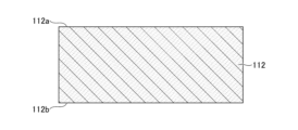
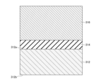
- FIG. 1 is a cross-sectional view (part 1) showing a method for manufacturing a semiconductor device according to a first embodiment.
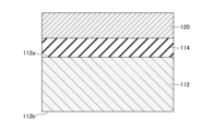
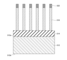
- FIG. 2 is a cross-sectional view (part 2) showing the method for manufacturing the semiconductor device according to the first embodiment.
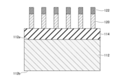
- FIG. 3 is a cross-sectional view (part 3) showing the method for manufacturing the semiconductor device according to the first embodiment.
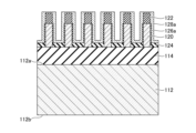
- FIG. 4 is a cross-sectional view (part 4) showing the method for manufacturing the semiconductor device according to the first embodiment.
- FIG. 5 is a cross-sectional view (part 5) showing the method for manufacturing the semiconductor device according to the first embodiment.
- FIG. 6 is a cross-sectional view (part 6) showing the method for manufacturing the semiconductor device according to the first embodiment.
- FIG. 1 is a cross-sectional view (part 1) showing a method for manufacturing a semiconductor device according to a first embodiment.
- FIG. 2 is a cross-sectional view (part 2) showing the method for manufacturing the semiconductor device according to the first embodiment.
- FIG. 3 is
- FIG. 7 is a cross-sectional view (part 7) showing the method for manufacturing the semiconductor device according to the first embodiment.
- FIG. 8 is a cross-sectional view (part 8) showing the method for manufacturing the semiconductor device according to the first embodiment.
- FIG. 9 is a cross-sectional view (part 9) showing the method for manufacturing the semiconductor device according to the first embodiment.
- FIG. 10 is a cross-sectional view (part 10) showing the method for manufacturing the semiconductor device according to the first embodiment.
- FIG. 11 is a cross-sectional view (part 11) showing the method for manufacturing the semiconductor device according to the first embodiment.
- FIG. 12 is a cross-sectional view (part 12) showing the method for manufacturing the semiconductor device according to the first embodiment.
- FIG. 13 is a cross-sectional view (part 1) showing the method for manufacturing the semiconductor device according to the second embodiment.
- FIG. 14 is a cross-sectional view (part 2) showing the method for manufacturing the semiconductor device according to the second embodiment.
- FIG. 15 is a cross-sectional view (part 3) showing the method for manufacturing the semiconductor device according to the second embodiment.
- FIG. 16 is a cross-sectional view (part 4) showing the method for manufacturing the semiconductor device according to the second embodiment.
- FIG. 17 is a cross-sectional view (part 5) showing the method for manufacturing the semiconductor device according to the second embodiment.
- FIG. 18 is a cross-sectional view (part 6) showing the method for manufacturing the semiconductor device according to the second embodiment.
- FIG. 19 is a cross-sectional view (part 7) showing the method for manufacturing the semiconductor device according to the second embodiment.
- FIG. 20 is a cross-sectional view (part 8) showing the method for manufacturing the semiconductor device according to the second embodiment.
- FIG. 21 is a cross-sectional view (part 9) showing the method for manufacturing the semiconductor device according to the second embodiment.
- FIG. 22 is a cross-sectional view (part 10) showing the method for manufacturing the semiconductor device according to the second embodiment.
- FIG. 23 is a cross-sectional view (part 11) showing the method for manufacturing the semiconductor device according to the second embodiment.
- FIG. 24 is a cross-sectional view (part 1) showing the method for manufacturing the semiconductor device according to the third embodiment.
- FIG. 25 is a cross-sectional view (part 2) showing the method for manufacturing the semiconductor device according to the third embodiment.
- FIG. 26 is a cross-sectional view (part 3) showing the method for manufacturing the semiconductor device according to the third embodiment.
- FIG. 27 is a cross-sectional view (part 4) showing the method for manufacturing the semiconductor device according to the third embodiment.
- FIG. 28 is a cross-sectional view (part 5) showing the method for manufacturing the semiconductor device according to the third embodiment.
- FIG. 29 is a cross-sectional view (part 6) showing the method for manufacturing the semiconductor device according to the third embodiment.
- FIG. 30 is a cross-sectional view (part 7) showing the method for manufacturing the semiconductor device according to the third embodiment.
- FIG. 31 is a cross-sectional view (part 8) showing the method for manufacturing the semiconductor device according to the third embodiment.
- FIG. 32 is a cross-sectional view (part 9) showing the method for manufacturing the semiconductor device according to the third embodiment.
- FIG. 33 is a cross-sectional view (part 10) showing the method for manufacturing the semiconductor device according to the third embodiment.
- FIG. 34 is a cross-sectional view (part 11) showing the method for manufacturing the semiconductor device according to the third embodiment.
- FIG. 35 is a cross-sectional view (part 12) showing the method for manufacturing the semiconductor device according to the third embodiment.
- FIG. 36 is a cross-sectional view (part 13) showing the method for manufacturing the semiconductor device according to the third embodiment.
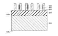
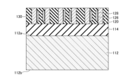
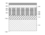
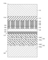
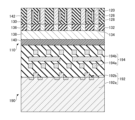
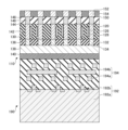
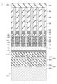
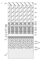
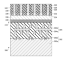
- Figures 1 to 12 are cross-sectional views showing the method for manufacturing a semiconductor device 1 according to the first embodiment.
- a silicon substrate 112 is prepared.
- the silicon substrate 112 has a first main surface 112a and a second main surface 112b.
- the second main surface 112b is the surface opposite to the first main surface 112a.
- the silicon substrate 112 is a silicon single crystal substrate.
- a silicon oxide film 114, an amorphous silicon film 116, and a metal layer 118 are formed in this order on the first main surface 112a of the silicon substrate 112.
- the silicon oxide film 114 is formed on the first main surface 112a of the silicon substrate 112 by chemical vapor deposition (CVD), thermal oxidation, or the like.
- the amorphous silicon film 116 is formed on the silicon oxide film 114 by CVD or the like.
- the metal layer 118 is formed on the amorphous silicon film 116 by CVD, physical vapor deposition (PVD), or the like.
- the metal layer 118 is formed of, for example, nickel (Ni), nickel-aluminum alloy (Ni-Al), cobalt (Co), or palladium (Pd). Next, alloying annealing may be performed. As a result, at least a portion of the metal layer 118 reacts with the silicon (Si) that constitutes the amorphous silicon film 116 and becomes a silicide.
- the silicon substrate 112 on which the metal layer 118 is formed is annealed to change the amorphous silicon film 116 into a crystalline silicon film 120.
- the amorphous silicon film 116 is crystallized to form the crystalline silicon film 120 by metal-induced crystallization (MIC), metal-induced lateral crystallization (MILC), or the like.
- MIC metal-induced crystallization
- MILC metal-induced lateral crystallization
- the silicon substrate 112 on which the metal layer 118 is formed is annealed at a predetermined temperature in an inert gas atmosphere.
- the metal constituting the metal layer 118 diffuses into the amorphous silicon film 116, and the amorphous silicon film 116 is crystallized by metal-induced crystallization or metal-induced lateral crystallization using the metal diffused into the amorphous silicon film 116 as a nucleus to form the crystalline silicon film 120.
- the metal constituting the metal layer 118 may also diffuse into the silicon oxide film 114.
- the metal layer 118 is removed by wet etching or the like.
- the crystalline silicon film 120 is processed into a columnar shape.
- a thin film for the hard mask 122 is formed on the crystalline silicon film 120 by CVD or the like.
- the thin film for the hard mask 122 is, for example, a SiN film or a SiO 2 film.
- a resist mask having an opening other than the region where the crystalline silicon film 120 is to be left is formed by lithography.
- the crystalline silicon film 120 is etched and removed using the resist mask.
- the resist mask is removed.
- the crystalline silicon film 120 is processed into a columnar shape extending in a direction perpendicular to the first main surface 112a.
- a gate stack structure is formed.
- an insulating film 124 is formed on the silicon oxide film 114.
- the insulating film 124 is, for example, a SiN film, a SiOCN film, or a SiOC film.
- an insulating film 126a for the gate insulating film 126 is formed on the side surface of the crystalline silicon film 120 by thermal oxidation, ALD, or the like.
- the insulating film 126a is, for example, a SiO 2 film or a high-k film.
- a metal film 128a for the gate electrode 128 is formed so as to cover the crystalline silicon film 120, the hard mask 122, the insulating film 124, and the insulating film 126a.
- the metal film 128a is, for example, formed of tungsten (W), cobalt, or molybdenum (Mo).
- the gate insulating film 126 and the gate electrode 128 are formed.
- the insulating film 126a and the metal film 128a are etched by etch-back or the like, and the insulating film 126a and the metal film 128a are left on a part of the side of the crystalline silicon film 120.
- the hard mask 122 is etched and removed by wet etching, dry etching, or the like.
- the insulating film 124 is etched and removed by wet etching, dry etching, or the like.
- the gate insulating film 126 is formed from the insulating film 126a
- the gate electrode 128 is formed from the metal film 128a.
- the gate insulating film 126 and the gate electrode 128 are formed, for example, in the central part of the crystalline silicon film 120 in a direction perpendicular to the first main surface 112a.
- the gate electrode 128 is electrically connected to a word line (not shown).
- the interlayer insulating film 130 is formed.
- an insulating film for the interlayer insulating film 130 is formed so as to cover the silicon oxide film 114, the crystalline silicon film 120, the gate insulating film 126, and the gate electrode 128.
- the insulating film for the interlayer insulating film 130 is, for example, a SiO 2 film, a SiOCN film, or a SiOC film.
- CMP chemical mechanical polishing
- ion implantation is performed on the bit line 138 side of the crystalline silicon film 120.
- a source region (not shown) is formed by ion implantation.
- n-type impurities such as arsenic (As) and phosphorus (P) are ion-implanted.
- the source region is electrically connected to the bit line 138.
- activation annealing is performed by RTA (Rapid Thermal Anneal), a heating furnace, or the like.
- a bit line 138 is formed.
- an insulating film for the interlayer insulating film 132 is formed on the crystalline silicon film 120 and the interlayer insulating film 130.
- the insulating film for the interlayer insulating film 132 is, for example, a SiO 2 film, a SiOCN film, or a SiOC film.
- a resist mask having an opening is formed on the crystalline silicon film 120 by lithography.
- the insulating film for the interlayer insulating film 132 is etched and removed by dry etching or the like using the resist mask. As a result, a via 134 is formed in which the crystalline silicon film 120 is exposed.
- a metal film is formed so that the via 134 is filled, and the surface is flattened by CMP or the like.
- a metal film 136 is formed inside the via 134.
- the metal film 136 is formed of, for example, titanium nitride (TiN), tungsten, cobalt, molybdenum, or ruthenium (Ru).
- an insulating film for an interlayer insulating film (not shown) that insulates between the bit lines 138 is formed on the interlayer insulating film 132 and the metal film 136.
- the insulating film for the interlayer insulating film is, for example, a SiO 2 film, a SiOCN film, or a SiOC film.
- a resist mask having an opening in the region where the bit line 138 is to be formed is formed by lithography.
- the insulating film for the interlayer insulating film is etched by dry etching or the like using the resist mask.
- a trench is formed in which the interlayer insulating film 132 and the metal film 136 are exposed.
- a metal film for the bit line 138 is formed so that the trench is filled, and the surface is flattened by CMP or the like.
- the bit line 138 is formed inside the trench.
- the bit line 138 is formed of titanium nitride, tungsten, cobalt, molybdenum, or ruthenium.
- an interlayer insulating film 140 is formed on the bit line 138 and the interlayer insulating film that insulates between the bit lines 138.
- the interlayer insulating film 140 is, for example, a SiO 2 film, a SiOCN film, or a SiOC film.
- the first main surface 112a of the first substrate 110 on which the interlayer insulating film 140 has been formed is bonded to a second substrate 190 prepared in advance.
- the second substrate 190 is a CMOS (Complementary Metal Oxide Semiconductor) substrate.
- the second substrate 190 has a CMOS section 192 and a wiring section 194.
- the CMOS section 192 includes a silicon substrate 192a and a plurality of transistors 192b.
- the plurality of transistors 192b include a P-type transistor and an N-type transistor.
- the wiring section 194 includes a wiring 194a and an interlayer insulating film 194b.
- the wiring 194a is formed in multiple layers.
- the interlayer insulating film 194b provides insulation between the wirings 194a.
- the first substrate 110 and the second substrate 190 are bonded so that the interlayer insulating film 140 and the wiring section 194 are in contact with each other.
- the silicon substrate 112 and the silicon oxide film 114 are removed from the second main surface 112b side of the silicon substrate 112 to thin the first substrate 110.
- first, grinding and CMP are performed in this order to polish the silicon substrate 112 from the second main surface 112b side.
- the silicon substrate 112 is selectively etched and removed with respect to the silicon oxide film 114 by wet etching, dry etching, or the like. Instead of grinding, the silicon substrate 112 may be removed by laser lift-off or a peeling technique using a laser.
- a peeling layer is provided between the silicon substrate 112 and the silicon oxide film 114, and the peeling layer is peeled off by laser irradiation, thereby removing the silicon substrate 112 together with the peeling layer.
- a peeling technique using a laser for example, a modified layer is formed inside the silicon substrate 112 by laser irradiation, and the silicon substrate 112 can be removed starting from the modified layer.
- the silicon oxide film 114 is selectively etched with respect to the crystalline silicon film 120 and the interlayer insulating film 130 to remove it. In this case, metal that may diffuse into the silicon oxide film 114 is removed together with the silicon oxide film 114, so that it does not remain in the final semiconductor device 1.
- ion implantation is performed on the capacitor 160 side of the crystalline silicon film 120.
- a drain region (not shown) is formed by ion implantation.
- a transistor 142 is formed with a channel (not shown) between the source region and the drain region of the crystalline silicon film 120.
- n-type impurities such as arsenic and phosphorus are ion implanted.
- the drain region is electrically connected to the capacitor 160.
- activation annealing is performed using RTA, a heating furnace, etc.
- a pad 154 for the capacitor 160 is formed.
- an insulating film for the interlayer insulating film 144 is formed on the crystalline silicon film 120 and the interlayer insulating film 130.
- the insulating film for the interlayer insulating film 144 is, for example, a SiO 2 film, a SiOCN film, or a SiOC film.
- a resist mask having an opening is formed on the crystalline silicon film 120 by lithography.
- the insulating film for the interlayer insulating film 144 is etched and removed by dry etching or the like using the resist mask. As a result, a via 146 is formed in which the crystalline silicon film 120 is exposed.
- a metal film is formed so that the via 146 is filled, and the surface is flattened by CMP or the like.
- a metal film 148 is formed inside the via 146.
- the metal film 148 is formed of, for example, titanium nitride, tungsten, cobalt, molybdenum, or ruthenium.
- an insulating film for the interlayer insulating film 150 is formed on the interlayer insulating film 144 and the metal film 148.
- the insulating film for the interlayer insulating film 150 is, for example, a SiO2 film, a SiOCN film, or a SiOC film.
- a resist mask having an opening is formed on the metal film 148 by lithography.
- the insulating film for the interlayer insulating film 150 is etched and removed by dry etching or the like using the resist mask. As a result, an opening 152 is formed in which the metal film 148 is exposed. Next, a metal film is formed so as to fill the opening 152, and the surface is flattened by CMP or the like. As a result, a pad 154 is formed inside the opening 152.
- the pad 154 is formed of, for example, titanium nitride, tungsten, cobalt, molybdenum, or ruthenium.
- a capacitor 160 is formed adjacent to the transistor 142 in a direction perpendicular to the first main surface 112a and electrically connected to the transistor 142.
- an insulating film for the interlayer insulating film 156 is formed on the interlayer insulating film 150 and the pad 154.
- the insulating film for the interlayer insulating film 156 is, for example, a SiO 2 film, a SiOCN film, or a SiOC film.
- a resist mask having an opening on the pad 154 is formed by lithography.
- the insulating film for the interlayer insulating film 156 is etched and removed by dry etching or the like using the resist mask.
- the capacitor 160 has a structure in which an insulating film is sandwiched between, for example, metal films.
- an insulating film 162 is formed to cover the upper surface of the interlayer insulating film 156 and the upper surface of the capacitor 160.
- the semiconductor device 1 is configured as a DRAM (Dynamic Random Access Memory) having a plurality of memory cells 164.
- Each memory cell 164 includes a transistor 142 and a capacitor 160 connected in series.
- a silicon substrate 112 having a first main surface 112a is prepared.
- a silicon oxide film 114, an amorphous silicon film 116, and a metal layer 118 are formed in this order on the first main surface 112a of the silicon substrate 112.
- the silicon substrate 112 on which the metal layer 118 is formed is annealed to change the amorphous silicon film 116 into a crystalline silicon film 120.
- a transistor 142 is formed in which a part of the crystalline silicon film 120 serves as a channel.
- a capacitor 160 is formed adjacent to the transistor 142 in a direction perpendicular to the first main surface 112a and electrically connected to the transistor 142.
- a semiconductor device 1 including a transistor 142 in which a part of the crystalline silicon film 120 serves as a channel can be formed without using an SOI substrate.
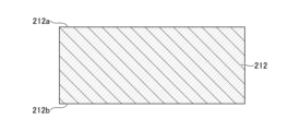
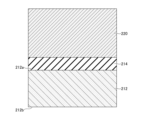
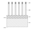
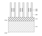
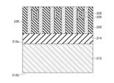
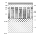
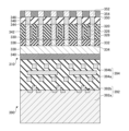
- Figures 13 to 23 are cross-sectional views showing the method for manufacturing the semiconductor device 2 according to the second embodiment.
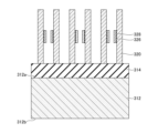
- a silicon substrate 212 is prepared.
- the silicon substrate 212 has a first main surface 212a and a second main surface 212b.
- the second main surface 212b is the surface opposite to the first main surface 212a.
- the silicon substrate 212 is a silicon single crystal substrate.
- a silicon oxide film 214, an amorphous silicon film 216, and a metal layer 218 are formed in this order on the first main surface 212a of the silicon substrate 212.
- the silicon oxide film 214 is formed on the first main surface 212a of the silicon substrate 212 by CVD, thermal oxidation, or the like.
- the amorphous silicon film 216 is formed on the silicon oxide film 214 by CVD or the like. The amorphous silicon film 216 is deposited so as to be thicker than the film thickness of the crystalline silicon film 220 remaining in the final semiconductor device 2.
- the film thickness of the amorphous silicon film 216 may be twice or more the film thickness of the crystalline silicon film 220 remaining in the final semiconductor device 2.
- a metal layer 218 is formed on the amorphous silicon film 216 by CVD, PVD, or the like.
- the metal layer 218 can be formed in the same manner as the metal layer 118.
- the silicon substrate 212 on which the metal layer 218 is formed is annealed to change the amorphous silicon film 216 into a crystalline silicon film 220.
- the crystalline silicon film 220 can be formed in the same manner as the crystalline silicon film 120.
- the crystalline silicon film 220 is processed into a columnar shape.
- a thin film for the hard mask 222 is formed on the crystalline silicon film 220 by CVD or the like.
- the thin film for the hard mask 222 is, for example, a SiN film or a SiO 2 film.
- a resist mask having an opening other than the region where the crystalline silicon film 220 is to be left is formed by lithography.
- the crystalline silicon film 220 is etched and removed using the resist mask.
- the resist mask is removed.
- the crystalline silicon film 220 is processed into a columnar shape extending in a direction perpendicular to the first main surface 212a.
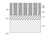
- a gate insulating film 226 and a gate electrode 228 are formed.
- the gate insulating film 226 and the gate electrode 228 can be formed in the same manner as the gate insulating film 126 and the gate electrode 128.
- the gate insulating film 226 and the gate electrode 228 are formed in the central portion of the crystalline silicon film 220 in a direction perpendicular to the first main surface 212a, for example.
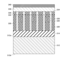
- an interlayer insulating film 230 is formed.
- an insulating film for the interlayer insulating film 230 is formed so as to cover the silicon oxide film 214, the crystalline silicon film 220, the gate insulating film 226, and the gate electrode 228.
- the insulating film for the interlayer insulating film 230 is, for example, a SiO 2 film, a SiOCN film, or a SiOC film.
- the upper surface of the crystalline silicon film 220 is exposed by CMP or the like. This forms the interlayer insulating film 230.
- the crystalline silicon film 220 is polished to the vicinity of the gate electrode 228 to reduce the film thickness.
- the vicinity of the starting point region of the metal-induced crystallization or metal-induced lateral crystallization of the crystalline silicon film 220 is removed.
- the vicinity of the starting point region of the metal-induced crystallization or metal-induced lateral crystallization is prone to poor crystallinity or uneven crystallinity. Therefore, by removing the vicinity of the starting point region of metal-induced crystallization or metal-induced lateral crystallization, the crystalline silicon film 220 with good crystallinity can be used as a channel.
- ion implantation is performed on the bit line 238 side of the crystalline silicon film 220. For example, a source region (not shown) is formed by ion implantation.
- n-type impurities such as arsenic and phosphorus are ion-implanted.
- the source region is electrically connected to the bit line 238.
- activation annealing is performed by RTA, a heating furnace, or the like.
- a bit line 238 is formed.
- an insulating film for the interlayer insulating film 232 is formed on the crystalline silicon film 220 and the interlayer insulating film 230.
- the insulating film for the interlayer insulating film 232 is, for example, a SiO 2 film, a SiOCN film, or a SiOC film.
- a resist mask having an opening is formed on the crystalline silicon film 220 by lithography.
- the insulating film for the interlayer insulating film 232 is etched and removed by dry etching or the like using the resist mask. As a result, a via 234 is formed in which the crystalline silicon film 220 is exposed.
- a metal film is formed so that the via 234 is filled, and the surface is flattened by CMP or the like.
- a metal film 236 is formed inside the via 234.
- the metal film 236 is formed of, for example, titanium nitride, tungsten, cobalt, molybdenum, or ruthenium.
- an insulating film for an interlayer insulating film (not shown) that insulates between the bit lines 238 is formed on the interlayer insulating film 232 and the metal film 236.
- the insulating film for the interlayer insulating film is, for example, a SiO 2 film, a SiOCN film, or a SiOC film.
- a resist mask having an opening in the region where the bit line 238 is to be formed is formed by lithography.
- the insulating film for the interlayer insulating film is etched by dry etching or the like using the resist mask.
- a trench is formed in which the interlayer insulating film 232 and the metal film 236 are exposed.
- a metal film for the bit line 238 is formed so that the trench is filled, and the surface is flattened by CMP or the like.
- the bit line 238 is formed inside the trench.
- the bit line 238 is formed of titanium nitride, tungsten, cobalt, molybdenum, or ruthenium.
- an interlayer insulating film 240 is formed on the bit line 238 and the interlayer insulating film that insulates between the bit lines 238.
- the interlayer insulating film 240 is, for example, a SiO 2 film, a SiOCN film, or a SiOC film.
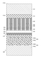
- the first main surface 212a of the first substrate 210 on which the interlayer insulating film 240 has been formed is bonded to a second substrate 290 prepared in advance.
- the second substrate 290 is a CMOS substrate.
- the second substrate 290 has a CMOS section 292 and a wiring section 294.
- the CMOS section 292 includes a silicon substrate 292a and a plurality of transistors 292b.
- the plurality of transistors 292b include a P-type transistor and an N-type transistor.
- the wiring section 294 includes a wiring 294a and an interlayer insulating film 294b.
- the wiring 294a is formed in multiple layers.
- the interlayer insulating film 294b insulates between the wirings 294a.
- the first substrate 210 and the second substrate 290 are bonded so that the interlayer insulating film 240 and the wiring section 294 are in contact with each other.
- the first substrate 210 is thinned by removing the silicon substrate 212, the silicon oxide film 214, a portion of the crystalline silicon film 220, and a portion of the interlayer insulating film 230 from the second main surface 212b side of the silicon substrate 212.
- grinding and CMP are first performed in this order to polish and remove the silicon substrate 212, the silicon oxide film 214, a portion of the crystalline silicon film 220, and a portion of the interlayer insulating film 230 from the second main surface 212b side.
- metal that may diffuse into the silicon oxide film 214 is removed together with the silicon oxide film 214, so that it does not remain in the final semiconductor device 2.
- the crystalline silicon film 220 When polishing a portion of the crystalline silicon film 220, the crystalline silicon film 220 is polished to the vicinity of the gate electrode 228 to reduce the film thickness. In this case, the crystalline silicon film 220 is removed near the end point region of the metal-induced crystallization or metal-induced lateral crystallization of the crystalline silicon film 220.
- the vicinity of the end point region of the metal-induced crystallization or metal-induced lateral crystallization is prone to poor crystallinity or non-uniform crystallinity. Therefore, by removing the vicinity of the end point region of the metal-induced crystallization or metal-induced lateral crystallization, the crystalline silicon film 220 with good crystallinity can be used as a channel.
- ion implantation is performed on the capacitor 260 side of the crystalline silicon film 220.
- a drain region (not shown) is formed by ion implantation.
- a transistor 242 is formed in which a channel (not shown) is formed between the source region and the drain region of the crystalline silicon film 220.
- n-type impurities such as arsenic and phosphorus are ion-implanted.
- the drain region is electrically connected to the capacitor 260.
- activation annealing is performed by RTA, a heating furnace, or the like.
- a pad 254 for the capacitor 260 is formed.
- an insulating film for the interlayer insulating film 244 is formed on the crystalline silicon film 220 and the interlayer insulating film 230.
- the insulating film for the interlayer insulating film 244 is, for example, a SiO 2 film, a SiOCN film, or a SiOC film.
- a resist mask having an opening is formed on the crystalline silicon film 220 by lithography.
- the insulating film for the interlayer insulating film 244 is etched and removed by dry etching or the like using the resist mask. As a result, a via 246 is formed in which the crystalline silicon film 220 is exposed.
- a metal film is formed so that the via 246 is filled, and the surface is flattened by CMP or the like.
- a metal film 248 is formed inside the via 246.
- the metal film 248 is formed of, for example, titanium nitride, tungsten, cobalt, molybdenum, or ruthenium.
- an insulating film for the interlayer insulating film 250 is formed on the interlayer insulating film 244 and the metal film 248.
- the insulating film for the interlayer insulating film 250 is, for example, a SiO2 film, a SiOCN film, or a SiOC film.
- a resist mask having an opening is formed on the metal film 248 by lithography.
- the insulating film for the interlayer insulating film 250 is etched and removed by dry etching or the like using the resist mask. As a result, an opening 252 is formed in which the metal film 248 is exposed. Next, a metal film is formed so as to fill the opening 252, and the surface is flattened by CMP or the like. As a result, a pad 254 is formed inside the opening 252.
- the pad 254 is formed of, for example, titanium nitride, tungsten, cobalt, molybdenum, or ruthenium.
- a capacitor 260 is formed adjacent to the transistor 242 in a direction perpendicular to the first main surface 212a and electrically connected to the transistor 242.
- an insulating film for the interlayer insulating film 256 is formed on the interlayer insulating film 250 and the pad 254.
- the insulating film for the interlayer insulating film 256 is, for example, a SiO 2 film, a SiOCN film, or a SiOC film.
- a resist mask having an opening on the pad 254 is formed by lithography.
- the insulating film for the interlayer insulating film 256 is etched and removed by dry etching or the like using the resist mask.
- the capacitor 260 has a structure in which an insulating film is sandwiched between, for example, metal films.
- an insulating film 262 is formed to cover the upper surface of the interlayer insulating film 256 and the upper surface of the capacitor 260.
- the semiconductor device 2 is configured as a DRAM having a plurality of memory cells 264.
- Each memory cell 264 includes a transistor 242 and a capacitor 260 connected in series.
- a silicon substrate 212 having a first main surface 212a is prepared.
- a silicon oxide film 214, an amorphous silicon film 216, and a metal layer 218 are formed in this order on the first main surface 212a of the silicon substrate 212.
- the silicon substrate 212 on which the metal layer 218 is formed is annealed to change the amorphous silicon film 216 into a crystalline silicon film 220.
- a transistor 242 is formed in which a part of the crystalline silicon film 220 serves as a channel.
- a capacitor 260 is formed adjacent to the transistor 242 in a direction perpendicular to the first main surface 212a and electrically connected to the transistor 242.
- a semiconductor device 2 including a transistor 242 in which a part of the crystalline silicon film 220 serves as a channel can be formed without using an SOI substrate.
- the vicinity of the start point region and the vicinity of the end point region of the metal-induced crystallization or metal-induced lateral crystallization in the crystalline silicon film 220 are removed.
- the crystalline silicon film 220 with good crystallinity can be used as a channel.
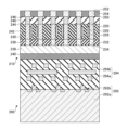
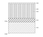
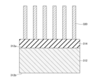
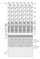
- Figures 24 to 36 are cross-sectional views showing the method for manufacturing the semiconductor device 3 according to the third embodiment.
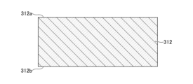
- a silicon substrate 312 is prepared.
- the silicon substrate 312 has a first main surface 312a and a second main surface 312b.
- the second main surface 312b is the surface opposite to the first main surface 312a.
- the silicon substrate 312 is a silicon single crystal substrate.
- a silicon oxide film 314 and an amorphous silicon film 316 are formed in this order on the first main surface 312a of the silicon substrate 312.
- the silicon oxide film 314 is formed on the first main surface 312a of the silicon substrate 312 by CVD, thermal oxidation, or the like.
- the amorphous silicon film 316 is formed on the silicon oxide film 314 by CVD or the like.
- the amorphous silicon film 316 is deposited to the same thickness as the amorphous silicon film 216, for example.
- the amorphous silicon film 316 is processed into a columnar shape.
- a thin film for a hard mask 322 is formed on the amorphous silicon film 316 by CVD or the like.
- the thin film for the hard mask 322 is, for example, a SiN film or a SiO 2 film.
- a resist mask having an opening in an area other than the area where the amorphous silicon film 316 is to be left is formed by lithography.
- the amorphous silicon film 316 is etched and removed using the resist mask.
- the resist mask is removed.
- the amorphous silicon film 316 is processed into a columnar shape extending in a direction perpendicular to the first main surface 312a.
- a gettering film 372 and a metal layer 318 are formed.
- the hard mask 322 is etched and removed by wet etching, dry etching, or the like.
- a thin film for the gettering film 372 is formed so as to cover the side and upper surface of the amorphous silicon film 316.
- the thin film for the gettering film 372 is, for example, a SiO 2 film, a SiN film, or a polysilicon film to which impurities are added.
- the upper surface of the amorphous silicon film 316 is exposed by CMP or the like. This forms the gettering film 372.
- a metal layer 318 is formed on the amorphous silicon film 316 and the gettering film 372 by CVD, PVD, or the like.
- the metal layer 318 can be formed in the same manner as the metal layer 118.
- the silicon substrate 312 on which the metal layer 318 is formed is annealed to change the amorphous silicon film 316 into a crystalline silicon film 320.
- the amorphous silicon film 316 is crystallized by metal-induced crystallization, metal-induced lateral crystallization, or the like to form the crystalline silicon film 320.
- the silicon substrate 312 on which the metal layer 318 is formed is annealed at a predetermined temperature.
- the metal constituting the metal layer 318 diffuses into the amorphous silicon film 316, and the amorphous silicon film 316 is crystallized by metal-induced crystallization or metal-induced lateral crystallization using the metal diffused into the amorphous silicon film 316 as a nucleus to form the crystalline silicon film 320.
- the metal constituting the metal layer 318 may remain in the crystalline silicon film 320.
- the concentration of the metal remaining in the crystalline silicon film 320 can be reduced by diffusing the remaining metal from the crystalline silicon film 320 to the silicon oxide film 114 and the gettering film 372.
- the reliability of the transistor 342, which uses the crystalline silicon film 320 as a channel can be improved.
- the metal layer 318 is removed by wet etching or the like.
- the gettering film 372 is etched and removed by dry etching, wet etching, or the like. This makes it possible to prevent the metal in the gettering film 372 from being re-incorporated into the crystalline silicon film 320.
- a gate insulating film 326 and a gate electrode 328 are formed.
- the gate insulating film 326 and the gate electrode 328 can be formed in the same manner as the gate insulating film 126 and the gate electrode 128.
- the gate insulating film 326 and the gate electrode 328 are formed, for example, in the central portion of the crystalline silicon film 320 in a direction perpendicular to the first main surface 312a.
- an interlayer insulating film 330 is formed.
- an insulating film for the interlayer insulating film 330 is formed so as to cover the silicon oxide film 314, the crystalline silicon film 320, the gate insulating film 326, and the gate electrode 328.
- the insulating film for the interlayer insulating film 330 is, for example, a SiO 2 film, a SiOCN film, or a SiOC film.
- the upper surface of the crystalline silicon film 320 is exposed by CMP or the like. This forms the interlayer insulating film 330.
- the crystalline silicon film 320 is polished to the vicinity of the gate electrode 328 to reduce the film thickness.
- the vicinity of the starting point region of the metal-induced crystallization or the metal-induced lateral crystallization of the crystalline silicon film 320 is removed.
- the vicinity of the starting point region of the metal-induced crystallization or the metal-induced lateral crystallization is likely to have poor crystallinity or uneven crystallinity. Therefore, by removing the vicinity of the starting point region of metal-induced crystallization or metal-induced lateral crystallization, the crystalline silicon film 320 with good crystallinity can be used as a channel.
- ion implantation is performed on the bit line 338 side of the crystalline silicon film 320. For example, a source region (not shown) is formed by ion implantation.
- n-type impurities such as arsenic and phosphorus are ion-implanted.
- the source region is electrically connected to the bit line 338.
- activation annealing is performed by RTA, a heating furnace, or the like.
- a bit line 338 is formed.
- an insulating film for the interlayer insulating film 332 is formed on the crystalline silicon film 320 and the interlayer insulating film 330.
- the insulating film for the interlayer insulating film 332 is, for example, a SiO 2 film, a SiOCN film, or a SiOC film.
- a resist mask having an opening is formed on the crystalline silicon film 320 by lithography.
- the insulating film for the interlayer insulating film 332 is etched and removed by dry etching or the like using the resist mask. As a result, a via 334 is formed in which the crystalline silicon film 320 is exposed.
- a metal film is formed so that the via 334 is filled, and the surface is planarized by CMP or the like.
- a metal film 336 is formed inside the via 334.
- the metal film 336 is formed of, for example, titanium nitride, tungsten, cobalt, molybdenum, or ruthenium.
- an insulating film for an interlayer insulating film (not shown) that insulates between the bit lines 338 is formed on the interlayer insulating film 332 and the metal film 336.
- the insulating film for the interlayer insulating film is, for example, a SiO 2 film, a SiOCN film, or a SiOC film.
- a resist mask having an opening in a region where the bit line 338 is to be formed is formed by lithography.
- the insulating film for the interlayer insulating film is etched by dry etching or the like using the resist mask.
- a trench is formed in which the interlayer insulating film 332 and the metal film 336 are exposed.
- a metal film for the bit line 338 is formed so that the trench is filled, and the surface is flattened by CMP or the like.
- the bit line 338 is formed inside the trench.
- the bit line 338 is formed of titanium nitride, tungsten, cobalt, molybdenum, or ruthenium.
- an interlayer insulating film 340 is formed on the bit line 338 and the interlayer insulating film that insulates between the bit lines 338.
- the interlayer insulating film 340 is, for example, a SiO 2 film, a SiOCN film, or a SiOC film.
- the first main surface 312a of the first substrate 310 on which the interlayer insulating film 340 has been formed is bonded to a second substrate 390 prepared in advance.
- the second substrate 390 is a CMOS substrate.
- the second substrate 390 has a CMOS section 392 and a wiring section 394.
- the CMOS section 392 includes a silicon substrate 392a and a plurality of transistors 392b.
- the plurality of transistors 392b include a P-type transistor and an N-type transistor.
- the wiring section 394 includes a wiring 394a and an interlayer insulating film 394b.
- the wiring 394a is formed in multiple layers.
- the interlayer insulating film 394b insulates between the wirings 394a.
- the first substrate 310 and the second substrate 390 are bonded so that the interlayer insulating film 340 and the wiring section 394 are in contact with each other.
- the first substrate 310 is thinned by removing the silicon substrate 312, the silicon oxide film 314, a portion of the crystalline silicon film 320, and a portion of the interlayer insulating film 330 from the second main surface 312b side of the silicon substrate 312.
- grinding and CMP are first performed in this order to polish and remove the silicon substrate 312, the silicon oxide film 314, a portion of the crystalline silicon film 320, and a portion of the interlayer insulating film 330 from the second main surface 312b side.
- metal that may diffuse into the silicon oxide film 314 is removed together with the silicon oxide film 314, so that it does not remain in the final semiconductor device 3.
- the crystalline silicon film 320 When polishing a portion of the crystalline silicon film 320, the crystalline silicon film 320 is polished to the vicinity of the gate electrode 328 to reduce the film thickness. In this case, the crystalline silicon film 320 is removed near the end point region of the metal-induced crystallization or metal-induced lateral crystallization of the crystalline silicon film 320.
- the vicinity of the end point region of metal-induced crystallization or metal-induced lateral crystallization is prone to poor crystallinity or non-uniform crystallinity. Therefore, by removing the vicinity of the end point region of metal-induced crystallization or metal-induced lateral crystallization, the crystalline silicon film 320 with good crystallinity can be used as a channel.
- ion implantation is performed on the capacitor 360 side of the crystalline silicon film 320.
- a drain region (not shown) is formed by ion implantation.
- a transistor 342 is formed in which a channel (not shown) is formed between the source region and the drain region of the crystalline silicon film 320.
- n-type impurities such as arsenic and phosphorus are ion-implanted.
- the drain region is electrically connected to the capacitor 360.
- activation annealing is performed by RTA, a heating furnace, or the like.
- a pad 354 for the capacitor 360 is formed.
- an insulating film for the interlayer insulating film 344 is formed on the crystalline silicon film 320 and the interlayer insulating film 330.
- the insulating film for the interlayer insulating film 344 is, for example, a SiO 2 film, a SiOCN film, or a SiOC film.
- a resist mask having an opening is formed on the crystalline silicon film 320 by lithography.
- the insulating film for the interlayer insulating film 344 is etched and removed by dry etching or the like using the resist mask. As a result, a via 346 is formed in which the crystalline silicon film 320 is exposed.
- a metal film is formed so that the via 346 is filled, and the surface is flattened by CMP or the like.
- a metal film 348 is formed inside the via 346.
- the metal film 348 is formed of, for example, titanium nitride, tungsten, cobalt, molybdenum, or ruthenium.
- an insulating film for the interlayer insulating film 350 is formed on the interlayer insulating film 344 and the metal film 348.
- the insulating film for the interlayer insulating film 350 is, for example, a SiO2 film, a SiOCN film, or a SiOC film.
- a resist mask having an opening is formed on the metal film 348 by lithography.
- the insulating film for the interlayer insulating film 350 is etched and removed by dry etching or the like using the resist mask. As a result, an opening 352 is formed in which the metal film 348 is exposed. Next, a metal film is formed so as to fill the opening 352, and the surface is planarized by CMP or the like. As a result, a pad 354 is formed inside the opening 352.
- the pad 354 is formed of, for example, titanium nitride, tungsten, cobalt, molybdenum, or ruthenium.
- a capacitor 360 is formed adjacent to the transistor 342 in a direction perpendicular to the first main surface 312a and electrically connected to the transistor 342.
- an insulating film for the interlayer insulating film 356 is formed on the interlayer insulating film 350 and the pad 354.
- the insulating film for the interlayer insulating film 356 is, for example, a SiO 2 film, a SiOCN film, or a SiOC film.
- a resist mask having an opening on the pad 354 is formed by lithography.
- the insulating film for the interlayer insulating film 356 is etched and removed by dry etching or the like using the resist mask.
- capacitor hole 358 This forms a capacitor hole 358 in which the pad 354 is exposed.
- a capacitor 360 is formed inside the capacitor hole 358.
- the capacitor 360 has a structure in which an insulating film is sandwiched between, for example, metal films.
- an insulating film 362 is formed to cover the upper surface of the interlayer insulating film 356 and the upper surface of the capacitor 360.
- the semiconductor device 3 is configured as a DRAM having a plurality of memory cells 364.
- Each memory cell 364 includes a transistor 342 and a capacitor 360 connected in series.
- a silicon substrate 312 having a first main surface 312a is prepared.
- a silicon oxide film 314, an amorphous silicon film 316, and a metal layer 318 are formed in this order on the first main surface 312a of the silicon substrate 312.
- the silicon substrate 312 on which the metal layer 318 is formed is annealed to change the amorphous silicon film 316 into a crystalline silicon film 320.
- a transistor 342 is formed in which a part of the crystalline silicon film 320 serves as a channel.
- a capacitor 360 is formed adjacent to the transistor 342 in a direction perpendicular to the first main surface 312a and electrically connected to the transistor 342.
- a semiconductor device 3 including a transistor 342 in which a part of the crystalline silicon film 320 serves as a channel can be formed without using an SOI substrate.
- the vicinity of the start point region and the vicinity of the end point region of the metal-induced crystallization or metal-induced lateral crystallization in the crystalline silicon film 320 are removed.
- the crystalline silicon film 320 with good crystallinity can be used as a channel.
Landscapes
- Semiconductor Memories (AREA)
- Engineering & Computer Science (AREA)
- Manufacturing & Machinery (AREA)
- Semiconductor Integrated Circuits (AREA)
Abstract
Description
図1から図12を参照し、第1実施形態に係る半導体装置1の製造方法について説明する。図1から図12は、第1実施形態に係る半導体装置1の製造方法を示す断面図である。
図13から図23を参照し、第2実施形態に係る半導体装置2の製造方法について説明する。図13から図23は、第2実施形態に係る半導体装置2の製造方法を示す断面図である。
図24から図36を参照し、第3実施形態に係る半導体装置3の製造方法について説明する。図24から図36は、第3実施形態に係る半導体装置3の製造方法を示す断面図である。
112、212、312 シリコン基板
112a、212a、312a 第1主面
114、214、314 シリコン酸化膜
116、216、316 非晶質シリコン膜
118、218、318 金属層
120、220、320 結晶シリコン膜
142、242、342 トランジスタ
160、260、360 キャパシタ
Claims (10)
- 第1主面を有するシリコン基板を準備する工程と、
前記シリコン基板の前記第1主面の上にシリコン酸化膜を形成する工程と、
前記シリコン酸化膜の上に非晶質シリコン膜を形成する工程と、
前記非晶質シリコン膜の上に金属層を形成する工程と、
前記金属層が形成された前記シリコン基板をアニールすることにより、前記非晶質シリコン膜を結晶シリコン膜に変化させる工程と、
前記結晶シリコン膜の一部をチャネルとするトランジスタを形成する工程と、
前記第1主面と垂直な方向において前記トランジスタと隣り合い、前記トランジスタと電気的に接続されるキャパシタを形成する工程と、
を有する、半導体装置の製造方法。 - 前記トランジスタを形成する工程は、
前記シリコン基板の前記第1主面の側を第2シリコン基板に接合する工程と、
前記第2シリコン基板に接合された前記シリコン基板の前記第1主面と反対の第2主面の側から前記シリコン基板及び前記シリコン酸化膜を除去する工程と、
を含む、
請求項1に記載の半導体装置の製造方法。 - 前記第2シリコン基板は、CMOS基板である、
請求項2に記載の半導体装置の製造方法。 - 前記結晶シリコン膜は、前記シリコン酸化膜と接する第1面と、前記第1面と反対の第2面とを有し、
前記トランジスタを形成する工程は、前記結晶シリコン膜の前記第2面を研磨して膜厚を減ずる工程を含む、
請求項3に記載の半導体装置の製造方法。 - 前記トランジスタを形成する工程は、前記シリコン基板及び前記シリコン酸化膜を除去する工程の後に、前記結晶シリコン膜の前記第1面を研磨して膜厚を減ずる工程を含む、
請求項4に記載の半導体装置の製造方法。 - 前記シリコン基板及び前記シリコン酸化膜を除去する工程は、レーザリフトオフ又はレーザを用いた剥離技術により前記シリコン基板を除去することを含む、
請求項2に記載の半導体装置の製造方法。 - 前記結晶シリコン膜に変化させる工程と前記トランジスタを形成する工程との間に、前記結晶シリコン膜を前記第1主面と垂直な方向に延在する柱状に加工する工程を有する、
請求項1乃至6のいずれか一項に記載の半導体装置の製造方法。 - 前記非晶質シリコン膜を形成する工程と前記金属層を形成する工程との間に、前記非晶質シリコン膜を前記第1主面と垂直な方向に延在する柱状に加工する工程を有する、
請求項1乃至6のいずれか一項に記載の半導体装置の製造方法。 - 前記柱状に加工する工程と前記金属層を形成する工程との間に、前記非晶質シリコン膜の側面を覆うゲッタリング膜を形成する工程を有する、
請求項8に記載の半導体装置の製造方法。 - 前記金属層を形成する工程の後に、前記ゲッタリング膜を除去する工程を有する、
請求項9に記載の半導体装置の製造方法。
Priority Applications (3)
| Application Number | Priority Date | Filing Date | Title |
|---|---|---|---|
| JP2025557792A JPWO2025105252A1 (ja) | 2023-11-16 | 2024-11-06 | |
| KR1020267017932A KR20260112747A (ko) | 2023-11-16 | 2024-11-06 | 반도체 장치의 제조 방법 |
| CN202480070762.0A CN122162511A (zh) | 2023-11-16 | 2024-11-06 | 半导体装置的制造方法 |
Applications Claiming Priority (2)
| Application Number | Priority Date | Filing Date | Title |
|---|---|---|---|
| JP2023-194952 | 2023-11-16 | ||
| JP2023194952 | 2023-11-16 |
Publications (1)
| Publication Number | Publication Date |
|---|---|
| WO2025105252A1 true WO2025105252A1 (ja) | 2025-05-22 |
Family
ID=95742234
Family Applications (1)
| Application Number | Title | Priority Date | Filing Date |
|---|---|---|---|
| PCT/JP2024/039389 Pending WO2025105252A1 (ja) | 2023-11-16 | 2024-11-06 | 半導体装置の製造方法 |
Country Status (5)
| Country | Link |
|---|---|
| JP (1) | JPWO2025105252A1 (ja) |
| KR (1) | KR20260112747A (ja) |
| CN (1) | CN122162511A (ja) |
| TW (1) | TW202538829A (ja) |
| WO (1) | WO2025105252A1 (ja) |
Citations (4)
| Publication number | Priority date | Publication date | Assignee | Title |
|---|---|---|---|---|
| JP2003133437A (ja) * | 2001-10-24 | 2003-05-09 | Hitachi Ltd | 半導体装置の製造方法および半導体装置 |
| US20110039381A1 (en) * | 2009-08-11 | 2011-02-17 | Yong-Hoon Son | Semiconductor Devices Semiconductor Pillars and Method of Fabricating the Same |
| JP2012523129A (ja) * | 2009-04-07 | 2012-09-27 | 株式会社テラセミコン | 金属触媒を用いたポリシリコンマスクの製造方法及び該マスクを用いた半導体素子の製造方法 |
| WO2014065038A1 (ja) * | 2012-10-24 | 2014-05-01 | ピーエスフォー ルクスコ エスエイアールエル | 半導体装置及びその製造方法 |
-
2024
- 2024-11-06 CN CN202480070762.0A patent/CN122162511A/zh active Pending
- 2024-11-06 JP JP2025557792A patent/JPWO2025105252A1/ja active Pending
- 2024-11-06 WO PCT/JP2024/039389 patent/WO2025105252A1/ja active Pending
- 2024-11-06 KR KR1020267017932A patent/KR20260112747A/ko active Pending
- 2024-11-08 TW TW113142946A patent/TW202538829A/zh unknown
Patent Citations (4)
| Publication number | Priority date | Publication date | Assignee | Title |
|---|---|---|---|---|
| JP2003133437A (ja) * | 2001-10-24 | 2003-05-09 | Hitachi Ltd | 半導体装置の製造方法および半導体装置 |
| JP2012523129A (ja) * | 2009-04-07 | 2012-09-27 | 株式会社テラセミコン | 金属触媒を用いたポリシリコンマスクの製造方法及び該マスクを用いた半導体素子の製造方法 |
| US20110039381A1 (en) * | 2009-08-11 | 2011-02-17 | Yong-Hoon Son | Semiconductor Devices Semiconductor Pillars and Method of Fabricating the Same |
| WO2014065038A1 (ja) * | 2012-10-24 | 2014-05-01 | ピーエスフォー ルクスコ エスエイアールエル | 半導体装置及びその製造方法 |
Also Published As
| Publication number | Publication date |
|---|---|
| JPWO2025105252A1 (ja) | 2025-05-22 |
| TW202538829A (zh) | 2025-10-01 |
| CN122162511A (zh) | 2026-06-05 |
| KR20260112747A (ko) | 2026-07-20 |
Similar Documents
| Publication | Publication Date | Title |
|---|---|---|
| JP3648376B2 (ja) | 半導体装置の製造方法 | |
| US9385130B2 (en) | Semiconductor device and method for manufacturing the same | |
| JP3626058B2 (ja) | 半導体装置の製造方法 | |
| US7098514B2 (en) | Highly integrated semiconductor device with silicide layer that secures contact margin and method of manufacturing the same | |
| US8883593B2 (en) | Method of manufacturing a pillar-type vertical transistor | |
| US9385050B2 (en) | Structure and method to fabricate resistor on finFET processes | |
| US7566651B2 (en) | Low contact resistance metal contact | |
| US20100224936A1 (en) | Semiconductor device and method of fabricating the same | |
| CN101339918B (zh) | 制造钨线和使用该钨线制造半导体器件栅极的方法 | |
| JP2009094369A (ja) | 半導体装置およびその製造方法 | |
| US20120161218A1 (en) | Semiconductor device and method for manufacturing the same | |
| US7193270B2 (en) | Semiconductor device with a vertical transistor | |
| TWI873464B (zh) | 製造半導體裝置的方法 | |
| US20080251824A1 (en) | Semiconductor memory device and manufacturing method thereof | |
| JP2006013424A (ja) | 半導体素子の製造方法 | |
| WO2024099205A1 (en) | Fet dram with backside bitline | |
| JP4077966B2 (ja) | 半導体装置の製造方法 | |
| TW202538829A (zh) | 半導體裝置之製造方法 | |
| JPH10209291A (ja) | Mos型半導体装置の製造方法 | |
| JP2004111736A (ja) | 半導体装置及びその製造方法 | |
| JP3388195B2 (ja) | 半導体装置及びその製造方法 | |
| JP2008085205A (ja) | 半導体装置及びその製造方法 | |
| JP2008288260A (ja) | 半導体装置及びその製造方法 | |
| US7416968B2 (en) | Methods of forming field effect transistors having metal silicide gate electrodes | |
| JP3623682B2 (ja) | 半導体装置の製造方法 |
Legal Events
| Date | Code | Title | Description |
|---|---|---|---|
| 121 | Ep: the epo has been informed by wipo that ep was designated in this application |
Ref document number: 24891291 Country of ref document: EP Kind code of ref document: A1 |
|
| ENP | Entry into the national phase |
Ref document number: 2025557792 Country of ref document: JP Kind code of ref document: A |
|
| WWE | Wipo information: entry into national phase |
Ref document number: 2025557792 Country of ref document: JP |
|
| WWE | Wipo information: entry into national phase |
Ref document number: 1020267017932 Country of ref document: KR |
|
| NENP | Non-entry into the national phase |
Ref country code: DE |
|
| WWP | Wipo information: published in national office |
Ref document number: 1020267017932 Country of ref document: KR |