WO2025105035A1 - 半導体パッケージ、半導体装置、および、半導体パッケージの製造方法 - Google Patents
半導体パッケージ、半導体装置、および、半導体パッケージの製造方法 Download PDFInfo
- Publication number
- WO2025105035A1 WO2025105035A1 PCT/JP2024/033197 JP2024033197W WO2025105035A1 WO 2025105035 A1 WO2025105035 A1 WO 2025105035A1 JP 2024033197 W JP2024033197 W JP 2024033197W WO 2025105035 A1 WO2025105035 A1 WO 2025105035A1
- Authority
- WO
- WIPO (PCT)
- Prior art keywords
- wiring board
- semiconductor package
- receiving surface
- sealing material
- semiconductor
- Prior art date
- Legal status (The legal status is an assumption and is not a legal conclusion. Google has not performed a legal analysis and makes no representation as to the accuracy of the status listed.)
- Pending
Links
Images








Classifications
-
- H—ELECTRICITY
- H10—SEMICONDUCTOR DEVICES; ELECTRIC SOLID-STATE DEVICES NOT OTHERWISE PROVIDED FOR
- H10F—INORGANIC SEMICONDUCTOR DEVICES SENSITIVE TO INFRARED RADIATION, LIGHT, ELECTROMAGNETIC RADIATION OF SHORTER WAVELENGTH OR CORPUSCULAR RADIATION
- H10F39/00—Integrated devices, or assemblies of multiple devices, comprising at least one element covered by group H10F30/00, e.g. radiation detectors comprising photodiode arrays
- H10F39/10—Integrated devices
- H10F39/12—Image sensors
Definitions
- This technology relates to semiconductor packages. More specifically, it relates to semiconductor packages with semiconductor chips, semiconductor devices, and methods for manufacturing semiconductor packages.
- a semiconductor package has been proposed in which an image sensor is provided in a cavity in a frame-shaped frame substrate, the frame substrate is sandwiched between a frame-shaped upper metal part and a plate-shaped lower metal part, and glass is placed on top (see, for example, Patent Document 1).
- the outer periphery of the lower metal part in this semiconductor package is smaller than the outer periphery of the frame substrate, and a connector is placed on the underside of the frame substrate in the area between the outer periphery of the frame substrate and the outer periphery of the lower metal part as an external terminal for external connection.
- the upper metal portion and the lower metal portion are used to dissipate heat generated by the image sensor.
- external terminals such as connectors
- the area of the lower metal portion is restricted by these external terminals.
- the area of the lower metal portion cannot be expanded, making it difficult to improve heat dissipation.
- This technology was developed in light of these circumstances, and aims to improve heat dissipation in semiconductor packages with external terminals.
- This technology has been made to solve the above-mentioned problems, and its first aspect is a semiconductor package and its manufacturing method, which includes a frame-shaped wiring board having a predetermined number of external terminals arranged on its light-receiving surface, a semiconductor chip electrically connected to the wiring board, a transparent member connected to the light-receiving surface of the wiring board or the semiconductor chip via a sealant, and a metal plate having higher rigidity and thermal conductivity than a mounting board connected to the external terminals and connected to one of both sides of the wiring board that faces the light-receiving surface. This has the effect of improving heat dissipation.
- the outer periphery of the sealing material may be larger than the outer periphery of the transparent member when viewed from a direction perpendicular to the light receiving surface. This provides the effect of preventing dust from entering.
- a stopper may be further provided between the outer periphery of the wiring board and the sealing material. This improves the accuracy of the optical axis.
- the stopper may include a first stopper formed along the outer periphery of the wiring board. This improves the accuracy of the optical axis.
- the stopper may include a second stopper formed between the sealing material and the external terminal. This improves the accuracy of the optical axis.
- the height of the stopper from the wiring board may be smaller than the height of the external terminal from the wiring board, and the elastic modulus of the stopper may be larger than that of the external terminal. This provides the effect of improving the accuracy of the optical axis.
- the first side may further include a first wall formed between the external terminal and the sealing material. This provides the effect of preventing dust from entering.
- the height of the first wall from the wiring board may be greater than the height of the external terminal from the wiring board, and the elastic modulus of the first wall may be smaller than that of the external terminal. This provides the effect of preventing the intrusion of dust.
- first side may further include a second wall formed between the first wall and the sealing material. This provides the effect of preventing the sealing material from leaking out.
- the height of the sealing material from the wiring board may be greater than the height of the external terminal from the wiring board, and the elastic modulus of the sealing material may be smaller than that of the external terminal. This provides the effect of preventing the intrusion of dust.
- the height of the light receiving surface of the transparent member from the wiring board may be greater than the height of the external terminal from the wiring board. This provides the effect of allowing light to be incident on the transparent member, which is higher than the external terminal.
- the external terminals may be disposed inside the outer periphery of the metal plate when viewed from a direction perpendicular to the light receiving surface of the wiring board. This provides the effect of realizing a space-saving semiconductor package.
- a through hole may be formed in the mounting substrate, and the transparent member may be disposed in the through hole. This provides the effect of forming a cavity.
- the external terminals may be solder balls or pins. This provides the effect of electrically connecting the semiconductor package to the mounting board.
- the device may further include a bonding wire that electrically connects the semiconductor chip and the wiring board, and a sealing material that covers the bonding wire. This provides the effect of protecting the bonding wire.
- the semiconductor chip may be electrically connected to the wiring board by bumps. This eliminates the need for bonding wires.
- the second aspect of the present technology is a semiconductor device including a semiconductor package including a mounting board, a lens unit mounted on the mounting board, a wiring board having a predetermined number of external terminals arranged on its light-receiving surface, a semiconductor chip electrically connected to the wiring board, a transparent member connected via a sealant to the wiring board or the light-receiving surface of the semiconductor chip, and a metal plate having higher rigidity and thermal conductivity than the mounting board connected to the external terminals and connected to one of both sides of the wiring board that faces the light-receiving surface. This has the effect of improving the heat dissipation of the semiconductor device.
- an external heat sink may be further provided, with one of the two surfaces of the metal plate being connected to the wiring board and the other being connected to the external heat sink. This provides the effect of improving the heat dissipation of the semiconductor device.
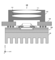
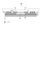
- 1 is a cross-sectional view showing a configuration example of a semiconductor device according to a first embodiment of the present technology
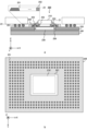
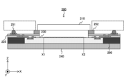
- 1A and 1B are a cross-sectional view and a plan view showing a configuration example of a semiconductor package according to a first embodiment of the present technology
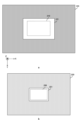
- 1 is an example of a plan view of a mounting board and a wiring board according to a first embodiment of the present technology
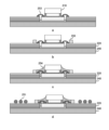
- 4A to 4C are diagrams for explaining a manufacturing method up to bonding of metal plates in the first embodiment of the present technology.
- 10A to 10C are diagrams for explaining a manufacturing method up to the formation of a dam in the first embodiment of the present technology.
- 5A to 5C are diagrams for explaining a manufacturing method up to the formation of an external terminal in the first embodiment of the present technology.
- FIG. 1A and 1B are a cross-sectional view and a plan view showing a configuration example of a semiconductor package according to a first modified example of the first embodiment of the present technology
- 11 is a cross-sectional view showing a case where a dust prevention wall in a first modified example of the first embodiment of the present technology is also used as a dam.
- FIG. FIG. 11 is a cross-sectional view showing an example of a semiconductor device in which the lens unit is tilted.
- 11A and 11B are a cross-sectional view and a plan view showing a configuration example of a semiconductor package according to a second modified example of the first embodiment of the present technology; 11A and 11B are a cross-sectional view and a plan view showing a configuration example of a semiconductor package according to a second embodiment of the present technology.
- 13A to 13C are diagrams for explaining a manufacturing method up to formation of a sealing material according to a second embodiment of the present technology.
- 13A to 13C are diagrams for explaining a manufacturing method up to the formation of external terminals according to a second embodiment of the present technology.
- 13A and 13B are a cross-sectional view and a plan view showing a configuration example of a semiconductor package according to a first modified example of the second embodiment of the present technology
- 13A and 13B are a cross-sectional view and a plan view showing a configuration example of a semiconductor package according to a second modified example of the second embodiment of the present technology
- 13A and 13B are a cross-sectional view and a plan view showing a configuration example of a semiconductor package according to a third modified example of the second embodiment of the present technology
- 13A and 13B are a cross-sectional view and a plan view showing a configuration example of a semiconductor package in which a dust prevention wall is eliminated in a third modified example of the second embodiment of the present technology
- 13A and 13B are a cross-sectional view and a plan view showing a configuration example of a semiconductor package according to a fourth modified example of the second embodiment of the present technology
- 13A and 13B are a cross-sectional view and a plan view showing a
- FIG. 13 is a cross-sectional view showing a configuration example of a semiconductor package according to a sixth modified example of the second embodiment of the present technology.
- 13A to 13C are diagrams for explaining a manufacturing method up to formation of a sealing material in a sixth modified example of the second embodiment of the present technology.
- 13A to 13C are diagrams for explaining a manufacturing method up to the formation of an external terminal in a sixth modified example of the second embodiment of the present technology.
- FIG. 13 is a cross-sectional view showing a configuration example of a semiconductor package according to a third embodiment of the present technology.
- 1 is a block diagram showing an example configuration of an electronic device according to an embodiment of the present technology;
- First embodiment example in which external terminals are provided on the upper surface of a wiring board
- Second embodiment an example in which the area of the transparent member is increased and external terminals are provided on the upper surface of the wiring board
- Third embodiment an example in which external terminals are provided on the upper surface of a wiring board and a semiconductor chip is connected by bumps
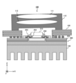
- First embodiment [Configuration example of semiconductor device] 1 is a cross-sectional view showing a configuration example of a semiconductor device 100 according to an embodiment of the present technology.
- the semiconductor device 100 is a device for capturing image data, and includes a lens module.
- a lens unit 110, a mounting substrate 120, a semiconductor package 200, and an external heat sink 130 are arranged in the lens module.
- Examples of the semiconductor device 100 include a smartphone, a digital still camera, and an in-vehicle camera.
- Lens unit 110 is a component that contains a predetermined number of lenses, such as lenses 111 and 112, and is mounted on mounting board 120. This lens unit 110 focuses incident light and guides it to semiconductor package 200.
- the optical axis of the lens unit 110 is referred to as the "Z axis," and a specific axis perpendicular to the Z axis is referred to as the "X axis.”
- the axis perpendicular to the X axis and Z axis is referred to as the "Y axis.” This figure shows a cross-sectional view seen from the Y axis direction.
- the mounting substrate 120 is a substrate on which the semiconductor package 200 is mounted, and is also called a motherboard.
- a through hole is formed in the mounting substrate 120, and light is incident on the light receiving surface of the semiconductor package 200 through this through hole.
- the light receiving surface will be referred to as the "upper surface” and the surface opposite the light receiving surface will be referred to as the "lower surface.”
- the space surrounded by the lower surface of the lens unit 110, the side surface of the mounting substrate 120, and the upper surface of the semiconductor package 200 will be referred to as the "cavity.”
- the semiconductor package 200 is a package that houses a semiconductor chip such as a solid-state imaging element.
- the configuration of the semiconductor package 200 will be described in detail later.
- the external heat sink 130 is connected to the underside of the semiconductor package 200 and dissipates heat generated by the semiconductor package 200.
- a metal member with a predetermined number of fins is used as the external heat sink 130.
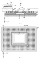
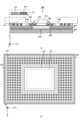
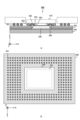
- [Example of semiconductor package configuration] 2 is a cross-sectional view and a plan view showing a configuration example of a semiconductor package 200 according to a first embodiment of the present technology.
- a shows a cross-sectional view of the semiconductor package 200 as viewed from the Y-axis direction.
- the thick dotted line in the figure a shows the outline of the mounting substrate 120.
- b shows a plan view of the semiconductor package 200 as viewed from the Z-axis direction.
- the semiconductor package 200 includes a transparent member 210, a wiring board 220, a semiconductor chip 230, and a metal plate 240.
- the area of the transparent member 210 is slightly smaller than the area of the semiconductor chip 230.
- the metal plate 240 is a metal substrate that dissipates heat generated by the semiconductor chip 230 and the wiring board 220.
- the rigidity and thermal conductivity of the metal plate 240 are higher than those of the mounting board 120, and the upper surface of the metal plate 240 is connected to the lower surface of the wiring board 220.
- the outer periphery of the metal plate 240 for example, approximately matches the outer periphery of the wiring board 220.
- “approximately matches” means a perfect match, or the difference is within an acceptable value.
- the wiring board 220 is a frame-shaped substrate for electrically connecting the semiconductor package 200 to the mounting board 120, and is also called an interposer.
- an organic substrate is used as the wiring board 220.
- the outer periphery of the wiring board 220 is rectangular when viewed from the Z-axis direction, and a rectangular through-hole 221 is formed in the center.
- the dotted line in b in the figure indicates the outer periphery of the transparent member 210.
- a predetermined number of external terminals 251 are arranged inside the outer periphery of the metal plate 240 when viewed from the Z-axis direction.
- solder balls are used as these external terminals 251.
- Each of the external terminals 251 is connected to the mounting board 120.
- pins can also be used as the external terminals 251.
- a package in which solder balls are arranged is also called a BGA (Ball Grid Array) package.
- a package in which pins are arranged is also called a PGA (Pin Grid Array) package.
- the semiconductor chip 230 is placed in the through hole 221 of the wiring board 220.
- the bottom surface of the semiconductor chip 230 is adhered to the top surface of the metal plate 240 exposed in the through hole 221 with an adhesive 256.
- the semiconductor chip 230 is electrically connected to the top surface of the wiring board 220 by a bonding wire 253.
- the bonding wire 253 is covered with a sealing material 254.
- a dam 255 is placed on the outside of the bonding wire 253.
- the semiconductor chip 230 may be a solid-state image sensor that captures image data by photoelectric conversion.
- a transparent member 210 is connected to the upper surface (light receiving surface) of the semiconductor chip 230 via a sealant 252.
- a resin or the like is used as the sealant 252.
- the transparent member 210 is a member that transmits incident light and protects the semiconductor chip 230, and is also called a cover glass or seal glass.
- the height Z1 of the upper surface of the transparent member 210 from the wiring board 220 is greater than the height of the external terminal 251 from the wiring board 220.
- the semiconductor package 200 When the semiconductor package 200 is observed from above, the semiconductor chip 230, the encapsulant 254, and the sealant 252 can actually be seen. However, in FIG. 1B, these are omitted for ease of illustration.
- the outer periphery of the sealing material 252 is equal to or smaller than the outer periphery of the transparent member 210, and for example, the outer peripheries are approximately the same. Therefore, as illustrated in b in the figure, when viewed from the Z-axis direction, the sealing material 252 hardly protrudes from the transparent member 210.
- the height Z2 of the sealant 252 from the wiring board 220 is slightly greater than the height of the external terminals 251 from the wiring board 220.
- the sealant 252 has a lower elastic modulus than the external terminals 251.
- a predetermined number of external terminals 251 are arranged on the upper surface (light-receiving surface) of the frame-shaped wiring board 220, and the semiconductor chip 230 is electrically connected to the upper surface of the wiring board 220 by bonding wires 253.
- the transparent member 210 is connected to the upper surface of the wiring board 220 via a sealing material 252.
- the metal plate 240 has higher rigidity and thermal conductivity than the mounting board 120, and is connected to the lower surface of the wiring board 220.
- a comparative example is considered in which the external terminals 251 are arranged on the underside of the wiring board 220.
- the outer periphery of the metal plate 240 needs to be smaller than the outer periphery of the wiring board 220, which restricts the area of the metal plate 240.
- the mounting board 120 can be compressed from above when mounting the mounting board 120, and peeling of the semiconductor package 200 from the mounting board 120 can be prevented.
- the size of the lens unit 110 (not shown) as viewed from the Z-axis direction can be made approximately the same as the semiconductor package 200. This makes it possible to realize a space-saving semiconductor device 100.
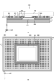
- FIG. 3 is an example of a plan view of the mounting substrate 120 and the wiring substrate 220 in the first embodiment of the present technology.
- a is an example of a plan view of the mounting substrate 120
- b is an example of a plan view of the wiring substrate 220.
- the outer periphery of the mounting substrate 120 is rectangular when viewed from the Z-axis direction, and a rectangular through-hole 121 is formed in the center.
- a transparent member 210 (not shown) is disposed within this through-hole 121.
- the dotted line in a in the figure indicates the outer periphery of the transparent member 210.
- the outer periphery of the wiring substrate 220 is rectangular when viewed from the Z-axis direction, and a rectangular through hole 221 is formed in the center.
- the semiconductor chip 230 (not shown) is disposed in this through hole 221.
- the dotted line in b of the figure indicates the outer periphery of the semiconductor chip 230.
- the outer periphery of the mounting substrate 120 is larger than the outer periphery of the wiring substrate 220, and the area of the through hole 121 is larger than the area of the through hole 221.
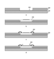
- a wiring board 220 is created.
- a film-like adhesive 222 is attached to the bottom surface of the wiring board 220.
- through holes are formed in the wiring board 220 by router processing or the like.
- a metal plate 240 is connected to the bottom surface of the wiring board 220 via the adhesive 222.
- a paste-like adhesive 256 is applied to the area of the upper surface of the metal plate 240 that is exposed from the through-hole of the wiring board 220.
- the semiconductor chip 230 is attached (in other words, die-bonded) to the upper surface of the metal plate 240.
- curing is performed, for example.
- the semiconductor chip 230 and the wiring board 220 are electrically connected by bonding wires 253.
- a sealant 252 is formed around the pixel region of the semiconductor chip 230.
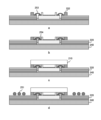
- the transparent member 210 is placed.
- a dam 255 is formed on the outside of the bonding wire 253.
- the dam 255 is formed, for example, by applying resin with a dispenser.
- the bonding wire 253 is covered with a sealing material 254.
- a predetermined number of external terminals 251 are formed on the upper surface of the wiring board 220.
- a predetermined number of external terminals 251 are arranged on the upper surface (i.e., the light receiving surface) of the wiring board 220, and the metal plate 240 is connected to the lower surface of the board, so that the area of the metal plate 240 can be made larger than in the comparative example. This can improve the heat dissipation properties of the semiconductor package 200.
- the semiconductor package 200 in the first modified example of the first embodiment differs from the first embodiment in that a dust prevention wall is formed between the sealing material 252 and the external terminals 251 to prevent the intrusion of dust.
- FIG. 7 is a cross-sectional view and a plan view showing an example of a configuration of a semiconductor package 200 in a first modified example of the first embodiment of the present technology.
- a shows a cross-sectional view of the semiconductor package 200 as viewed from the Y-axis direction.
- the thick dotted line in a shows the outline of the mounting board 120.
- b in the figure shows a plan view of the semiconductor package 200 as viewed from the Z-axis direction.
- the semiconductor package 200 in the first modified example of the first embodiment differs from the first embodiment in that a dust prevention wall 260 is formed between the external terminals 251 and the sealing material 252.
- This dust prevention wall 260 is formed along the inner periphery of the mounting board 120 (not shown) at its lower part. Furthermore, the height Z2 of the dust prevention wall 260 from the wiring board 220 is slightly greater than the height of the external terminal 251 from the wiring board 220. A material with a lower modulus of elasticity than the external terminal 251 (such as a rubber packing) is used as this dust prevention wall 260.
- the dust prevention wall 260 is an example of the first wall described in the claims.
- the dust prevention wall 260 is formed to surround the outer periphery of the transparent member 210. This dust prevention wall 260 prevents dust from entering the cavity.
- the dam 255 can be eliminated and the dust prevention wall 260 can function as a dam.
- a dust prevention wall 260 is formed between the sealing material 252 and the external terminal 251, so that it is possible to prevent dust from entering the cavity.
- the mounting substrate 120 is mounted on the top of the semiconductor package 200
- the lens unit 110 is mounted on the top of the mounting substrate 120.
- distortion may occur in the members inside the semiconductor package 200, and the optical axis of the lens unit 110 may deviate from the optical axis of the semiconductor package 200 as illustrated in Fig. 9.
- the semiconductor package 200 in the second modified example of the first embodiment differs from the first embodiment in that a stopper is formed along the outer periphery of the wiring substrate 220 to suppress deviation of the optical axis.
- FIG. 10 is a cross-sectional view and a plan view showing an example of a configuration of a semiconductor package 200 in a second modified example of the first embodiment of the present technology.
- a shows a cross-sectional view of the semiconductor package 200 as viewed from the Y-axis direction.
- the thick dotted line in a shows the outline of the mounting board 120.
- b in the figure shows a plan view of the semiconductor package 200 as viewed from the Z-axis direction.
- the second modified semiconductor package 200 of the first embodiment differs from the first embodiment in that a stopper 271 is formed on the upper surface of the wiring board 220 along its outer periphery.
- the height Z3 of the stopper 271 from the wiring board 220 is slightly smaller than the height of the external terminal 251 from the wiring board 220.
- the stopper 271 has a higher elasticity than the external terminal 251.
- the stopper 271 is an example of the first stopper described in the claims.
- the stopper 271 is formed around the outer periphery of the wiring board 220 so as to surround a large number of external terminals 251. In other words, the stopper 271 is disposed on the outside of the external terminals 251.
- stoppers 271 along the outer periphery of the wiring board 220, it is possible to suppress deviation of the optical axis and improve the accuracy of the optical axis.
- the stopper 271 is formed along the outer periphery of the wiring board 220, thereby improving the accuracy of the optical axis.
- the area of transparent member 210 is smaller than that of semiconductor chip 230, but this is not limited to the configuration.
- Semiconductor package 200 in the second embodiment differs from the first embodiment in that the area of transparent member 210 is larger than that of semiconductor chip 230.
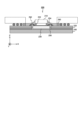
- FIG. 11 is a cross-sectional view showing an example of a configuration of a semiconductor package 200 in the second embodiment of the present technology. This figure shows a cross-sectional view of the semiconductor package 200 as seen from the Y-axis direction. The thick dotted line in this figure indicates the outline of the mounting substrate 120.
- the semiconductor package 200 in the second embodiment differs from the first embodiment in that the area of the transparent member 210 is larger than the area of the semiconductor chip 230.
- the sealing material 252 is disposed on the outside of the bonding wire 253, and the dam 255 is disposed on the inside of the bonding wire 253.
- a paste-like adhesive 256 is applied to the area of the upper surface of the metal plate 240 exposed from the through-hole of the wiring board 220.
- the semiconductor chip 230 is attached (in other words, die-bonded) to the upper surface of the metal plate 240.
- curing is performed, for example.
- the semiconductor chip 230 and the wiring board 220 are electrically connected by bonding wires 253.
- a dam 255 is formed around the pixel area of the semiconductor chip 230 to protect that area.
- the dam 255 is formed, for example, by applying resin with a dispenser.
- a sealant 252 is formed on the upper surface of the wiring board 220, outside the bonding wires 253. Then, as shown in FIG. 13B, the bonding wires 253 are covered with a sealing material 254. Then, as shown in FIG. 13C, the transparent member 210 is placed. Then, as shown in FIG. 13D, a predetermined number of external terminals 251 are formed on the upper surface of the wiring board 220.
- the area of the transparent member 210 is made larger than the semiconductor chip 230, so that the sealing material 252 can be formed on the upper surface of the wiring substrate 220.
- the outer periphery of the sealant 252 is the same as the outer periphery of the transparent member 210 when viewed from the Z-axis direction, but in this configuration, there is a risk of dust entering the cavity through gaps in the external terminals 251. If dust enters, the dust may adhere to the lenses in the lens unit 110 or the transparent member 210, causing a deterioration in the image quality of the image data.
- the semiconductor package 200 in the first modified example of the second embodiment differs from the second embodiment in that the outer periphery of the sealant 252 is made larger than the outer periphery of the transparent member 210 to prevent dust from entering.
- FIG. 14 is a cross-sectional view and a plan view showing an example of a configuration of a semiconductor package 200 in a first modified example of the second embodiment of the present technology.
- a shows a cross-sectional view of the semiconductor package 200 as viewed from the Y-axis direction.
- the thick dotted line in a shows the outline of the mounting board 120.
- b in the figure shows a plan view of the semiconductor package 200 as viewed from the Z-axis direction.
- the outer periphery of the sealing material 252 when viewed from the Z-axis direction, is larger than the outer periphery of the transparent member 210 and is equal to or larger than the outer periphery of the through hole of the wiring board 220.
- the coordinates of the left and right ends of the sealing material 252 in the X-axis direction are X1 and X6.
- the coordinates of the left and right ends of the through hole in the wiring board 220 are X2 and X4.
- the coordinates of the left and right ends of the transparent member 210 are X3 and X4.
- the distance from X1 to X6 is greater than the distance from X2 to X5.
- the distance from X2 to X5 is greater than the distance from X3 to X4.
- a portion of the sealing material 252 protrudes outside the transparent member 210 when viewed from the Z-axis direction.
- the sealing material 252 can also function as a barrier to prevent dust from entering.
- the outer periphery of the sealing material 252 is made larger than the outer periphery of the transparent member 210 when viewed in the Z-axis direction, thereby preventing dust from entering the cavity.
- the outer periphery of the sealing material 252 is the same as the outer periphery of the transparent member 210 when viewed from the Z-axis direction, but this configuration may cause dust to enter the cavity through gaps in the external terminals 251.
- the semiconductor package 200 in the second modified example of the second embodiment differs from the second embodiment in that a dust prevention wall is formed between the sealing material 252 and the external terminals 251 to prevent dust from entering.
- FIG. 15 is a cross-sectional view and a plan view showing an example of a configuration of a semiconductor package 200 in a second modified example of the second embodiment of the present technology.
- a shows a cross-sectional view of the semiconductor package 200 as viewed from the Y-axis direction.
- the thick dotted line in a shows the outline of the mounting board 120.
- b in the figure shows a plan view of the semiconductor package 200 as viewed from the Z-axis direction.
- the semiconductor package 200 of the third embodiment differs from the first embodiment in that a dust prevention wall 260 is formed between the external terminal 251 and the sealing material 252.
- the outer periphery of the sealing material 252 is the same as the outer periphery of the transparent member 210.
- This dust prevention wall 260 is formed along the inner periphery of the mounting board 120 (not shown) at its lower part. Furthermore, the height Z2 of the dust prevention wall 260 from the wiring board 220 is slightly greater than the height of the external terminal 251 from the wiring board 220. A material with a lower modulus of elasticity than the external terminal 251 (such as a rubber packing) is used as this dust prevention wall 260.
- the dust prevention wall 260 is an example of the first wall described in the claims.
- the dust prevention wall 260 is formed to surround the outer periphery of the transparent member 210. This dust prevention wall 260 prevents dust from entering the cavity. The dust prevention wall 260 can also prevent the sealing material 252 from flowing out into the area where the external terminals 251 are arranged.
- a dust prevention wall 260 is formed between the sealing material 252 and the external terminal 251, so that it is possible to prevent dust from entering the cavity.
- the mounting substrate 120 is mounted on the top of the semiconductor package 200, and the lens unit 110 is mounted on the top of the mounting substrate 120.
- the semiconductor package 200 in the third modification of the second embodiment differs from the second modification of the second embodiment in that a stopper is formed along the outer periphery of the wiring substrate 220 to suppress deviation of the optical axis.
- FIG. 16 is a cross-sectional view and a plan view showing an example of a configuration of a semiconductor package 200 in a third modified example of the second embodiment of the present technology.
- a shows a cross-sectional view of the semiconductor package 200 as viewed from the Y-axis direction.
- the thick dotted line in a shows the outline of the mounting board 120.
- b in the figure shows a plan view of the semiconductor package 200 as viewed from the Z-axis direction.
- the semiconductor package 200 of the third modified example of the second embodiment differs from the second modified example of the second embodiment in that a stopper 271 is formed on the upper surface of the wiring board 220 along its outer periphery.
- the height Z3 of the stopper 271 from the wiring board 220 is slightly smaller than the height of the external terminal 251 from the wiring board 220.
- the stopper 271 has a higher elasticity than the external terminal 251.
- the stopper 271 is an example of the first stopper described in the claims.
- the stopper 271 is formed around the outer periphery of the wiring board 220 so as to surround a large number of external terminals 251. In other words, the stopper 271 is disposed on the outside of the external terminals 251.
- stoppers 271 along the outer periphery of the wiring board 220, it is possible to suppress deviation of the optical axis and improve the accuracy of the optical axis.
- the dust prevention wall 260 can also be eliminated.
- the stopper 271 is formed along the outer periphery of the wiring board 220, thereby improving the accuracy of the optical axis.
- the stoppers 271 are disposed on the outside of the external terminals 251, but to further improve the accuracy of the optical axis, it is preferable to also dispose stoppers on the inside of the external terminals 251.
- the semiconductor package 200 in the fourth modified example of the second embodiment differs from the third modified example of the second embodiment in that stoppers are also disposed on the inside of the external terminals 251.
- FIG. 18 is a cross-sectional view and a plan view showing an example of a configuration of a semiconductor package 200 in a fourth modified example of the second embodiment of the present technology.
- a shows a cross-sectional view of the semiconductor package 200 as viewed from the Y-axis direction.
- the thick dotted line in a shows the outline of the mounting board 120.
- b in the figure shows a plan view of the semiconductor package 200 as viewed from the Z-axis direction.
- the semiconductor package 200 of the fourth modified example of the second embodiment differs from the third modified example of the second embodiment in that a stopper 272 is further formed between the sealing material 252 and the external terminal 251 on the upper surface of the wiring board 220.
- the stopper 272 is disposed on the outside of the dust prevention wall 260.
- the elastic modulus and height of the stopper 272 are similar to those of the stopper 271.
- the stopper 272 is an example of the second stopper described in the claims.
- the stopper 272 is formed between the dust prevention wall 260 and the external terminal 251 so as to surround the dust prevention wall 260 when viewed from the Z-axis direction.
- the accuracy of the optical axis can be further improved by forming a stopper 272 between the sealing material 252 and the external terminal 251.
- stoppers 271 and 272 are provided, it is also possible to provide only stopper 272. Also, while stopper 272 is formed on the outside of dust prevention wall 260, it is also possible to enlarge the outer periphery of dust prevention wall 260 and form stopper 272 on the inside.
- a stopper 272 is also formed between the sealing material 252 and the external terminal 251, so the accuracy of the optical axis can be further improved.
- the dust prevention wall 260 is formed on the lower part of the mounting substrate 120 to prevent the intrusion of dust and the outflow of the sealing material 252, but this configuration may cause the sealing material 252 to flow into the cavity.
- the semiconductor package 200 in the fifth modification of the second embodiment differs from the second modification of the second embodiment in that the sealing material outflow prevention wall prevents the sealing material 252 from flowing into the cavity.
- FIG. 19 is a cross-sectional view showing an example of a configuration of a semiconductor package 200 in a fifth modified example of the second embodiment of the present technology.
- a shows a cross-sectional view of the semiconductor package 200 as viewed from the Y-axis direction.
- the thick dotted line in a shows the outline of the mounting board 120.
- b in the figure shows a plan view of the semiconductor package 200 as viewed from the Z-axis direction.
- the semiconductor package 200 of the fifth modified example of the second embodiment differs from the second modified example of the second embodiment in that a sealant outflow prevention wall 280 is further formed on the outside of the sealant 252.
- the height of the sealant outflow prevention wall 280 from the wiring board 220 is equal to or greater than the height of the sealant 252 from the wiring board 220.
- the sealing material outflow prevention wall 280 is formed on the outside of the sealing material 252 (not shown) so as to surround it when viewed from the Z-axis direction.
- the sealing material outflow prevention wall 280 is an example of the second wall described in the claims.
- sealing material outflow prevention wall 280 on the outside of the sealing material 252, it is possible to prevent the sealing material 252 from outflowing into the cavity.
- the fifth variant of the second embodiment can also be applied to the second embodiment and its first, third, and fourth variants.
- a sealant outflow prevention wall 280 is formed on the outside of the sealant 252, so that the sealant 252 can be prevented from outflowing into the cavity.
- the bonding wires 253 are sealed, but the present invention is not limited to this configuration.
- the semiconductor package 200 in the sixth modified example of the second embodiment differs from the second embodiment in that the bonding wires 253 are not sealed.
- FIG. 20 is a cross-sectional view showing an example of a configuration of a semiconductor package 200 in a sixth modified example of the second embodiment of the present technology.
- the figure shows a cross-sectional view of the semiconductor package 200 as seen from the Y-axis direction.
- the thick dotted line in the figure indicates the outline of the mounting substrate 120.
- the semiconductor package 200 in the sixth modified example of the second embodiment differs from the first embodiment in that the bonding wires 253 are not sealed with the sealing material 254.
- a paste-like adhesive 256 is applied to the area of the upper surface of the metal plate 240 exposed from the through-hole of the wiring board 220.
- the semiconductor chip 230 is attached (in other words, die-bonded) to the upper surface of the metal plate 240.
- the semiconductor chip 230 and the wiring board 220 are electrically connected by the bonding wire 253.
- a sealant 252 is formed on the outer side of the bonding wire 253 on the upper surface of the wiring board 220.
- the transparent member 210 is placed. Then, as shown in FIG. 22B, a predetermined number of external terminals 251 are formed on the upper surface of the wiring board 220.
- the bonding wires 253 are not sealed, so that part of the manufacturing process can be eliminated.
- the semiconductor chip 230 is connected to the wiring substrate 220 by bonding wires, but it may be connected by bumps.
- the semiconductor package 200 in the third embodiment differs from the first embodiment in that the semiconductor chip 230 is connected by bumps.
- FIG. 23 is a cross-sectional view showing an example of a configuration of a semiconductor package 200 in a third embodiment of the present technology.
- the figure shows a cross-sectional view of the semiconductor package 200 as seen from the Y-axis direction.
- the thick dotted line in the figure indicates the outline of the mounting substrate 120.
- a frame-shaped wiring board 225 is used instead of the wiring board 220.
- the area of the top surface of the semiconductor chip 230 is larger than the area of the through-holes of the wiring board 225.
- the area of the top surface of the semiconductor chip 230 surrounding the pixel region is connected to the bottom surface of the wiring board 225 by bumps.
- X1 and X2 are the coordinates of the left and right ends of the pixel region.
- the package with the configuration illustrated in the figure is also called a fan-out package.
- the area of the metal plate 240 is larger than that of the semiconductor chip 230 and is approximately the same as that of the wiring board 225.
- the space between the wiring board 225 and the metal plate 240 is filled with a molding resin 290.
- the outer periphery of the sealing material 252 is larger than the outer periphery of the transparent member 210, as in the second embodiment.
- the semiconductor chip 230 is connected to the wiring board 225 by bumps, making wire bonding unnecessary.
- the semiconductor package 200 according to this technology can be applied to all electronic devices that use solid-state imaging elements in their image capture sections (photoelectric conversion sections), such as camera devices such as digital still cameras and video cameras, mobile terminal devices with imaging functions, and copiers that use solid-state imaging elements in their image reading sections.
- image capture sections photoelectric conversion sections
- camera devices such as digital still cameras and video cameras
- mobile terminal devices with imaging functions mobile terminal devices with imaging functions
- copiers that use solid-state imaging elements in their image reading sections.
- the camera device 300 as an electronic device includes an optical unit 302, a solid-state imaging device 301, a DSP (Digital Signal Processor) circuit 303 which is a camera signal processing circuit, a frame memory 304, a display unit 305, a recording unit 306, an operation unit 307, and a power supply unit 308.
- the DSP circuit 303, the frame memory 304, the display unit 305, the recording unit 306, the operation unit 307, and the power supply unit 308 are appropriately connected via connection lines 309 such as bus lines.
- the solid-state imaging device 301 is stored in one of the semiconductor packages 200 according to each of the above-mentioned embodiments.
- the optical unit 302 includes multiple lenses, takes in incident light (image light) from a subject, and forms an image on the imaging surface of the solid-state imaging device 301.
- the solid-state imaging device 301 converts the amount of incident light formed on the imaging surface by the optical unit 302 into an electrical signal on a pixel-by-pixel basis, and outputs the signal as a pixel signal.
- the display unit 305 is, for example, a panel-type display device such as a liquid crystal panel or an organic EL (Electro Luminescence) panel, and displays moving images or still images captured by the solid-state imaging device 301.
- the recording unit 306 records the moving images or still images captured by the solid-state imaging device 301 on a recording medium such as a hard disk or semiconductor memory.
- Operation unit 307 issues operation commands for the various functions of camera device 300 under user operation.
- Power supply unit 308 appropriately supplies various types of power to these devices as operating power sources for DSP circuit 303, frame memory 304, display unit 305, recording unit 306, and operation unit 307.
- the solid-state imaging device 301 can achieve good heat dissipation with a simple configuration.
- the present technology can also be configured as follows. (1) a frame-shaped wiring board having a predetermined number of external terminals disposed on a light receiving surface; a semiconductor chip electrically connected to the wiring board; a transparent member connected to the light receiving surface of the wiring board or the semiconductor chip via a sealant; a metal plate having higher rigidity and thermal conductivity than a mounting substrate connected to the external terminal, and connected to one of the two surfaces of the wiring substrate facing the light receiving surface. (2) The semiconductor package according to (1), wherein the outer periphery of the sealing material is larger than the outer periphery of the transparent member when viewed from a direction perpendicular to the light receiving surface.
- a height of the first wall from the wiring board is greater than a height of the external terminal from the wiring board;
- the semiconductor package according to (7), wherein the elastic modulus of the first wall is smaller than that of the external terminal.
- a height of the sealing material from the wiring board is greater than a height of the external terminal from the wiring board,
- the semiconductor package according to any one of (1) to (9), wherein the elastic modulus of the sealing material is smaller than that of the external terminals.
- (11) The semiconductor package according to any one of (1) to (10), wherein the height of the light receiving surface of the transparent member from the wiring board is greater than the height of the external terminals from the wiring board.
- a semiconductor device comprising: a wiring board having a predetermined number of external terminals arranged on a light-receiving surface; a semiconductor chip electrically connected to the wiring board; a transparent member connected to the light-receiving surface of the wiring board or the semiconductor chip via a sealing material; and a semiconductor package including a metal plate having a higher rigidity and thermal conductivity than the mounting board connected to the external terminals, and connected to one of both sides of the wiring board that faces the light-receiving surface.
Landscapes
- Solid State Image Pick-Up Elements (AREA)
Abstract
外部端子を設けた半導体パッケージにおいて、放熱性を向上させる。 半導体パッケージは、配線基板、半導体チップ、透明部材、および、メタル板を具備する。枠状の配線基板の受光面に所定数の外部端子が配置される。半導体チップは、配線基板に電気的に接続される。透明部材は、配線基板または半導体チップの受光面にシール材を介して接続される。メタル板は、外部端子に接続される実装基板よりも剛性および熱伝導率が高く、配線基板の両面のうち受光面に対向する面に接続される。
Description
本技術は、半導体パッケージに関する。詳しくは、半導体チップを設けた半導体パッケージ、半導体装置、および、半導体パッケージの製造方法に関する。
従来より、イメージセンサなどの半導体チップを保護する半導体パッケージでは、そのチップで生じた熱を放熱するために、金属製の部材が用いられることがある。例えば、枠状の枠基板のキャビディ内にイメージセンサを設け、枠状の上メタル部と板状の下メタル部とで枠基板を挟んで、上部にガラスを載置した半導体パッケージが提案されている(例えば、特許文献1参照。)。この半導体パッケージ内の下メタル部の外周は枠基板の外周より小さく、枠基板の下面において、枠基板の外周と下メタル部の外周との間の領域に、外部接続用の外部端子としてコネクタが配置される。
上述の従来技術では、上メタル部および下メタル部により、イメージセンサで生じた熱の放熱を図っている。しかしながら、上述の構造では、枠基板の下面に外部端子(コネクタなど)を配置する必要があるため、その外部端子により、下メタル部の面積が制約されてしまう。このため、下メタル部の面積を拡大することができず、放熱性の向上が困難である。
本技術はこのような状況に鑑みて生み出されたものであり、外部端子を設けた半導体パッケージにおいて、放熱性を向上させることを目的とする。
本技術は、上述の問題点を解消するためになされたものであり、その第1の側面は、受光面に所定数の外部端子が配置された枠状の配線基板と、上記配線基板に電気的に接続された半導体チップと、上記配線基板または上記半導体チップの上記受光面にシール材を介して接続された透明部材と、上記外部端子に接続される実装基板よりも剛性および熱伝導率が高く、上記配線基板の両面のうち上記受光面に対向する面に接続されたメタル板とを具備する半導体パッケージ、および、その製造方法である。これにより、放熱性が向上するという作用をもたらす。
また、この第1の側面において、上記受光面に垂直な方向から見てシール材の外周は、上記透明部材の外周よりも大きくてもよい。これにより、ダストの侵入が防止されるという作用をもたらす。
また、この第1の側面において、上記配線基板の外周と前記シール材との間に形成されるストッパーをさらに具備してもよい。これにより、光軸の精度が改善するという作用をもたらす。
また、この第1の側面において、上記ストッパーは、上記配線基板の外周に沿って形成される第1のストッパーを含むものであってもよい。これにより、光軸の精度が改善するという作用をもたらす。
また、この第1の側面において、上記ストッパーは、上記シール材と上記外部端子との間に形成される第2のストッパーを含むものであってもよい。これにより、光軸の精度が改善するという作用をもたらす。
また、この第1の側面において、上記ストッパーの上記配線基板からの高さは、上記外部端子の上記配線基板からの高さより小さく、上記ストッパーの弾性率は、上記外部端子よりも大きくてもよい。これにより、光軸の精度が改善するという作用をもたらす。
また、この第1の側面において、上記外部端子と上記シール材との間に形成された第1壁をさらに具備してもよい。これにより、ダストの侵入が防止されるという作用をもたらす。
また、この第1の側面において、上記第1壁の上記配線基板からの高さは、上記外部端子の上記配線基板からの高さより大きく、上記第1壁の弾性率は、上記外部端子より小さくてもよい。これにより、ダストの侵入が防止されるという作用をもたらす。
また、この第1の側面において、上記第1壁と上記シール材との間に形成された第2壁をさらに具備してもよい。これにより、シール材の流出が防止されるという作用をもたらす。
また、この第1の側面において、上記シール材の上記配線基板からの高さは、上記外部端子の上記配線基板からの高さよりも大きく、上記シール材の弾性率は、上記外部端子よりも小さくてもよい。これにより、ダストの侵入が防止されるという作用をもたらす。
また、この第1の側面において、上記透明部材の受光面の上記配線基板からの高さは、上記外部端子の上記配線基板からの高さよりも大きくてもよい。これにより、外部端子より高い透明部材に光が入射されるという作用をもたらす。
また、この第1の側面において、上記配線基板の受光面に垂直な方向から見て上記メタル板の外周の内側に上記外部端子が配置されてもよい。これにより、省スペースな半導体パッケージが実現されるという作用をもたらす。
また、この第1の側面において、上記実装基板には貫通孔が形成され、上記透明部材は、上記貫通孔に配置されてもよい。これにより、キャビティが形成されるという作用をもたらす。
また、この第1の側面において、上記外部端子は、半田ボールまたはピンであってもよい。これにより、半導体パッケージが実装基板に電気的に接続されるという作用をもたらす。
また、この第1の側面において、上記半導体チップと上記配線基板とを電気的に接続するボンディングワイヤと、上記ボンディングワイヤを覆う封止材とをさらに具備してもよい。これにより、ボンディングワイヤが保護されるという作用をもたらす。
また、この第1の側面において、上記半導体チップは、上記配線基板にバンプにより電気的に接続されてもよい。これにより、ボンディングワイヤが不要になるという作用をもたらす。
また、本技術の第2の側面は、実装基板と、上記実装基板にマウントされるレンズユニットと、受光面に所定数の外部端子が配置された配線基板と、上記配線基板に電気的に接続された半導体チップと、上記配線基板または上記半導体チップの受光面にシール材を介して接続された透明部材と、上記外部端子に接続される上記実装基板よりも剛性および熱伝導率が高く、上記配線基板の両面のうち上記受光面に対向する面に接続されたメタル板とを備える半導体パッケージとを具備する半導体装置である。これにより、半導体装置の放熱性が向上するという作用をもたらす。
また、この第2の側面において、外部放熱板をさらに具備し、上記メタル板の両面の一方は、上記配線基板に接続され、他方は、上記外部放熱板に接続されてもよい。これにより、半導体装置の放熱性が向上するという作用をもたらす。
以下、本技術を実施するための形態(以下、実施の形態と称する)について説明する。説明は以下の順序により行う。
1.第1の実施の形態(配線基板の上面に外部端子を設けた例)
2.第2の実施の形態(透明部材の面積を広くし、配線基板の上面に外部端子を設けた例)
3.第3の実施の形態(配線基板の上面に外部端子を設け、半導体チップをバンプにより接続した例)
4.電子機器の構成例
1.第1の実施の形態(配線基板の上面に外部端子を設けた例)
2.第2の実施の形態(透明部材の面積を広くし、配線基板の上面に外部端子を設けた例)
3.第3の実施の形態(配線基板の上面に外部端子を設け、半導体チップをバンプにより接続した例)
4.電子機器の構成例
<1.第1の実施の形態>
[半導体装置の構成例]
図1は、本技術の実施の形態における半導体装置100の一構成例を示す断面図である。この半導体装置100は、画像データを撮像する装置であり、レンズモジュールを備える。レンズモジュール内には、レンズユニット110、実装基板120、半導体パッケージ200および外部放熱板130が配置される。半導体装置100としては、スマートフォン、デジタルスチルカメラや車載カメラが挙げられる。
[半導体装置の構成例]
図1は、本技術の実施の形態における半導体装置100の一構成例を示す断面図である。この半導体装置100は、画像データを撮像する装置であり、レンズモジュールを備える。レンズモジュール内には、レンズユニット110、実装基板120、半導体パッケージ200および外部放熱板130が配置される。半導体装置100としては、スマートフォン、デジタルスチルカメラや車載カメラが挙げられる。
レンズユニット110は、レンズ111および112などの所定枚数のレンズを格納した部品であり、実装基板120にマウントされる。このレンズユニット110は、入射光を集光して半導体パッケージ200に導く。
以下、レンズユニット110の光軸を「Z軸」とし、そのZ軸に垂直な所定の軸を「X軸」とする。X軸およびZ軸に垂直な軸を「Y軸」とする。同図は、Y軸方向から見た断面図を示す。
実装基板120は、半導体パッケージ200が実装される基板であり、マザーボードとも呼ばれる。この実装基板120には貫通孔が形成され、この貫通孔を介して半導体パッケージ200の受光面に光が入射される。
以下、基板や層の両面のうち、受光面を「上面」とし、その受光面に対向する面を「下面」とする。また、レンズユニット110の下面と、実装基板120の側面と、半導体パッケージ200の上面とに囲まれた空間を以下、「キャビティ」と称する。
半導体パッケージ200は、固体撮像素子などの半導体チップが格納されたパッケージである。半導体パッケージ200の構成の詳細については後述する。
外部放熱板130は、半導体パッケージ200の下面に接続され、半導体パッケージ200で生じた熱を放熱するものである。外部放熱板130として、例えば、所定数のフィンが形成された金属製の部材が用いられる。
[半導体パッケージの構成例]
図2は、本技術の第1の実施の形態における半導体パッケージ200の一構成例を示す断面図および平面図である。同図におけるaは、Y軸方向から見た半導体パッケージ200の断面図を示す。同図におけるaの太い点線は、実装基板120の輪郭を示す。同図におけるbは、Z軸方向から見た半導体パッケージ200の平面図を示す。
図2は、本技術の第1の実施の形態における半導体パッケージ200の一構成例を示す断面図および平面図である。同図におけるaは、Y軸方向から見た半導体パッケージ200の断面図を示す。同図におけるaの太い点線は、実装基板120の輪郭を示す。同図におけるbは、Z軸方向から見た半導体パッケージ200の平面図を示す。
同図におけるaに例示するように、半導体パッケージ200は、透明部材210、配線基板220、半導体チップ230およびメタル板240を備える。透明部材210の面積は、半導体チップ230の面積より若干小さいものとする。
メタル板240は、半導体チップ230や配線基板220で生じた熱を放熱する金属製の基板である。このメタル板240の剛性および熱伝導率は、実装基板120よりも高く、メタル板240の上面が配線基板220の下面に接続される。また、メタル板240の外周は、例えば、配線基板220の外周と略一致する。ここで、「略一致」は、完全一致、または、差分が許容値以内であることを意味する。
配線基板220は、半導体パッケージ200を実装基板120に電気的に接続するための枠状の基板であり、インターポーザとも呼ばれる。配線基板220として、例えば有機基板が用いられる。
同図におけるbに例示するように、Z軸方向から見て配線基板220の外周は矩形であり、その中央部には、矩形の貫通孔221が形成されている。同図におけるbの点線は、透明部材210の外周を示す。
また、配線基板220の上面(すなわち、受光面)には、Z軸方向から見てメタル板240の外周の内側に、所定数の外部端子251が配置される。これらの外部端子251として、例えば、半田ボールが用いられる。外部端子251のそれぞれは、実装基板120に接続される。なお、ピンを外部端子251として用いることもできる。半田ボールを配列したパッケージは、BGA(Ball Grid Array)パッケージとも呼ばれる。また、ピンを配列したパッケージは、PGA(Pin Grid Array)パッケージとも呼ばれる。
同図におけるaに例示するように、半導体チップ230は、配線基板220の貫通孔221に配置される。この半導体チップ230の下面は、貫通孔221内に露出したメタル板240の上面に接着剤256により接着される。また、半導体チップ230は、ボンディングワイヤ253により、配線基板220の上面に電気的に接続される。このボンディングワイヤ253は、封止材254により覆われる。そのボンディングワイヤ253の外側にダム255が配置される。半導体チップ230として、光電変換により画像データを撮像する固体撮像素子などが用いられる。
また、半導体チップ230の上面(受光面)にはシール材252を介して透明部材210が接続される。シール材252として、樹脂などが用いられる。透明部材210は、入射光を透過するとともに、半導体チップ230を保護するための部材であり、カバーガラスやシールガラスとも呼ばれる。透明部材210の上面の、配線基板220からの高さZ1は、外部端子251の配線基板220からの高さよりも大きいものとする。
上方向から半導体パッケージ200を観察した場合、実際には、半導体チップ230、封止材254やシール材252を視認することができる。しかしながら、同図におけるbでは、記載の便宜上、それらを省略している。
シール材252の外周は、透明部材210の外周以下のサイズであり、例えば、それらの外周は略一致する。このため、同図におけるbに例示するように、Z軸方向から見て、シール材252が透明部材210から、はみ出ることは殆ど無い。
また、同図におけるaに例示するように、シール材252の配線基板220からの高さZ2は、外部端子251の配線基板220からの高さよりも、やや大きい。シール材252として、外部端子251より弾性率の低いものが用いられる。
上述したように、枠状の配線基板220の上面(受光面)に所定数の外部端子251が配置され、その配線基板220の上面に半導体チップ230がボンディングワイヤ253により電気的に接続される。また、透明部材210は、配線基板220の上面にシール材252を介して接続される。メタル板240は、実装基板120よりも剛性および熱伝導率が高く、配線基板220の下面に接続される。
ここで、外部端子251を配線基板220の下面に配置した構成を比較例として想定する。この比較例では、外部端子251を配置するために、メタル板240の外周を配線基板220の外周より小さくする必要があり、メタル板240の面積が制約されてしまう。
これに対して、同図におけるaおよびbに例示した半導体パッケージ200では、外部端子251を配線基板220の上面に配置するため、メタル板240の面積が制約されず、比較例よりも広くすることができる。これにより、比較例よりも放熱性を向上させることができる。
また、配線基板220の上面に外部端子251を配置することにより、実装基板120を実装する際に、上から実装基板120を圧縮することができ、半導体パッケージ200の実装基板120からの剥離を防止することができる。
また、配線基板220の上面に外部端子251を配置することにより、Z軸方向から見たレンズユニット110(不図示)のサイズを半導体パッケージ200とほぼ同等にすることができる。これにより、省スペースな半導体装置100を実現することができる。
図3は、本技術の第1の実施の形態における実装基板120および配線基板220の平面図の一例である。同図におけるaは、実装基板120の平面図の一例であり、同図におけるbは、配線基板220の平面図の一例である。
同図におけるaに例示するように、Z軸方向から見て実装基板120の外周は矩形であり、その中央部に矩形の貫通孔121が形成されている。この貫通孔121内に透明部材210(不図示)が配置される。同図におけるaの点線は、透明部材210の外周を示す。
また、同図におけるbに例示するようにZ軸方向から見て配線基板220の外周は矩形であり、その中央部に矩形の貫通孔221が形成されている。この貫通孔221内に半導体チップ230(不図示)が配置される。同図におけるbの点線は、半導体チップ230の外周を示す。
また、同図におけるaおよびbに例示するように、実装基板120の外周は、配線基板220の外周より大きく、貫通孔121の面積は、貫通孔221の面積よりも大きい。
[半導体パッケージの製造方法]
続いて、図4から図6を参照して、半導体パッケージ200の製造方法について説明する。
続いて、図4から図6を参照して、半導体パッケージ200の製造方法について説明する。
まず、図4におけるaに例示するように、配線基板220が作成される。そして、同図におけるbに例示するように、配線基板220の下面にフィルム状の接着剤222が貼り付けられる。そして、同図におけるcに例示するように、配線基板220に、ルーター加工などにより貫通孔が形成される。そして、配線基板220の下面にメタル板240が、接着剤222を介して接続される。このメタル板240の接続の際には、例えば、加圧とキュアリングとが行われる。
次に、図5におけるaに例示するように、メタル板240の上面のうち、配線基板220の貫通孔から露出した領域に、ペースト状の接着剤256が塗布される。そして、同図におけるbに例示するように、メタル板240の上面に半導体チップ230が接着(言い換えれば、ダイボンド)される。ダイボンドの際には、例えば、キュアリングが行われる。そして、同図におけるcに例示するように、ボンディングワイヤ253により、半導体チップ230と配線基板220とが電気的に接続される。そして、同図におけるdに例示するように、半導体チップ230のうち、画素領域の周囲に、シール材252が形成される。
次に、図6におけるaに例示するように、透明部材210が載置される。そして、同図におけるbに例示するようにボンディングワイヤ253の外側にダム255が形成される。ダム255は、例えば、ディスペンサにより樹脂を塗布することにより形成される。そして、同図におけるcに例示するように、封止材254によりボンディングワイヤ253が覆われる。そして、同図におけるdに例示するように、配線基板220の上面に所定数の外部端子251が形成される。
このように、本技術の第1の実施の形態によれば、配線基板220の上面(すなわち、受光面)に所定数の外部端子251を配置し、その基板の下面にメタル板240を接続したため、メタル板240の面積を比較例よりも広くすることができる。これにより、半導体パッケージ200の放熱性を向上させることができる。
[第1の変形例]
上述の第1の実施の形態では、外部端子251の隙間を介してキャビティ内にダストが侵入するおそれがある。この第1の実施の形態の第1の変形例における半導体パッケージ200は、シール材252と外部端子251との間にダスト防止壁を形成してダストの侵入を防止した点において第1の実施の形態と異なる。
上述の第1の実施の形態では、外部端子251の隙間を介してキャビティ内にダストが侵入するおそれがある。この第1の実施の形態の第1の変形例における半導体パッケージ200は、シール材252と外部端子251との間にダスト防止壁を形成してダストの侵入を防止した点において第1の実施の形態と異なる。
図7は、本技術の第1の実施の形態の第1の変形例における半導体パッケージ200の一構成例を示す断面図および平面図である。同図におけるaは、Y軸方向から見た半導体パッケージ200の断面図を示す。同図におけるaの太い点線は、実装基板120の輪郭を示す。同図におけるbは、Z軸方向から見た半導体パッケージ200の平面図を示す。
同図におけるaに例示するように、第1の実施の形態の第1の変形例における半導体パッケージ200は、外部端子251とシール材252との間にダスト防止壁260が形成される点において第1の実施の形態と異なる。
このダスト防止壁260は、実装基板120(不図示)の内周に沿って、その下部に形成される。また、ダスト防止壁260の配線基板220からの高さZ2は、外部端子251の配線基板220からの高さよりも、やや大きいものとする。このダスト防止壁260として、外部端子251より弾性率の低いもの(ゴムパッキンなど)が用いられる。なお、ダスト防止壁260は、特許請求の範囲に記載の第1壁の一例である。
同図におけるbに例示するように、ダスト防止壁260は、透明部材210の外周を囲むように形成される。このダスト防止壁260により、キャビティ内へのダストの侵入が防止される。
なお、図8に例示するように、第1の実施の形態の第1の変形例において、ダム255を削減して、ダスト防止壁260にダムの機能を持たせることもできる。
このように、本技術の第1の実施の形態の第1の変形例によれば、シール材252と外部端子251との間にダスト防止壁260を形成したため、キャビティ内へのダストの侵入を防止することができる。
[第2の変形例]
上述の第1の実施の形態では、半導体パッケージ200の上部に実装基板120を実装し、その上部にレンズユニット110をマウントしていた。しかしながら、この構成では、例えば、温度変化などの環境の変化により、半導体パッケージ200内の部材に歪が生じ、図9に例示するようにレンズユニット110の光軸が、半導体パッケージ200の光軸からずれてしまうおそれがある。この第1の実施の形態の第2の変形例における半導体パッケージ200は、配線基板220の外周に沿ってストッパーを形成して、光軸のずれを抑制した点において第1の実施の形態と異なる。
上述の第1の実施の形態では、半導体パッケージ200の上部に実装基板120を実装し、その上部にレンズユニット110をマウントしていた。しかしながら、この構成では、例えば、温度変化などの環境の変化により、半導体パッケージ200内の部材に歪が生じ、図9に例示するようにレンズユニット110の光軸が、半導体パッケージ200の光軸からずれてしまうおそれがある。この第1の実施の形態の第2の変形例における半導体パッケージ200は、配線基板220の外周に沿ってストッパーを形成して、光軸のずれを抑制した点において第1の実施の形態と異なる。
図10は、本技術の第1の実施の形態の第2の変形例における半導体パッケージ200の一構成例を示す断面図および平面図である。同図におけるaは、Y軸方向から見た半導体パッケージ200の断面図を示す。同図におけるaの太い点線は、実装基板120の輪郭を示す。同図におけるbは、Z軸方向から見た半導体パッケージ200の平面図を示す。
同図におけるaに例示するように、第1の実施の形態の第2の変形例半導体パッケージ200は、配線基板220の上面において、その外周に沿ってストッパー271が形成される点において第1の実施の形態と異なる。また、ストッパー271の配線基板220からの高さZ3は、外部端子251の配線基板220からの高さよりも、やや小さいものとする。このストッパー271として、外部端子251より弾性率の高いものが用いられる。なお、ストッパー271は、特許請求の範囲に記載の第1のストッパーの一例である。
同図におけるbに例示するように、ストッパー271は、配線基板220の外周に沿って、多数の外部端子251を囲むように形成される。言い換えれば、ストッパー271は、外部端子251の外側に配置される。
同図におけるaおよびbに例示するように、配線基板220の外周に沿ってストッパー271を形成することにより、光軸のずれを抑制し、光軸の精度を改善することができる。
このように、本技術の第1の実施の形態の第2の変形例によれば、配線基板220の外周に沿ってストッパー271を形成したため、光軸の精度を改善することができる。
<2.第2の実施の形態>
上述の第1の実施の形態では、透明部材210の面積を半導体チップ230よりも小さくいたが、この構成に限定されない。この第2の実施の形態における半導体パッケージ200は、透明部材210の面積を半導体チップ230よりも大きくした点において第1の実施の形態と異なる。
上述の第1の実施の形態では、透明部材210の面積を半導体チップ230よりも小さくいたが、この構成に限定されない。この第2の実施の形態における半導体パッケージ200は、透明部材210の面積を半導体チップ230よりも大きくした点において第1の実施の形態と異なる。
図11は、本技術の第2の実施の形態における半導体パッケージ200の一構成例を示す断面図である。同図は、Y軸方向から見た半導体パッケージ200の断面図を示す。同図における太い点線は、実装基板120の輪郭を示す。
第2の実施の形態における半導体パッケージ200は、透明部材210の面積が半導体チップ230よりも大きい点において第1の実施の形態と異なる。この場合、シール材252が、ボンディングワイヤ253の外側に配置され、ダム255は、ボンディングワイヤ253の内側に配置される。
続いて、図12および図13を参照して、第2の実施の形態における半導体パッケージ200の製造方法について説明する。第2の実施の形態において、メタル板240の貼り合わせまでの工程は、第1の実施の形態と同様である。
メタル板240の貼り合わせ後に、図12におけるaに例示するように、メタル板240の上面のうち、配線基板220の貫通孔から露出した領域に、ペースト状の接着剤256が塗布される。そして、同図におけるbに例示するように、メタル板240の上面に半導体チップ230が接着(言い換えれば、ダイボンド)される。ダイボンドの際には、例えば、キュアリングが行われる。そして、同図におけるcに例示するように、ボンディングワイヤ253により、半導体チップ230と配線基板220とが電気的に接続される。そして、同図におけるdに例示するように、半導体チップ230のうち、画素領域の周囲に、その領域を保護するためのダム255が形成される。ダム255は、例えば、ディスペンサにより樹脂を塗布することにより形成される。
次に、図13におけるaに例示するように、配線基板220の上面において、ボンディングワイヤ253の外側にシール材252が形成される。そして、同図におけるbに例示するように、封止材254によりボンディングワイヤ253が覆われる。そして、同図におけるcに例示するように、透明部材210が載置される。そして、同図におけるdに例示するように、配線基板220の上面に所定数の外部端子251が形成される。
このように、本技術の第2の実施の形態によれば、透明部材210の面積を半導体チップ230よりも大きくしたため、シール材252を配線基板220の上面に形成することができる。
[第1の変形例]
上述の第2の実施の形態では、Z軸方向から見て、シール材252の外周は、透明部材210の外周と同一であったが、この構成では、外部端子251の隙間を介してキャビティ内にダストが侵入するおそれがある。ダストが侵入すると、レンズユニット110内のレンズや透明部材210にダストが付着し、画像データの画質が低下することがある。この第2の実施の形態の第1の変形例における半導体パッケージ200は、シール材252の外周を透明部材210の外周よりも大きくしてダストの侵入を防止した点において第2の実施の形態と異なる。
上述の第2の実施の形態では、Z軸方向から見て、シール材252の外周は、透明部材210の外周と同一であったが、この構成では、外部端子251の隙間を介してキャビティ内にダストが侵入するおそれがある。ダストが侵入すると、レンズユニット110内のレンズや透明部材210にダストが付着し、画像データの画質が低下することがある。この第2の実施の形態の第1の変形例における半導体パッケージ200は、シール材252の外周を透明部材210の外周よりも大きくしてダストの侵入を防止した点において第2の実施の形態と異なる。
図14は、本技術の第2の実施の形態の第1の変形例における半導体パッケージ200の一構成例を示す断面図および平面図である。同図におけるaは、Y軸方向から見た半導体パッケージ200の断面図を示す。同図におけるaの太い点線は、実装基板120の輪郭を示す。同図におけるbは、Z軸方向から見た半導体パッケージ200の平面図を示す。
同図におけるaおよびbに例示するように、第2の実施の形態の第1の変形例において、Z軸方向から見て、シール材252の外周は、透明部材210の外周より大きく、配線基板220の貫通孔の外周以上である。
例えば、同図におけるaに例示するように、X軸方向において、シール材252の左端および右端の座標をX1およびX6とする。また、配線基板220(不図示)の貫通孔の左端および右端の座標をX2およびX4とする。透明部材210の左端および右端をX3およびX4とする。この場合、X1からX6までの距離は、X2からX5までの距離より大きい。また、X2からX5までの距離は、X3からX4までの距離より大きい。
同図におけるbに例示するように、Z軸方向から見てシール材252の一部は、透明部材210の外側にはみ出ている。
同図におけるaおよびbに例示したように、Z軸方向から見てシール材252の外周を透明部材210の外周よりも大きくすることにより、シール材252を、ダスト侵入に対する防止壁としても機能させることができる。
このように、本技術の第2の実施の形態の第1の変形例によれば、Z軸方向から見てシール材252の外周を透明部材210の外周よりも大きくしたため、キャビティ内へのダストの侵入を防止することができる。
[第2の変形例]
上述の第2の実施の形態では、Z軸方向から見て、シール材252の外周は、透明部材210の外周と同一であったが、この構成では、外部端子251の隙間を介してキャビティ内にダストが侵入するおそれがある。この第2の実施の形態の第2の変形例における半導体パッケージ200は、シール材252と外部端子251との間にダスト防止壁を形成してダストの侵入を防止した点において第2の実施の形態と異なる。
上述の第2の実施の形態では、Z軸方向から見て、シール材252の外周は、透明部材210の外周と同一であったが、この構成では、外部端子251の隙間を介してキャビティ内にダストが侵入するおそれがある。この第2の実施の形態の第2の変形例における半導体パッケージ200は、シール材252と外部端子251との間にダスト防止壁を形成してダストの侵入を防止した点において第2の実施の形態と異なる。
図15は、本技術の第2の実施の形態の第2の変形例における半導体パッケージ200の一構成例を示す断面図および平面図である。同図におけるaは、Y軸方向から見た半導体パッケージ200の断面図を示す。同図におけるaの太い点線は、実装基板120の輪郭を示す。同図におけるbは、Z軸方向から見た半導体パッケージ200の平面図を示す。
同図におけるaに例示するように、第3の実施の形態の半導体パッケージ200は、外部端子251とシール材252との間にダスト防止壁260が形成される点において第1の実施の形態と異なる。なお、シール材252の外周は、透明部材210の外周と同一である。
このダスト防止壁260は、実装基板120(不図示)の内周に沿って、その下部に形成される。また、ダスト防止壁260の配線基板220からの高さZ2は、外部端子251の配線基板220からの高さよりも、やや大きいものとする。このダスト防止壁260として、外部端子251より弾性率の低いもの(ゴムパッキンなど)が用いられる。なお、ダスト防止壁260は、特許請求の範囲に記載の第1壁の一例である。
同図におけるbに例示するように、ダスト防止壁260は、透明部材210の外周を囲むように形成される。このダスト防止壁260により、キャビティ内へのダストの侵入が防止される。また、ダスト防止壁260により、シール材252が、外部端子251の配列された領域に流れ出すことを防止することもできる。
このように、本技術の第2の実施の形態の第2の変形例によれば、シール材252と外部端子251との間にダスト防止壁260を形成したため、キャビティ内へのダストの侵入を防止することができる。
[第3の変形例]
上述の第2の実施の形態の第2の変形例では、半導体パッケージ200の上部に実装基板120を実装し、その上部にレンズユニット110をマウントしていた。しかしながら、この構成では、例えば、温度変化などの環境の変化により、半導体パッケージ200内の部材に歪が生じ、レンズユニット110の光軸が、半導体パッケージ200の光軸からずれてしまうおそれがある。この第2の実施の形態の第3の変形例における半導体パッケージ200は、配線基板220の外周に沿ってストッパーを形成して、光軸のずれを抑制した点において第2の実施の形態の第2の変形例と異なる。
上述の第2の実施の形態の第2の変形例では、半導体パッケージ200の上部に実装基板120を実装し、その上部にレンズユニット110をマウントしていた。しかしながら、この構成では、例えば、温度変化などの環境の変化により、半導体パッケージ200内の部材に歪が生じ、レンズユニット110の光軸が、半導体パッケージ200の光軸からずれてしまうおそれがある。この第2の実施の形態の第3の変形例における半導体パッケージ200は、配線基板220の外周に沿ってストッパーを形成して、光軸のずれを抑制した点において第2の実施の形態の第2の変形例と異なる。
図16は、本技術の第2の実施の形態の第3の変形例における半導体パッケージ200の一構成例を示す断面図および平面図である。同図におけるaは、Y軸方向から見た半導体パッケージ200の断面図を示す。同図におけるaの太い点線は、実装基板120の輪郭を示す。同図におけるbは、Z軸方向から見た半導体パッケージ200の平面図を示す。
同図におけるaに例示するように、第2の実施の形態の第3の変形例の半導体パッケージ200は、配線基板220の上面において、その外周に沿ってストッパー271が形成される点において第2の実施の形態の第2の変形例と異なる。また、ストッパー271の配線基板220からの高さZ3は、外部端子251の配線基板220からの高さよりも、やや小さいものとする。このストッパー271として、外部端子251より弾性率の高いものが用いられる。なお、ストッパー271は、特許請求の範囲に記載の第1のストッパーの一例である。
同図におけるbに例示するように、ストッパー271は、配線基板220の外周に沿って、多数の外部端子251を囲むように形成される。言い換えれば、ストッパー271は、外部端子251の外側に配置される。
同図におけるaおよびbに例示するように、配線基板220の外周に沿ってストッパー271を形成することにより、光軸のずれを抑制し、光軸の精度を改善することができる。
なお、図17に例示するように、第2の実施の形態の第3の変形例において、ダスト防止壁260を削減することもできる。
このように、本技術の第2の実施の形態の第3の変形例によれば、配線基板220の外周に沿ってストッパー271を形成したため、光軸の精度を改善することができる。
[第4の変形例]
上述の第2の実施の形態の第3の変形例では、外部端子251の外側にストッパー271を配置していたが、光軸の精度のさらなる改善のため、外部端子251の内側にもストッパーを配置することが好ましい。この第2の実施の形態の第4の変形例における半導体パッケージ200は、外部端子251の内側にもストッパーを配置した点において第2の実施の形態の第3の変形例と異なる。
上述の第2の実施の形態の第3の変形例では、外部端子251の外側にストッパー271を配置していたが、光軸の精度のさらなる改善のため、外部端子251の内側にもストッパーを配置することが好ましい。この第2の実施の形態の第4の変形例における半導体パッケージ200は、外部端子251の内側にもストッパーを配置した点において第2の実施の形態の第3の変形例と異なる。
図18は、本技術の第2の実施の形態の第4の変形例における半導体パッケージ200の一構成例を示す断面図および平面図である。同図におけるaは、Y軸方向から見た半導体パッケージ200の断面図を示す。同図におけるaの太い点線は、実装基板120の輪郭を示す。同図におけるbは、Z軸方向から見た半導体パッケージ200の平面図を示す。
同図におけるaに例示するように、第2の実施の形態の第4の変形例の半導体パッケージ200は、配線基板220の上面において、シール材252と外部端子251との間にストッパー272がさらに形成される点において第2の実施の形態の第3の変形例と異なる。例えば、ストッパー272は、ダスト防止壁260の外側に配置される。ストッパー272の弾性率や高さは、ストッパー271と同様である。なお、ストッパー272は、特許請求の範囲に記載の第2のストッパーの一例である。
同図におけるbに例示するように、Z軸方向から見てストッパー272は、ダスト防止壁260を囲むように、ダスト防止壁260と外部端子251との間に形成される。
同図におけるaおよびbに例示するように、シール材252と外部端子251との間もストッパー272を形成することにより、光軸の精度をさらに改善することができる。
なお、ストッパー271および272の両方を配置しているが、ストッパー272のみを配置することもできる。また、ストッパー272をダスト防止壁260の外側に形成しているが、ダスト防止壁260の外周を大きくして、その内側にストッパー272を形成することもできる。
このように、本技術の第2の実施の形態の第4の変形例によれば、シール材252と外部端子251との間にもストッパー272をさらに形成したため、光軸の精度をさらに改善することができる。
[第5の変形例]
上述の第2の実施の形態の第2の変形例では、実装基板120の下部にダスト防止壁260を形成して、ダストの侵入とシール材252の流出とを防止していたが、この構成では、キャビティ内にシール材252が流出するおそれがある。この第2の実施の形態の第5の変形例における半導体パッケージ200は、シール材流出防止壁により、シール材252のキャビティ内への流出を防止する点において第2の実施の形態の第2の変形例と異なる。
上述の第2の実施の形態の第2の変形例では、実装基板120の下部にダスト防止壁260を形成して、ダストの侵入とシール材252の流出とを防止していたが、この構成では、キャビティ内にシール材252が流出するおそれがある。この第2の実施の形態の第5の変形例における半導体パッケージ200は、シール材流出防止壁により、シール材252のキャビティ内への流出を防止する点において第2の実施の形態の第2の変形例と異なる。
図19は、本技術の第2の実施の形態の第5の変形例における半導体パッケージ200の一構成例を示す断面図である。同図におけるaは、Y軸方向から見た半導体パッケージ200の断面図を示す。同図におけるaの太い点線は、実装基板120の輪郭を示す。同図におけるbは、Z軸方向から見た半導体パッケージ200の平面図を示す。
同図におけるaに例示するように、第2の実施の形態の第5の変形例の半導体パッケージ200は、シール材252の外側にシール材流出防止壁280をさらに形成した点において第2の実施の形態の第2の変形例と異なる。シール材流出防止壁280の配線基板220からの高さは、シール材252の配線基板220からの高さ以上であるものとする。
同図におけるbに例示するように、Z軸方向から見てシール材流出防止壁280は、シール材252(不図示)を囲むように、その外側に形成される。なお、シール材流出防止壁280は、特許請求の範囲に記載の第2壁の一例である。
同図におけるaおよびbに例示するように、シール材252の外側にシール材流出防止壁280を形成することにより、シール材252のキャビティ内への流出を防止することができる。
なお、第2の実施の形態と、その第1、第3、第4の変形例とのそれぞれに第2の実施の形態の第5の変形例を適用することもできる。
このように、本技術の第2の実施の形態の第5の変形例によれば、シール材252の外側にシール材流出防止壁280を形成したため、シール材252のキャビティ内への流出を防止することができる。
[第6の変形例]
上述の第2の実施の形態では、ボンディングワイヤ253を封止していたが、この構成に限定されない。この第2の実施の形態の第6の変形例における半導体パッケージ200は、ボンディングワイヤ253が封止されない点において第2の実施の形態と異なる。
上述の第2の実施の形態では、ボンディングワイヤ253を封止していたが、この構成に限定されない。この第2の実施の形態の第6の変形例における半導体パッケージ200は、ボンディングワイヤ253が封止されない点において第2の実施の形態と異なる。
図20は、本技術の第2の実施の形態の第6の変形例における半導体パッケージ200の一構成例を示す断面図である。同図は、Y軸方向から見た半導体パッケージ200の断面図を示す。同図における太い点線は、実装基板120の輪郭を示す。
第2の実施の形態の第6の変形例における半導体パッケージ200は、ボンディングワイヤ253が封止材254により封止されない点において第1の実施の形態と異なる。
続いて、図21および図22を参照して、第2の実施の形態の第6の変形例における半導体パッケージ200の製造方法について説明する。第2の実施の形態の第6の変形例において、メタル板240の貼り合わせまでの工程は、第1の実施の形態と同様である。
メタル板240の貼り合わせ後に、図21におけるaに例示するように、メタル板240の上面のうち、配線基板220の貫通孔から露出した領域に、ペースト状の接着剤256が塗布される。そして、同図におけるbに例示するように、メタル板240の上面に半導体チップ230が接着(言い換えれば、ダイボンド)される。ダイボンドの際には、例えば、キュアリングが行われる。そして、同図におけるcに例示するように、ボンディングワイヤ253により、半導体チップ230と配線基板220とが電気的に接続される。そして、同図におけるaに例示するように、配線基板220の上面において、ボンディングワイヤ253の外側にシール材252が形成される。
次に、図22におけるaに例示するように、透明部材210が載置される。そして、同図におけるbに例示するように、配線基板220の上面に所定数の外部端子251が形成される。
このように、本技術の第2の実施の形態の第6の変形例によれば、ボンディングワイヤ253を封止しないため、製造工程の一部を削減することができる。
<3.第3の実施の形態>
上述の第1の実施の形態では、半導体チップ230を配線基板220にボンディングワイヤにより接続していたが、バンプにより接続することもできる。この第3の実施の形態における半導体パッケージ200は、半導体チップ230をバンプにより接続した点において第1の実施の形態と異なる。
上述の第1の実施の形態では、半導体チップ230を配線基板220にボンディングワイヤにより接続していたが、バンプにより接続することもできる。この第3の実施の形態における半導体パッケージ200は、半導体チップ230をバンプにより接続した点において第1の実施の形態と異なる。
図23は、本技術の第3の実施の形態における半導体パッケージ200の一構成例を示す断面図である。同図は、Y軸方向から見た半導体パッケージ200の断面図を示す。同図における太い点線は、実装基板120の輪郭を示す。
第3の実施の形態において配線基板220の代わりに枠状の配線基板225が用いられる。半導体チップ230の上面の面積は、配線基板225の貫通孔の面積より大きい。半導体チップ230の上面のうち画素領域の周囲の領域は、配線基板225の下面にバンプにより接続される。同図において、X1およびX2は、画素領域の左端および右端の座標である。同図に例示した構成のパッケージは、ファンアウトパッケージとも呼ばれる。
また、メタル板240の面積は、半導体チップ230より大きく、配線基板225と同程度である。配線基板225とメタル板240との間には、モールド樹脂290が充填される。
また、シール材252の外周は、第2の実施の形態と同様に透明部材210の外周より大きい。
同図に例示したように、半導体チップ230をバンプにより配線基板225に接続することにより、ワイヤボンディングの工程が不要になる。
このように、本技術の第3の実施の形態によれば、半導体チップ230をバンプにより配線基板225に接続したため、ワイヤボンディングが不要になる。
<4.電子機器の構成例>
上述した実施形態に係る固体撮像装置の電子機器への適用例について、図24を用いて説明する。
上述した実施形態に係る固体撮像装置の電子機器への適用例について、図24を用いて説明する。
本技術に係る半導体パッケージ200は、デジタルスチルカメラやビデオカメラ等のカメラ装置や、撮像機能を有する携帯端末装置や、画像読取部に固体撮像素子を用いる複写機など、画像取込部(光電変換部)に固体撮像素子を用いる電子機器全般に対して適用可能である。
図24に示すように、電子機器としてのカメラ装置300は、光学部302と、固体撮像装置301と、カメラ信号処理回路であるDSP(Digital Signal Processor)回路303と、フレームメモリ304と、表示部305と、記録部306と、操作部307と、電源部308とを備える。DSP回路303、フレームメモリ304、表示部305、記録部306、操作部307および電源部308は、バスライン等の接続線309を介して適宜接続されている。固体撮像装置301は、上述した各実施形態に係る半導体パッケージ200のいずれかに格納される。
光学部302は、複数のレンズを含み、被写体からの入射光(像光)を取り込んで固体撮像装置301の撮像面上に結像する。固体撮像装置301は、光学部302によって撮像面上に結像された入射光の光量を画素単位で電気信号に変換して画素信号として出力する。
表示部305は、例えば、液晶パネルや有機EL(Electro Luminescence)パネル等のパネル型表示装置からなり、固体撮像装置301で撮像された動画または静止画を表示する。記録部306は、固体撮像装置301で撮像された動画または静止画を、ハードディスクや半導体メモリ等の記録媒体に記録する。
操作部307は、ユーザによる操作の下に、カメラ装置300が持つ様々な機能について操作指令を発する。電源部308は、DSP回路303、フレームメモリ304、表示部305、記録部306および操作部307の動作電源となる各種の電源を、これら供給対象に対して適宜供給する。
以上のようなカメラ装置300によれば、固体撮像装置301に関し、簡単な構成により良好な放熱性を得ることができる。
なお、上述の実施の形態は本技術を具現化するための一例を示したものであり、実施の形態における事項と、特許請求の範囲における発明特定事項とはそれぞれ対応関係を有する。同様に、特許請求の範囲における発明特定事項と、これと同一名称を付した本技術の実施の形態における事項とはそれぞれ対応関係を有する。ただし、本技術は実施の形態に限定されるものではなく、その要旨を逸脱しない範囲において実施の形態に種々の変形を施すことにより具現化することができる。
なお、本明細書に記載された効果はあくまで例示であって、限定されるものではなく、また、他の効果があってもよい。
なお、本技術は以下のような構成もとることができる。
(1)受光面に所定数の外部端子が配置された枠状の配線基板と、
前記配線基板に電気的に接続された半導体チップと、
前記配線基板または前記半導体チップの前記受光面にシール材を介して接続された透明部材と、
前記外部端子に接続される実装基板よりも剛性および熱伝導率が高く、前記配線基板の両面のうち前記受光面に対向する面に接続されたメタル板と
を具備する半導体パッケージ。
(2)前記受光面に垂直な方向から見てシール材の外周は、前記透明部材の外周よりも大きい
前記(1)記載の半導体パッケージ。
(3)前記配線基板の外周と前記シール材との間に形成されるストッパーをさらに具備する
前記(1)または(2)に記載の半導体パッケージ。
(4)前記ストッパーは、前記配線基板の外周に沿って形成される第1のストッパーを含む
前記(3)記載の半導体パッケージ。
(5)前記ストッパーは、前記シール材と前記外部端子との間に形成される第2のストッパーを含む
前記(3)または(4)に記載の半導体パッケージ。
(6)前記ストッパーの前記配線基板からの高さは、前記外部端子の前記配線基板からの高さより小さく、
前記ストッパーの弾性率は、前記外部端子よりも大きい
前記(3)から(5)のいずれかに記載の半導体パッケージ。
(7)前記外部端子と前記シール材との間に形成された第1壁をさらに具備する
前記(1)から(6)のいずれかに記載の半導体パッケージ。
(8)前記第1壁の前記配線基板からの高さは、前記外部端子の前記配線基板からの高さより大きく、
前記第1壁の弾性率は、前記外部端子より小さい
前記(7)記載の半導体パッケージ。
(9)前記第1壁と前記シール材との間に形成された第2壁をさらに具備する
前記(7)または(8)に記載の半導体パッケージ。
(10)前記シール材の前記配線基板からの高さは、前記外部端子の前記配線基板からの高さよりも大きく、
前記シール材の弾性率は、前記外部端子よりも小さい
前記(1)から(9)のいずれかに記載の半導体パッケージ。
(11)前記透明部材の受光面の前記配線基板からの高さは、前記外部端子の前記配線基板からの高さよりも大きい
前記(1)から(10)のいずれかに記載の半導体パッケージ。
(12)前記配線基板の受光面に垂直な方向から見て前記メタル板の外周の内側に前記外部端子が配置される前記(1)から(11)のいずれかに記載の半導体パッケージ。
(13)前記実装基板には貫通孔が形成され、
前記透明部材は、前記貫通孔に配置される
前記(1)から(12)のいずれかに記載の半導体パッケージ。
(14)前記外部端子は、半田ボールまたはピンである
前記(1)から(13)のいずれかに記載の半導体パッケージ。
(15)前記半導体チップと前記配線基板とを電気的に接続するボンディングワイヤと、
前記ボンディングワイヤを覆う封止材と
をさらに具備する前記(1)から(14)のいずれかに記載の半導体パッケージ。
(16)前記半導体チップは、前記配線基板にバンプにより電気的に接続される
前記(1)記載の半導体パッケージ。
(17)実装基板と、
前記実装基板にマウントされるレンズユニットと、
受光面に所定数の外部端子が配置された配線基板と、前記配線基板に電気的に接続された半導体チップと、前記配線基板または前記半導体チップの受光面にシール材を介して接続された透明部材と、前記外部端子に接続される前記実装基板よりも剛性および熱伝導率が高く、前記配線基板の両面のうち前記受光面に対向する面に接続されたメタル板とを備える半導体パッケージと
を具備する半導体装置。
(18)外部放熱板をさらに具備し、
前記メタル板の両面の一方は、前記配線基板に接続され、他方は、前記外部放熱板に接続される
前記(17)記載の半導体装置。
(19)実装基板よりも剛性および熱伝導率が高く、枠状の配線基板の両面のうち前記受光面に対向する面にメタル板を接続する手順と、
前記配線基板に半導体チップを電気的に接続する手順と、
前記配線基板または前記半導体チップの前記受光面にシール材を介して透明部材を接続する手順と、
前記配線基板の前記受光面に所定数の外部端子を形成する手順と
を具備する半導体パッケージの製造方法。
(1)受光面に所定数の外部端子が配置された枠状の配線基板と、
前記配線基板に電気的に接続された半導体チップと、
前記配線基板または前記半導体チップの前記受光面にシール材を介して接続された透明部材と、
前記外部端子に接続される実装基板よりも剛性および熱伝導率が高く、前記配線基板の両面のうち前記受光面に対向する面に接続されたメタル板と
を具備する半導体パッケージ。
(2)前記受光面に垂直な方向から見てシール材の外周は、前記透明部材の外周よりも大きい
前記(1)記載の半導体パッケージ。
(3)前記配線基板の外周と前記シール材との間に形成されるストッパーをさらに具備する
前記(1)または(2)に記載の半導体パッケージ。
(4)前記ストッパーは、前記配線基板の外周に沿って形成される第1のストッパーを含む
前記(3)記載の半導体パッケージ。
(5)前記ストッパーは、前記シール材と前記外部端子との間に形成される第2のストッパーを含む
前記(3)または(4)に記載の半導体パッケージ。
(6)前記ストッパーの前記配線基板からの高さは、前記外部端子の前記配線基板からの高さより小さく、
前記ストッパーの弾性率は、前記外部端子よりも大きい
前記(3)から(5)のいずれかに記載の半導体パッケージ。
(7)前記外部端子と前記シール材との間に形成された第1壁をさらに具備する
前記(1)から(6)のいずれかに記載の半導体パッケージ。
(8)前記第1壁の前記配線基板からの高さは、前記外部端子の前記配線基板からの高さより大きく、
前記第1壁の弾性率は、前記外部端子より小さい
前記(7)記載の半導体パッケージ。
(9)前記第1壁と前記シール材との間に形成された第2壁をさらに具備する
前記(7)または(8)に記載の半導体パッケージ。
(10)前記シール材の前記配線基板からの高さは、前記外部端子の前記配線基板からの高さよりも大きく、
前記シール材の弾性率は、前記外部端子よりも小さい
前記(1)から(9)のいずれかに記載の半導体パッケージ。
(11)前記透明部材の受光面の前記配線基板からの高さは、前記外部端子の前記配線基板からの高さよりも大きい
前記(1)から(10)のいずれかに記載の半導体パッケージ。
(12)前記配線基板の受光面に垂直な方向から見て前記メタル板の外周の内側に前記外部端子が配置される前記(1)から(11)のいずれかに記載の半導体パッケージ。
(13)前記実装基板には貫通孔が形成され、
前記透明部材は、前記貫通孔に配置される
前記(1)から(12)のいずれかに記載の半導体パッケージ。
(14)前記外部端子は、半田ボールまたはピンである
前記(1)から(13)のいずれかに記載の半導体パッケージ。
(15)前記半導体チップと前記配線基板とを電気的に接続するボンディングワイヤと、
前記ボンディングワイヤを覆う封止材と
をさらに具備する前記(1)から(14)のいずれかに記載の半導体パッケージ。
(16)前記半導体チップは、前記配線基板にバンプにより電気的に接続される
前記(1)記載の半導体パッケージ。
(17)実装基板と、
前記実装基板にマウントされるレンズユニットと、
受光面に所定数の外部端子が配置された配線基板と、前記配線基板に電気的に接続された半導体チップと、前記配線基板または前記半導体チップの受光面にシール材を介して接続された透明部材と、前記外部端子に接続される前記実装基板よりも剛性および熱伝導率が高く、前記配線基板の両面のうち前記受光面に対向する面に接続されたメタル板とを備える半導体パッケージと
を具備する半導体装置。
(18)外部放熱板をさらに具備し、
前記メタル板の両面の一方は、前記配線基板に接続され、他方は、前記外部放熱板に接続される
前記(17)記載の半導体装置。
(19)実装基板よりも剛性および熱伝導率が高く、枠状の配線基板の両面のうち前記受光面に対向する面にメタル板を接続する手順と、
前記配線基板に半導体チップを電気的に接続する手順と、
前記配線基板または前記半導体チップの前記受光面にシール材を介して透明部材を接続する手順と、
前記配線基板の前記受光面に所定数の外部端子を形成する手順と
を具備する半導体パッケージの製造方法。
100 半導体装置
110 レンズユニット
111、112 レンズ
120 実装基板
121、221 貫通孔
130 外部放熱板
200 半導体パッケージ
210 透明部材
220、225 配線基板
222、256 接着剤
230 半導体チップ
240 メタル板
251 外部端子
252 シール材
253 ボンディングワイヤ
254 封止材
255 ダム
260 ダスト防止壁
271、272 ストッパー
280 シール材流出防止壁
290 モールド樹脂
300 カメラ装置
301 固体撮像装置
302 光学部
303 DSP回路
304 フレームメモリ
305 表示部
306 記録部
307 操作部
308 電源部
309 接続線
110 レンズユニット
111、112 レンズ
120 実装基板
121、221 貫通孔
130 外部放熱板
200 半導体パッケージ
210 透明部材
220、225 配線基板
222、256 接着剤
230 半導体チップ
240 メタル板
251 外部端子
252 シール材
253 ボンディングワイヤ
254 封止材
255 ダム
260 ダスト防止壁
271、272 ストッパー
280 シール材流出防止壁
290 モールド樹脂
300 カメラ装置
301 固体撮像装置
302 光学部
303 DSP回路
304 フレームメモリ
305 表示部
306 記録部
307 操作部
308 電源部
309 接続線
Claims (19)
- 受光面に所定数の外部端子が配置された枠状の配線基板と、
前記配線基板に電気的に接続された半導体チップと、
前記配線基板または前記半導体チップの前記受光面にシール材を介して接続された透明部材と、
前記外部端子に接続される実装基板よりも剛性および熱伝導率が高く、前記配線基板の両面のうち前記受光面に対向する面に接続されたメタル板と
を具備する半導体パッケージ。 - 前記受光面に垂直な方向から見てシール材の外周は、前記透明部材の外周よりも大きい
請求項1記載の半導体パッケージ。 - 前記配線基板の外周と前記シール材との間に形成されるストッパーをさらに具備する
請求項1記載の半導体パッケージ。 - 前記ストッパーは、前記配線基板の外周に沿って形成される第1のストッパーを含む
請求項3記載の半導体パッケージ。 - 前記ストッパーは、前記シール材と前記外部端子との間に形成される第2のストッパーを含む
請求項3記載の半導体パッケージ。 - 前記ストッパーの前記配線基板からの高さは、前記外部端子の前記配線基板からの高さより小さく、
前記ストッパーの弾性率は、前記外部端子よりも大きい
請求項3記載の半導体パッケージ。 - 前記外部端子と前記シール材との間に形成された第1壁をさらに具備する
請求項1記載の半導体パッケージ。 - 前記第1壁の前記配線基板からの高さは、前記外部端子の前記配線基板からの高さより大きく、
前記第1壁の弾性率は、前記外部端子より小さい
請求項7記載の半導体パッケージ。 - 前記第1壁と前記シール材との間に形成された第2壁をさらに具備する
請求項7記載の半導体パッケージ。 - 前記シール材の前記配線基板からの高さは、前記外部端子の前記配線基板からの高さよりも大きく、
前記シール材の弾性率は、前記外部端子よりも小さい
請求項1記載の半導体パッケージ。 - 前記透明部材の受光面の前記配線基板からの高さは、前記外部端子の前記配線基板からの高さよりも大きい
請求項1記載の半導体パッケージ。 - 前記配線基板の受光面に垂直な方向から見て前記メタル板の外周の内側に前記外部端子が配置される請求項1記載の半導体パッケージ。
- 前記実装基板には貫通孔が形成され、
前記透明部材は、前記貫通孔に配置される
請求項1記載の半導体パッケージ。 - 前記外部端子は、半田ボールまたはピンである
請求項1記載の半導体パッケージ。 - 前記半導体チップと前記配線基板とを電気的に接続するボンディングワイヤと、
前記ボンディングワイヤを覆う封止材と
をさらに具備する請求項1記載の半導体パッケージ。 - 前記半導体チップは、前記配線基板にバンプにより電気的に接続される
請求項1記載の半導体パッケージ。 - 実装基板と、
前記実装基板にマウントされるレンズユニットと、
受光面に所定数の外部端子が配置された配線基板と、前記配線基板に電気的に接続された半導体チップと、前記配線基板または前記半導体チップの受光面にシール材を介して接続された透明部材と、前記外部端子に接続される前記実装基板よりも剛性および熱伝導率が高く、前記配線基板の両面のうち前記受光面に対向する面に接続されたメタル板とを備える半導体パッケージと
を具備する半導体装置。 - 外部放熱板をさらに具備し、
前記メタル板の両面の一方は、前記配線基板に接続され、他方は、前記外部放熱板に接続される
請求項17記載の半導体装置。 - 実装基板よりも剛性および熱伝導率が高く、枠状の配線基板の両面のうち前記受光面に対向する面にメタル板を接続する手順と、
前記配線基板に半導体チップを電気的に接続する手順と、
前記配線基板または前記半導体チップの前記受光面にシール材を介して透明部材を接続する手順と、
前記配線基板の前記受光面に所定数の外部端子を形成する手順と
を具備する半導体パッケージの製造方法。
Applications Claiming Priority (2)
| Application Number | Priority Date | Filing Date | Title |
|---|---|---|---|
| JP2023-192728 | 2023-11-13 | ||
| JP2023192728 | 2023-11-13 |
Publications (1)
| Publication Number | Publication Date |
|---|---|
| WO2025105035A1 true WO2025105035A1 (ja) | 2025-05-22 |
Family
ID=95742214
Family Applications (1)
| Application Number | Title | Priority Date | Filing Date |
|---|---|---|---|
| PCT/JP2024/033197 Pending WO2025105035A1 (ja) | 2023-11-13 | 2024-09-18 | 半導体パッケージ、半導体装置、および、半導体パッケージの製造方法 |
Country Status (1)
| Country | Link |
|---|---|
| WO (1) | WO2025105035A1 (ja) |
Citations (8)
| Publication number | Priority date | Publication date | Assignee | Title |
|---|---|---|---|---|
| JP2000299330A (ja) * | 1999-04-14 | 2000-10-24 | Matsushita Electric Ind Co Ltd | ベアチップ実装基板、ベアチップ実装方法及びベアチップ実装装置 |
| JP2004247611A (ja) * | 2003-02-14 | 2004-09-02 | Matsushita Electric Works Ltd | 半導体素子実装基板、半導体素子実装基板の製造方法 |
| JP2010252307A (ja) * | 2009-03-25 | 2010-11-04 | Kyocera Corp | 撮像装置および撮像モジュール |
| WO2011080952A1 (ja) * | 2009-12-28 | 2011-07-07 | 三洋電機株式会社 | 素子搭載用基板、半導体モジュール、カメラモジュールおよび素子搭載用基板の製造方法 |
| WO2013118501A1 (ja) * | 2012-02-07 | 2013-08-15 | 株式会社ニコン | 撮像ユニットおよび撮像装置 |
| JP2016122978A (ja) * | 2014-12-25 | 2016-07-07 | 京セラ株式会社 | 電子素子実装用基板および電子装置 |
| WO2020183881A1 (ja) * | 2019-03-12 | 2020-09-17 | ソニーセミコンダクタソリューションズ株式会社 | 半導体装置 |
| WO2021200094A1 (ja) * | 2020-03-31 | 2021-10-07 | ソニーセミコンダクタソリューションズ株式会社 | 半導体装置 |
-
2024
- 2024-09-18 WO PCT/JP2024/033197 patent/WO2025105035A1/ja active Pending
Patent Citations (8)
| Publication number | Priority date | Publication date | Assignee | Title |
|---|---|---|---|---|
| JP2000299330A (ja) * | 1999-04-14 | 2000-10-24 | Matsushita Electric Ind Co Ltd | ベアチップ実装基板、ベアチップ実装方法及びベアチップ実装装置 |
| JP2004247611A (ja) * | 2003-02-14 | 2004-09-02 | Matsushita Electric Works Ltd | 半導体素子実装基板、半導体素子実装基板の製造方法 |
| JP2010252307A (ja) * | 2009-03-25 | 2010-11-04 | Kyocera Corp | 撮像装置および撮像モジュール |
| WO2011080952A1 (ja) * | 2009-12-28 | 2011-07-07 | 三洋電機株式会社 | 素子搭載用基板、半導体モジュール、カメラモジュールおよび素子搭載用基板の製造方法 |
| WO2013118501A1 (ja) * | 2012-02-07 | 2013-08-15 | 株式会社ニコン | 撮像ユニットおよび撮像装置 |
| JP2016122978A (ja) * | 2014-12-25 | 2016-07-07 | 京セラ株式会社 | 電子素子実装用基板および電子装置 |
| WO2020183881A1 (ja) * | 2019-03-12 | 2020-09-17 | ソニーセミコンダクタソリューションズ株式会社 | 半導体装置 |
| WO2021200094A1 (ja) * | 2020-03-31 | 2021-10-07 | ソニーセミコンダクタソリューションズ株式会社 | 半導体装置 |
Similar Documents
| Publication | Publication Date | Title |
|---|---|---|
| KR101902731B1 (ko) | 반도체 장치 및 그 제조 방법 및 전자 기기 | |
| CN103915393B (zh) | 光电封装体及其制造方法 | |
| US9966401B2 (en) | Package for image sensor with outer and inner frames | |
| US7796188B2 (en) | Compact image sensor package and method of manufacturing the same | |
| US9019421B2 (en) | Method of manufacturing a miniaturization image capturing module | |
| US20140168510A1 (en) | Imaging element module and method for manufacturing the same | |
| JP7414720B2 (ja) | 半導体装置、電子機器、および半導体装置の製造方法 | |
| CN107845653B (zh) | 影像传感芯片的封装结构及封装方法 | |
| JP7372256B2 (ja) | 固体撮像装置および電子機器 | |
| WO2022156032A1 (zh) | 感光芯片及封装结构与其制造方法、摄像模组和电子设备 | |
| US20250160012A1 (en) | Semiconductor device, electronic device, and manufacturing method for semiconductor device | |
| US20070152345A1 (en) | Stacked chip packaging structure | |
| US7372135B2 (en) | Multi-chip image sensor module | |
| WO2022259684A1 (ja) | 固体撮像装置および電子機器 | |
| JP4466552B2 (ja) | 固体撮像装置の製造方法 | |
| WO2025105035A1 (ja) | 半導体パッケージ、半導体装置、および、半導体パッケージの製造方法 | |
| JP6990317B2 (ja) | 撮像ユニット及び撮像装置 | |
| JP7853279B2 (ja) | 半導体装置、半導体装置の製造方法及び電子機器 | |
| JP2013085095A (ja) | 撮像デバイス | |
| CN101521185A (zh) | 光学晶片的封装结构及封装制程 | |
| CN117059677A (zh) | 影像感测模组、显示模组及电子设备 | |
| CN116490967A (zh) | 成像装置、电子设备和成像装置的制造方法 | |
| KR20030088887A (ko) | 소형의 이미지 감지 및 처리 모듈과 그것의 제조 방법 | |
| US20250006755A1 (en) | Semiconductor device and electronic equipment | |
| KR20250133688A (ko) | 촬상 장치, 전자 기기 |
Legal Events
| Date | Code | Title | Description |
|---|---|---|---|
| 121 | Ep: the epo has been informed by wipo that ep was designated in this application |
Ref document number: 24891077 Country of ref document: EP Kind code of ref document: A1 |
|
| ENP | Entry into the national phase |
Ref document number: 2025557674 Country of ref document: JP Kind code of ref document: A |
|
| WWE | Wipo information: entry into national phase |
Ref document number: 2025557674 Country of ref document: JP |