WO2025100355A1 - 半導体装置、半導体装置の製造方法、および車両 - Google Patents
半導体装置、半導体装置の製造方法、および車両 Download PDFInfo
- Publication number
- WO2025100355A1 WO2025100355A1 PCT/JP2024/039059 JP2024039059W WO2025100355A1 WO 2025100355 A1 WO2025100355 A1 WO 2025100355A1 JP 2024039059 W JP2024039059 W JP 2024039059W WO 2025100355 A1 WO2025100355 A1 WO 2025100355A1
- Authority
- WO
- WIPO (PCT)
- Prior art keywords
- terminal
- semiconductor device
- electrode
- heat dissipation
- semiconductor
- Prior art date
- Legal status (The legal status is an assumption and is not a legal conclusion. Google has not performed a legal analysis and makes no representation as to the accuracy of the status listed.)
- Pending
Links
Images















Classifications
-
- H—ELECTRICITY
- H10—SEMICONDUCTOR DEVICES; ELECTRIC SOLID-STATE DEVICES NOT OTHERWISE PROVIDED FOR
- H10W—GENERIC PACKAGES, INTERCONNECTIONS, CONNECTORS OR OTHER CONSTRUCTIONAL DETAILS OF DEVICES COVERED BY CLASS H10
- H10W40/00—Arrangements for thermal protection or thermal control
- H10W40/40—Arrangements for thermal protection or thermal control involving heat exchange by flowing fluids
- H10W40/47—Arrangements for thermal protection or thermal control involving heat exchange by flowing fluids by flowing liquids, e.g. forced water cooling
-
- H—ELECTRICITY
- H10—SEMICONDUCTOR DEVICES; ELECTRIC SOLID-STATE DEVICES NOT OTHERWISE PROVIDED FOR
- H10W—GENERIC PACKAGES, INTERCONNECTIONS, CONNECTORS OR OTHER CONSTRUCTIONAL DETAILS OF DEVICES COVERED BY CLASS H10
- H10W90/00—Package configurations
Definitions
- This disclosure relates to a semiconductor device and a manufacturing method thereof, and a vehicle equipped with the semiconductor device.
- Patent Document 1 discloses an example of a semiconductor module that includes a semiconductor device and a cooler.
- the cooler includes a housing having a hollow region and a heat sink.
- the housing has an opening that leads to the hollow region.
- the heat sink is attached to the housing so as to cover the opening.
- a part of the heat sink is contained in the hollow region.
- the semiconductor device is joined to a part of the heat sink that protrudes from the hollow region. When a coolant (such as cooling water) is flowed through the hollow region, the coolant comes into contact with the heat sink. This allows the semiconductor device to be efficiently cooled via the heat sink.
- a coolant such as cooling water
- An object of the present disclosure is to provide a semiconductor device that is improved over conventional semiconductor devices.
- an object of the present disclosure is to provide a semiconductor device that can further improve cooling efficiency.
- the semiconductor device provided by the first aspect of the present disclosure includes a first semiconductor element having a first electrode located on one side in a first direction, a first terminal facing the first electrode, a first heat dissipation member electrically connected to the first terminal and conducting to the first electrode, and a first protective layer that covers a portion of the first semiconductor element and is an insulator.
- a first flow path is provided between the first semiconductor element and the first terminal.
- the first heat dissipation member is housed in the first flow path.
- the first protective layer is provided with a first opening through which the first electrode is exposed.
- the first heat dissipation member has a first end inserted into the first opening. A gap is provided between the first end and the first protective layer in the first opening.
- a method for manufacturing a semiconductor device includes a first step of conductively joining a first heat dissipation member to one side of a first terminal in a first direction, a second step of conductively joining a first semiconductor element to a second terminal, a third step of forming a first protective layer that covers a portion of the first semiconductor element and is an insulator, and a fourth step of conducting the first heat dissipation member to the first semiconductor element.
- the first semiconductor element has a first electrode located on the side opposite to the side facing the second terminal in the first direction.
- the first heat dissipation member has a first end located on the side opposite to the side facing the first terminal in the first direction.
- a first opening through which the first electrode is exposed is provided in the first protective layer.
- the first heat dissipation member is conducted to the first electrode by inserting the first end into the first opening.
- a first flow path is provided that is located between the first semiconductor element and the first terminal in the first direction and that accommodates the first heat dissipation member.
- a gap is provided between the first end and the first protective layer in the first opening.
- the vehicle provided by the third aspect of the present disclosure includes a drive source and a semiconductor device.
- the semiconductor device is electrically connected to the drive source.
- the semiconductor device further includes a second terminal compared to the semiconductor device provided by the first aspect of the present disclosure.
- the second terminal is located on the opposite side of the first terminal of the semiconductor device with respect to a first semiconductor element of the semiconductor device.
- the first semiconductor element has a second electrode that is electrically connected to the second terminal.
- the second electrode is located on the opposite side of the first electrode of the first semiconductor element in the first direction.
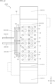
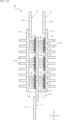
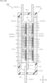
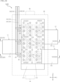
- FIG. 1 is a plan view of a semiconductor device according to a first embodiment of the present disclosure.
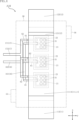
- FIG. 2 is a plan view corresponding to FIG. 1, seen through the housing.
- FIG. 3 is a plan view corresponding to FIG. 2, in which the third terminal and the plurality of fourth heat dissipation members are omitted.
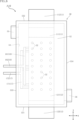
- FIG. 4 is a plan view corresponding to FIG. 3, and omits the third signal terminal, the fourth signal terminal, the plurality of second semiconductor elements, the plurality of second protective layers, the plurality of third heat dissipation members, the plurality of second gate pillars, the plurality of second detection pillars, the plurality of third leads, and the plurality of fourth leads.
- FIG. 5 is a plan view corresponding to FIG.
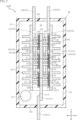
- FIG. 6 is a bottom view of the semiconductor device shown in FIG.
- FIG. 7 is a cross-sectional view taken along line VII-VII in FIG.
- FIG. 8 is a cross-sectional view taken along line VIII-VIII in FIG.
- FIG. 9 is a cross-sectional view taken along line IX-IX in FIG.
- FIG. 10 is a partially enlarged view of FIG.
- FIG. 11 is a partially enlarged view of FIG. 8, showing one of the plurality of first semiconductor elements and its vicinity.
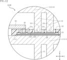
- FIG. 12 is a partially enlarged view of FIG. 8, showing one of the plurality of second semiconductor elements and its vicinity.
- FIG. 13 is a cross-sectional view showing a state in which a coolant flows downward in the semiconductor device shown in FIG.
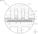
- FIG. 14 is a partially enlarged cross-sectional view of a semiconductor device according to a modified example of the first embodiment of the present disclosure.
- FIG. 15 is a cross-sectional view illustrating a first step in the manufacturing process of the semiconductor device shown in FIG.
- FIG. 16 is a cross-sectional view illustrating a second step in the manufacturing process of the semiconductor device shown in FIG.
- FIG. 17 is a cross-sectional view illustrating a third step in the manufacturing process of the semiconductor device shown in FIG.
- FIG. 18 is a cross-sectional view illustrating a fourth step in the manufacturing process of the semiconductor device shown in FIG.
- FIG. 19 is a schematic diagram of a vehicle on which the semiconductor device shown in FIG. 1 is mounted.
- FIG. 15 is a cross-sectional view illustrating a first step in the manufacturing process of the semiconductor device shown in FIG.
- FIG. 16 is a cross-sectional view illustrating a second step in the manufacturing process of the semiconductor device shown in FIG.
- FIG. 17 is
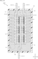
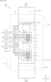
- FIG. 20 is a plan view of a semiconductor device according to a second embodiment of the present disclosure and corresponds to FIG.
- FIG. 21 is a plan view of the semiconductor device shown in FIG. 20 and corresponds to FIG.
- FIG. 22 is a cross-sectional view taken along line XXII-XXII in FIG.
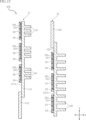
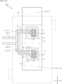
- FIG. 23 is a plan view of a semiconductor device according to a third embodiment of the present disclosure, and corresponds to FIG.
- FIG. 24 is a plan view of the semiconductor device shown in FIG. 23 and corresponds to FIG.
- FIG. 25 is a cross-sectional view taken along line XXV-XXV in FIG.
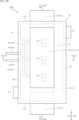
- FIG. 26 is a plan view of a semiconductor device according to a fourth embodiment of the present disclosure.
- FIG. 27 is a bottom view of the semiconductor device shown in FIG. 26.
- FIG. FIG. 28 is a cross-sectional view taken along line XXVIII-XXVIII in FIG.
- FIG. 29 is a cross-sectional view taken along line XXIX-XXIX in FIG.
- FIG. 30 is a plan view of a semiconductor device according to a fifth embodiment of the present disclosure.
- FIG. 31 is a plan view of the semiconductor device shown in FIG. 30 and corresponds to FIG.
- FIG. 32 is a plan view of the semiconductor device shown in FIG. 30 and corresponds to FIG.
- FIG. 33 is a plan view of the semiconductor device shown in FIG. 30 and corresponds to FIG.
- FIG. 34 is a cross-sectional view taken along line XXXIV-XXXIV in FIG.
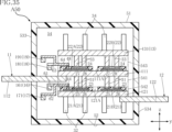
- FIG. 35 is a cross-sectional view taken along line XXXV-XXXV in FIG.
- a semiconductor device A10 according to a first embodiment of the present disclosure will be described with reference to FIGS. 1 to 13.
- the semiconductor device A10 is generally used in a power conversion circuit such as an inverter.
- the semiconductor device A10 includes a first terminal 11, a second terminal 12, a third terminal 13, a plurality of first semiconductor elements 21, a plurality of second semiconductor elements 22, a plurality of first protective layers 23, a plurality of second protective layers 24, a plurality of first heat dissipation members 31, a plurality of second heat dissipation members 32, a plurality of third heat dissipation members 33, a plurality of fourth heat dissipation members 34, and a housing 50.
- the semiconductor device A10 includes a first bonding layer 25, a second bonding layer 26, a third bonding layer 27, a fourth bonding layer 28, a fifth bonding layer 29, a plurality of first gate pillars 43, a plurality of first detection pillars 44, a plurality of second gate pillars 47, and a plurality of second detection pillars 48.
- the semiconductor device A10 further includes a first signal terminal 16, a second signal terminal 17, a third signal terminal 18, a fourth signal terminal 19, a plurality of first leads 61, a plurality of second leads 62, a plurality of third leads 63, and a plurality of fourth leads 64.
- FIGS. 2 to 5 show the housing 50 in a see-through manner. In FIGS.
- the see-through housing 50 is shown by an imaginary line (two-dot chain line).
- the third terminal 13 and the plurality of fourth heat dissipation members 34 are omitted from FIG. 2.
- the third signal terminal 18, the fourth signal terminal 19, the plurality of second semiconductor elements 22, the plurality of second protective layers 24, the plurality of third heat dissipation members 33, the plurality of second gate pillars 47, the plurality of second detection pillars 48, the plurality of third leads 63, and the plurality of fourth leads 64 are omitted from FIG. 3.
- the first terminal 11 is omitted in FIG. 5 compared to FIG.
- first direction z the normal direction of the first mounting surface 121A of the second terminal 12 described later is referred to as the "first direction z.”
- second direction x The direction perpendicular to both the first direction z and the second direction x is referred to as the "third direction y.”
- a half-bridge circuit is configured that includes a plurality of first semiconductor elements 21 and a plurality of second semiconductor elements 22.
- the semiconductor device A10 converts DC power supplied to the second terminal 12 and the third terminal 13 into AC power using the plurality of first semiconductor elements 21 and the plurality of second semiconductor elements 22.
- the second terminal 12 is a P terminal (positive electrode).
- the third terminal 13 is an N terminal (negative electrode).
- the converted AC power is input from the first terminal 11 to a power supply target such as a motor.
- the housing 50 supports each of the first terminal 11, the second terminal 12, the third terminal 13, the first signal terminal 16, the second signal terminal 17, the third signal terminal 18, and the fourth signal terminal 19.
- the housing 50 is made of an insulator that contains resin.
- the housing 50 may be made of a conductor that contains a metal such as aluminum (Al).
- the housing 50 has a top surface 51, a bottom surface 52, a first side surface 531, a second side surface 532, a third side surface 533, and a fourth side surface 534.
- the top surface 51 faces one side in the first direction z.
- the bottom surface 52 faces the opposite side to the top surface 51 in the first direction z.
- the first side surface 531 and the second side surface 532 face opposite sides to each other in the second direction x.
- the third side surface 533 and the fourth side surface 534 face opposite sides to each other in the third direction y.
- the housing 50 has a hollow portion 54. Atmosphere flows into the hollow portion 54.
- the hollow portion 54 may be constantly filled with the coolant 70.
- the hollow portion 54 includes a first flow path 541, a second flow path 542, and a third flow path 543.
- the first flow path 541 is provided between the first semiconductor elements 21 and the first terminal 11 in the first direction z.
- the second flow path 542 is provided between the second terminal 12 and the first flow path 541 in the first direction z.
- the second flow path 542 is connected to the first flow path 541.
- the third flow path 543 is provided between the first terminal 11 and the third terminal 13 in the first direction z.
- the coolant 70 shown in FIG. 13 must be an insulator.
- the composition of the coolant 70 is not limited as long as the coolant 70 is an insulator.
- the housing 50 is provided with an inlet 55 and an outlet 56.
- the inlet 55 opens at the third side 533 and communicates with the hollow portion 54.
- the outlet 56 opens at the fourth side 534 and communicates with the hollow portion 54.
- the refrigerant 70 shown in Figure 13 flows from the inlet 55 into the hollow portion 54.
- the refrigerant 70 that has flowed into the hollow portion 54 is discharged from the outlet 56.
- the inlet 55 and the outlet 56 are located on opposite sides of each other in the second direction x with respect to the multiple first heat dissipation members 31.
- the first terminal 11 is located on one side of the first semiconductor elements 21 in the first direction z.
- the first terminal 11 is a metal plate containing, for example, copper (Cu).
- the first terminal 11 has a first base 111 and a first extension 112.
- the first base 111 is accommodated in the hollow portion 54 of the housing 50 and is in contact with the first flow path 541 and the third flow path 543.
- the first base 111 is strip-shaped extending in the second direction x.
- the first base 111 has a second mounting surface 111A that faces the same side as the top surface 51 of the housing 50 in the first direction z.
- the first extension 112 is conductively joined to one side of the first base 111 in the second direction x.
- the first extension 112 is supported by the housing 50. A part of the first extension 112 protrudes to the outside from the second side surface 532 of the housing 50.
- the second terminal 12 is located on the opposite side of the first terminal 11 in the first direction z with respect to the multiple first semiconductor elements 21.
- the second terminal 12 is, for example, a metal plate containing copper.
- the second terminal 12 has a second base 121 and a second extension 122.
- the second base 121 is housed in the hollow portion 54 of the housing 50 and is in contact with the second flow path 542.
- the second base 121 is strip-shaped extending in the second direction x.
- the second base 121 has a first mounting surface 121A that faces the same side as the top surface 51 of the housing 50 in the first direction z.
- the second extension 122 is conductively joined to one side of the second base 121 in the second direction x.
- the second extension 122 is supported by the housing 50. A part of the second extension 122 protrudes to the outside from the first side surface 531 of the housing 50.
- the third terminal 13 is located on the opposite side of the first terminal 11 in the first direction z with respect to the multiple second semiconductor elements 22.
- the third terminal 13 is a metal plate containing, for example, copper.
- the third terminal 13 has a third base 131 and a third extension 132.
- the third base 131 is housed in the hollow portion 54 of the housing 50 and is in contact with the third flow path 543.
- the third base 131 is strip-shaped extending in the second direction x.
- the third extension 132 is conductively joined to one side of the third base 131 in the second direction x.
- the third extension 132 is supported by the housing 50. A part of the third extension 132 protrudes to the outside from the first side surface 531 of the housing 50.
- the multiple first semiconductor elements 21 are located between the first base 111 of the first terminal 11 and the second base 121 of the second terminal 12 in the first direction z.
- the multiple first semiconductor elements 21 are accommodated in the second flow path 542 of the hollow portion 54 of the housing 50.
- the multiple first semiconductor elements 21 are all the same element.
- the multiple first semiconductor elements 21 are, for example, MOSFETs (Metal-Oxide-Semiconductor Field-Effect Transistors).
- the multiple first semiconductor elements 21 may be field effect transistors including MISFETs (Metal-Insulator-Semiconductor Field-Effect Transistors) or bipolar transistors such as IGBTs (Insulated Gate Bipolar Transistors).
- the multiple first semiconductor elements 21 are n-channel type MOSFETs with a vertical structure.
- the multiple first semiconductor elements 21 include a compound semiconductor substrate.
- the composition of the compound semiconductor substrate includes silicon carbide (SiC).
- the multiple first semiconductor elements 21 are arranged along the second direction x.
- each of the multiple first semiconductor elements 21 has a first electrode 211, a second electrode 212, a first gate electrode 213, and a first protective film 214.
- the first electrode 211 faces the first base portion 111 of the first terminal 11.
- the first electrode 211 is electrically connected to the first terminal 11.
- a current corresponding to the power converted by the first semiconductor element 21 flows through the first electrode 211.
- the first electrode 211 corresponds to the source of the first semiconductor element 21.
- the first electrode 211 is in contact with the first flow path 541 of the hollow portion 54 of the housing 50.
- the second electrode 212 faces the first mounting surface 121A of the second base 121 of the second terminal 12.
- the second electrode 212 is electrically connected to the second terminal 12.
- a current corresponding to the power before being converted by the first semiconductor element 21 flows through the second electrode 212.
- the second electrode 212 corresponds to the drain of the first semiconductor element 21.
- the first gate electrode 213 is located on the same side as the first electrode 211 in the first direction z.
- a gate voltage for driving the first semiconductor element 21 is applied to the first gate electrode 213.
- the area of the first gate electrode 213 is smaller than the area of the first electrode 211 when viewed in the first direction z.
- the first protective film 214 is located on the same side as the first electrode 211 in the first direction z. When viewed in the first direction z, the first protective film 214 surrounds the periphery of each of the first electrode 211 and the first gate electrode 213.
- the first protective film 214 is an insulator.
- the first protective film 214 is, for example, a silicon dioxide (SiO 2 ) layer, a silicon nitride (Si 3 N 4 ) layer, and a polybenzoxazole (PBO) layer laminated in this order. Note that in the first protective film 214, a polyimide layer may be used instead of the polybenzoxazole layer.
- the second bonding layer 26 conductively bonds the first mounting surface 121A of the second base 121 of the second terminal 12 to the second electrode 212 of each of the multiple first semiconductor elements 21.
- the second electrode 212 of each of the multiple first semiconductor elements 21 is electrically connected to the second terminal 12.
- the second bonding layer 26 is solder.
- the second bonding layer 26 may be a sintered metal containing silver (Ag) or the like.
- each of the multiple first protective layers 23 covers a portion of one of the multiple first semiconductor elements 21.
- the multiple first protective layers 23 are insulators.
- the multiple first protective layers 23 are made of a material that contains, for example, epoxy resin.
- each of the multiple first protective layers 23 covers the entire periphery of one of the multiple first semiconductor elements 21.
- each of the multiple first protective layers 23 covers a portion of the first protective film 214 of one of the multiple first semiconductor elements 21.
- each of the multiple first protective layers 23 has multiple first openings 231.
- the multiple first openings 231 are provided on the side opposite to the side facing the first mounting surface 121A of the second base 121 of the second terminal 12 in the first direction z. From each of the multiple first openings 231, the first electrode 211 of any of the multiple first semiconductor elements 21 is exposed.
- each of the multiple first protective layers 23 is in contact with the first mounting surface 121A of the second base 121 of the second terminal 12.
- the second bonding layer 26 is in contact with one of the multiple first protective layers 23.
- the second semiconductor elements 22 are located on the opposite side of the first semiconductor elements 21 with respect to the first terminal 11 in the first direction z.
- the second semiconductor elements 22 are located between the first base 111 of the first terminal 11 and the third base 131 of the third terminal 13 in the first direction z.
- the second semiconductor elements 22 are housed in the third flow path 543 of the hollow portion 54 of the housing 50.
- the second semiconductor elements 22 are individually overlapped with the first semiconductor elements 21.
- the second semiconductor elements 22 are the same elements as the first semiconductor elements 21. Therefore, the second semiconductor elements 22 are n-channel type MOSFETs with a vertical structure.
- the second semiconductor elements 22 are arranged along the second direction x.
- each of the second semiconductor elements 22 has a third electrode 221, a fourth electrode 222, a second gate electrode 223, and a second protective film 224.
- the third electrode 221 faces the third base 131 of the third terminal 13.
- the third electrode 221 is electrically connected to the third terminal 13.
- a current corresponding to the power converted by the second semiconductor element 22 flows through the third electrode 221.
- the third electrode 221 corresponds to the source of the second semiconductor element 22.
- the third electrode 221 is in contact with the third flow path 543 of the hollow portion 54 of the housing 50.
- the fourth electrode 222 faces the second mounting surface 111A of the first base 111 of the first terminal 11.
- the fourth electrode 222 is electrically connected to the first terminal 11.
- a current corresponding to the power before being converted by the second semiconductor element 22 flows through the fourth electrode 222.
- the fourth electrode 222 corresponds to the drain of the second semiconductor element 22.
- the second gate electrode 223 is located on the same side as the third electrode 221 in the first direction z.
- a gate voltage for driving the second semiconductor element 22 is applied to the second gate electrode 223.
- the area of the second gate electrode 223 is smaller than the area of the third electrode 221 when viewed in the first direction z.
- the second protective film 224 is located on the same side as the third electrode 221 in the first direction z. When viewed in the first direction z, the second protective film 224 surrounds the periphery of each of the third electrode 221 and the second gate electrode 223.
- the second protective film 224 is an insulator.
- the composition of the second protective film 224 is the same as the composition of the first protective film 214 of each of the multiple first semiconductor elements 21.
- the fourth bonding layer 28 conductively bonds the second mounting surface 111A of the first base 111 of the first terminal 11 to the fourth electrode 222 of each of the multiple second semiconductor elements 22.
- the fourth electrode 222 of each of the multiple second semiconductor elements 22 is electrically connected to the first terminal 11.
- the fourth bonding layer 28 is solder.
- the fourth bonding layer 28 may be a sintered metal containing silver or the like.
- each of the multiple second protective layers 24 covers a portion of one of the multiple second semiconductor elements 22.
- the multiple second protective layers 24 are insulators.
- the multiple second protective layers 24 are made of a material that contains, for example, epoxy resin.
- each of the multiple second protective layers 24 covers the entire periphery of one of the multiple second semiconductor elements 22.
- each of the multiple second protective layers 24 covers a portion of the second protective film 224 of one of the multiple second semiconductor elements 22.
- each of the multiple second protective layers 24 has multiple second openings 241.
- the multiple second openings 241 are provided on the side opposite to the side facing the second mounting surface 111A of the first base 111 of the first terminal 11 in the first direction z. From each of the multiple second openings 241, the third electrode 221 of any of the multiple second semiconductor elements 22 is exposed.
- each of the multiple first protective layers 23 is in contact with the second mounting surface 111A of the first base 111 of the first terminal 11.
- the fourth bonding layer 28 is in contact with one of the multiple second protective layers 24.
- the multiple first gate pillars 43 are individually and electrically connected to the first gate electrodes 213 of the multiple first semiconductor elements 21.
- the multiple first gate pillars 43 include, for example, copper.
- the multiple first gate pillars 43 are formed, for example, by plating. One side of each of the multiple first gate pillars 43 in the first direction z is exposed from one of the multiple first protective layers 23.
- the multiple first detection pillars 44 are individually and electrically connected to the first electrodes 211 of the multiple first semiconductor elements 21.
- the multiple first detection pillars 44 include, for example, copper.
- the multiple first detection pillars 44 are formed, for example, by plating. One side of each of the multiple first detection pillars 44 in the first direction z is exposed from one of the multiple first protective layers 23.
- the second gate pillars 47 are individually and electrically connected to the second gate electrodes 223 of the second semiconductor elements 22.
- the second gate pillars 47 include, for example, copper.
- the second gate pillars 47 are formed, for example, by plating. One side of each of the second gate pillars 47 in the first direction z is exposed from one of the second protective layers 24.
- the multiple second detection pillars 48 are individually and electrically connected to the third electrodes 221 of each of the multiple second semiconductor elements 22.
- the multiple second detection pillars 48 include, for example, copper.
- the multiple second detection pillars 48 are formed, for example, by plating. One side of each of the multiple second detection pillars 48 in the first direction z is exposed from one of the multiple second protective layers 24.
- the first signal terminal 16 is located on one side of the first terminal 11 and the second terminal 12 in the third direction y.
- the first signal terminal 16 is supported by the housing 50.
- the first signal terminal 16 is electrically connected to the first gate electrode 213 of each of the multiple first semiconductor elements 21.
- a gate voltage for driving the multiple first semiconductor elements 21 is applied to the first signal terminal 16.
- the first signal terminal 16 is a metal lead containing, for example, copper.
- the first signal terminal 16 has an inner part 161 and an outer part 162.
- the inner part 161 is accommodated in the housing 50. Furthermore, a portion of the inner part 161 is accommodated in the hollow part 54 of the housing 50.
- the inner part 161 includes a portion extending in the second direction x.
- the outer part 162 is connected to the inner part 161. As shown in FIG. 8, the outer part 162 protrudes to the outside from the third side surface 533 of the housing 50.
- Each of the first leads 61 is electrically connected to one of the first gate electrodes 213 of each of the first semiconductor elements 21 and the first signal terminal 16. As shown in FIG. 5, each of the first leads 61 extends in the third direction y. As shown in FIG. 8, a portion of each of the first leads 61 is accommodated in the first flow path 541 of the hollow portion 54 of the housing 50.
- the first leads 61 are metal leads containing, for example, copper.
- one side of each of the first leads 61 in the third direction y is conductively bonded to one of the first gate pillars 43 via a fifth bonding layer 29.
- the fifth bonding layer 29 is solder. Alternatively, the fifth bonding layer 29 may be a sintered metal containing silver or the like.
- the other side of each of the first leads 61 in the third direction y is conductively bonded to the inner portion 161 of the first signal terminal 16.
- the second signal terminal 17 is located on the same side as the first signal terminal 16 in the third direction y with respect to the first terminal 11 and the second terminal 12.
- the second signal terminal 17 is supported by the housing 50.
- the second signal terminal 17 is electrically connected to the first electrodes 211 of each of the multiple first semiconductor elements 21.
- a voltage of equal potential to the voltage applied to the first electrodes 211 of each of the multiple first semiconductor elements 21 is applied to the second signal terminal 17.
- the second signal terminal 17 is a metal lead containing, for example, copper.
- the second signal terminal 17 has an inner portion 171 and an outer portion 172.
- the inner portion 171 is accommodated in the housing 50. Furthermore, a portion of the inner portion 171 is accommodated in the hollow portion 54 of the housing 50.
- the inner portion 171 includes a portion extending in the second direction x. As shown in Figures 8 and 9, the inner part 171 is located closer to the top surface 51 of the housing 50 than the inner part 161 of the first signal terminal 16.
- the outer part 172 is connected to the inner part 171. As shown in Figure 9, the outer part 172 protrudes outward from the third side surface 533 of the housing 50.
- Each of the second leads 62 is electrically connected to one of the first electrodes 211 of each of the first semiconductor elements 21 and the second signal terminal 17. As shown in FIG. 5, when viewed in the first direction z, each of the second leads 62 extends in the third direction y. As shown in FIG. 9, each of the second leads 62 straddles the inner portion 161 of the first signal terminal 16. A portion of each of the second leads 62 is accommodated in the first flow path 541 of the hollow portion 54 of the housing 50.
- the second leads 62 are metal leads containing, for example, copper.
- One side of each of the second leads 62 in the third direction y is conductively joined to one of the first detection pillars 44.
- the other side of each of the second leads 62 in the third direction y is conductively joined to the inner portion 171 of the second signal terminal 17.
- the third signal terminal 18 is located on one side of the first terminal 11 and the third terminal 13 in the third direction y. When viewed in the first direction z, the third signal terminal 18 overlaps the first signal terminal 16.
- the third signal terminal 18 is supported by the housing 50.
- the third signal terminal 18 is conductive to the second gate electrode 223 of each of the multiple second semiconductor elements 22.
- a gate voltage for driving the multiple second semiconductor elements 22 is applied to the third signal terminal 18.
- the third signal terminal 18 is a metal lead containing, for example, copper.
- the third signal terminal 18 has an inner part 181 and an outer part 182.
- the inner part 181 is accommodated in the housing 50. Furthermore, a part of the inner part 181 is accommodated in the hollow part 54 of the housing 50.
- the inner part 181 includes a part extending in the second direction x.
- the outer part 182 is connected to the inner part 181. As shown in FIG. 8, the outer part 182 protrudes outward from the third side surface 533 of the housing 50.
- Each of the multiple third leads 63 is electrically connected to one of the second gate electrodes 223 of each of the multiple second semiconductor elements 22 and the third signal terminal 18. As shown in FIG. 3, each of the multiple third leads 63 extends in the third direction y. As shown in FIG. 8, a portion of each of the multiple third leads 63 is accommodated in the third flow path 543 of the hollow portion 54 of the housing 50.
- the multiple third leads 63 are metal leads containing copper, for example.
- one side of each of the multiple third leads 63 in the third direction y is conductively joined to one of the multiple second gate pillars 47 via the fifth bonding layer 29.
- the other side of each of the multiple third leads 63 in the third direction y is conductively joined to the inner portion 181 of the third signal terminal 18.
- the fourth signal terminal 19 is located on the same side as the third signal terminal 18 in the third direction y with respect to the first terminal 11 and the third terminal 13. When viewed in the first direction z, the fourth signal terminal 19 overlaps the second signal terminal 17.
- the fourth signal terminal 19 is supported by the housing 50.
- the fourth signal terminal 19 is conductive to the third electrodes 221 of each of the multiple second semiconductor elements 22.
- a voltage having an equipotential with the voltage applied to the third electrodes 221 of each of the multiple second semiconductor elements 22 is applied to the fourth signal terminal 19.
- the fourth signal terminal 19 is a metal lead containing, for example, copper.
- the fourth signal terminal 19 has an inner portion 191 and an outer portion 192.
- the inner portion 191 is housed in the housing 50.
- the inner portion 191 is housed in the hollow portion 54 of the housing 50.
- the inner portion 191 includes a portion extending in the second direction x. As shown in Figures 8 and 9, the inner part 191 is located closer to the top surface 51 of the housing 50 than the inner part 181 of the third signal terminal 18.
- the outer part 192 is connected to the inner part 191. As shown in Figure 9, the outer part 192 protrudes outward from the third side surface 533 of the housing 50.
- Each of the multiple fourth leads 64 is electrically connected to one of the third electrodes 221 of each of the multiple second semiconductor elements 22 and the fourth signal terminal 19. As shown in FIG. 3, when viewed in the first direction z, each of the multiple fourth leads 64 extends in the third direction y. As shown in FIG. 9, each of the multiple fourth leads 64 straddles the inner portion 181 of the third signal terminal 18. A portion of each of the multiple fourth leads 64 is accommodated in the third flow path 543 of the hollow portion 54 of the housing 50.
- the multiple fourth leads 64 are metal leads containing, for example, copper.
- One side of each of the multiple fourth leads 64 in the third direction y is conductively joined to one of the multiple second detection pillars 48.
- the other side of each of the multiple fourth leads 64 in the third direction y is conductively joined to the inner portion 191 of the fourth signal terminal 19.
- the multiple first heat dissipation members 31 are electrically connected to the first base 111 of the first terminal 11.
- the multiple first heat dissipation members 31 are accommodated in the first flow path 541 of the hollow portion 54 of the housing 50.
- the multiple first heat dissipation members 31 are, for example, rod members containing copper.
- Each of the multiple first heat dissipation members 31 extends in the first direction z.
- one side of each of the multiple first heat dissipation members 31 in the first direction z is conductively joined to the first base 111 by, for example, laser welding.
- each of the multiple first heat dissipation members 31 has a first end 311 located on the other side of the first direction z.
- the first end 311 of each of the multiple first heat dissipation members 31 is individually inserted into the multiple first openings 231 of each of the multiple first protective layers 23.
- a gap is provided between any one of the multiple first heat dissipation members 31 and any one of the multiple first protective layers 23.
- the first bonding layer 25 conductively bonds the first electrode 211 of each of the multiple first semiconductor elements 21 to the first end 311 of each of the multiple first heat dissipation members 31. As a result, the first electrode 211 of each of the multiple first semiconductor elements 21 is electrically connected to the first terminal 11.
- the first bonding layer 25 is solder.
- the first bonding layer 25 may be a sintered metal containing silver or the like.
- the second heat dissipation members 32 are connected to the second base 121 of the second terminal 12, as shown in Figures 7 and 8.
- the second heat dissipation members 32 are located on the opposite side of the second terminal 12 from the first semiconductor elements 21 in the first direction z.
- the second heat dissipation members 32 are housed in the hollow portion 54 of the housing 50.
- the second heat dissipation members 32 are, for example, rod members containing copper.
- Each of the second heat dissipation members 32 extends in the first direction z.
- one side of each of the second heat dissipation members 32 in the first direction z is conductively joined to the second base 121 by, for example, laser welding.
- the third heat dissipation members 33 are electrically connected to the third base 131 of the third terminal 13, as shown in Figures 7 to 9.
- the third heat dissipation members 33 are housed in the third flow path 543 of the hollow portion 54 of the housing 50.
- the third heat dissipation members 33 are, for example, rod members containing copper.
- Each of the third heat dissipation members 33 extends in the first direction z.
- one side of each of the third heat dissipation members 33 in the first direction z is conductively joined to the first base 111, for example, by laser welding.
- each of the third heat dissipation members 33 has a second end 331 located on the other side of the first direction z.
- each of the third heat dissipation members 33 is individually inserted into the second openings 241 of each of the second protective layers 24.
- a gap is provided between the second end 331 of one of the multiple third heat dissipation members 33 and one of the multiple second protective layers 24.
- the third bonding layer 27 conductively bonds the third electrode 221 of each of the multiple second semiconductor elements 22 to the second end 331 of each of the multiple third heat dissipation members 33. As a result, the third electrode 221 of each of the multiple second semiconductor elements 22 is electrically connected to the third terminal 13.
- the third bonding layer 27 is solder.
- the third bonding layer 27 may be a sintered metal containing silver or the like.
- the multiple fourth heat dissipation members 34 are connected to the third base 131 of the third terminal 13, as shown in Figures 7 and 8.
- the multiple fourth heat dissipation members 34 are located on the opposite side of the multiple second semiconductor elements 22 with respect to the third terminal 13 in the first direction z.
- the multiple fourth heat dissipation members 34 are housed in the hollow portion 54 of the housing 50.
- the multiple fourth heat dissipation members 34 are, for example, rod members containing copper.
- Each of the multiple fourth heat dissipation members 34 extends in the first direction z.
- one side of each of the multiple fourth heat dissipation members 34 in the first direction z is conductively joined to the third base 131 by, for example, laser welding.
- FIG. 14 corresponds to FIG. 10.
- the configurations of the multiple first protective layers 23 and the multiple first heat dissipation members 31 are different from those of the semiconductor device A10.
- the size of a cross section perpendicular to the first direction z of each of the multiple first openings 231 expands from a first electrode 211 of any of the multiple first semiconductor elements 21 toward the first base 111 of the first terminal 11.
- the size of a cross section perpendicular to the first direction z of the first end 311 of each of the multiple first heat dissipation members 31 expands from a first electrode 211 of any of the multiple first semiconductor elements 21 toward the first base 111 of the first terminal 11.
- the first process P1 shown in FIG. 15 is performed.
- a plurality of first heat dissipation members 31 are conductively joined to one side in the first direction z of the first base 111 of the first terminal 11.
- a plurality of second heat dissipation members 32 are conductively joined to one side in the first direction z of the second base 121 of the second terminal 12.
- a plurality of third heat dissipation members 33 are conductively joined to one side in the first direction z of the third base 131 of the third terminal 13.
- a plurality of fourth heat dissipation members 34 are conductively joined to the other side in the first direction z of the third base 131 of the third terminal 13.
- the second process P2 shown in FIG. 16 is performed.
- the second electrode 212 of each of the multiple first semiconductor elements 21 is conductively bonded to the first mounting surface 121A of the second terminal 12 via the second bonding layer 26.
- the fourth electrode 222 of each of the multiple second semiconductor elements 22 is conductively bonded to the second mounting surface 111A of the first terminal 11 via the fourth bonding layer 28.
- a plurality of first protective layers 23 are formed to cover a portion of each of the plurality of first semiconductor elements 21.
- the plurality of first protective layers 23 are insulators.
- the plurality of first protective layers 23 are formed by thermally curing a material containing epoxy resin.
- a plurality of first openings 231 are formed in each of the plurality of first protective layers 23.
- the plurality of first openings 231 are formed by laser processing. From each of the plurality of first openings 231, the first electrode 211 of any of the plurality of first semiconductor elements 21 is exposed.
- a plurality of second protective layers 24 are formed to cover a portion of each of the plurality of second semiconductor elements 22.
- the plurality of second protective layers 24 are insulators.
- the plurality of second protective layers 24 are formed by thermally curing a material containing epoxy resin.
- a plurality of second openings 241 are formed in each of the plurality of second protective layers 24.
- the plurality of second openings 241 are formed by laser processing. From each of the plurality of second openings 241, the third electrode 221 of any of the plurality of second semiconductor elements 22 is exposed.
- the fourth process P4 shown in FIG. 18 is performed.
- the first end 311 (see FIG. 10 and FIG. 11) of each of the multiple first heat dissipation members 31 is individually inserted into the multiple first openings 231 of each of the multiple first protective layers 23. This conductively bonds each of the multiple first heat dissipation members 31 to the first electrode 211 of one of the multiple first semiconductor elements 21 via the first bonding layer 25.
- a gap is provided between the first end 311 of one of the multiple first heat dissipation members 31 and one of the multiple first protective layers 23.
- each of the multiple third heat dissipation members 33 is individually inserted into the multiple second openings 241 of each of the multiple second protective layers 24. This conductively bonds each of the multiple third heat dissipation members 33 to the third electrode 221 of one of the multiple second semiconductor elements 22 via the third bonding layer 27. At this time, in each of the multiple second openings 241, a gap is provided between the second end 331 of one of the multiple third heat dissipation members 33 and one of the multiple second protective layers 24.
- a first flow path 541 is provided between the first semiconductor elements 21 and the first terminals 11 in the first direction z.
- the first heat dissipation members 31 are housed in the first flow path 541.
- the first signal terminal 16, the second signal terminal 17, the third signal terminal 18, and the fourth signal terminal 19 are arranged. Then, each of the multiple first leads 61, the multiple second leads 62, the multiple third leads 63, and the multiple fourth leads 64 is conductively joined at a predetermined location. Finally, the housing 50 that supports the first terminal 11, the second terminal 12, and the third terminal 13 is assembled. By going through the above processes, the semiconductor device A10 is obtained.
- the vehicle B is, for example, an electric vehicle (EV).
- EV electric vehicle
- vehicle B is equipped with an on-board charger 81, a storage battery 82, and a drive system 83.
- Power is supplied to the on-board charger 81 wirelessly from a power supply facility (not shown) installed outdoors. Alternatively, power may be supplied from the power supply facility to the on-board charger 81 via a wired connection.
- the on-board charger 81 is configured with a step-up DC-DC converter. The voltage of the power supplied to the on-board charger 81 is stepped up by the converter and then supplied to the storage battery 82. The stepped-up voltage is, for example, 600V.
- the drive system 83 drives the vehicle B.
- the drive system 83 has an inverter 831 and a drive source 832.
- the semiconductor device A10 constitutes part of the inverter 831.
- the power stored in the storage battery 82 is supplied to the inverter 831.
- the power supplied from the storage battery 82 to the inverter 831 is DC power.
- a step-up DC-DC converter may be further provided between the storage battery 82 and the inverter 831.
- the inverter 831 converts DC power into AC power.
- the inverter 831 including the semiconductor device A10 is conducted to the drive source 832.
- the drive source 832 has an AC motor and a transmission.
- the AC motor rotates and the rotation is transmitted to the transmission.
- the transmission rotates the drive shaft of the vehicle B after appropriately reducing the rotation speed transmitted from the AC motor. This drives vehicle B.
- semiconductor device A10 in inverter 831 is necessary to output AC power with an appropriate frequency change to correspond to the required rotation speed of the AC motor.
- the semiconductor device A10 includes a first semiconductor element 21, a first terminal 11, a first heat dissipation member 31, and a first protective layer 23.
- the first heat dissipation member 31 is electrically connected to the first terminal 11 and is conductive to the first electrode 211 of the first semiconductor element 21.
- a first flow path 541 is provided between the first semiconductor element 21 and the first terminal 11 in the first direction z.
- the first heat dissipation member 31 is accommodated in the first flow path 541.
- the refrigerant 70 comes into direct contact with the first heat dissipation member 31, and the cooling efficiency of the semiconductor device A10 is higher than in the past. Furthermore, in the first opening 231 provided in the first protective layer 23, a gap is provided between the first end 311 of the first heat dissipation member 31 inserted into the first opening 231 and the first protective layer 23. This configuration restricts the positional deviation of the first heat dissipation member 31 relative to the first electrode 211, thereby preventing the conduction between the first heat dissipation member 31 and the first electrode 211 from being obstructed. Therefore, with this configuration, it is possible to further improve the cooling efficiency in the semiconductor device A10.
- the first protective layer 23 by providing the first protective layer 23, it is possible to protect the first semiconductor element 21 against external factors. In this case, from the viewpoint of protecting the first semiconductor element 21, it is preferable that the first protective layer 23 covers the entire periphery of the first semiconductor element 21 when viewed in the first direction z. Furthermore, by configuring the first protective layer 23 to cover a portion of the first protective film 214, it is possible to effectively prevent leakage current from the first semiconductor element 21.
- the first terminal 11 is in contact with the first flow path 541. With this configuration, the refrigerant 70 also comes into direct contact with the first terminal 11, which further improves the cooling efficiency of the semiconductor device A10.
- the first electrode 211 of the first semiconductor element 21 is in contact with the first flow path 541.
- the refrigerant 70 also comes into direct contact with the first electrode 211, further improving the cooling efficiency of the semiconductor device A10.
- the cross-sectional size of the first opening 231 of the first protective layer 23 in a direction perpendicular to the first direction z expands from the first electrode 211 to the first heat dissipation member 31.
- the refrigerant 70 can easily flow into the first opening 231, so that the refrigerant 70 can easily come into direct contact with the first pillar 41 in addition to the first electrode 211.
- the semiconductor device A10 further includes a second terminal 12.
- the first semiconductor element 21 is electrically connected to the second terminal 12.
- a second flow path 542 connected to the first flow path 541 is provided between the second terminal 12 and the first flow path 541.
- the second terminal 12 is in contact with the second flow path 542. With this configuration, the refrigerant 70 also comes into direct contact with the second terminal 12, thereby further improving the cooling efficiency of the semiconductor device A10.
- the semiconductor device A10 further includes a first terminal 11, a second terminal 12, and a housing 50 supporting the second terminal 12.
- the housing 50 is provided with an inlet 55 and an outlet 56.
- the inlet 55 and the outlet 56 are located on opposite sides of the first heat dissipation member 31 in a direction perpendicular to the first direction z. This configuration allows the refrigerant 70 to flow downward so that the refrigerant 70 can easily come into direct contact with the first heat dissipation member 31.
- the size of the cross section perpendicular to the first direction z of the first opening 231 of the first protective layer 23 and the size of the cross section perpendicular to the first direction z of the first end 311 of the first heat dissipation member 31 increase from the first electrode 211 of the first semiconductor element 21 to the first terminal 11.
- the first end 311 can be inserted more smoothly into the first opening 231 in the fourth step P4 shown in FIG. 18.
- FIG. 20 corresponds to Figure 3 showing the semiconductor device A10
- Figure 21 corresponds to Figure 5 showing the semiconductor device A10.
- semiconductor device A20 the configuration of the multiple first protective layers 23 and the multiple second protective layers 24 differs from that of semiconductor device A10.
- the multiple first protective layers 23 are a single member interconnected in the second direction x.
- the multiple second protective layers 24 are also a single member interconnected in the second direction x.
- the semiconductor device A20 includes a first semiconductor element 21, a first terminal 11, a first heat dissipation member 31, and a first protective layer 23.
- the first heat dissipation member 31 is electrically connected to the first terminal 11 and is conductive to the first electrode 211 of the first semiconductor element 21.
- a first flow path 541 is provided between the first semiconductor element 21 and the first terminal 11 in the first direction z.
- the first heat dissipation member 31 is accommodated in the first flow path 541.
- a gap is provided between the first end 311 of the first heat dissipation member 31 inserted into the first opening 231 and the first protective layer 23. Therefore, according to this configuration, the semiconductor device A20 can also further improve the cooling efficiency.
- the semiconductor device A20 has a configuration common to the semiconductor device A10, and thereby achieves the same effects as the semiconductor device A10.
- the multiple first protective layers 23 are connected to each other as a single member. This configuration results in the multiple first semiconductor elements 21 being sealed by the single first protective layer 23. This makes it possible to suppress misalignment of the multiple first semiconductor elements 21 relative to each of the first terminals 11 and second terminals 12 during the manufacture of the semiconductor device A20.
- FIG. 23 corresponds to Figure 3 showing the semiconductor device A10
- Figure 24 corresponds to Figure 5 showing the semiconductor device A10.
- semiconductor device A30 the configuration of the multiple first semiconductor elements 21 and the multiple second semiconductor elements 22 differs from that of semiconductor device A10.
- the number of the first semiconductor elements 21 and the number of the second semiconductor elements 22 are both two. As shown in Figures 23 and 25, when viewed in the first direction z, each of the second semiconductor elements 22 is separated from the first semiconductor elements 21.
- the semiconductor device A30 includes a first semiconductor element 21, a first terminal 11, a first heat dissipation member 31, and a first protective layer 23.
- the first heat dissipation member 31 is electrically connected to the first terminal 11 and is conductive to the first electrode 211 of the first semiconductor element 21.
- a first flow path 541 is provided between the first semiconductor element 21 and the first terminal 11 in the first direction z.
- the first heat dissipation member 31 is accommodated in the first flow path 541.
- a gap is provided between the first end 311 of the first heat dissipation member 31 inserted into the first opening 231 and the first protective layer 23. Therefore, according to this configuration, the semiconductor device A30 can also further improve the cooling efficiency.
- the semiconductor device A30 has a configuration common to the semiconductor device A10, and thereby achieves the same effects as the semiconductor device A10.
- the second semiconductor element 22 is spaced apart from the first semiconductor element 21 when viewed in the first direction z. This configuration reduces the concentration of heat distribution at the first terminal 11 caused by heat generation from the first semiconductor element 21 and the second semiconductor element 22.
- a semiconductor device A40 according to a fourth embodiment of the present disclosure will be described with reference to Figures 26 to 29.
- elements that are the same as or similar to those of the semiconductor device A10 described above are given the same reference numerals, and duplicated descriptions will be omitted.
- semiconductor device A40 the configuration of the second terminal 12 and the third terminal 13 differs from that of semiconductor device A10. Furthermore, semiconductor device A40 does not include a plurality of second heat dissipation members 32 and a plurality of fourth heat dissipation members 34.
- the second base 121 of the second terminal 12 has a first exposed surface 121B that faces the side opposite to the side on which the multiple first semiconductor elements 21 are located in the first direction z.
- the first exposed surface 121B is exposed from the bottom surface 52 of the housing 50.
- the dimension of the second base 121 in the first direction z is greater than the dimension of the first base 111 of the first terminal 11 in the first direction z.
- the third base 131 of the third terminal 13 has a second exposed surface 131A that faces the side opposite to the side on which the multiple second semiconductor elements 22 are located in the first direction z.
- the second exposed surface 131A is exposed from the top surface 51 of the housing 50.
- the dimension of the third base 131 in the first direction z is greater than the dimension of the first base 111 of the first terminal 11 in the first direction z.
- the semiconductor device A40 includes a first semiconductor element 21, a first terminal 11, a first heat dissipation member 31, and a first protective layer 23.
- the first heat dissipation member 31 is electrically connected to the first terminal 11 and is conductive to the first electrode 211 of the first semiconductor element 21.
- a first flow path 541 is provided between the first semiconductor element 21 and the first terminal 11 in the first direction z.
- the first heat dissipation member 31 is accommodated in the first flow path 541.
- a gap is provided between the first end 311 of the first heat dissipation member 31 inserted into the first opening 231 and the first protective layer 23. Therefore, according to this configuration, the semiconductor device A40 can also further improve the cooling efficiency.
- the semiconductor device A40 has a configuration common to the semiconductor device A10, and thereby achieves the same effects as the semiconductor device A10.
- the second terminal 12 has a first exposed surface 121B that faces the side opposite to the side on which the first semiconductor element 21 is located in the first direction z.
- the third terminal 13 has a second exposed surface 131A that faces the side opposite to the side on which the second semiconductor element 22 is located in the first direction z.
- the first exposed surface 121B and the second exposed surface 131A are exposed from the housing 50.
- FIG. 30 A semiconductor device A50 according to a fifth embodiment of the present disclosure will be described with reference to Figures 30 to 35.
- elements that are the same as or similar to those of the semiconductor device A10 described above are given the same reference numerals, and duplicated descriptions will be omitted.
- Figure 31 corresponds to Figure 2 showing the semiconductor device A10.
- Figure 32 corresponds to Figure 3 showing the semiconductor device A10.
- Figure 33 corresponds to Figure 5 showing the semiconductor device A10.
- semiconductor device A50 the configurations of the first terminal 11, the second terminal 12, the third terminal 13, the first signal terminal 16, the second signal terminal 17, the third signal terminal 18, the fourth signal terminal 19, the housing 50, the multiple first semiconductor elements 21, and the multiple second semiconductor elements 22 are different from those of semiconductor device A10.
- the first extension 112 of the first terminal 11 is located on one side of the first base 111 in the third direction y. As shown in Figures 30 and 35, a portion of the first extension 112 protrudes outward from the third side surface 533 of the housing 50.
- the second extension portion 122 of the second terminal 12 and the third extension portion 132 of the third terminal 13 are located on the opposite side to the first extension portion 112 of the first terminal 11 with respect to the multiple first semiconductor elements 21 and the multiple second semiconductor elements 22 in the third direction y.
- a portion of each of the second extension portion 122 and the third extension portion 132 protrudes outward from the fourth side surface 534 of the housing 50.
- the second extension portion 122 and the third extension portion 132 are separated from each other in the second direction x.
- the outer portion 162 of the first signal terminal 16 and the outer portion 172 of the second signal terminal 17 protrude to the outside from the first side surface 531 of the housing 50.
- the outer portion 182 of the third signal terminal 18 and the outer portion 192 of the fourth signal terminal 19 protrude to the outside from the first side surface 531.
- the inlet 55 of the housing 50 opens on the second side surface 532 of the housing 50.
- the outlet 56 of the housing 50 opens on the first side surface 531.
- the multiple first semiconductor elements 21 include multiple first switching elements 21A and multiple first diodes 21B.
- the multiple first diodes 21B are individually connected in parallel to the multiple first switching elements 21A.
- Each of the multiple first switching elements 21A has a first electrode 211, a second electrode 212, and a first gate electrode 213.
- the multiple first switching elements 21A are transistors such as MOSFETs and IGBTs. In the semiconductor device A50, the multiple first switching elements 21A are, for example, MOSFETs.
- the multiple first diodes 21B have a first electrode 211 that is an anode and a second electrode 212 that is a cathode.
- the multiple first diodes 21B function as freewheeling diodes for the multiple first switching elements 21A.
- the multiple first diodes 21B are, for example, Schottky barrier diodes.
- the first end 311 of each of the multiple first heat dissipation members 31 is conductively joined to the first electrode 211 of either the multiple first switching elements 21A or the multiple first diodes 21B.
- the second semiconductor elements 22 include a plurality of second switching elements 22A and a plurality of second diodes 22B.
- the second diodes 22B are individually connected in parallel to the second switching elements 22A.
- Each of the second switching elements 22A has a third electrode 221, a fourth electrode 222 and a second gate electrode 223.
- the second switching elements 22A are the same elements as the first switching elements 21A.
- the second diodes 22B have a third electrode 221 which is an anode and a fourth electrode 222 which is a cathode.
- the second diodes 22B function as freewheeling diodes for the second switching elements 22A.
- the second diodes 22B are the same elements as the first diodes 21B.
- the second end 331 of each of the multiple third heat dissipation members 33 is conductively joined to the third electrode 221 of either the multiple second switching elements 22A or the multiple second diodes 22B.
- the multiple first semiconductor elements 21 may be configured to include multiple types of elements rather than all being the same elements.
- the multiple second semiconductor elements 22 may be configured to include multiple types of elements rather than all being the same elements.
- the semiconductor device A50 includes a first semiconductor element 21, a first terminal 11, a first heat dissipation member 31, and a first protective layer 23.
- the first heat dissipation member 31 is electrically connected to the first terminal 11 and is conductive to the first electrode 211 of the first semiconductor element 21.
- a first flow path 541 is provided between the first semiconductor element 21 and the first terminal 11 in the first direction z.
- the first heat dissipation member 31 is accommodated in the first flow path 541.
- a gap is provided between the first end 311 of the first heat dissipation member 31 inserted into the first opening 231 and the first protective layer 23. Therefore, according to this configuration, the semiconductor device A50 can also further improve the cooling efficiency.
- the semiconductor device A50 has a configuration common to the semiconductor device A10, and thereby achieves the same effects as the semiconductor device A10.
- Appendix 1 a first semiconductor element having a first electrode located on one side in a first direction; a first terminal facing the first electrode; a first heat dissipation member electrically connected to the first terminal and in electrical conduction with the first electrode; a first protective layer that covers a portion of the first semiconductor element and is an insulator; a first flow path is provided between the first semiconductor element and the first terminal in the first direction; The first heat dissipation member is accommodated in the first flow path, the first protective layer is provided with a first opening through which the first electrode is exposed, the first heat dissipation member has a first end inserted into the first opening; a gap is provided between the first end and the first protective layer in the first opening.
- Appendix 2 2. The semiconductor device according to claim 1, further comprising a first bonding layer that conductively bonds the first electrode and the first end. Appendix 3. 3. The semiconductor device according to claim 2, wherein the first electrode is in contact with the first flow path. Appendix 4. 3. The semiconductor device according to claim 2, wherein a size of a cross section of the first opening perpendicular to the first direction increases from the first electrode toward the first terminal. Appendix 5. 5. The semiconductor device according to claim 4, wherein a size of a cross section of the first end portion perpendicular to the first direction increases from the first electrode toward the first terminal. Appendix 6. a second terminal located on an opposite side of the first terminal with respect to the first semiconductor element; 6.
- the semiconductor device according to claim 1, wherein the first semiconductor element has a second electrode located on the opposite side to the first electrode in the first direction and conductive to the second terminal. Appendix 7. 7. The semiconductor device according to claim 6, wherein the second electrode is exposed from the first protective layer. Appendix 8. 8. The semiconductor device according to claim 7, wherein the first terminal is in contact with the first flow path. Appendix 9. a second flow path is provided between the second terminal and the first flow path in the first direction, The second flow path is connected to the first flow path, 9. The semiconductor device according to claim 8, wherein the second terminal is in contact with the second flow path. Appendix 10. 10. The semiconductor device according to claim 9, further comprising a second bonding layer that conductively bonds the second terminal and the second electrode. Appendix 11. 11.
- the semiconductor device according to claim 10 wherein the first protective layer is in contact with the second terminal.
- Appendix 12. 12 The semiconductor device according to claim 11, wherein the second bonding layer is in contact with the first protective layer.
- Appendix 13. 12. The semiconductor device according to claim 11, wherein, when viewed in the first direction, the first protective layer covers an entire periphery of the first semiconductor element.
- Appendix 14. Further comprising a housing; the first terminal and the second terminal are supported by the housing, 10.
- the housing has a hollow portion including the first flow path and the second flow path.
- Appendix 15. A second heat dissipation member connected to the second terminal, the second heat dissipation member is located on an opposite side to the first semiconductor element with respect to the second terminal; 15.
- Appendix 16 a first step of conductively joining a first heat dissipation member to one side of a first terminal in a first direction; a second step of conductively joining the first semiconductor element to the second terminal; a third step of forming a first protective layer that covers a portion of the first semiconductor element and is an insulator; and a fourth step of electrically connecting the first heat dissipation member to the first semiconductor element, the first semiconductor element has a first electrode located on a side opposite to a side facing the second terminal in the first direction; the first heat dissipation member has a first end portion located on an opposite side to a side facing the first terminal in the first direction,
- a first opening through which the first electrode is exposed is provided in the first protective layer;
- the fourth step the first end portion is inserted into the first opening to electrically connect the first heat dissipation member to the first electrode;
- Appendix 17. The method for manufacturing a semiconductor device according to claim 16, wherein in the third step, the first protective layer is formed so as to be in contact with the second terminal.
- Appendix 18. A driving source; The semiconductor device according to claim 6, The semiconductor device is electrically connected to the drive source.
- Appendix 19. A first signal terminal is further provided. the first semiconductor element has a first gate electrode located on the same side as the first electrode in the first direction; 7. The semiconductor device according to claim 6, wherein the first gate electrode is electrically connected to the first signal terminal.
- Appendix 20. a second semiconductor element located on an opposite side of the first terminal from the first semiconductor element, 11. The semiconductor device according to claim 10, wherein the second semiconductor element is electrically connected to the first terminal.
- the first semiconductor element has a first protective film located on the same side as the first electrode in the first direction; When viewed in the first direction, the first protective film surrounds a periphery of the first electrode, 14.
- Appendix 29. the housing has an inlet and an outlet each communicating with the hollow portion, 15. The semiconductor device according to claim 14, wherein the inlet and the outlet are located on opposite sides of the first heat dissipation member in a direction perpendicular to the first direction.
- the second terminal has a first exposed surface facing a side opposite to a side on which the first semiconductor element is located in the first direction; 30. The semiconductor device of claim 29, wherein the first exposed surface is exposed from the housing.
Landscapes
- Cooling Or The Like Of Semiconductors Or Solid State Devices (AREA)
Abstract
半導体装置は、第1電極を有する第1半導体素子と、前記第1電極に対向する第1端子と、前記第1端子に電気的につながる第1放熱部材と、前記第1半導体素子の一部を覆う第1保護層と、を備える。前記第1放熱部材は、前記第1電極に導通する。前記第1保護層は、絶縁体である。前記第1半導体素子と前記第1端子との間には、第1流路が設けられている。前記第1放熱部材は、前記第1流路に収容されている。前記第1保護層には、前記第1電極が露出する第1開口が設けられている。前記第1放熱部材は、前記第1開口に挿入された第1端部を有する。前記第1開口において、前記第1端部と前記第1保護層との間には、隙間が設けられている。
Description
本開示は、半導体装置およびその製造方法と、当該半導体装置が搭載された車両とに関する。
特許文献1には、半導体装置および冷却器を具備する半導体モジュールの一例が開示されている。冷却器は、中空領域を有する筐体と、放熱器とを備える。筐体には、中空領域に通じる開口が設けられている。放熱器は、開口を塞ぐように筐体に取り付けられている。放熱器の一部は、中空領域に収容されている。半導体装置は、中空領域から外部にはみ出した放熱器の部分に接合されている。中空領域に冷媒(冷却水など)を流すと、当該冷媒が放熱器に接触する。これにより、放熱器を介して半導体装置を効率よく冷却することができる。
しかし、特許文献1に開示されている半導体モジュールの構成においては、冷却器の規模に対して半導体装置の冷却効果が十分に発揮できていない。
[概要]
本開示は従来より改良が施された半導体装置を提供することを一の課題とする。特に本開示は、上記事情に鑑み、冷却効率のさらなる向上を図ることが可能な半導体装置を提供することを一の課題とする。
本開示は従来より改良が施された半導体装置を提供することを一の課題とする。特に本開示は、上記事情に鑑み、冷却効率のさらなる向上を図ることが可能な半導体装置を提供することを一の課題とする。
本開示の第1の側面によって提供される半導体装置は、第1方向の一方側に位置する第1電極を有する第1半導体素子と、前記第1電極に対向する第1端子と、前記第1端子に電気的につながり、かつ前記第1電極に導通する第1放熱部材と、前記第1半導体素子の一部を覆うととともに、絶縁体である第1保護層とを備える。前記第1方向において、前記第1半導体素子と前記第1端子との間には、第1流路が設けられている。前記第1放熱部材は、前記第1流路に収容されている。前記第1保護層には、前記第1電極が露出する第1開口が設けられている。前記第1放熱部材は、前記第1開口に挿入された第1端部を有する。前記第1開口において、前記第1端部と前記第1保護層との間には、隙間が設けられている。
本開示の第2の側面によって提供される半導体装置の製造方法は、第1端子の第1方向の一方側に第1放熱部材を導電接合する第1工程と、第2端子に第1半導体素子を導電接合する第2工程と、前記第1半導体素子の一部を覆うとともに、絶縁体である第1保護層を形成する第3工程と、前記第1放熱部材を前記第1半導体素子に導通させる第4工程とを備える。前記第1半導体素子は、前記第1方向において前記第2端子に対向する側とは反対側に位置する第1電極を有する。前記第1放熱部材は、前記第1方向において前記第1端子に対向する側とは反対側に位置する第1端部を有する。前記第3工程では、前記第1電極が露出する第1開口を前記第1保護層に設ける。前記第4工程では、前記第1端部を前記第1開口に挿入することにより前記第1放熱部材を前記第1電極に導通させる。前記第4工程では、前記第1方向において前記第1半導体素子と前記第1端子との間に位置しており、かつ前記第1放熱部材が収容される第1流路を設ける。前記第4工程では、前記第1開口において、前記第1端部と前記第1保護層との間に隙間を設ける。
本開示の第3の側面によって提供される車両は、駆動源と、半導体装置とを備える。前記半導体装置は、前記駆動源に導通している。前記半導体装置は、本開示の第1の側面によって提供される半導体装置に対して、第2端子をさらに備える。前記第2端子は、前記半導体装置が具備する第1半導体素子を基準として、前記半導体装置が具備する第1端子とは反対側に位置する。前記第1半導体素子は、前記第2端子に導通する第2電極を有する。前記第2電極は、第1方向において前記第1半導体素子が有する第1電極とは反対側に位置する。
本開示のその他の特徴および利点は、添付図面に基づき以下に行う詳細な説明によって、より明らかとなろう。
[詳細な説明]
本開示の詳細について、添付図面に基づき説明する。
本開示の詳細について、添付図面に基づき説明する。
第1実施形態:
図1~図13に基づき、本開示の第1実施形態に係る半導体装置A10について説明する。一般的に半導体装置A10は、インバータなどの電力変換回路に用いられる。半導体装置A10は、第1端子11、第2端子12、第3端子13、複数の第1半導体素子21、複数の第2半導体素子22、複数の第1保護層23、複数の第2保護層24、複数の第1放熱部材31、複数の第2放熱部材32、複数の第3放熱部材33、複数の第4放熱部材34、および筐体50を備える。半導体装置A10は、第1接合層25、第2接合層26、第3接合層27、第4接合層28、第5接合層29、複数の第1ゲートピラー43、複数の第1検出ピラー44、複数の第2ゲートピラー47、および複数の第2検出ピラー48を備える。さらに半導体装置A10は、第1信号端子16、第2信号端子17、第3信号端子18、第4信号端子19、複数の第1リード61、複数の第2リード62、複数の第3リード63、および複数の第4リード64を備える。ここで、図2~図5は、理解の便宜上、筐体50を透過している。図2~図5では、透過した筐体50を想像線(二点鎖線)で示している。図3では、理解の便宜上、図2に対して第3端子13、および複数の第4放熱部材34の図示を省略している。図4では、理解の便宜上、図3に対して第3信号端子18、第4信号端子19、複数の第2半導体素子22、複数の第2保護層24、複数の第3放熱部材33、複数の第2ゲートピラー47、複数の第2検出ピラー48、複数の第3リード63、および複数の第4リード64の図示を省略している。図5では、理解の便宜上、図4に対して第1端子11の図示を省略している。
図1~図13に基づき、本開示の第1実施形態に係る半導体装置A10について説明する。一般的に半導体装置A10は、インバータなどの電力変換回路に用いられる。半導体装置A10は、第1端子11、第2端子12、第3端子13、複数の第1半導体素子21、複数の第2半導体素子22、複数の第1保護層23、複数の第2保護層24、複数の第1放熱部材31、複数の第2放熱部材32、複数の第3放熱部材33、複数の第4放熱部材34、および筐体50を備える。半導体装置A10は、第1接合層25、第2接合層26、第3接合層27、第4接合層28、第5接合層29、複数の第1ゲートピラー43、複数の第1検出ピラー44、複数の第2ゲートピラー47、および複数の第2検出ピラー48を備える。さらに半導体装置A10は、第1信号端子16、第2信号端子17、第3信号端子18、第4信号端子19、複数の第1リード61、複数の第2リード62、複数の第3リード63、および複数の第4リード64を備える。ここで、図2~図5は、理解の便宜上、筐体50を透過している。図2~図5では、透過した筐体50を想像線(二点鎖線)で示している。図3では、理解の便宜上、図2に対して第3端子13、および複数の第4放熱部材34の図示を省略している。図4では、理解の便宜上、図3に対して第3信号端子18、第4信号端子19、複数の第2半導体素子22、複数の第2保護層24、複数の第3放熱部材33、複数の第2ゲートピラー47、複数の第2検出ピラー48、複数の第3リード63、および複数の第4リード64の図示を省略している。図5では、理解の便宜上、図4に対して第1端子11の図示を省略している。
半導体装置A10の説明においては、便宜上、後述する第2端子12の第1搭載面121Aの法線方向を「第1方向z」と呼ぶ。第1方向zに対して直交する方向を「第2方向x」と呼ぶ。第1方向zおよび第2方向xの各々に対して直交する方向を「第3方向y」と呼ぶ。
半導体装置A10においては、複数の第1半導体素子21、および複数の第2半導体素子22を含むハーフブリッジ回路が構成されている。半導体装置A10は、第2端子12および第3端子13に供給された直流電力を、複数の第1半導体素子21、および複数の第2半導体素子22により交流電力に変換する。第2端子12は、P端子(正極)である。第3端子13は、N端子(負極)である。変換された交流電力は、第1端子11からモータなどの電力供給対象に入力される。
筐体50は、図7~図9に示すように、第1端子11、第2端子12、第3端子13、第1信号端子16、第2信号端子17、第3信号端子18および第4信号端子19の各々を支持している。筐体50は、樹脂を含む絶縁体からなる。この他、筐体50は、アルミニウム(Al)など金属を含む導体からなる場合でよい。
図1および図6に示すように、筐体50は、頂面51、底面52、第1側面531、第2側面532、第3側面533および第4側面534を有する。頂面51は、第1方向zの一方側を向く。底面52は、第1方向zにおいて頂面51とは反対側を向く。第1側面531および第2側面532は、第2方向xにおいて互いに反対側を向く。第3側面533および第4側面534は、第3方向yにおいて互いに反対側を向く。
図7~図9に示すように、筐体50には、中空部54が設けられている。中空部54には、大気が流入している。この他、図13に示すように、中空部54が冷媒70に常時満たされた構成でよい。中空部54は、第1流路541、第2流路542および第3流路543を含む。第1流路541は、第1方向zにおいて複数の第1半導体素子21と、第1端子11との間に設けられている。第2流路542は、第1方向zにおいて第2端子12と第1流路541との間に設けられている。第2流路542は、第1流路541につながっている。第3流路543は、第1方向zにおいて第1端子11と第3端子13との間に設けられている。ここで、図13に示す冷媒70は、絶縁体であることが必須である。本開示において、冷媒70が絶縁体であれば、冷媒70の組成は限定されない。
図1、図3、図4および図6に示すように、筐体50には、流入口55および流出口56が設けられている。流入口55は、第3側面533において開口しており、かつ中空部54に通じている。流出口56は、第4側面534において開口しており、かつ中空部54に通じている。筐体50においては、流入口55から図13に示す冷媒70が中空部54に流れ込む。中空部54に流れ込んだ冷媒70は、流出口56から排出される。図4に示すように、流入口55および流出口56は、第2方向xにおいて複数の第1放熱部材31を基準として互いに反対側に位置する。
第1端子11は、図7~図9に示すように、複数の第1半導体素子21の第1方向zの一方側に位置する。第1端子11は、たとえば銅(Cu)を含む金属板である。第1端子11は、第1基部111および第1拡張部112を有する。第1基部111は、筐体50の中空部54に収容されており、かつ第1流路541および第3流路543に接している。第1基部111は、第2方向xに延びる帯状である。第1基部111は、第1方向zにおいて筐体50の頂面51と同じ側を向く第2搭載面111Aを有する。第1拡張部112は、第1基部111の第2方向xの一方側に導電接合されている。第1拡張部112は、筐体50に支持されている。第1拡張部112の一部は、筐体50の第2側面532から外部に突出している。
第2端子12は、図7~図9に示すように、第1方向zにおいて複数の第1半導体素子21を基準として第1端子11とは反対側に位置する。第2端子12は、たとえば銅を含む金属板である。第2端子12は、第2基部121および第2拡張部122を有する。第2基部121は、筐体50の中空部54に収容されており、かつ第2流路542に接している。第2基部121は、第2方向xに延びる帯状である。第2基部121は、第1方向zにおいて筐体50の頂面51と同じ側を向く第1搭載面121Aを有する。第2拡張部122は、第2基部121の第2方向xの一方側に導電接合されている。第2拡張部122は、筐体50に支持されている。第2拡張部122の一部は、筐体50の第1側面531から外部に突出している。
第3端子13は、図7~図9に示すように、第1方向zにおいて複数の第2半導体素子22を基準として第1端子11とは反対側に位置する。第3端子13は、たとえば銅を含む金属板である。第3端子13は、第3基部131および第3拡張部132を有する。第3基部131は、筐体50の中空部54に収容されており、かつ第3流路543に接している。第3基部131は、第2方向xに延びる帯状である。第3拡張部132は、第3基部131の第2方向xの一方側に導電接合されている。第3拡張部132は、筐体50に支持されている。第3拡張部132の一部は、筐体50の第1側面531から外部に突出している。
複数の第1半導体素子21は、図7~図9に示すように、第1方向zにおいて第1端子11の第1基部111と、第2端子12の第2基部121との間に位置する。複数の第1半導体素子21は、筐体50の中空部54の第2流路542に収容されている。複数の第1半導体素子21は、いずれも同一の素子である。複数の第1半導体素子21は、たとえばMOSFET(Metal-Oxide-Semiconductor Field-Effect Transistor)である。この他、複数の第1半導体素子21は、MISFET(Metal-Insulator-Semiconductor Field-Effect Transistor)を含む電界効果トランジスタや、IGBT(Insulated Gate Bipolar Transistor)のようなバイポーラトランジスタでよい。半導体装置A10の説明においては、複数の第1半導体素子21は、nチャネル型であり、かつ縦型構造のMOSFETを対象とする。複数の第1半導体素子21は、化合物半導体基板を含む。当該化合物半導体基板の組成は、炭化ケイ素(SiC)を含む。複数の第1半導体素子21は、第2方向xに沿って配列されている。
図11に示すように、複数の第1半導体素子21の各々は、第1電極211、第2電極212、第1ゲート電極213および第1保護膜214を有する。
図11に示すように、第1電極211は、第1端子11の第1基部111に対向している。第1電極211は、第1端子11に導通している。第1電極211には、第1半導体素子21により変換された後の電力に対応する電流が流れる。すなわち、第1電極211は、第1半導体素子21のソースに相当する。第1電極211は、筐体50の中空部54の第1流路541に接している。
図11に示すように、第2電極212は、第2端子12の第2基部121の第1搭載面121Aに対向している。第2電極212は、第2端子12に導通している。第2電極212には、第1半導体素子21により変換される前の電力に対応する電流が流れる。すなわち、第2電極212は、第1半導体素子21のドレインに相当する。
図11に示すように、第1ゲート電極213は、第1方向zにおいて第1電極211と同じ側に位置する。第1ゲート電極213には、第1半導体素子21を駆動するためのゲート電圧が印加される。図5に示すように、第1方向zに視て、第1ゲート電極213の面積は、第1電極211の面積より小さい。
図11に示すように、第1保護膜214は、第1方向zにおいて第1電極211と同じ側に位置する。第1方向zに視て、第1保護膜214は、第1電極211および第1ゲート電極213の各々の周縁を囲んでいる。第1保護膜214は、絶縁体である。第1保護膜214は、たとえば二酸化ケイ素(SiO2)層、窒化ケイ素(Si3N4)層、ポリベンゾオキサゾール(PBO)層の順に積層されたものである。なお、第1保護膜214においては、ポリベンゾオキサゾール層に代えてポリイミド層でよい。
第2接合層26は、図10および図11に示すように、第2端子12の第2基部121の第1搭載面121Aと、複数の第1半導体素子21の各々の第2電極212とを導電接合している。これにより、複数の第1半導体素子21の各々の第2電極212は、第2端子12に導通している。第2接合層26は、ハンダである。この他、第2接合層26は、銀(Ag)などを含む焼結金属でよい。
複数の第1保護層23の各々は、図5、および図7~図9に示すように、複数の第1半導体素子21のいずれかの一部を覆っている。複数の第1保護層23は、絶縁体である。複数の第1保護層23は、たとえばエポキシ樹脂を含む材料からなる。図5に示すように、第1方向zに視て、複数の第1保護層23の各々は、複数の第1半導体素子21のいずれかの周縁の全体を覆っている。図10および図11に示すように、複数の第1保護層23の各々は、複数の第1半導体素子21のいずれかの第1保護膜214の一部を覆っている。
図5、図10および図11に示すように、複数の第1保護層23の各々には、複数の第1開口231が設けられている。複数の第1開口231は、第1方向zにおいて第2端子12の第2基部121の第1搭載面121Aに対向する側とは反対側に設けられている。複数の第1開口231の各々から、複数の第1半導体素子21のいずれかの第1電極211が露出している。
図10および図11に示すように、複数の第1保護層23の各々は、第2端子12の第2基部121の第1搭載面121Aに接している。第2接合層26は、複数の第1保護層23のいずれかに接している。
複数の第2半導体素子22は、図7~図9に示すように、第1方向zにおいて第1端子11を基準として複数の第1半導体素子21とは反対側に位置する。あわせて、複数の第2半導体素子22は、第1方向zにおいて第1端子11の第1基部111と、第3端子13の第3基部131との間に位置する。複数の第2半導体素子22は、筐体50の中空部54の第3流路543に収容されている。第1方向zに視て、複数の第2半導体素子22は、複数の第1半導体素子21に個別に重なっている。複数の第2半導体素子22は、複数の第1半導体素子21と同一の素子である。したがって、複数の第2半導体素子22は、nチャネル型であり、かつ縦型構造のMOSFETである。複数の第2半導体素子22は、第2方向xに沿って配列されている。
図12に示すように、複数の第2半導体素子22の各々は、第3電極221、第4電極222、第2ゲート電極223および第2保護膜224を有する。
図12に示すように、第3電極221は、第3端子13の第3基部131に対向している。第3電極221は、第3端子13に導通している。第3電極221には、第2半導体素子22により変換された後の電力に対応する電流が流れる。すなわち、第3電極221は、第2半導体素子22のソースに相当する。第3電極221は、筐体50の中空部54の第3流路543に接している。
図12に示すように、第4電極222は、第1端子11の第1基部111の第2搭載面111Aに対向している。第4電極222は、第1端子11に導通している。第4電極222には、第2半導体素子22により変換される前の電力に対応する電流が流れる。すなわち、第4電極222は、第2半導体素子22のドレインに相当する。
図12に示すように、第2ゲート電極223は、第1方向zにおいて第3電極221と同じ側に位置する。第2ゲート電極223には、第2半導体素子22を駆動するためのゲート電圧が印加される。図3に示すように、第1方向zに視て、第2ゲート電極223の面積は、第3電極221の面積より小さい。
図12に示すように、第2保護膜224は、第1方向zにおいて第3電極221と同じ側に位置する。第1方向zに視て、第2保護膜224は、第3電極221および第2ゲート電極223の各々の周縁を囲んでいる。第2保護膜224は、絶縁体である。第2保護膜224の組成は、複数の第1半導体素子21の各々の第1保護膜214の組成と同一である。
第4接合層28は、図12に示すように、第1端子11の第1基部111の第2搭載面111Aと、複数の第2半導体素子22の各々の第4電極222とを導電接合している。これにより、複数の第2半導体素子22の各々の第4電極222は、第1端子11に導通している。第4接合層28は、ハンダである。この他、第4接合層28は、銀などを含む焼結金属でよい。
複数の第2保護層24の各々は、図3、および図7~図9に示すように、複数の第2半導体素子22のいずれかの一部を覆っている。複数の第2保護層24は、絶縁体である。複数の第2保護層24は、たとえばエポキシ樹脂を含む材料からなる。図3に示すように、第1方向zに視て、複数の第2保護層24の各々は、複数の第2半導体素子22のいずれかの周縁の全体を覆っている。図12に示すように、複数の第2保護層24の各々は、複数の第2半導体素子22のいずれかの第2保護膜224の一部を覆っている。
図3および図12に示すように、複数の第2保護層24の各々には、複数の第2開口241が設けられている。複数の第2開口241は、第1方向zにおいて第1端子11の第1基部111の第2搭載面111Aに対向する側とは反対側に設けられている。複数の第2開口241の各々から、複数の第2半導体素子22のいずれかの第3電極221が露出している。
図12に示すように、複数の第1保護層23の各々は、第1端子11の第1基部111の第2搭載面111Aに接している。第4接合層28は、複数の第2保護層24のいずれかに接している。
複数の第1ゲートピラー43は、図11に示すように、複数の第1半導体素子21の各々の第1ゲート電極213に個別かつ電気的につながっている。複数の第1ゲートピラー43は、たとえば銅を含む。複数の第1ゲートピラー43は、たとえばメッキにより形成される。複数の第1ゲートピラー43の各々の第1方向zの一方側は、複数の第1保護層23のいずれかから露出している。
複数の第1検出ピラー44は、図5に示すように、複数の第1半導体素子21の各々の第1電極211に個別かつ電気的につながっている。複数の第1検出ピラー44は、たとえば銅を含む。複数の第1検出ピラー44は、たとえばメッキにより形成される。複数の第1検出ピラー44の各々の第1方向zの一方側は、複数の第1保護層23のいずれかから露出している。
複数の第2ゲートピラー47は、図12に示すように、複数の第2半導体素子22の各々の第2ゲート電極223に個別かつ電気的につながっている。複数の第2ゲートピラー47は、たとえば銅を含む。複数の第2ゲートピラー47は、たとえばメッキにより形成される。複数の第2ゲートピラー47の各々の第1方向zの一方側は、複数の第2保護層24のいずれかから露出している。
複数の第2検出ピラー48は、図3に示すように、複数の第2半導体素子22の各々の第3電極221に個別かつ電気的につながっている。複数の第2検出ピラー48は、たとえば銅を含む。複数の第2検出ピラー48は、たとえばメッキにより形成される。複数の第2検出ピラー48の各々の第1方向zの一方側は、複数の第2保護層24のいずれかから露出している。
第1信号端子16は、図4および図5に示すように、第1端子11および第2端子12の第3方向yの一方側に位置する。第1信号端子16は、筐体50に支持されている。第1信号端子16は、複数の第1半導体素子21の各々の第1ゲート電極213に導通している。第1信号端子16には、複数の第1半導体素子21を駆動するためのゲート電圧が印加される。第1信号端子16は、たとえば銅を含む金属リードである。第1信号端子16は、インナ部161およびアウタ部162を有する。インナ部161は、筐体50に収容されている。さらにインナ部161の一部は、筐体50の中空部54に収容されている。インナ部161は、第2方向xに延びる部分を含む。アウタ部162は、インナ部161につながっている。図8に示すように、アウタ部162は、筐体50の第3側面533から外部に突出している。
複数の第1リード61の各々は、複数の第1半導体素子21の各々の第1ゲート電極213のいずれかと、第1信号端子16とに導通している。図5に示すように、複数の第1リード61の各々は、第3方向yに延びている。図8に示すように、複数の第1リード61の各々の一部は、筐体50の中空部54の第1流路541に収容されている。複数の第1リード61は、たとえば銅を含む金属リードである。図11に示すように、複数の第1リード61の各々の第3方向yの一方側は、第5接合層29を介して複数の第1ゲートピラー43のいずれかに導電接合されている。第5接合層29は、ハンダである。この他、第5接合層29は、銀などを含む焼結金属でよい。複数の第1リード61の各々の第3方向yの他方側は、第1信号端子16のインナ部161に導電接合されている。
第2信号端子17は、図4および図5に示すように、第3方向yにおいて第1端子11および第2端子12を基準として第1信号端子16と同じ側に位置する。第2信号端子17は、筐体50に支持されている。第2信号端子17は、複数の第1半導体素子21の各々の第1電極211に導通している。第2信号端子17には、複数の第1半導体素子21の各々の第1電極211に印加される電圧と等電位の電圧が印加される。第2信号端子17は、たとえば銅を含む金属リードである。第2信号端子17は、インナ部171およびアウタ部172を有する。インナ部171は、筐体50に収容されている。さらにインナ部171の一部は、筐体50の中空部54に収容されている。インナ部171は、第2方向xに延びる部分を含む。図8および図9に示すように、インナ部171は、第1信号端子16のインナ部161よりも筐体50の頂面51の近くに位置する。アウタ部172は、インナ部171につながっている。図9に示すように、アウタ部172は、筐体50の第3側面533から外部に突出している。
複数の第2リード62の各々は、複数の第1半導体素子21の各々の第1電極211のいずれかと、第2信号端子17とに導通している。図5に示すように、第1方向zに視て、複数の第2リード62の各々は、第3方向yに延びている。図9に示すように、複数の第2リード62の各々は、第1信号端子16のインナ部161を跨いでいる。複数の第2リード62の各々の一部は、筐体50の中空部54の第1流路541に収容されている。複数の第2リード62は、たとえば銅を含む金属リードである。複数の第2リード62の各々の第3方向yの一方側は、複数の第1検出ピラー44のいずれかに導電接合されている。複数の第2リード62の各々の第3方向yの他方側は、第2信号端子17のインナ部171に導電接合されている。
第3信号端子18は、図2および図3に示すように、第1端子11および第3端子13の第3方向yの一方側に位置する。第1方向zに視て、第3信号端子18は、第1信号端子16に重なっている。第3信号端子18は、筐体50に支持されている。第3信号端子18は、複数の第2半導体素子22の各々の第2ゲート電極223に導通している。第3信号端子18には、複数の第2半導体素子22を駆動するためのゲート電圧が印加される。第3信号端子18は、たとえば銅を含む金属リードである。第3信号端子18は、インナ部181およびアウタ部182を有する。インナ部181は、筐体50に収容されている。さらにインナ部181の一部は、筐体50の中空部54に収容されている。インナ部181は、第2方向xに延びる部分を含む。アウタ部182は、インナ部181につながっている。図8に示すように、アウタ部182は、筐体50の第3側面533から外部に突出している。
複数の第3リード63の各々は、複数の第2半導体素子22の各々の第2ゲート電極223のいずれかと、第3信号端子18とに導通している。図3に示すように、複数の第3リード63の各々は、第3方向yに延びている。図8に示すように、複数の第3リード63の各々の一部は、筐体50の中空部54の第3流路543に収容されている。複数の第3リード63は、たとえば銅を含む金属リードである。図12に示すように、複数の第3リード63の各々の第3方向yの一方側は、第5接合層29を介して複数の第2ゲートピラー47のいずれかに導電接合されている。複数の第3リード63の各々の第3方向yの他方側は、第3信号端子18のインナ部181に導電接合されている。
第4信号端子19は、図2および図3に示すように、第3方向yにおいて第1端子11および第3端子13を基準として第3信号端子18と同じ側に位置する。第1方向zに視て、第4信号端子19は、第2信号端子17に重なっている。第4信号端子19は、筐体50に支持されている。第4信号端子19は、複数の第2半導体素子22の各々の第3電極221に導通している。第4信号端子19には、複数の第2半導体素子22の各々の第3電極221に印加される電圧と等電位の電圧が印加される。第4信号端子19は、たとえば銅を含む金属リードである。第4信号端子19は、インナ部191およびアウタ部192を有する。インナ部191は、筐体50に収容されている。さらにインナ部191の一部は、筐体50の中空部54に収容されている。インナ部191は、第2方向xに延びる部分を含む。図8および図9に示すように、インナ部191は、第3信号端子18のインナ部181よりも筐体50の頂面51の近くに位置する。アウタ部192は、インナ部191につながっている。図9に示すように、アウタ部192は、筐体50の第3側面533から外部に突出している。
複数の第4リード64の各々は、複数の第2半導体素子22の各々の第3電極221のいずれかと、第4信号端子19とに導通している。図3に示すように、第1方向zに視て、複数の第4リード64の各々は、第3方向yに延びている。図9に示すように、複数の第4リード64の各々は、第3信号端子18のインナ部181を跨いでいる。複数の第4リード64の各々の一部は、筐体50の中空部54の第3流路543に収容されている。複数の第4リード64は、たとえば銅を含む金属リードである。複数の第4リード64の各々の第3方向yの一方側は、複数の第2検出ピラー48のいずれかに導電接合されている。複数の第4リード64の各々の第3方向yの他方側は、第4信号端子19のインナ部191に導電接合されている。
複数の第1放熱部材31は、図7~図9に示すように、第1端子11の第1基部111に電気的につながっている。複数の第1放熱部材31は、筐体50の中空部54の第1流路541に収容されている。複数の第1放熱部材31は、たとえば銅を含む棒部材である。複数の第1放熱部材31の各々は、第1方向zに延びている。半導体装置A10においては、複数の第1放熱部材31の各々の第1方向zの一方側は、たとえばレーザ溶接により第1基部111に導電接合されている。図10および図11に示すように、複数の第1放熱部材31の各々は、第1方向zの他方側に位置する第1端部311を有する。複数の第1放熱部材31の各々の第1端部311は、複数の第1保護層23の各々の複数の第1開口231に個別に挿入されている。複数の第1開口231の各々において、複数の第1放熱部材31のいずれかの第1放熱部材31と、複数の第1保護層23のいずれかとの間には、隙間が設けられている。
第1接合層25は、図10および図11に示すように、複数の第1半導体素子21の各々の第1電極211と、複数の第1放熱部材31の各々の第1端部311とを導電接合している。これにより、複数の第1半導体素子21の各々の第1電極211は、第1端子11に導通している。第1接合層25は、ハンダである。この他、第1接合層25は、銀などを含む焼結金属でよい。
複数の第2放熱部材32は、図7および図8に示すように、第2端子12の第2基部121につながっている。複数の第2放熱部材32は、第1方向zにおいて第2端子12を基準として複数の第1半導体素子21とは反対側に位置する。複数の第2放熱部材32は、筐体50の中空部54に収容されている。複数の第2放熱部材32は、たとえば銅を含む棒部材である。複数の第2放熱部材32の各々は、第1方向zに延びている。半導体装置A10においては、複数の第2放熱部材32の各々の第1方向zの一方側は、たとえばレーザ溶接により第2基部121に導電接合されている。
複数の第3放熱部材33は、図7~図9に示すように、第3端子13の第3基部131に電気的につながっている。複数の第3放熱部材33は、筐体50の中空部54の第3流路543に収容されている。複数の第3放熱部材33は、たとえば銅を含む棒部材である。複数の第3放熱部材33の各々は、第1方向zに延びている。半導体装置A10においては、複数の第3放熱部材33の各々の第1方向zの一方側は、たとえばレーザ溶接により第1基部111に導電接合されている。図12に示すように、複数の第3放熱部材33の各々は、第1方向zの他方側に位置する第2端部331を有する。複数の第3放熱部材33の各々の第2端部331は、複数の第2保護層24の各々の複数の第2開口241に個別に挿入されている。複数の第2開口241の各々において、複数の第3放熱部材33のいずれかの第2端部331と、複数の第2保護層24のいずれかとの間には、隙間が設けられている。
第3接合層27は、図12に示すように、複数の第2半導体素子22の各々の第3電極221と、複数の第3放熱部材33の各々の第2端部331とを導電接合している。これにより、複数の第2半導体素子22の各々の第3電極221は、第3端子13に導通している。第3接合層27は、ハンダである。この他、第3接合層27は、銀などを含む焼結金属でよい。
複数の第4放熱部材34は、図7および図8に示すように、第3端子13の第3基部131につながっている。複数の第4放熱部材34は、第1方向zにおいて第3端子13を基準として複数の第2半導体素子22とは反対側に位置する。複数の第4放熱部材34は、筐体50の中空部54に収容されている。複数の第4放熱部材34は、たとえば銅を含む棒部材である。複数の第4放熱部材34の各々は、第1方向zに延びている。半導体装置A10においては、複数の第4放熱部材34の各々の第1方向zの一方側は、たとえばレーザ溶接により第3基部131に導電接合されている。
次に、図14に基づき、本開示の第1実施形態の変形例に係る半導体装置A11について説明する。ここで、図14は、図10に対応している。
図14に示すように、半導体装置A11においては、複数の第1保護層23、および複数の第1放熱部材31の構成が、半導体装置A10の当該構成と異なる。複数の第1保護層23の各々において、複数の第1開口231の各々の第1方向zに対して直交する断面の大きさは、複数の第1半導体素子21のいずれかの第1電極211から第1端子11の第1基部111に向けて拡大している。複数の第1放熱部材31の各々の第1端部311の第1方向zに対して直交する断面の大きさは、複数の第1半導体素子21のいずれかの第1電極211から第1端子11の第1基部111に向けて拡大している。
次に、図15~図18に基づき、半導体装置A10の製造方法の一例について説明する。
まず、図15に示す第1工程P1を行う。第1工程P1では、第1端子11の第1基部111の第1方向zの一方側に、複数の第1放熱部材31を導電接合する。第1工程P1では、第2端子12の第2基部121の第1方向zの一方側に、複数の第2放熱部材32を導電接合する。さらに第1工程P1では、第3端子13の第3基部131の第1方向zの一方側に、複数の第3放熱部材33を導電接合する。あわせて、第3端子13の第3基部131の第1方向zの他方側に、複数の第4放熱部材34を導電接合する。
次いで、図16に示す第2工程P2を行う。第2工程P2では、複数の第1半導体素子21の各々の第2電極212を、第2接合層26を介して第2端子12の第1搭載面121Aに導電接合する。さらに第2工程P2では、複数の第2半導体素子22の各々の第4電極222を、第4接合層28を介して第1端子11の第2搭載面111Aに導電接合する。
次いで、図17に示す第3工程P3を行う。第3工程P3では、複数の第1半導体素子21の各々の一部を覆う複数の第1保護層23を形成する。複数の第1保護層23は、絶縁体である。複数の第1保護層23は、エポキシ樹脂を含む材料を熱硬化させることにより形成される。その後、複数の第1保護層23の各々に対して、複数の第1開口231を形成する。複数の第1開口231は、レーザ加工により形成される。複数の第1開口231の各々から、複数の第1半導体素子21のいずれかの第1電極211が露出する。
図17に示すように、さらに第3工程P3では、複数の第2半導体素子22の各々の一部を覆う複数の第2保護層24を形成する。複数の第2保護層24は、絶縁体である。複数の第2保護層24は、エポキシ樹脂を含む材料を熱硬化させることにより形成される。その後、複数の第2保護層24の各々に対して、複数の第2開口241を形成する。複数の第2開口241は、レーザ加工により形成される。複数の第2開口241の各々から、複数の第2半導体素子22のいずれかの第3電極221が露出する。
次いで、図18に示す第4工程P4を行う。第4工程P4では、複数の第1放熱部材31の各々の第1端部311(図10および図11参照)を、複数の第1保護層23の各々の複数の第1開口231に個別に挿入させる。これにより、第1接合層25を介して複数の第1放熱部材31の各々を複数の第1半導体素子21のいずれかの第1電極211に導電接合する。この際、複数の第1開口231の各々において、複数の第1放熱部材31のいずれかの第1端部311と、複数の第1保護層23のいずれかとの間に隙間を設ける。
図18に示すように、第4工程P4では、複数の第3放熱部材33の各々の第2端部331(図12参照)を、複数の第2保護層24の各々の複数の第2開口241に個別に挿入させる。これにより、第3接合層27を介して複数の第3放熱部材33の各々を複数の第2半導体素子22のいずれかの第3電極221に導電接合する。この際、複数の第2開口241の各々において、複数の第3放熱部材33のいずれかの第2端部331と、複数の第2保護層24のいずれかとの間に隙間を設ける。
図18に示すように、さらに第4工程P4では、第1方向zにおいて複数の第1半導体素子21と、第1端子11との間に位置する第1流路541を設ける。複数の第1放熱部材31は、第1流路541に収容される。
第4工程P4を経た後、第1信号端子16、第2信号端子17、第3信号端子18および第4信号端子19の配置を行う。その後、複数の第1リード61、複数の第2リード62、複数の第3リード63、および複数の第4リード64の各々を、所定の箇所に導電接合する。最後に、第1端子11、第2端子12および第3端子13を支持する筐体50を組み立てる。以上の工程を経ることにより、半導体装置A10が得られる。
次に、図19に基づき、半導体装置A10が搭載された車両Bについて説明する。車両Bは、たとえば電気自動車(EV)である。
図19に示すように、車両Bは、車載充電器81、蓄電池82および駆動系統83を備える。車載充電器81には、屋外に設置された給電施設(図示略)から無線により電力が供給される。この他、給電施設から車載充電器81への電力の供給手段は、有線でよい。車載充電器81には、昇圧型のDC-DCコンバータが構成されている。車載充電器81に供給された電力の電圧は、当該コンバータにより昇圧された後、蓄電池82に給電される。昇圧された電圧は、たとえば600Vである。
駆動系統83は、車両Bを駆動する。駆動系統83は、インバータ831および駆動源832を有する。半導体装置A10は、インバータ831の一部を構成する。蓄電池82に蓄えられた電力は、インバータ831に給電される。蓄電池82からインバータ831に給電される電力は、直流電力である。この他、図19に示す電力系統とは異なり、蓄電池82とインバータ831との間に昇圧型のDC-DCコンバータをさらに設けてよい。インバータ831は、直流電力を交流電力に変換する。半導体装置A10を含めたインバータ831は、駆動源832に導通している。駆動源832は、交流モータおよび変速機を有する。インバータ831によって変換された交流電力が駆動源832に供給されると、交流モータが回転するとともに、その回転が変速機に伝達される。変速機は、交流モータから伝達された回転数を適宜減じた上で、車両Bの駆動軸を回転させる。これにより、車両Bが駆動する。車両Bの駆動にあたっては、アクセルペダルの変動量などの情報に基づき交流モータの回転数を自在に操作する必要がある。そこで、インバータ831における半導体装置A10は、要求される交流モータの回転数に対応させるべく、周波数が適宜変化された交流電力を出力するために必要である。
次に、半導体装置A10の作用効果について説明する。
半導体装置A10は、第1半導体素子21、第1端子11、第1放熱部材31および第1保護層23を備える。第1放熱部材31は、第1端子11に電気的につながっており、かつ第1半導体素子21の第1電極211に導通している。第1方向zにおいて、第1半導体素子21と第1端子11との間には、第1流路541が設けられている。第1放熱部材31は、第1流路541に収容されている。本構成をとることにより、図13に示すように、筐体50の中空部54に冷媒70を流入させた際、第1流路541に冷媒70が流下する。これにより、第1放熱部材31に冷媒70が直接接触するため、半導体装置A10の冷却効率が従来より高くなる。さらに、第1保護層23に設けられた第1開口231において、第1開口231に挿入された第1放熱部材31の第1端部311と、第1保護層23との間には、隙間が設けられている。本構成をとることにより、第1電極211に対する第1放熱部材31の位置ずれが規制されるため、第1放熱部材31と第1電極211との導通阻害を防止できる。したがって、本構成によれば、半導体装置A10においては、冷却効率のさらなる向上を図ることが可能となる。
半導体装置A10においては、第1保護層23を具備することにより、外的因子に対する第1半導体素子21の保護を図ることができる。この場合において、第1方向zに視て、第1保護層23が第1半導体素子21の周縁の全体を覆っていることが、第1半導体素子21の保護の観点から好ましい。さらに、第1保護層23が第1保護膜214の一部を覆う構成をとることにより、第1半導体素子21からのリーク電流の抑止を効果的に図ることができる。
第1端子11は、第1流路541に接している。本構成をとることにより、第1端子11にも冷媒70が直接接触するため、半導体装置A10の冷却効率のさらなる向上を図ることができる。
第1半導体素子21の第1電極211は、第1流路541に接している。本構成をとることにより、第1電極211にも冷媒70が直接接触するため、半導体装置A10の冷却効率のさらなる向上を図ることができる。この場合において、第1保護層23の第1開口231の第1方向zに対して直交する方向の断面の大きさは、第1電極211から第1放熱部材31にかけて拡大している。本構成をとることにより、第1開口231に冷媒70が流入しやすくなるため、第1電極211に加えて第1ピラー41にも冷媒70が直接接触しやすくなる。
半導体装置A10は、第2端子12をさらに備える。第1半導体素子21は、第2端子12に導通している。第1方向zにおいて、第2端子12と第1流路541との間には、第1流路541につながる第2流路542が設けられている。第2端子12は、第2流路542に接している。本構成をとることにより、第2端子12にも冷媒70が直接接触するため、半導体装置A10の冷却効率のさらなる向上を図ることができる。
半導体装置A10は、第1端子11、第2端子12および第2端子12を支持する筐体50をさらに備える。筐体50には、流入口55および流出口56が設けられている。流入口55および流出口56は、第1方向zに対して直交する方向において第1放熱部材31を基準として互いに反対側に位置する。本構成をとることにより、第1放熱部材31に冷媒70が直接接触しやすくなるように、冷媒70を流下させることができる。
半導体装置A11においては、第1保護層23の第1開口231の第1方向zに対して直交する断面の大きさと、第1放熱部材31の第1端部311の第1方向zに対して直交する断面の大きさとは、第1半導体素子21の第1電極211から第1端子11にかけて拡大している。本構成をとることにより、図18に示す第4工程P4において、第1端部311を第1開口231に、より円滑に挿入することができる。
第2実施形態:
図20~図22に基づき、本開示の第2実施形態に係る半導体装置A20について説明する。これらの図において、先述した半導体装置A10と同一または類似の要素には同一の符号を付して、重複する説明を省略する。ここで、図20は、半導体装置A10を示す図3に対応している。図21は、半導体装置A10を示す図5に対応している。
図20~図22に基づき、本開示の第2実施形態に係る半導体装置A20について説明する。これらの図において、先述した半導体装置A10と同一または類似の要素には同一の符号を付して、重複する説明を省略する。ここで、図20は、半導体装置A10を示す図3に対応している。図21は、半導体装置A10を示す図5に対応している。
半導体装置A20においては、複数の第1保護層23、および複数の第2保護層24の構成が、半導体装置A10の当該構成と異なる。
図21および図22に示すように、複数の第1保護層23は、第2方向xにおいて相互につながった単一の部材となっている。図20および図22に示すように、複数の第2保護層24も、第2方向xにおいて相互につながった単一の部材となっている。
次に、半導体装置A20の作用効果について説明する。
半導体装置A20は、第1半導体素子21、第1端子11、第1放熱部材31および第1保護層23を備える。第1放熱部材31は、第1端子11に電気的につながっており、かつ第1半導体素子21の第1電極211に導通している。第1方向zにおいて、第1半導体素子21と第1端子11との間には、第1流路541が設けられている。第1放熱部材31は、第1流路541に収容されている。さらに、第1保護層23に設けられた第1開口231において、第1開口231に挿入された第1放熱部材31の第1端部311と、第1保護層23との間には、隙間が設けられている。したがって、本構成によれば、半導体装置A20においても、冷却効率のさらなる向上を図ることが可能となる。さらに半導体装置A20においては、半導体装置A10と共通する構成を具備することにより、半導体装置A10と同等の作用効果を奏する。
半導体装置A20においては、複数の第1保護層23は、相互につながった単一の部材となっている。本構成をとることにより、複数の第1半導体素子21が単一の第1保護層23により封止された状態をとる。これにより、半導体装置A20の製造の際、第1端子11および第2端子12の各々に対する複数の第1半導体素子21の位置ずれを抑制できる。
第3実施形態:
図23~図25に基づき、本開示の第3実施形態に係る半導体装置A30について説明する。これらの図において、先述した半導体装置A10と同一または類似の要素には同一の符号を付して、重複する説明を省略する。ここで、図23は、半導体装置A10を示す図3に対応している。図24は、半導体装置A10を示す図5に対応している。
図23~図25に基づき、本開示の第3実施形態に係る半導体装置A30について説明する。これらの図において、先述した半導体装置A10と同一または類似の要素には同一の符号を付して、重複する説明を省略する。ここで、図23は、半導体装置A10を示す図3に対応している。図24は、半導体装置A10を示す図5に対応している。
半導体装置A30においては、複数の第1半導体素子21、および複数の第2半導体素子22の構成が、半導体装置A10の当該構成と異なる。
図23および図24に示すように、複数の第1半導体素子21の個数と、複数の第2半導体素子22の個数は、ともに2つである。図23および図25に示すように、第1方向zに視て、複数の第2半導体素子22の各々は、複数の第1半導体素子21から離れている。
次に、半導体装置A30の作用効果について説明する。
半導体装置A30は、第1半導体素子21、第1端子11、第1放熱部材31および第1保護層23を備える。第1放熱部材31は、第1端子11に電気的につながっており、かつ第1半導体素子21の第1電極211に導通している。第1方向zにおいて、第1半導体素子21と第1端子11との間には、第1流路541が設けられている。第1放熱部材31は、第1流路541に収容されている。さらに、第1保護層23に設けられた第1開口231において、第1開口231に挿入された第1放熱部材31の第1端部311と、第1保護層23との間には、隙間が設けられている。したがって、本構成によれば、半導体装置A30においても、冷却効率のさらなる向上を図ることが可能となる。さらに半導体装置A30においては、半導体装置A10と共通する構成を具備することにより、半導体装置A10と同等の作用効果を奏する。
半導体装置A30においては、第1方向zに視て、第2半導体素子22は、第1半導体素子21から離れている。本構成をとることにより、第1半導体素子21および第2半導体素子22の発熱に起因した第1端子11における熱分布の集中を低減できる。
第4実施形態:
図26~図29に基づき、本開示の第4実施形態に係る半導体装置A40について説明する。これらの図において、先述した半導体装置A10と同一または類似の要素には同一の符号を付して、重複する説明を省略する。
図26~図29に基づき、本開示の第4実施形態に係る半導体装置A40について説明する。これらの図において、先述した半導体装置A10と同一または類似の要素には同一の符号を付して、重複する説明を省略する。
半導体装置A40においては、第2端子12および第3端子13の構成が、半導体装置A10の当該構成と異なる。さらに半導体装置A40は、複数の第2放熱部材32、および複数の第4放熱部材34を具備しない。
図27~図29に示すように、第2端子12の第2基部121は、第1方向zにおいて複数の第1半導体素子21が位置する側とは反対側を向く第1露出面121Bを有する。第1露出面121Bは、筐体50の底面52から露出している。第2基部121の第1方向zの寸法は、第1端子11の第1基部111の第1方向zの寸法より大きい。
図26、図28および図29に示すように、第3端子13の第3基部131は、第1方向zにおいて複数の第2半導体素子22が位置する側とは反対側を向く第2露出面131Aを有する。第2露出面131Aは、筐体50の頂面51から露出している。第3基部131の第1方向zの寸法は、第1端子11の第1基部111の第1方向zの寸法より大きい。
次に、半導体装置A40の作用効果について説明する。
半導体装置A40は、第1半導体素子21、第1端子11、第1放熱部材31および第1保護層23を備える。第1放熱部材31は、第1端子11に電気的につながっており、かつ第1半導体素子21の第1電極211に導通している。第1方向zにおいて、第1半導体素子21と第1端子11との間には、第1流路541が設けられている。第1放熱部材31は、第1流路541に収容されている。さらに、第1保護層23に設けられた第1開口231において、第1開口231に挿入された第1放熱部材31の第1端部311と、第1保護層23との間には、隙間が設けられている。したがって、本構成によれば、半導体装置A40においても、冷却効率のさらなる向上を図ることが可能となる。さらに半導体装置A40においては、半導体装置A10と共通する構成を具備することにより、半導体装置A10と同等の作用効果を奏する。
半導体装置A40においては、第2端子12は、第1方向zにおいて第1半導体素子21が位置する側とは反対側を向く第1露出面121Bを有する。第3端子13は、第1方向zにおいて第2半導体素子22が位置する側とは反対側を向く第2露出面131Aを有する。第1露出面121Bおよび第2露出面131Aは、筐体50から露出している。本構成をとることにより、半導体装置A40の第1方向zの寸法をより縮小することが可能となる。
第5実施形態:
図30~図35に基づき、本開示の第5実施形態に係る半導体装置A50について説明する。これらの図において、先述した半導体装置A10と同一または類似の要素には同一の符号を付して、重複する説明を省略する。ここで、図31は、半導体装置A10を示す図2に対応している。図32は、半導体装置A10を示す図3に対応している。図33は、半導体装置A10を示す図5に対応している。
図30~図35に基づき、本開示の第5実施形態に係る半導体装置A50について説明する。これらの図において、先述した半導体装置A10と同一または類似の要素には同一の符号を付して、重複する説明を省略する。ここで、図31は、半導体装置A10を示す図2に対応している。図32は、半導体装置A10を示す図3に対応している。図33は、半導体装置A10を示す図5に対応している。
半導体装置A50においては、第1端子11、第2端子12、第3端子13、第1信号端子16、第2信号端子17、第3信号端子18、第4信号端子19、筐体50、複数の第1半導体素子21、および複数の第2半導体素子22の構成が、半導体装置A10の当該構成と異なる。
図32および図35に示すように、第1端子11の第1拡張部112は、第1基部111の第3方向yの一方側に位置する。図30および図35に示すように、第1拡張部112の一部は、筐体50の第3側面533から外部に突出している。
図31、図33および図34に示すように、第2端子12の第2拡張部122、および第3端子13の第3拡張部132は、第3方向yにおいて複数の第1半導体素子21、および複数の第2半導体素子22を基準として第1端子11の第1拡張部112とは反対側に位置する。図30、図34および図35に示すように、第2拡張部122および第3拡張部132の各々の一部は、筐体50の第4側面534から外部に突出している。第2拡張部122および第3拡張部132は、第2方向xにおいて互いに離れている。
図30および図33に示すように、第1信号端子16のアウタ部162、および第2信号端子17のアウタ部172は、筐体50の第1側面531から外部に突出している。図30に示すように、第3信号端子18のアウタ部182、および第4信号端子19のアウタ部192は、第1側面531から外部に突出している。
図30に示すように、筐体50の流入口55は、筐体50の第2側面532において開口している。筐体50の流出口56は、第1側面531において開口している。
図33~図35に示すように、複数の第1半導体素子21は、複数の第1スイッチング素子21Aと、複数の第1ダイオード21Bとを含む。複数の第1ダイオード21Bは、複数の第1スイッチング素子21Aに対して個別に並列接続されている。複数の第1スイッチング素子21Aの各々は、第1電極211、第2電極212および第1ゲート電極213を有する。複数の第1スイッチング素子21Aは、MOSFETやIGBTなどのトランジスタである。半導体装置A50においては、複数の第1スイッチング素子21Aは、たとえばMOSFETである。複数の第1ダイオード21Bは、アノードである第1電極211と、カソードである第2電極212とを有する。半導体装置A50において、複数の第1ダイオード21Bは、複数の第1スイッチング素子21Aに対する還流ダイオードとしての機能を果たす。半導体装置A50においては、複数の第1ダイオード21Bは、たとえばショットキーバリアダイオードである。複数の第1放熱部材31の各々の第1端部311は、複数の第1スイッチング素子21A、および複数の第1ダイオード21Bのいずれかの第1電極211に導電接合されている。
図32、図34および図35に示すように、複数の第2半導体素子22は、複数の第2スイッチング素子22Aと、複数の第2ダイオード22Bとを含む。複数の第2ダイオード22Bは、複数の第2スイッチング素子22Aに対して個別に並列接続されている。複数の第2スイッチング素子22Aの各々は、第3電極221、第4電極222および第2ゲート電極223を有する。複数の第2スイッチング素子22Aは、複数の第1スイッチング素子21Aと同一の素子である。複数の第2ダイオード22Bは、アノードである第3電極221と、カソードである第4電極222とを有する。半導体装置A50において、複数の第2ダイオード22Bは、複数の第2スイッチング素子22Aに対する還流ダイオードとしての機能を果たす。複数の第2ダイオード22Bは、複数の第1ダイオード21Bと同一の素子である。複数の第3放熱部材33の各々の第2端部331は、複数の第2スイッチング素子22A、および複数の第2ダイオード22Bのいずれかの第3電極221に導電接合されている。
したがって、半導体装置A50のように、複数の第1半導体素子21は、全て同一の素子のみならず、複数種類の素子が含まれる構成でよい。同様に、複数の第2半導体素子22も、全て同一の素子のみならず、複数種類の素子が含まれる構成でよい。
次に、半導体装置A50の作用効果について説明する。
半導体装置A50は、第1半導体素子21、第1端子11、第1放熱部材31および第1保護層23を備える。第1放熱部材31は、第1端子11に電気的につながっており、かつ第1半導体素子21の第1電極211に導通している。第1方向zにおいて、第1半導体素子21と第1端子11との間には、第1流路541が設けられている。第1放熱部材31は、第1流路541に収容されている。さらに、第1保護層23に設けられた第1開口231において、第1開口231に挿入された第1放熱部材31の第1端部311と、第1保護層23との間には、隙間が設けられている。したがって、本構成によれば、半導体装置A50においても、冷却効率のさらなる向上を図ることが可能となる。さらに半導体装置A50においては、半導体装置A10と共通する構成を具備することにより、半導体装置A10と同等の作用効果を奏する。
本開示は、先述した実施形態に限定されるものではない。本開示の各部の具体的な構成は、種々に設計変更自在である。
本開示は、以下の付記に記載した実施形態を含む。
付記1.
第1方向の一方側に位置する第1電極を有する第1半導体素子と、
前記第1電極に対向する第1端子と、
前記第1端子に電気的につながり、かつ前記第1電極に導通する第1放熱部材と、
前記第1半導体素子の一部を覆うととともに、絶縁体である第1保護層と、を備え、
前記第1方向において、前記第1半導体素子と前記第1端子との間には、第1流路が設けられており、
前記第1放熱部材は、前記第1流路に収容されており、
前記第1保護層には、前記第1電極が露出する第1開口が設けられており、
前記第1放熱部材は、前記第1開口に挿入された第1端部を有し、
前記第1開口において、前記第1端部と前記第1保護層との間には、隙間が設けられている、半導体装置。
付記2.
前記第1電極と前記第1端部とを導電接合する第1接合層をさらに備える、付記1に記載の半導体装置。
付記3.
前記第1電極は、前記第1流路に接している、付記2に記載の半導体装置。
付記4.
前記第1開口の前記第1方向に対して直交する断面の大きさは、前記第1電極から前記第1端子に向けて拡大している、付記2に記載の半導体装置。
付記5.
前記第1端部の前記第1方向に対して直交する断面の大きさは、前記第1電極から前記第1端子に向けて拡大している、付記4に記載の半導体装置。
付記6.
前記第1半導体素子を基準として前記第1端子とは反対側に位置する第2端子をさらに備え、
前記第1半導体素子は、前記第1方向において前記第1電極とは反対側に位置しており、かつ前記第2端子に導通する第2電極を有する、付記1ないし5のいずれかに記載の半導体装置。
付記7.
前記第2電極は、前記第1保護層から露出している、付記6に記載の半導体装置。
付記8.
前記第1端子は、前記第1流路に接している、付記7に記載の半導体装置。
付記9.
前記第1方向において、前記第2端子と前記第1流路との間には第2流路が設けられており、
前記第2流路は、前記第1流路につながっており、
前記第2端子は、前記第2流路に接している、付記8に記載の半導体装置。
付記10.
前記第2端子と前記第2電極とを導電接合する第2接合層をさらに備える、付記9に記載の半導体装置。
付記11.
前記第1保護層は、前記第2端子に接している、付記10に記載の半導体装置。
付記12.
前記第2接合層は、前記第1保護層に接している、付記11に記載の半導体装置。
付記13.
前記第1方向に視て、前記第1保護層は、前記第1半導体素子の周縁の全体を覆っている、付記11に記載の半導体装置。
付記14.
筐体をさらに備え、
前記第1端子および前記第2端子は、前記筐体に支持されており、
前記筐体には、前記第1流路および前記第2流路を含む中空部が設けられている、付記9に記載の半導体装置。
付記15.
前記第2端子につながる第2放熱部材をさらに備え、
前記第2放熱部材は、前記第2端子を基準として前記第1半導体素子とは反対側に位置しており、
前記第2放熱部材は、前記中空部に収容されている、付記14に記載の半導体装置。
付記16.
第1端子の第1方向の一方側に第1放熱部材を導電接合する第1工程と、
第2端子に第1半導体素子を導電接合する第2工程と、
前記第1半導体素子の一部を覆うとともに、絶縁体である第1保護層を形成する第3工程と、
前記第1放熱部材を前記第1半導体素子に導通させる第4工程と、を備え、
前記第1半導体素子は、前記第1方向において前記第2端子に対向する側とは反対側に位置する第1電極を有し、
前記第1放熱部材は、前記第1方向において前記第1端子に対向する側とは反対側に位置する第1端部を有し、
前記第3工程では、前記第1電極が露出する第1開口を前記第1保護層に設け、
前記第4工程では、前記第1端部を前記第1開口に挿入することにより前記第1放熱部材を前記第1電極に導通させ、
前記第4工程では、前記第1方向において前記第1半導体素子と前記第1端子との間に位置しており、かつ前記第1放熱部材が収容される第1流路を設け、
前記第4工程では、前記第1開口において、前記第1端部と前記第1保護層との間に隙間を設ける、半導体装置の製造方法。
付記17.
前記第3工程では、形成された前記第1保護層が前記第2端子に接触するようにする、付記16に記載の半導体装置の製造方法。
付記18.
駆動源と、
付記6に記載の半導体装置と、を具備しており、
前記半導体装置は、前記駆動源に導通している、車両。
付記19.
第1信号端子をさらに備え、
前記第1半導体素子は、前記第1方向において前記第1電極と同じ側に位置する第1ゲート電極を有し、
前記第1ゲート電極は、前記第1信号端子に導通している、付記6に記載の半導体装置。
付記20.
前記第1端子を基準として前記第1半導体素子とは反対側に位置する第2半導体素子をさらに備え、
前記第2半導体素子は、前記第1端子に導通している、付記10に記載の半導体装置。
付記21.
前記第2半導体素子は、前記第1端子に導電接合されている、付記20に記載の半導体装置。
付記22.
前記第1方向に視て、前記第2半導体素子は、前記第1半導体素子に重なっている、付記21に記載の半導体装置。
付記23.
前記第1方向に視て、前記第2半導体素子は、前記第1半導体素子から離れている、付記21に記載の半導体装置。
付記24.
前記第2半導体素子を基準として前記第1端子とは反対側に位置する第3端子をさらに備え、
前記第2半導体素子は、前記第3端子に導通しており、
前記第1方向において、前記第1端子と前記第3端子との間には、第3流路が設けられており、
前記第2半導体素子は、前記第3流路に収容されている、付記21に記載の半導体装置。
付記25.
前記第2端子および前記第3端子は、前記第3流路に接している、付記24に記載の半導体装置。
付記26.
前記第3端子に電気的につながる第3放熱部材をさらに備え、
前記第2半導体素子は、前記第3放熱部材に導通しており、
前記第3放熱部材は、前記第3流路に収容されている、付記25に記載の半導体装置。
付記27.
前記第3端子につながる第4放熱部材をさらに備え、
前記第4放熱部材は、前記第3端子を基準として前記第3放熱部材とは反対側に位置する、付記26に記載の半導体装置。
付記28.
前記第1半導体素子は、前記第1方向において前記第1電極と同じ側に位置する第1保護膜を有し、
前記第1方向に視て、前記第1保護膜は、前記第1電極の周縁を囲んでおり、
前記第1保護層は、前記第1保護膜の一部を覆っている、付記13に記載の半導体装置。
付記29.
前記筐体は、各々が前記中空部に通じる流入口および流出口を有し、
前記流入口および前記流出口は、前記第1方向に対して直交する方向において前記第1放熱部材を基準として互いに反対側に位置する、付記14に記載の半導体装置。
付記30.
前記第2端子は、前記第1方向において前記第1半導体素子が位置する側とは反対側を向く第1露出面を有し、
前記第1露出面は、前記筐体から露出している、付記29に記載の半導体装置。
付記1.
第1方向の一方側に位置する第1電極を有する第1半導体素子と、
前記第1電極に対向する第1端子と、
前記第1端子に電気的につながり、かつ前記第1電極に導通する第1放熱部材と、
前記第1半導体素子の一部を覆うととともに、絶縁体である第1保護層と、を備え、
前記第1方向において、前記第1半導体素子と前記第1端子との間には、第1流路が設けられており、
前記第1放熱部材は、前記第1流路に収容されており、
前記第1保護層には、前記第1電極が露出する第1開口が設けられており、
前記第1放熱部材は、前記第1開口に挿入された第1端部を有し、
前記第1開口において、前記第1端部と前記第1保護層との間には、隙間が設けられている、半導体装置。
付記2.
前記第1電極と前記第1端部とを導電接合する第1接合層をさらに備える、付記1に記載の半導体装置。
付記3.
前記第1電極は、前記第1流路に接している、付記2に記載の半導体装置。
付記4.
前記第1開口の前記第1方向に対して直交する断面の大きさは、前記第1電極から前記第1端子に向けて拡大している、付記2に記載の半導体装置。
付記5.
前記第1端部の前記第1方向に対して直交する断面の大きさは、前記第1電極から前記第1端子に向けて拡大している、付記4に記載の半導体装置。
付記6.
前記第1半導体素子を基準として前記第1端子とは反対側に位置する第2端子をさらに備え、
前記第1半導体素子は、前記第1方向において前記第1電極とは反対側に位置しており、かつ前記第2端子に導通する第2電極を有する、付記1ないし5のいずれかに記載の半導体装置。
付記7.
前記第2電極は、前記第1保護層から露出している、付記6に記載の半導体装置。
付記8.
前記第1端子は、前記第1流路に接している、付記7に記載の半導体装置。
付記9.
前記第1方向において、前記第2端子と前記第1流路との間には第2流路が設けられており、
前記第2流路は、前記第1流路につながっており、
前記第2端子は、前記第2流路に接している、付記8に記載の半導体装置。
付記10.
前記第2端子と前記第2電極とを導電接合する第2接合層をさらに備える、付記9に記載の半導体装置。
付記11.
前記第1保護層は、前記第2端子に接している、付記10に記載の半導体装置。
付記12.
前記第2接合層は、前記第1保護層に接している、付記11に記載の半導体装置。
付記13.
前記第1方向に視て、前記第1保護層は、前記第1半導体素子の周縁の全体を覆っている、付記11に記載の半導体装置。
付記14.
筐体をさらに備え、
前記第1端子および前記第2端子は、前記筐体に支持されており、
前記筐体には、前記第1流路および前記第2流路を含む中空部が設けられている、付記9に記載の半導体装置。
付記15.
前記第2端子につながる第2放熱部材をさらに備え、
前記第2放熱部材は、前記第2端子を基準として前記第1半導体素子とは反対側に位置しており、
前記第2放熱部材は、前記中空部に収容されている、付記14に記載の半導体装置。
付記16.
第1端子の第1方向の一方側に第1放熱部材を導電接合する第1工程と、
第2端子に第1半導体素子を導電接合する第2工程と、
前記第1半導体素子の一部を覆うとともに、絶縁体である第1保護層を形成する第3工程と、
前記第1放熱部材を前記第1半導体素子に導通させる第4工程と、を備え、
前記第1半導体素子は、前記第1方向において前記第2端子に対向する側とは反対側に位置する第1電極を有し、
前記第1放熱部材は、前記第1方向において前記第1端子に対向する側とは反対側に位置する第1端部を有し、
前記第3工程では、前記第1電極が露出する第1開口を前記第1保護層に設け、
前記第4工程では、前記第1端部を前記第1開口に挿入することにより前記第1放熱部材を前記第1電極に導通させ、
前記第4工程では、前記第1方向において前記第1半導体素子と前記第1端子との間に位置しており、かつ前記第1放熱部材が収容される第1流路を設け、
前記第4工程では、前記第1開口において、前記第1端部と前記第1保護層との間に隙間を設ける、半導体装置の製造方法。
付記17.
前記第3工程では、形成された前記第1保護層が前記第2端子に接触するようにする、付記16に記載の半導体装置の製造方法。
付記18.
駆動源と、
付記6に記載の半導体装置と、を具備しており、
前記半導体装置は、前記駆動源に導通している、車両。
付記19.
第1信号端子をさらに備え、
前記第1半導体素子は、前記第1方向において前記第1電極と同じ側に位置する第1ゲート電極を有し、
前記第1ゲート電極は、前記第1信号端子に導通している、付記6に記載の半導体装置。
付記20.
前記第1端子を基準として前記第1半導体素子とは反対側に位置する第2半導体素子をさらに備え、
前記第2半導体素子は、前記第1端子に導通している、付記10に記載の半導体装置。
付記21.
前記第2半導体素子は、前記第1端子に導電接合されている、付記20に記載の半導体装置。
付記22.
前記第1方向に視て、前記第2半導体素子は、前記第1半導体素子に重なっている、付記21に記載の半導体装置。
付記23.
前記第1方向に視て、前記第2半導体素子は、前記第1半導体素子から離れている、付記21に記載の半導体装置。
付記24.
前記第2半導体素子を基準として前記第1端子とは反対側に位置する第3端子をさらに備え、
前記第2半導体素子は、前記第3端子に導通しており、
前記第1方向において、前記第1端子と前記第3端子との間には、第3流路が設けられており、
前記第2半導体素子は、前記第3流路に収容されている、付記21に記載の半導体装置。
付記25.
前記第2端子および前記第3端子は、前記第3流路に接している、付記24に記載の半導体装置。
付記26.
前記第3端子に電気的につながる第3放熱部材をさらに備え、
前記第2半導体素子は、前記第3放熱部材に導通しており、
前記第3放熱部材は、前記第3流路に収容されている、付記25に記載の半導体装置。
付記27.
前記第3端子につながる第4放熱部材をさらに備え、
前記第4放熱部材は、前記第3端子を基準として前記第3放熱部材とは反対側に位置する、付記26に記載の半導体装置。
付記28.
前記第1半導体素子は、前記第1方向において前記第1電極と同じ側に位置する第1保護膜を有し、
前記第1方向に視て、前記第1保護膜は、前記第1電極の周縁を囲んでおり、
前記第1保護層は、前記第1保護膜の一部を覆っている、付記13に記載の半導体装置。
付記29.
前記筐体は、各々が前記中空部に通じる流入口および流出口を有し、
前記流入口および前記流出口は、前記第1方向に対して直交する方向において前記第1放熱部材を基準として互いに反対側に位置する、付記14に記載の半導体装置。
付記30.
前記第2端子は、前記第1方向において前記第1半導体素子が位置する側とは反対側を向く第1露出面を有し、
前記第1露出面は、前記筐体から露出している、付記29に記載の半導体装置。
A10~A50:半導体装置 B:車両
11:第1端子 111:第1基部
111A:第2搭載面 112:第1拡張部
12:第2端子 121:第2基部
121A:第2搭載面 121B:第1露出面
122:第2拡張部 13:第3端子
131:第3基部 131A:第2露出面
132:第3拡張部 16:第1信号端子
161:インナ部 162:アウタ部
17:第2信号端子 171:インナ部
172:アウタ部 18:第3信号端子
181:インナ部 182:アウタ部
19:第4信号端子 191:インナ部
192:アウタ部 21:第1半導体素子
21A:第1スイッチング素子 21B:第1ダイオード
211:第1電極 212:第2電極
213:第1ゲート電極 214:第1保護膜
22:第2半導体素子 22A:第2スイッチング素子
22B:第2ダイオード 221:第3電極
222:第4電極 223:第2ゲート電極
224:第2保護膜 23:第1保護層
231:第1開口 24:第2保護層
241:第2開口 25~29:第1接合層~第5接合層
31:第1放熱部材 311:第1端部
32:第2放熱部材 33:第3放熱部材
331:第2端部 34:第4放熱部材
43:第1ゲートピラー 44:第1検出ピラー
47:第2ゲートピラー 48:第2検出ピラー
50:筐体 51:頂面
52:底面 531~534:第1側面~第4側面
54:中空部 541~543:第1流路~第3流路
55:流入口 56:流出口
61~64:第1リード~第4リード 70:冷媒
81:車載充電器 82:蓄電池
83:駆動系統 831:インバータ
832:駆動源 P1~P4:第1工程~第4工程
z:第1方向 x:第2方向 y:第3方向
11:第1端子 111:第1基部
111A:第2搭載面 112:第1拡張部
12:第2端子 121:第2基部
121A:第2搭載面 121B:第1露出面
122:第2拡張部 13:第3端子
131:第3基部 131A:第2露出面
132:第3拡張部 16:第1信号端子
161:インナ部 162:アウタ部
17:第2信号端子 171:インナ部
172:アウタ部 18:第3信号端子
181:インナ部 182:アウタ部
19:第4信号端子 191:インナ部
192:アウタ部 21:第1半導体素子
21A:第1スイッチング素子 21B:第1ダイオード
211:第1電極 212:第2電極
213:第1ゲート電極 214:第1保護膜
22:第2半導体素子 22A:第2スイッチング素子
22B:第2ダイオード 221:第3電極
222:第4電極 223:第2ゲート電極
224:第2保護膜 23:第1保護層
231:第1開口 24:第2保護層
241:第2開口 25~29:第1接合層~第5接合層
31:第1放熱部材 311:第1端部
32:第2放熱部材 33:第3放熱部材
331:第2端部 34:第4放熱部材
43:第1ゲートピラー 44:第1検出ピラー
47:第2ゲートピラー 48:第2検出ピラー
50:筐体 51:頂面
52:底面 531~534:第1側面~第4側面
54:中空部 541~543:第1流路~第3流路
55:流入口 56:流出口
61~64:第1リード~第4リード 70:冷媒
81:車載充電器 82:蓄電池
83:駆動系統 831:インバータ
832:駆動源 P1~P4:第1工程~第4工程
z:第1方向 x:第2方向 y:第3方向
Claims (18)
- 第1方向の一方側に位置する第1電極を有する第1半導体素子と、
前記第1電極に対向する第1端子と、
前記第1端子に電気的につながり、かつ前記第1電極に導通する第1放熱部材と、
前記第1半導体素子の一部を覆うととともに、絶縁体である第1保護層と、を備え、
前記第1方向において、前記第1半導体素子と前記第1端子との間には、第1流路が設けられており、
前記第1放熱部材は、前記第1流路に収容されており、
前記第1保護層には、前記第1電極が露出する第1開口が設けられており、
前記第1放熱部材は、前記第1開口に挿入された第1端部を有し、
前記第1開口において、前記第1端部と前記第1保護層との間には、隙間が設けられている、半導体装置。 - 前記第1電極と前記第1端部とを導電接合する第1接合層をさらに備える、請求項1に記載の半導体装置。
- 前記第1電極は、前記第1流路に接している、請求項2に記載の半導体装置。
- 前記第1開口の前記第1方向に対して直交する断面の大きさは、前記第1電極から前記第1端子に向けて拡大している、請求項2に記載の半導体装置。
- 前記第1端部の前記第1方向に対して直交する断面の大きさは、前記第1電極から前記第1端子に向けて拡大している、請求項4に記載の半導体装置。
- 前記第1半導体素子を基準として前記第1端子とは反対側に位置する第2端子をさらに備え、
前記第1半導体素子は、前記第1方向において前記第1電極とは反対側に位置しており、かつ前記第2端子に導通する第2電極を有する、請求項1ないし5のいずれかに記載の半導体装置。 - 前記第2電極は、前記第1保護層から露出している、請求項6に記載の半導体装置。
- 前記第1端子は、前記第1流路に接している、請求項7に記載の半導体装置。
- 前記第1方向において、前記第2端子と前記第1流路との間には第2流路が設けられており、
前記第2流路は、前記第1流路につながっており、
前記第2端子は、前記第2流路に接している、請求項8に記載の半導体装置。 - 前記第2端子と前記第2電極とを導電接合する第2接合層をさらに備える、請求項9に記載の半導体装置。
- 前記第1保護層は、前記第2端子に接している、請求項10に記載の半導体装置。
- 前記第2接合層は、前記第1保護層に接している、請求項11に記載の半導体装置。
- 前記第1方向に視て、前記第1保護層は、前記第1半導体素子の周縁の全体を覆っている、請求項11に記載の半導体装置。
- 筐体をさらに備え、
前記第1端子および前記第2端子は、前記筐体に支持されており、
前記筐体には、前記第1流路および前記第2流路を含む中空部が設けられている、請求項9に記載の半導体装置。 - 前記第2端子につながる第2放熱部材をさらに備え、
前記第2放熱部材は、前記第2端子を基準として前記第1半導体素子とは反対側に位置しており、
前記第2放熱部材は、前記中空部に収容されている、請求項14に記載の半導体装置。 - 第1端子の第1方向の一方側に第1放熱部材を導電接合する第1工程と、
第2端子に第1半導体素子を導電接合する第2工程と、
前記第1半導体素子の一部を覆うとともに、絶縁体である第1保護層を形成する第3工程と、
前記第1放熱部材を前記第1半導体素子に導通させる第4工程と、を備え、
前記第1半導体素子は、前記第1方向において前記第2端子に対向する側とは反対側に位置する第1電極を有し、
前記第1放熱部材は、前記第1方向において前記第1端子に対向する側とは反対側に位置する第1端部を有し、
前記第3工程では、前記第1電極が露出する第1開口を前記第1保護層に設け、
前記第4工程では、前記第1端部を前記第1開口に挿入することにより前記第1放熱部材を前記第1電極に導通させ、
前記第4工程では、前記第1方向において前記第1半導体素子と前記第1端子との間に位置しており、かつ前記第1放熱部材が収容される第1流路を設け、
前記第4工程では、前記第1開口において、前記第1端部と前記第1保護層との間に隙間を設ける、半導体装置の製造方法。 - 前記第3工程では、形成された前記第1保護層が前記第2端子に接触するようにする、請求項16に記載の半導体装置の製造方法。
- 駆動源と、
請求項6に記載の半導体装置と、を具備しており、
前記半導体装置は、前記駆動源に導通している、車両。
Applications Claiming Priority (2)
| Application Number | Priority Date | Filing Date | Title |
|---|---|---|---|
| JP2023-191442 | 2023-11-09 | ||
| JP2023191442 | 2023-11-09 |
Publications (1)
| Publication Number | Publication Date |
|---|---|
| WO2025100355A1 true WO2025100355A1 (ja) | 2025-05-15 |
Family
ID=95695764
Family Applications (1)
| Application Number | Title | Priority Date | Filing Date |
|---|---|---|---|
| PCT/JP2024/039059 Pending WO2025100355A1 (ja) | 2023-11-09 | 2024-11-01 | 半導体装置、半導体装置の製造方法、および車両 |
Country Status (1)
| Country | Link |
|---|---|
| WO (1) | WO2025100355A1 (ja) |
Citations (7)
| Publication number | Priority date | Publication date | Assignee | Title |
|---|---|---|---|---|
| JPH0745761A (ja) * | 1993-07-30 | 1995-02-14 | Takeo Yoshino | 液冷式ハイブリッドic |
| JPH11204703A (ja) * | 1998-01-09 | 1999-07-30 | Toshiba Corp | 半導体モジュール |
| JP2005019849A (ja) * | 2003-06-27 | 2005-01-20 | Nissan Motor Co Ltd | 半導体冷却装置 |
| JP2011181879A (ja) * | 2010-02-04 | 2011-09-15 | Denso Corp | 半導体装置およびその製造方法 |
| JP2013149805A (ja) * | 2012-01-19 | 2013-08-01 | Fuji Electric Co Ltd | 半導体装置および半導体装置の製造方法 |
| JP2020088019A (ja) * | 2018-11-16 | 2020-06-04 | 日立オートモティブシステムズ株式会社 | パワー半導体モジュール、電力変換装置およびパワー半導体モジュールの製造方法 |
| US20200312737A1 (en) * | 2019-03-29 | 2020-10-01 | At&S Austria Technology & Systemtechnik Aktiengesellschaft | Component Carrier With Embedded Semiconductor Component and Embedded Highly-Conductive Block Which are Mutually Coupled |
-
2024
- 2024-11-01 WO PCT/JP2024/039059 patent/WO2025100355A1/ja active Pending
Patent Citations (7)
| Publication number | Priority date | Publication date | Assignee | Title |
|---|---|---|---|---|
| JPH0745761A (ja) * | 1993-07-30 | 1995-02-14 | Takeo Yoshino | 液冷式ハイブリッドic |
| JPH11204703A (ja) * | 1998-01-09 | 1999-07-30 | Toshiba Corp | 半導体モジュール |
| JP2005019849A (ja) * | 2003-06-27 | 2005-01-20 | Nissan Motor Co Ltd | 半導体冷却装置 |
| JP2011181879A (ja) * | 2010-02-04 | 2011-09-15 | Denso Corp | 半導体装置およびその製造方法 |
| JP2013149805A (ja) * | 2012-01-19 | 2013-08-01 | Fuji Electric Co Ltd | 半導体装置および半導体装置の製造方法 |
| JP2020088019A (ja) * | 2018-11-16 | 2020-06-04 | 日立オートモティブシステムズ株式会社 | パワー半導体モジュール、電力変換装置およびパワー半導体モジュールの製造方法 |
| US20200312737A1 (en) * | 2019-03-29 | 2020-10-01 | At&S Austria Technology & Systemtechnik Aktiengesellschaft | Component Carrier With Embedded Semiconductor Component and Embedded Highly-Conductive Block Which are Mutually Coupled |
Similar Documents
| Publication | Publication Date | Title |
|---|---|---|
| CN108364942B (zh) | 半导体器件 | |
| US12068235B2 (en) | Semiconductor device | |
| WO2012039114A1 (ja) | 回路装置 | |
| US10903138B2 (en) | Semiconductor device and method of manufacturing the same | |
| WO2012039115A1 (ja) | 回路装置 | |
| US20240096730A1 (en) | Semiconductor Module Having Double Sided Heat Dissipation Structure and Method for Fabricating the Same | |
| JP7019024B2 (ja) | 半導体装置及び電力変換装置 | |
| US20260018491A1 (en) | Semiconductor module and vehicle | |
| WO2025100355A1 (ja) | 半導体装置、半導体装置の製造方法、および車両 | |
| WO2024176740A1 (ja) | 半導体装置および車両 | |
| US12543576B2 (en) | Semiconductor device | |
| WO2025100272A1 (ja) | 半導体装置および車両 | |
| WO2025094732A1 (ja) | 半導体装置および車両 | |
| US20260090384A1 (en) | Semiconductor device and vehicle | |
| KR20240017263A (ko) | 양면 방열 구조를 갖는 반도체 모듈 및 그 제조 방법 | |
| US20260101750A1 (en) | Semiconductor device and vehicle | |
| WO2025094758A1 (ja) | 半導体装置および車両 | |
| JP2025179918A (ja) | 半導体装置および車両 | |
| WO2025177840A1 (ja) | 半導体装置および車両 | |
| US20250233085A1 (en) | Semiconductor device | |
| US20240071898A1 (en) | Semiconductor device and semiconductor device manufacturing method | |
| US20260075923A1 (en) | Semiconductor apparatus | |
| US20240234348A9 (en) | Semiconductor device, power conversion device, and method of manufacturing semiconductor device | |
| WO2025004780A1 (ja) | 半導体装置、半導体モジュールおよび車両 | |
| EP4708357A1 (en) | Semiconductor device, method for manufacturing semiconductor device, and vehicle |
Legal Events
| Date | Code | Title | Description |
|---|---|---|---|
| 121 | Ep: the epo has been informed by wipo that ep was designated in this application |
Ref document number: 24888651 Country of ref document: EP Kind code of ref document: A1 |