WO2025100300A1 - 多層基板、多層基板の製造方法及び電子機器 - Google Patents
多層基板、多層基板の製造方法及び電子機器 Download PDFInfo
- Publication number
- WO2025100300A1 WO2025100300A1 PCT/JP2024/038490 JP2024038490W WO2025100300A1 WO 2025100300 A1 WO2025100300 A1 WO 2025100300A1 JP 2024038490 W JP2024038490 W JP 2024038490W WO 2025100300 A1 WO2025100300 A1 WO 2025100300A1
- Authority
- WO
- WIPO (PCT)
- Prior art keywords
- conductor pattern
- multilayer substrate
- conductor
- layer
- multilayer
- Prior art date
- Legal status (The legal status is an assumption and is not a legal conclusion. Google has not performed a legal analysis and makes no representation as to the accuracy of the status listed.)
- Pending
Links
Images
















Classifications
-
- H—ELECTRICITY
- H05—ELECTRIC TECHNIQUES NOT OTHERWISE PROVIDED FOR
- H05K—PRINTED CIRCUITS; CASINGS OR CONSTRUCTIONAL DETAILS OF ELECTRIC APPARATUS; MANUFACTURE OF ASSEMBLAGES OF ELECTRICAL COMPONENTS
- H05K1/00—Printed circuits
- H05K1/02—Details
-
- H—ELECTRICITY
- H05—ELECTRIC TECHNIQUES NOT OTHERWISE PROVIDED FOR
- H05K—PRINTED CIRCUITS; CASINGS OR CONSTRUCTIONAL DETAILS OF ELECTRIC APPARATUS; MANUFACTURE OF ASSEMBLAGES OF ELECTRICAL COMPONENTS
- H05K3/00—Apparatus or processes for manufacturing printed circuits
- H05K3/46—Manufacturing multilayer circuits
-
- H—ELECTRICITY
- H10—SEMICONDUCTOR DEVICES; ELECTRIC SOLID-STATE DEVICES NOT OTHERWISE PROVIDED FOR
- H10W—GENERIC PACKAGES, INTERCONNECTIONS, CONNECTORS OR OTHER CONSTRUCTIONAL DETAILS OF DEVICES COVERED BY CLASS H10
- H10W70/00—Package substrates; Interposers; Redistribution layers [RDL]
- H10W70/60—Insulating or insulated package substrates; Interposers; Redistribution layers
Definitions
- the present invention relates to a multilayer substrate formed by stacking multiple base layers, a method for manufacturing the multilayer substrate, and an electronic device equipped with the multilayer substrate.
- Patent Document 1 shows a support for an electronic device with a step that makes use of the properties of a thermoplastic liquid crystal polymer.
- the document shows an electronic device in which a support made of a film or a laminated structure thereof has a step with a slope formed by drawing.
- the support of the electronic device described in Patent Document 1 is composed of a three-dimensional thermoplastic liquid crystal polymer, but this support is a structure in which the conductor pattern is formed only on its surface layer. Therefore, the degree of freedom in providing wiring on the support is low.
- the object of the present invention is to provide a multilayer board that allows a high degree of freedom in forming conductor patterns, a method for manufacturing the multilayer board, and an electronic device that includes the multilayer board.
- a multilayer substrate including a plurality of base layers and conductor patterns, the base layers being stacked,
- Each of the first and second portions has a constant or substantially constant thickness between the front and rear surfaces facing each other, the first portion being continuous with the second portion, a front surface of the first portion is a convex curved surface, and a rear surface of the first portion is a concave curved surface facing the convex curved surface and providing the multilayer substrate with the thickness;
- the front and back surfaces of the second portion are flat,
- Each of the base layers is continuous from the first portion to the second portion, At least a portion of the conductor pattern is continuous from the first portion to the second portion inside the multilayer substrate.
- a method for manufacturing a multilayer substrate includes: a connection conductor provided in the first portion, the connection conductor being electrically connected to the conductor pattern formed inside the multilayer substrate and forming a conductive path in the stacking direction, the first portion and the second portion of the multilayer substrate are formed by hot pressing the base layers in a stacked state, A conductive paste is filled into the openings in the lamination direction, and the conductive paste is formed as the conductive paths by hot pressing.
- An electronic device as an example of the present disclosure includes: an electronic device including the multilayer substrate and an electronic component, The electronic component is disposed inside the first portion or in the second portion.
- the present invention provides a multilayer substrate with a high degree of freedom in forming conductor patterns, a method for manufacturing the multilayer substrate, and an electronic device equipped with the multilayer substrate.
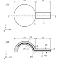
- FIG. 1 is a perspective view of a multilayer substrate 101 according to the first preferred embodiment.
- 2 is a plan view of the multilayer substrate 101, and the lower part of FIG. 2 is a cross-sectional view of the multilayer substrate 101 taken along a dashed line shown in the upper part of FIG.
- FIG. 3 is a cross-sectional view of a multilayer substrate 102 according to the second embodiment.
- FIG. 4 is a cross-sectional view of an electronic device 201 according to the third embodiment.
- FIG. 5 is a cross-sectional view of an electronic device 202 according to the fourth embodiment.
- FIG. 6 is a cross-sectional view of another electronic device 203 according to the fourth embodiment.
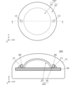
- FIG. 7 is a plan view of an electronic device 204 according to the fifth embodiment, and the lower part of FIG. 7 is a cross-sectional view of the electronic device 204 taken along the dashed line shown in the upper part.
- the upper part of Fig. 8 is a plan view of a multilayer substrate 107 according to a sixth embodiment, and the lower part of Fig. 8 is a cross-sectional view of an electronic device 205 including the multilayer substrate 107 shown in the upper part of Fig. 8 .
- FIG. 9 is a plan view of another multilayer substrate 108 according to the sixth embodiment.
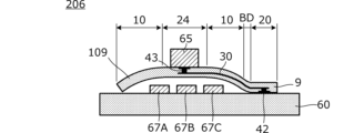
- FIG. 10 is a cross-sectional view of an electronic device 206 according to a seventh embodiment, which is configured by mounting a multilayer substrate 109 on which electronic components 65 are mounted on a circuit board 60.
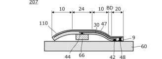
- FIG. 11 is a cross-sectional view of an electronic device 207 according to the seventh embodiment, which is configured by mounting a multilayer substrate 110 on which electronic components 66 are mounted, on a circuit board 60.
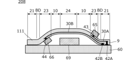
- FIG. 12 is a cross-sectional view of an electronic device 208 according to the seventh embodiment, which is configured by mounting a multilayer substrate 111 on which electronic components 65 and 66 are mounted, on a circuit board 60.
- 13 is a plan view of an electronic device 209 according to the eighth embodiment, and the lower part of FIG.
- FIG. 13 is a cross-sectional view of the electronic device 209 taken along the dashed line in the upper part of FIG. 14 is a plan view of another multilayer substrate 113 according to the eighth embodiment, and the lower part of FIG. 14 is a cross-sectional view of the multilayer substrate 113 taken along the dashed line in the upper part of FIG.
- An upper part of Fig. 15 is a plan view of an electronic device 210 according to a ninth embodiment, and a lower part of Fig. 15 is a cross-sectional view taken along a dashed line in the upper part of Fig. 15 .
- the upper part of Fig. 16 is a plan view of another electronic device 211 according to the ninth embodiment, and the lower part of Fig.
- FIG. 16 is a cross-sectional view taken along the dashed line in the upper part of Fig. 16 .
- the upper part of Fig. 17 is a plan view of a multilayer substrate 115 according to the tenth embodiment, and the lower part of Fig. 17 is a cross-sectional view taken along the dashed line in the upper part of Fig. 17.
- FIG. 18 is a perspective view of a multilayer substrate 116 according to the eleventh embodiment.
- the upper part of FIG. 19 is a plan view of electronic device 212 including multilayer substrate 116, and the lower part of FIG. 19 is a cross-sectional view taken along the dashed line shown in the upper part of FIG. FIG.
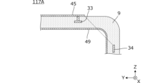
- FIG. 20 is a perspective view of a multilayer substrate 117A according to the twelfth preferred embodiment.
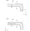
- the upper part of FIG. 21 is a cross-sectional view taken along the dashed line in FIG.
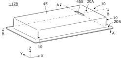
- FIG. 22 is a cross-sectional view of another multilayer substrate 117B according to the twelfth embodiment.
- FIG. 23 is a cross-sectional view taken along the dashed line in FIG.
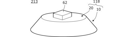
- FIG. 24 is a perspective view of an electronic device 213 including a multilayer substrate 118 according to the thirteenth embodiment and electronic components 62 mounted thereon.
- the upper part of Fig. 25 is a perspective view of an electronic device 214 including a multilayer substrate 119 according to the fourteenth embodiment and electronic components 62 mounted thereon.
- FIG. 25 is a cross-sectional view taken along the dashed line in the upper part of Fig. 25.
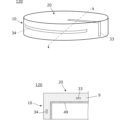
- FIG. 26 is a diagram showing another multilayer substrate 120 according to the fourteenth embodiment.
- the upper part of FIG. 27 is a perspective view of a multilayer substrate 121 according to the fifteenth embodiment, and the lower part of FIG. 27 is a vertical cross-sectional view taken at the position indicated by the dashed dotted line in the upper part of FIG. 28A to 28C are cross-sectional views of a multilayer substrate according to the sixteenth embodiment.
- 29A to 29C are cross-sectional views of a multilayer substrate according to the sixteenth embodiment.
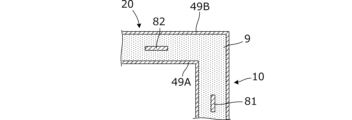
- Figure 30 is a cross-sectional view of a multilayer board according to the sixteenth embodiment, and is an example of a multilayer board having conductor patterns 81, 82 as signal lines and conductor patterns 49A, 49B as two ground conductor layers sandwiching them in the stacking direction.
- FIG. 31 is a cross-sectional view of a multilayer substrate according to a sixteenth embodiment, showing some examples of the positions at which conductor patterns serving as ground conductor layers are formed.
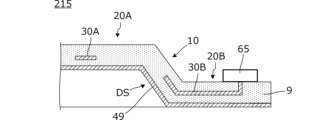
- FIG. 32 is a cross-sectional view of a main part of an electronic device 215 according to the seventeenth embodiment.
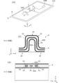
- the upper part of Figure 33 is an oblique view of electronic device 216 relating to the 18th embodiment
- the middle part of Figure 33 is a vertical cross-sectional view of multilayer substrate 122 at part X-X in the upper part of Figure 33
- the lower part of Figure 33 is a vertical cross-sectional view of multilayer substrate 122 at part Y-Y in the upper part of Figure 33
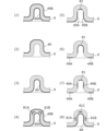
- FIG. 34 is a plan view of some other multilayer substrates according to the eighteenth embodiment.
- the upper and lower parts of FIG. 35 are cross-sectional views of another multilayer substrate according to the eighteenth embodiment.
- FIG. 36 is a cross-sectional view of some other multilayer substrates according to the eighteenth embodiment.
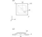
- FIG. 37 is a plan view of electronic device 217 including multilayer substrate 123 and electronic components 62 and 65, and the lower part of FIG. 37 is a vertical cross-sectional view taken along the dashed line in the upper part.
- the upper part of Fig. 38 is a partial cross-sectional view of electronic device 217.
- the lower part of Fig. 38 is a transverse cross-sectional view taken along the dashed line in the upper part of Fig. 38.
- FIG. 39 is a plan view of another electronic device according to the nineteenth embodiment.
- the upper part of FIG. 40 is a plan view of an electronic device 218 including a multilayer substrate 124 and an electronic component 62, and the lower part of FIG. 40 is a vertical cross-sectional view taken along the dashed line in the upper part.
- FIG. 41 is a partial cross-sectional view of electronic device 218.
- the middle part of Fig. 41 is a cross-sectional view taken along the dashed line at the upper part of the upper part of Fig. 41
- the lower part of Fig. 41 is a cross-sectional view taken along the dashed line at the lower part of the upper part of Fig. 41.
- FIG. 42 is a perspective view of electronic devices 219 and 220 according to the twenty-first embodiment.
- the upper part of FIG. 43 is a partial cross-sectional view of the first part 10 of the electronic device 219 shown in the upper part of FIG. 42, and the lower part of FIG.
- FIG. 43 is a partial cross-sectional view of the first part 10 of the electronic device 220 shown in the lower part of FIG. 42.
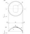
- FIG. 44 is an example of a plan view of a multi-layer board viewed from a protruding direction of the multi-layer board due to the presence of convex and concave curved surfaces of the multi-layer board.
- Fig. 1 is a perspective view of a multilayer substrate 101 according to the first embodiment.
- the upper part of Fig. 2 is a plan view of the multilayer substrate 101, and the lower part of Fig. 2 is a cross-sectional view of the multilayer substrate 101 shown in the upper part of Fig. 2 taken along a dashed line.
- the multilayer board 101 is a multilayer board formed by stacking multiple substrate layers 9.
- each substrate layer is integrated, so no lines are visible between adjacent substrate layers. Therefore, the substrate layer 9 in the figure is not a symbol that refers to a single substrate layer, but rather a single symbol that represents multiple substrate layers. This is the same for the other figures shown below.
- the multilayer substrate 101 includes a first portion 10 having a constant or approximately constant thickness between the opposing front and back surfaces, and a second portion 20 continuous with the first portion 10.
- the surface of the first portion 10 is at least one convex surface PS, and the back surface of the first portion 10 is a concave surface DS opposite the convex surface PS.
- the surface SS and back surface BS of the second portion 20 are flat surfaces.
- the convex surface PS is not a surface that curves around an axis perpendicular to the protruding direction.
- the Z-axis direction is the protruding direction.
- the convex surface PS is a spherical surface rather than a cylindrical surface.
- the cross section in a plane formed by two of the three orthogonal axes one of which is the protruding direction of the convex surface PS, describes a curve, and also describes a curve in a cross section in a plane formed by the other two axes.
- the concave surface DS faces the convex surface PS in order to maintain the thickness of the multilayer board.
- Each substrate layer 9 is continuous from the first portion 10 to the second portion 20.
- the conductor pattern 31 inside the first portion 10 and the conductor pattern 32 inside the second portion 20 are continuous.
- the angle between the first portion 10 and the second portion 20 varies depending on the position of the cross section, but for multiple cross sections passing through the boundary BD between the first portion 10 and the second portion 20, the minimum angle ⁇ between the first portion 10 and the second portion 20 at the boundary BD is an obtuse angle.
- the bent portion between the conductor patterns 31 and 32 may have a chamfered corner or a curved shape. This distributes the stress acting on the bent portion between the conductor patterns 31 and 32, so that damage to the bent portion between the conductor patterns 31 and 32 is more effectively suppressed.
- a conductor pattern 41 is formed on the surface of the first portion of the multilayer substrate 101.
- This conductor pattern 41 is, for example, a radiating element for an antenna, and is electrically connected to a conductor pattern 31 formed inside the multilayer substrate 101.
- the conductor pattern 41 and the conductor pattern 31 are connected by a connecting conductor that forms a conductive path in the stacking direction of the base layer 9.
- a stripline may be configured by forming ground conductor layers on the front and back surfaces of the multilayer substrate 101.
- the conductor pattern 41 and the conductor pattern 31 may be electromagnetically coupled or electric-field coupled.
- the outer shape of the first part 10 is circular when viewed from the protruding direction of the convex curved surface. Also, the outer shape of the second part 20 is rectangular when viewed from the protruding direction of the convex curved surface of the first part 10.
- the planar shape of the second portion 20 when viewed from the protruding direction of the convex curved surface (Z direction) is a shape that protrudes from a portion of the position surrounding the first portion 10.
- This second portion 20 may also be a shape that protrudes from the entire position surrounding the first portion 10.
- the material of the base layer 9 is, for example, a polyolefin resin such as styrene, polyethylene, or polypropylene, a thermoplastic resin such as a thermoplastic polyimide, or a fluororesin. This makes it easy to change the shape at the boundary BD between the first portion 10 and the second portion 20.
- the multilayer substrate 101 shown above is formed as a multilayer substrate having a first portion 10 and a second portion 20, for example, by stacking a plurality of base layers 9, including the base layer 9 on which the conductor patterns 31, 32 are formed, and simultaneously hot pressing the entire substrate using a mold having a convex curved surface and a mold having a concave curved surface.
- Second Embodiment In the second embodiment, an example in which the shape of the conductor pattern in the first portion and the structure of the second portion are different from those in the first embodiment will be described.
- FIG. 3 is a cross-sectional view of a multilayer substrate 102 according to the second embodiment.
- the plan view of this multilayer substrate 102 is similar to the multilayer substrate 101 shown in FIGS. 1 and 2.
- the multilayer substrate 102 includes a first portion 10 having a constant or approximately constant thickness between the opposing front and back surfaces, and a second portion 20 continuous with the first portion 10.
- the second portion 20 has a shape that is pulled outward from the first portion 10.
- the first portion 10 has a circuit portion that includes a substrate layer 9 and a conductor pattern.
- the first portion 10 has a second portion 21 that is pulled outward from the first portion 10. In this way, there may be multiple second portions. Also, the directions in which the second portions are pulled out from the first portion 10 may differ.
- the first portion 10 of the multilayer substrate 102 is provided with a connection conductor 51 that is electrically connected to the conductor pattern 31 formed inside the multilayer substrate 102 and forms a conductive path in the direction of stacking.
- a conductor pattern 41 is formed on the surface of the first portion 10.
- the connection conductor 51 provides electrical conductivity between the conductor pattern 31 and the conductor pattern 41.
- the second portion 20 has a transmission line including a substrate layer 9 and a conductor pattern 32. Near the end of the conductor pattern 32, there is a connection conductor 52 that is conductive to the conductor pattern 32 and forms a conductive path in the stacking direction.
- a connector 61 is mounted on the back surface of the second part 20, and the connection conductor 52 is connected to this connector 61.
- the conductor pattern 31 inside the first portion 10 and the conductor pattern 32 inside the second portion 20 are continuous.
- the second portion 20 partially has a thin region 22 of the second portion that is thinner than the first portion 10. This structure makes it easier to bend in the thin region 22 and reduces the stress applied to the conductor pattern 32 inside the thin region, preventing breakage of the conductor pattern 32.
- An example of a method for manufacturing the multilayer substrate 102 shown above is as follows.
- the first part 10 and the second part 20 of the multilayer substrate 102 are formed by hot pressing the base material layers 9 in a stacked state.
- FIG. 4 is a cross-sectional view of electronic device 201 according to the third embodiment.
- Electronic device 201 includes a circuit board 60, electronic components 62 mounted on circuit board 60, multi-layer board 103, and connector 61 attached to multi-layer board 103. Hatching indicating the cross-section has been omitted in FIG. 4 to prioritize clarity and visibility.
- a conductor pattern is formed in multi-layer board 103, but no conductor pattern is present at the cross-section position in FIG. 4.
- the outer shape (planar shape) of the multilayer substrate 103 when viewed from the protruding direction of the convex curved surface of the first portion 10 is circular.
- the planar shape of the second portion 20 before bending (or curving) when viewed from the protruding direction of the convex curved surface is a rectangle protruding from a portion of the position surrounding the first portion 10. By bending (curving) such a rectangular portion, bending (curving) of the second portion 20 becomes easier.
- This bent (curved) portion may be a portion corresponding to the thin region 22 in FIG. 3, i.e., a portion that is easier to bend (bend).
- the electronic components 62 are mounted on the portion of the circuit board 60 that is surrounded by the concave curved surface of the first portion 10 of the multilayer board 103.
- a predetermined conductor pattern is formed inside the multilayer board 103 and, if necessary, on the outer surface.
- the second portion 20 of the multilayer substrate 103 is bent (or curved) at two points so as to surround the end of the circuit board 60.
- the circuit of the circuit board 60 and the conductor pattern of the multilayer substrate 103 are electrically connected via a connector 61.
- the circuit board 60 or the electronic components 62 mounted thereon are connected to the conductor pattern formed in the second portion 20 of the multilayer substrate 103.
- the circuit board 60 is connected to the conductor patterns formed in the first portion 10 and the second portion 20 of the multilayer substrate 103.
- the first portion 10 of the multilayer substrate 103 by arranging the first portion 10 of the multilayer substrate 103 so as to cover the flat circuit board 60, a predetermined space can be formed between the first portion 10 of the multilayer substrate 103 and the circuit board 60.
- the second portion 20 of the multilayer substrate 103 by bending (or curving) the second portion 20 of the multilayer substrate 103, the second portion 20 can be made to reach the rear surface of the circuit board 60.
- the base layer 9 is made of a thermoplastic resin, the process freedom in manufacturing electronic devices is increased.
- an electronic device including a multilayer substrate having a hole formed in a first portion will be described as an example.
- FIG. 5 is a cross-sectional view of electronic device 202 according to the fourth embodiment.
- Electronic device 202 includes a circuit board 60, electronic components 62 mounted on circuit board 60, multi-layer board 104, and connector 61 attached to multi-layer board 104. Hatching indicating the cross-section has been omitted in FIG. 5 to prioritize clarity and visibility.
- a conductor pattern is formed in multi-layer board 104, but no conductor pattern is present at the cross-section position in FIG. 5.
- the external shape (planar shape) of the multilayer substrate 104 when viewed from the protruding direction of the convex curved surface of the first portion 10 is circular, and the planar shape of the second portion 20 before bending (or curving) is rectangular, protruding from a portion of the position surrounding the first portion 10.
- a specific circuit is configured on the circuit board 60.
- the electronic component 62 is, for example, a MEMS microphone.
- the circuit board 60 includes a circuit for the audio signal from this MEMS microphone.
- a predetermined conductor pattern is formed inside the multilayer substrate 104 and, if necessary, on its outer surface.
- a through hole H is formed in a part of the multilayer substrate 104.
- the through hole H is formed in a position close to the sound receiving part of the electronic component 62, which is a MEMS microphone.
- This through hole H has a sound collecting effect, so a microphone with a predetermined directivity can be formed.
- the electronic components 62 are arranged in a predetermined space between the first portion 10 of the multilayer substrate 104 and the circuit board 60, and a through hole H is provided in the multilayer substrate 104, which allows for an effective arrangement of the multilayer substrate 104 and the electronic components 62, making it easier to miniaturize the electronic device 202.
- FIG. 6 is a cross-sectional view of another electronic device 203 according to the fourth embodiment.
- This electronic device 203 includes a circuit board 60, a multilayer board 105, electronic components 62 mounted on this multilayer board 105, and a connector 61 attached to this multilayer board 105.
- FIG. 6 hatching indicating the cross-sectional portion has been omitted in order to prioritize clarity and visibility of the figure.
- a conductor pattern is formed in the multilayer board 105, but no conductor pattern is present at the cross-sectional position in FIG. 6.
- the outer and inner shapes of the multilayer substrate 105 when viewed from the protruding direction of the convex curved surface of the first portion 10 are both circular, and the second portion 24 is continuous with the inside of the inner shape.
- the planar shape of the second portion 20 before bending (or curving) is a rectangle that protrudes from a portion of the position surrounding the first portion 10.
- An electronic component 62 is mounted on the back surface of the second portion 24.
- the electronic component 62 is, for example, a MEMS microphone.
- a through hole H is formed in the second portion 24, and the electronic component 62 receives external sound through the through hole H.
- an electronic device including a multilayer substrate in which a cutout portion that constitutes a non-contact portion or non-pressing portion for an electronic component is formed in a first portion will be described as an example.
- FIG. 7 The upper part of FIG. 7 is a plan view of electronic device 204, and the lower part of FIG. 7 is a cross-sectional view of electronic device 204 taken along the dashed line shown in the upper part.
- This electronic device 204 includes a circuit board 60, a coaxial cable (electronic component) 70 connected to this circuit board 60 via a connector 63, a multi-layer board 106, and a connector 61 attached to this multi-layer board 106.
- FIG. 7 hatching indicating the cross-sectional portion has been omitted in order to prioritize clarity and visibility of the drawing.
- a conductor pattern 64 is formed in the circuit board 60.
- Conductor patterns 31 and 32 are formed inside the multilayer board 106 as radiating elements, for example.
- One end of the conductor pattern 64 is connected to the coaxial cable 70 via a connector 63, and the other end is connected to the conductor pattern 32 in the second part 20 of the multilayer board 106 via a connector 61.
- the first portion 10 of the multilayer substrate 106 is formed with a notched portion 10N that constitutes a non-contact portion for the coaxial cable 70, which is an electronic component.
- the multilayer substrate can be easily mounted together with the electronic components without contacting the electronic components (non-contact or non-pressing).
- a multilayer board in which a notch-shaped portion or an opening-shaped portion for fixing to a member having a predetermined shape is formed in the second portion, and an electronic device including the multilayer board will be illustrated.
- the upper part of FIG. 8 is a plan view of the multilayer substrate 107.
- the lower part of FIG. 8 is a cross-sectional view of an electronic device 205 including the multilayer substrate 107 shown in the upper part of FIG. 8. This cross-sectional view is taken at the position indicated by the dashed line shown in the upper part of FIG. 8.
- the multilayer substrate 107 is composed of a first portion 10 and a second portion 20.
- the first portion 10 has a shape equivalent to a part of a sphere or a part of a nearly spherical surface, and the second portion is a circular ring-shaped flat plate.
- the second portion is continuous around the first portion.
- An opening 13 is formed in the second portion 20 of the multilayer substrate 107.
- the electronic device 205 includes a circuit board 60, pins 68 provided on the circuit board 60, a multi-layer board 107, and a housing 71 that houses these.
- the multilayer board 107 is fixed by inserting its opening 13 into the pin 68 on the circuit board 60.
- FIG. 9 is a plan view of another multilayer substrate 108 according to the sixth embodiment.
- this multilayer substrate 108 is composed of a first portion 10 having a shape equivalent to a part of a sphere or a part of a nearly sphere, and a second portion 20 which is a circular ring-shaped flat plate.
- the multilayer substrate 108 has a cutout portion 12 formed in the second portion 20.
- the multilayer board 108 can be fixed by fixing the cutout portion to a member of a specified shape, such as part of a circuit board.
- the second part 20 is a circular ring shape, but the ring shape is not limited to a circle.
- the outer shape of the second part 20 may be a polygon such as a square, or a polygon with rounded corners.
- an electronic device including a multilayer substrate and electronic components mounted thereon will be described as an example.
- FIGS. 10, 11, and 12 are cross-sectional views of electronic devices according to the seventh embodiment.
- FIG. 10 is a cross-sectional view of electronic device 206 constructed by mounting multilayer substrate 109, on which electronic components 65 are mounted, on circuit substrate 60.
- Multilayer substrate 109 comprises first portion 10 and second portions 20, 24.
- First portion 10 has a planar shape that is a circular ring when viewed from the protruding direction of its convex curved surface.
- Second portion 24 has a circular shape when viewed from the protruding direction of the convex curved surface.
- Second portion 20 has an outer shape that is a rectangular parallelepiped when viewed from the protruding direction of the convex curved surface.
- the shape of the second part 24 when viewed from the protruding direction of the convex curved surface is not limited to a circle.
- it may be a polygon such as a square, or a polygon with rounded corners.
- the first part 10 when viewed from the protruding direction of the convex curved surface is not limited to a circular ring shape.
- it may be a polygonal ring such as a square, or a polygonal ring with rounded corners.
- the boundary BD between the second part 20 and the first part 10 is a concave surface on the front side of the multilayer substrate 109, and a convex surface on the back side opposite the concave surface.
- a conductor pattern 30 is formed on the inner layer of the multilayer substrate 109.
- a terminal electrode 42 is formed on the end of the multilayer substrate 109.
- a terminal electrode 43 for mounting an electronic component 65 is formed at a predetermined position on the surface of the multilayer substrate 109.
- the conductor pattern 30 acts as a wiring pattern between the terminal electrodes 42 and 43.
- Electronic components 67A, 67B, and 67C are mounted on the surface of the circuit board 60.
- the multilayer board 109 on which electronic components 65 are already mounted can be mounted on the circuit board 60.
- the electronic components 67A, 67B, and 67C are present in the space between the first part 10 and the second part 24 of the multilayer board 109 and the circuit board 60. Therefore, the electronic components 67A, 67B, and 67C can be protected by the multilayer board 109 against collisions with external objects.
- the electronic components 67A, 67B, and 67C can be arranged in the recessed parts of the multilayer board 109, the space in the recessed parts of the multilayer board 109 can be effectively utilized, and the overall size can be reduced.
- FIG. 11 is a cross-sectional view of electronic device 207 formed by mounting multilayer substrate 110, on which electronic components 66 are mounted, on circuit board 60.
- Multilayer substrate 110 has first portion 10, second portions 20 and 24, and boundary BD.
- the planar shape of multilayer substrate 110 is similar to the planar shape of multilayer substrate 109.
- Conductor patterns 30 and 47 are formed on the inner layers of the multilayer substrate 110. Terminal electrodes 42 and 48 are formed on the ends of the multilayer substrate 110. A terminal electrode 44 for mounting an electronic component 66 is also formed at a predetermined position on the rear surface of the multilayer substrate 110.
- the conductor pattern 30 acts as a wiring pattern between the terminal electrodes 42 and 44.
- the conductor pattern 47 forms a conductor layer that extends in the planar direction of the multilayer substrate 110. This conductor pattern 47 is connected to the ground of the circuit board 60 via the terminal electrode 48. Therefore, the entire lower part of the multilayer substrate 110, including the electronic component 66, is electromagnetically shielded. Note that the conductor pattern 47 does not need to be connected to the ground depending on the purpose of the electromagnetic shielding of the electronic component 66 or the lower part of the multilayer substrate 110.
- the conductor pattern 47 may also be formed on the upper surface of the multilayer substrate 110.
- the multilayer substrate 110 As shown in FIG. 11, by connecting the terminal electrodes 42 of the multilayer substrate 110 to the terminal electrodes of the circuit substrate 60, the multilayer substrate 110, on which electronic components 66 have already been mounted, can be mounted on the circuit substrate 60. In this manner, with the multilayer substrate 110 mounted on the circuit substrate 60, the electronic components 66 are present in the space between the first portion 10 and the second portion 24 of the multilayer substrate 110 and the circuit substrate 60. Therefore, the electronic components 66 can be protected by the multilayer substrate 110 against collisions with external objects, etc.
- FIG. 12 is a cross-sectional view of electronic device 208 constructed by mounting multilayer substrate 111 on which electronic components 65, 66 are mounted on circuit substrate 60.
- Multilayer substrate 111 includes first portion 10, second portions 21, 23, 24, and boundary BD.
- First portion 10 has a circular ring-shaped planar shape when viewed from the protruding direction of its convex curved surface.
- Second portion 24 has a circular shape when viewed from the protruding direction of the convex curved surface.
- Second portion 21 has a circular ring-shaped planar shape when viewed from the protruding direction of the convex curved surface.
- boundary BD between second portion 21 and second portion 23 also has a circular ring-shaped planar shape.
- Conductor patterns 30A and 30B are formed on the inner layers of multilayer substrate 111. Terminal electrodes 42A and 42B are formed on the ends of multilayer substrate 111. A terminal electrode 43 for mounting electronic component 65 is formed at a predetermined position on the front surface of multilayer substrate 111, and a terminal electrode 44 for mounting electronic component 66 is formed at a predetermined position on the back surface of multilayer substrate 111. Conductor pattern 30A acts as a wiring pattern between terminal electrode 42A and terminal electrode 43. Conductor pattern 30B acts as a wiring pattern between terminal electrode 42B and terminal electrode 44.
- electronic components may be mounted on both sides of a multi-layer board.
- FIG. 13 The upper part of FIG. 13 is a plan view of electronic device 209 according to the eighth embodiment, and the lower part of FIG. 13 is a cross-sectional view of electronic device 209 taken along the dashed line in the upper part of FIG. 13.
- Electronic device 209 is composed of multilayer substrate 112 and electronic components 69 mounted thereon.
- the multilayer substrate 112 includes a first portion 10 and second portions 21 and 24.
- a boundary BD is formed between the first portion 10 and the second portion 24.
- An electronic component 69 is mounted on the second portion 24 of the multilayer substrate 112.
- This multilayer board 112 has a horizontally cut doughnut-shaped space SP that is made up of curved surfaces including the first portion 10. In the cross section, as shown in FIG. 13, there are two spaces SP, SP. For example, electronic components or equipment members can be placed in these spaces.
- FIG. 14 The upper part of FIG. 14 is a plan view of another multilayer substrate 113 according to the eighth embodiment, and the lower part of FIG. 14 is a cross-sectional view of the multilayer substrate 113 taken along the dashed line in the upper part of FIG. 14.
- the multilayer substrate 113 includes first portions 10 and 11 and a second portion 21. A boundary is formed between the first portion 10 and the first portion 11. Also, a boundary is formed between the first portion 11 and the second portion 21.
- the multilayer substrate 113 has a horizontally cut doughnut-shaped space SP1 formed by a curved surface including the first portion 11.
- the multilayer substrate 113 also has a horizontally cut spherical space SP2 formed by a curved surface including the first portion 10.
- FIG. 15 The upper part of FIG. 15 is a plan view of electronic device 210 according to the ninth embodiment.
- the lower part of FIG. 15 is a cross-sectional view taken along the dashed line in the upper part of FIG. 15.
- This electronic device 210 includes a multilayer substrate 114 and a conductor pattern 45 formed on its surface.
- the multilayer substrate 114 is composed of a first portion 10 and a second portion 20.
- the outer shape of the planar shape of the first portion 10 is circular.
- the planar shape of the second portion 20 is a circular ring shape.
- a conductor pattern 30 is formed on the inner layer of the multilayer substrate 114.
- a terminal electrode 42 is formed on the end of the multilayer substrate 114.
- a conductor pattern 45 of the patch antenna is formed at a predetermined position on the surface of the multilayer substrate 114.
- One end of the conductor pattern 30 is connected to the terminal electrode 42 via a connection conductor that exists in the stacking direction of the base layer 9.
- the other end of the conductor pattern 30 is connected to a predetermined position of the conductor pattern 45 via a connection conductor that exists in the stacking direction of the base layer 9.
- a patch antenna may be formed in the first portion 10 of the multilayer substrate 114.
- FIG. 16 The upper part of FIG. 16 is a plan view of another electronic device 211 according to the ninth embodiment.
- the lower part of FIG. 16 is a cross-sectional view taken along the dashed line in the upper part of FIG. 16.
- This electronic device 210 includes a multilayer substrate 114 and a conductor pattern 46 formed on its surface.
- the multilayer substrate 114 is similar to the multilayer substrate 114 shown in FIG. 15.
- Conductor patterns 30A and 30B are formed on the inner layers of multi-layer substrate 114.
- Terminal electrodes 42A and 42B are formed on the ends of multi-layer substrate 114.
- a conductor pattern 46 of a double spiral antenna is formed at a predetermined position on the surface of the first portion 10 of the multilayer substrate 114.
- One end of the conductor patterns 30A and 30B is connected to terminal electrodes 42A and 42B, respectively, via a connection conductor that exists in the stacking direction of the base layer 9.
- the other end of the conductor patterns 30A and 30B is connected to the inner peripheral end of the conductor pattern 46 via a connection conductor that exists in the stacking direction of the base layer 9.
- a double spiral antenna may be formed in the first portion 10 of the multilayer substrate 114.
- a multilayer substrate in which the second portion is protruded by the first portion (that is, the protruding surface (protruding portion) includes a flat surface) will be described as an example.
- FIG. 17 The upper part of FIG. 17 is a plan view of a multilayer substrate 115 according to the tenth embodiment.
- the lower part of FIG. 17 is a cross-sectional view at the position indicated by the dashed line in the upper part of FIG. 17.
- This multilayer substrate 115 includes a first portion 10 and a second portion 20.
- the planar shape of the first portion 10 is a rectangular ring shape with rounded corners.
- the planar shape of the second portion 20 is a rectangle with rounded corners.
- the outer shape of the first portion 10 when viewed from the protruding direction of the convex curved surface is circular, but as in this embodiment, it may be polygonal. It may also be polygonal with rounded corners.
- the entire surface of the first part 10 is not a surface that curves around the axis in the protruding direction (Z direction), but rather the convex curved surface of the surface of the first part 10 exists at four points around the axis in the protruding direction (Z direction).
- FIG. 18 is a perspective view of a multilayer substrate 116 according to an eleventh embodiment.
- the upper part of FIG. 19 is a plan view of an electronic device 212 including the multilayer substrate 116, and the lower part of FIG. 19 is a cross-sectional view taken along the dashed line shown in the upper part of FIG. 19.
- This multilayer substrate 116 includes a first portion 10 and second portions 20A and 20B. As shown in Figures 18 and 19, the planar shape of the second portion 20A is a rectangle with rounded corners, and the planar shape of the second portion 20B is a rectangular ring shape with rounded inner corners.
- the front surface of the first portion 10 is a convex curved surface
- the back surface of the first portion 10 is a concave curved surface that faces the convex curved surface and provides thickness to the multilayer substrate 116
- the thickness between the opposing front and back surfaces of the second portions 20A and 20B is constant or approximately constant.
- a conductor pattern 45 serving as a radiating element (patch antenna) is formed on the inner layer of the substrate layer 9 of the second portion 20A.
- Conductor patterns 30A and 30B serving as wiring conductor patterns are formed on the inner layers of the substrate layer 9 of the second portions 20A and 20B and the first portion 10. One end of each of the conductor patterns 30A and 30B is connected to the conductor pattern 45 via an interlayer connection conductor.
- Terminal electrodes 42A, 42B, and 42C are formed on the second portion 20B, and these terminal electrodes 42A, 42, and 42C are exposed on the underside of the second portion 20B.
- the other ends of the conductor patterns 30A and 30B are continuous with the terminal electrodes 42A and 42B.
- These terminal electrodes 42A, 42B, and 42C act as mounting electrodes for the circuit board 60.
- Conductor patterns 64A and 64B as signal lines and a conductor pattern 64G as a ground conductor layer are formed on the circuit board 60.
- two points on the conductor pattern 45 serving as a radiating element are set as feeding points, so that the conductor pattern 45 can be used as a radiating element with two polarization planes.
- the multilayer substrate 116 may have two second portions 20A and 20B, and the second portion 20B mounted on the circuit board 60 may have terminal electrodes 42A, 42B, and 42C.
- the multilayer substrate 116 may have a circular or rectangular shape.
- the conductor pattern 45 as the radiating element may also have a circular or polygonal shape.
- the second portion 20B protruding from the first portion 10 does not have to be the entire area surrounding the first portion 10 (the entire circumference), but may be a portion protruding from a part of the first portion 10.
- the power supply point and the conductor pattern for power supply may be a single unit.
- the base layer 9 on which the conductor patterns 30A and 30B for power supply are formed may be thinner than the base layer 9 on which the conductor pattern 45 as the radiating element is formed.
- a cavity is provided between the power supply conductor patterns 30A, 30B and the conductor pattern 64G serving as the ground conductor layer. Since the cavity (air) has a lower dielectric constant than the base layer 9, the electromagnetic field coupling coefficient between the conductor patterns 30A and 30B can be reduced. This can improve the isolation of two signals with different polarization planes. Furthermore, this effect can be further enhanced by thinning the base layer 9 on which the power supply conductor patterns 30A, 30B are formed.
- the rigidity of the multilayer substrate 116 can be further increased by filling the cavity with a resin with a low dielectric constant.
- Twelfth embodiment an electronic device including a multilayer substrate on which an electromagnetic field shielding conductor pattern is formed will be exemplified.
- FIG. 20 is a perspective view of a multilayer substrate 117A according to the twelfth embodiment.
- FIG. 21 is a cross-sectional view taken along the dashed line in FIG. 20.
- the multilayer substrate 117A includes a first portion 10 and second portions 20A and 20B.
- the planar shape of the second portion 20A is a rectangle with rounded corners
- the planar shape of the second portion 20B is a rectangular ring shape with rounded corners on the inner circumference.
- the front surface of the first portion 10 is a convex curved surface
- the back surface of the first portion 10 is a concave curved surface facing the convex curved surface, which gives thickness to the multilayer substrate 117A.
- a conductor pattern 45 serving as a radiating element (patch antenna) is formed on the outer surface of the base layer 9 of the second portion 20A.
- Conductor patterns 33 and 34 serving as wiring conductor patterns are formed on the inner layer of the base layer 9 of the second portions 20A and 20B and the first portion 10. One end of the conductor pattern 33 is connected to the conductor pattern 45 via an interlayer connection conductor.
- a conductor pattern 49 is formed on the inner surface of the substrate layer 9.
- This conductor pattern 49 is formed as a ground conductor layer.
- the dashed lines indicate that the conductor pattern 49 exists between the conductor pattern 34 and the conductor pattern 45.
- the conductor pattern 49 suppresses interference between the radiating element and the signal line.
- a microstrip line is formed by the conductor pattern 49, the conductor pattern 33, and the substrate layer 9 that exists between them.
- a microstrip line is formed by the conductor pattern 49, the conductor pattern 34, and the substrate layer 9 that exists between them.
- a slot 45S is formed in the conductor pattern 45. That is, the slot antenna is formed by the conductor pattern 45 and the substrate layer 9.
- a conductor pattern 84 is formed on the inner layer of the substrate layer 9, and a strip line is formed by this conductor pattern 84, the conductor patterns 45 and 49 as the ground conductor layer, and the substrate layer 9. This strip line acts as a power supply line for the slot antenna.
- a portion of the laminated substrate can be used as a microstrip line or a strip line, eliminating the need to provide a separate signal transmission line and resulting in an integrated electronic device.
- FIG. 24 is a perspective view of an electronic device 213 that is configured with a multilayer substrate 118 according to the thirteenth embodiment and electronic components 62 mounted thereon.
- the multilayer substrate 118 is composed of a first portion 10 and a second portion 20.
- the first portion 10 and the second portion 20 are plate-shaped with a constant thickness.
- the front and back surfaces of the first portion 10 are not surfaces that curve around the axis in the protruding direction like a cylindrical surface, but are part of the side of a cone.
- the second portion 20 is in the shape of a circular or elliptical plate, and the surface is flat.
- the front and back surfaces of the first portion 10 of the multilayer substrate 118 are not limited to being part of a sphere or ellipsoid, and may be any curved surface.
- a conductor pattern formed in a first portion and a second portion of a multilayer substrate is different from the examples shown so far.
- the multilayer substrate according to the fourteenth embodiment is a multilayer substrate on which an electromagnetic field shielding conductor pattern is formed.
- FIG. 25 The upper part of FIG. 25 is a perspective view of an electronic device 214 that is composed of a multilayer substrate 119 according to the 14th embodiment and electronic components 62 mounted thereon.
- the multilayer substrate 119 is composed of a first portion 10 and a second portion 20.
- the first portion 10 and the second portion 20 are plate-shaped and have a constant thickness.
- the shapes of the first portion 10 and the second portion 20 are similar to the example shown in Figure 24.
- the electronic device 214 is mounted on a circuit board not shown.
- a conductor pattern 34 is formed on the inner layer of the first portion 10. Furthermore, a conductor pattern 33 is formed on the inner layers from the first portion 10 to the second portion 20.
- the conductor pattern 34 is a signal line for a transmission signal.
- the conductor pattern 33 is a signal line that is conductive at one end to a terminal electrode of the electronic component 62 and conductive at the other end to a terminal electrode of the circuit board.
- a conductor pattern 49 is formed as a ground conductor on or near the inner surface of the first portion 10 and the second portion 20.
- the conductor pattern 49 is present between the conductor pattern 33 and the conductor pattern 34.
- the conductor pattern 49 electromagnetically shields the conductor pattern 33 and the conductor pattern 34. In other words, it suppresses interference between the conductor pattern 33 and the conductor pattern 34.
- the conductor pattern 49, the conductor pattern 33, and the substrate layer 9 form a microstrip line.
- the conductor pattern 49, the conductor pattern 34, and the substrate layer 9 form a microstrip line.
- the conductor pattern 49, the conductor pattern 34, and the substrate layer 9 form a microstrip line.
- the conductor pattern 49, the conductor pattern 34, and the substrate layer 9 form a microstrip line.
- the front surface of the first portion 10 is a convex curved surface PS
- the back surface of the first portion 10 is a concave curved surface DS that faces the convex curved surface PS and adds thickness to the multilayer substrate 119.
- the internal space of this concave curved surface DS acts as an electromagnetic field shielding conductor for, for example, a circuit board or electronic components mounted on the circuit board.
- the conductor pattern 49 is not only the ground conductor layer of the microstrip line, but also electromagnetically shields the circuit board present inside the recess formed by the concave curved surface DS and the electronic components mounted on the circuit board.
- FIG. 26 shows another multilayer substrate 120 according to the 14th embodiment.
- FIG. 26 is an oblique view showing the internal structure of the first part 10, and the lower part of FIG. 26 is a cross-sectional view taken along the dashed line in the upper part of FIG. 26.
- a conductor pattern 34 is formed on the inner layer of the first portion 10.
- a conductor pattern 33 is formed on the inner layers from the first portion 10 to the second portion 20.
- the conductor pattern 34 is a signal line or a radiating element for a transmission signal.
- the present invention can be applied in the same way even if the first part is cylindrical.
- FIG. 27 The upper part of FIG. 27 is a perspective view of a multilayer substrate 121 according to the fifteenth embodiment, and the lower part of FIG. 27 is a vertical cross-sectional view taken at the position indicated by the dashed line in the upper part of FIG. 27.
- the multilayer substrate 121 includes a first portion 10 and second portions 20A and 20B.
- the planar shape of the second portion 20A is a rectangle with rounded corners
- the planar shape of the second portion 20B is a rectangular ring shape with rounded inner corners.
- the front surface of the first portion 10 is a convex curved surface
- the back surface of the first portion 10 is a concave curved surface facing the convex curved surface, which gives thickness to the multilayer substrate 121.
- Conductor patterns 81 and 82 are formed as wiring patterns inside the base layer 9 of the second portion 20A.
- a conductor pattern 49 is formed as a ground conductor on the inner surface or near the inner surface of the first portion 10 and the second portions 20A and 20B.
- the conductor pattern 49, the conductor patterns 81 and 82, and the base layer 9 each form a microstrip line.
- sixteenth embodiment In the sixteenth embodiment, various arrangement examples of conductor patterns as signal lines and conductor patterns as ground conductor layers formed in the first and second portions of a multilayer substrate will be illustrated.
- FIGS 28 to 31 are cross-sectional views of each multilayer board according to the 16th embodiment.
- the three cross-sectional views shown in FIG. 28 are cross-sectional views taken at positions passing through the first portion 10 and the second portion 20A of the multilayer substrate.
- the two-dot chain line represents the boundary surface between the first portion 10 and the second portion 20A.
- a conductor pattern 82 serving as a signal line is formed in the second portion 20A, and a conductor pattern 81 serving as a signal line is formed in the first portion 10.
- the conductor pattern 49 suppresses interference between the conductor patterns 81 and 82.
- the conductor pattern 82 serving as a signal line may be formed in the second portion 20A, which is the top surface.
- a conductor pattern 83 serving as a ground conductor is formed between conductor patterns 81 and 82 serving as signal lines, in the same layer as conductor patterns 81 and 82.
- conductor pattern 83 acts as a ground conductor layer.
- conductor pattern 83 increases the structural strength of the bent portion, loss of conductor pattern 49 is suppressed.
- conductor pattern 49 formed on the inner layer of substrate layer 9 suppresses interference between conductor pattern 81 and conductor pattern 82.
- a conductor pattern 83 serving as a ground conductor is formed between conductor patterns 81 and 82 serving as signal lines, and an interlayer connection conductor 53 is formed to provide electrical continuity between the conductor pattern 83 serving as a ground conductor and the conductor pattern 49 serving as a ground conductor.
- the conductor pattern serving as a ground conductor inside the base layer 9 may be electrically connected to the ground conductor layer extending on or near the surface of the base layer 9.
- the first portion 10 is a cylindrical portion
- the second portion 20 is a planar portion.
- conductor patterns 81A and 81B as signal lines are formed in the first portion 10 at positions that sandwich the conductor pattern 49 as the ground conductor layer.
- the conductor patterns 81A and 81B as signal lines may be formed at positions that correspond to different side surfaces in the cross-sectional view.
- the conductor pattern 49 suppresses interference between the conductor patterns 81A and 81B.
- Conductor patterns 81, 82 are formed as signal lines on each of the base layers 9, but they are formed on different layers. In this way, the conductor patterns 81, 82 may be formed on different layers of the base layer 9.
- the dashed double-dashed lines indicate the boundary surfaces between the first portion 10 and the second portions 20A and 20C.
- a conductor pattern 83 serving as a signal line is formed in the first portion 10
- a conductor pattern 81 serving as a signal line is formed in the second portion 20C.
- Figure 30 shows an example of a multilayer board having conductor patterns 81, 82 as signal lines and conductor patterns 49A, 49B as two ground conductor layers sandwiching them in the stacking direction.
- conductor pattern 81 as a signal line is formed inside substrate layer 9 of first portion 10
- conductor pattern 82 as a signal line is formed inside substrate layer 9 of second portion 20.
- Conductor pattern 49A as a ground conductor layer is formed on the inner surface of substrate layer 9, and conductor pattern 49B as a ground conductor layer is formed on the outer surface.
- Conductor patterns 81, 82 are disposed between conductor patterns 49A, 49B.
- conductor pattern 49B as a ground conductor layer, conductor patterns 81 and 82 as signal lines are electromagnetically shielded from external noise. In addition, radiation of noise from conductor patterns 81 and 82 to the outside is suppressed. Conductor pattern 49A also suppresses interference between conductor patterns 81 and 82.
- These conductor patterns 49A and 49B, the conductor patterns 81 and 82, and the base layer 9 each form a stripline.
- Figure 31 shows some examples of the positions where conductor patterns are formed as ground conductor layers.
- the conductor pattern 49A serving as the inner ground conductor layer is formed inside the base layer 9 near the inner surface, rather than on the inner surface of the base layer 9.
- the conductor pattern 49B serving as the outer ground conductor layer is formed inside the base layer 9 near the outer surface, rather than on the outer surface of the base layer 9.
- conductor pattern 49A as the inner ground conductor layer is formed inside substrate layer 9 near the inner surface of substrate layer 9.
- Conductor pattern 49B as the outer ground conductor layer is formed inside substrate layer 9 near the outer surface of substrate layer 9.
- the conductor pattern 49A, the conductor pattern 49B, or both are provided inside (inner layer) of the base layer 9, but the exposed surfaces of the conductor patterns 49A and 49B may be covered with a resist film to make the conductor pattern 49A, 49B, or both, non-exposed.
- FIG. 32 is a cross-sectional view of the main part of an electronic device 215 shown in the seventeenth embodiment.
- Conductor patterns 30A and 30B are formed as signal lines inside the base layer 9, and a conductor pattern 49 is formed as a ground conductor layer on the inner surface of the base layer 9.
- An electronic component 65 is mounted on the top surface of the second portion 20B.
- conductor pattern 49 electromagnetically shields the circuit board present inside the recess formed by concave surface DS and the electronic components mounted on the circuit board.
- Eighteenth embodiment In the eighteenth embodiment, a multilayer board having ribs and an electronic device including the same will be described as an example.
- the upper part of FIG. 33 is a perspective view of electronic device 216 according to the 18th embodiment
- the middle part of FIG. 33 is a vertical cross-sectional view of multilayer substrate 122 at part X-X in the upper part of FIG. 33
- the lower part of FIG. 33 is a vertical cross-sectional view of multilayer substrate 122 at part Y-Y in the upper part of FIG. 33.
- electronic device 216 includes multilayer substrate 122 and electronic components 69A, 69B mounted on multilayer substrate 122.
- Multilayer substrate 122 includes base layer 9 and a conductor pattern.
- part of the second part 20 of the multilayer board 122 forms a flat surface that extends in a plane, and the first part 10 forms a rib 8 that protrudes from the flat surface.
- the ribs 8 are formed as part of the multilayer substrate 122 by drawing the base layer 9 made of thermoplastic resin.
- the rib 8 When viewed in the stacking direction (Z direction) of the base material layer 9 of the second portion 20, the rib 8 forms a closed loop surrounding the flat portion.
- two rectangular closed loops are adjacent to each other.
- the multilayer board 122 includes a conductor pattern 81 as a signal line, and two conductor patterns 49A, 49B as ground conductor layers sandwiching it in the stacking direction.
- the conductor pattern 81 as a signal line is patterned in a direction perpendicular to the extension direction of the rib 8.
- a conductor pattern 83 as a ground conductor layer is formed in the same layer as the conductor pattern 81 as the signal line.
- the conductor patterns 49A, 49B are connected to this conductor pattern 83 via the interlayer connection conductor 53.
- the triplate stripline is composed of conductor pattern 81 as a signal line, conductor patterns 49A and 49B as two ground conductor layers sandwiching it in the stacking direction, and substrate layer 9 between conductor patterns 49A and 49B and conductor pattern 81.
- the rigidity of the multilayer board 122 is increased by the protrusion of the closed loop rib 8, and the planar shape stability of the multilayer board 122 and the electronic device 216 is high.
- the rib 8 also has a conductor pattern 81 as a signal line, conductor patterns 49A and 49B as ground conductor layers, a conductor pattern 83, and an interlayer connection conductor 53, so that the rigidity improvement effect of the rib 8 is high.
- FIG. 34 is a plan view of several other multilayer boards according to the eighteenth embodiment.
- the rib 8 may have a single closed loop.
- the rib 8 may have three or more closed loops.
- the rib 8 may not only form a closed loop, but also have a portion that extends inward of the closed loop.
- the rib 8 may be composed of a rib that forms a closed loop and another rib that is independent of the rib.
- the extension directions of the ribs 8 are not limited to being perpendicular to each other, and as shown in (6), (7), and (8), the ribs may include ribs extending in non-perpendicular directions.
- FIG. 35 The upper and lower parts of FIG. 35 are cross-sectional views of another multilayer board according to the 18th embodiment.
- the cross-sectional positions of these cross-sectional parts correspond to the cross-sectional positions of the cross-sectional views shown in the middle and lower parts of FIG. 33.
- the example shown in FIG. 35 includes a conductor pattern 81 as a signal line and a conductor pattern 49 as one ground conductor layer.
- a microstrip line is formed by the conductor pattern 81 as the signal line, the conductor pattern 49 as the ground conductor layer, and the substrate layer 9 between the conductor pattern 49 and the conductor pattern 81.
- the transmission line perpendicular to the extension direction of the rib 8 may be a microstrip line.
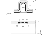
- FIG. 36 shows cross-sectional views of several other multilayer boards according to the 18th embodiment.
- the cross-sectional positions of these cross-sectional views correspond to the cross-sectional positions of the cross-sectional view shown in the center of FIG. 33.
- the rib does not necessarily have to have a conductor pattern formed as a signal line.
- the conductor pattern may be formed only on the outer surface of the rib.
- the conductor pattern may be formed only on the inner surface of the rib.
- the conductor patterns 81A and 81B as signal lines may extend in the extension direction of the rib.
- the conductor patterns 49A and 49B as ground conductor layers may be formed on the lower surface of the base layer 9, and the conductor pattern 81 as a signal line extending in the extension direction of the rib may be formed.
- This structure may be used as a coplanar waveguide.
- the conductor patterns 49A and 49B as ground conductor layers may be formed on the inner surface of the rib, and the conductor patterns 49A and 49B as external electrodes may be formed on the lower surface of the second portion.
- conductor patterns 81A, 81B, and 81C may be formed as signal lines on the inner layer of the rib, and a conductor pattern 49 may be formed as a ground conductor layer on the lower surface of the base layer 9.
- three microstrip lines may be formed, each extending in the extension direction of the rib.
- both ends of the signal line are pulled out to the outer layer by the interlayer connection conductor, making it easy to connect to connectors, chip components, ICs, etc. It is also easy to connect to other transmission lines by soldering, etc.
- FIG. 37 The upper part of FIG. 37 is a plan view of electronic device 217 including multilayer substrate 123 and electronic components 62, 65, and the lower part of FIG. 37 is a vertical cross-sectional view taken along the dashed line in the upper part.
- the upper part of Figure 38 is a partial cross-sectional view of electronic device 217. Here, hatching of base layer 9 has been omitted to clarify the figure.
- the lower part of Figure 38 is a cross-sectional view taken along the dashed dotted line in the upper part of Figure 38. Again, hatching of base layer 9 has been omitted to clarify the figure.
- the substrate layer 9 is formed with two microstrip lines MSL by the conductor pattern 49 as a ground conductor layer, the conductor pattern 81 as a signal line, and mainly the substrate layer 9 between them.
- a conductor pattern 80 is formed to face the portion of the conductor pattern 81 that expands in the layer direction.
- a plurality of interlayer connection conductors 53 are formed at positions arranged with a predetermined width in the layer direction, which conduct the conductor patterns 80 and 81 to each other in the stacking direction of the substrate layer 9.
- a waveguide is formed by the conductor patterns 80 and 81, the plurality of interlayer connection conductors 53, and the substrate layer 9 between the conductor patterns 80 and 81 and the plurality of interlayer connection conductors 53. Since the interval between the conductor patterns 81 and 82 is sufficiently thinner than a half wavelength, the TE10 mode is used as the propagation mode. If the interval between the interlayer connection conductors 53 is sufficiently narrower than one wavelength (approximately 1/10 wavelength or less), electromagnetic waves in the TE mode can propagate without being radiated outward.
- This waveguide can be called a substrate integrated waveguide (SIW).
- the propagating signal propagates through the microstrip line MSL as a TEM mode electromagnetic wave and through the waveguide SIW as a TE mode electromagnetic wave.
- the electronic component 65 shown in the upper part of Figure 38 is a chip antenna. Also, the electronic component 62 is a communication IC (semiconductor element for antenna) that uses the antenna to transmit and/or receive communication signals.
- IC semiconductor element for antenna
- the conductor pattern 81 within the range of the microstrip line MSL is tapered to improve the matching between the characteristic impedance of the microstrip line MSL and the characteristic impedance of the waveguide.
- the waveguide SIW connecting the antenna and IC can be bent in a three-dimensional curved shape of the multilayer substrate 123. This improves the freedom of layout and wiring design of each part.
- FIG. 39 is a plan view of another electronic device according to the nineteenth embodiment.
- eight electronic components 65 serving as chip antennas are mounted on the protruding portion of the multi-layer substrate.
- six electronic components 65 serving as chip antennas are mounted on the protruding portion of the multi-layer substrate. In this manner, multiple chip antennas each facing in a different direction may be arranged.
- the example shown in the lower part of Figure 39 shows an IC 62 mounted on the second part of the multilayer board. It is preferable to arrange the electronic component 65 and IC 62 (antenna semiconductor element) as each chip antenna, as shown in the already-mentioned microstrip line MSL and waveguide SIW, so that the signal propagates along the route with the shortest distance, and this is possible in this embodiment.
- a conductor pattern as a patch antenna may be formed on the multilayer board.
- FIG. 40 The upper part of FIG. 40 is a plan view of an electronic device 218 including a multilayer substrate 124 and electronic components 62, and the lower part of FIG. 40 is a vertical cross-sectional view taken along the dashed line in the upper part.
- the upper part of Figure 41 is a partial cross-sectional view of electronic device 218.
- hatching of base layer 9 has been omitted to clarify the drawing.
- the middle part of Figure 41 is a cross-sectional view taken along the dashed dotted line at the upper part of the upper part of Figure 41
- the lower part of Figure 41 is a cross-sectional view taken along the dashed dotted line at the lower part of the upper part of Figure 41.
- hatching of base layer 9 has been omitted to clarify the drawing.
- the microstrip line MSL is formed on the substrate layer 9 by the conductor pattern 49 as a ground conductor layer, the conductor pattern 81 as a signal line, and mainly the substrate layer 9 between them.
- a conductor pattern 80 is formed to face the portion of the conductor pattern 81 that expands in the layer direction.
- a plurality of interlayer connection conductors 53 are formed at positions arranged with a predetermined width in the layer direction, which conduct the conductor patterns 80 and 81 to each other in the stacking direction of the substrate layer 9.
- the conductor patterns 80 and 81, the plurality of interlayer connection conductors 53, and the substrate layer 9 between the conductor patterns 80 and 81 and the plurality of interlayer connection conductors 53 form a waveguide SIW.
- An opening AP is formed in the conductor pattern 80 above the waveguide SIW.
- a conductor pattern 84 is formed above the conductor pattern 80, and the conductor pattern 80 and the conductor pattern 84 are conductive via the interlayer connection conductor.
- Electronic device 218 has a metal housing 72.
- An opening 72S is formed in this housing 72. This opening 72S acts as a radiator for the slot antenna.
- an opening 72S is provided in the housing 72 to function as a slot antenna, but this can be applied to cases where there is a cover member, not limited to the housing.
- a metal cover is placed on the top surface of the multilayer board 124, a slot can be formed in the metal cover.
- FIG. 42 is a perspective view of electronic devices 219, 220 according to the 21st embodiment.
- the electronic device 219 shown in the upper part of FIG. 42 is composed of a multilayer board and multiple electronic components 65.
- the multilayer board has a first portion 10 and a second portion 20 that is continuous with the first portion 10.
- the first portion 10 has a spherical crown shape.
- the electronic components 65 are antenna elements and are arranged around the periphery of the spherical crown shape. These multiple antenna elements form an array antenna.
- the electronic device 220 shown in the lower part of Figure 42 is composed of a multilayer board and multiple electronic components 65.
- the multilayer board has a first portion 10 and a second portion 20 that is continuous with the first portion 10.
- the first portion 10 and the second portion 20 form a truncated cone shape.
- Each of the electronic components 65 is an antenna element, and is arranged around the periphery of the cone shape. These multiple antenna elements form an array antenna.
- an array antenna with isotropic directivity can be easily constructed.
- the curvature of the location where each antenna element is arranged is constant, the stress applied to the interlayer connection conductor formed in first portion 10 is uniform, resulting in high reliability.
- the upper part of FIG. 43 is a partial cross-sectional view of the first part 10 of the electronic device 219 shown in the upper part of FIG. 42
- the lower part of FIG. 43 is a partial cross-sectional view of the first part 10 of the electronic device 220 shown in the lower part of FIG. 42.
- a via hole facing in an oblique direction is formed in the first part 10, and the via hole is filled with a conductor to provide the interlayer connection conductor.
- the stress acting on the interlayer connection conductor is normal to the inner and outer surfaces of the first part 10, as shown by the dashed line, so that the allowable stress of the interlayer connection conductor is large. In other words, the interlayer connection conductor has high reliability against stress.
- the thickness of the first and second parts of the multilayer substrate is constant, but the thickness of either the first or second part may differ depending on the region. Also, the thickness of the first and second parts may differ.
- Figures 1, 7, 15, and 16 show examples in which circuit elements such as antenna elements and coil elements are formed in the first part of the multilayer substrate, but circuit elements using conductor patterns may also be configured in the second part of the multilayer substrate.
- the conductor pattern formed on the first portion 10 is connected to a circuit board or electronic components through the conductor pattern formed on the second portion 20, but the conductor pattern formed on the first portion 10 may be directly connected to the circuit board or electronic components.
- the planar shape of the multilayer board when viewed from the protruding direction of the multilayer board due to the presence of the convex curved surface PS and the concave curved surface DS of the multilayer board is approximately circular or approximately rectangular, but it may also be hexagonal, triangular, polygonal with a partial recess, or partially rounded, for example, as shown in FIG. 44. This also makes it possible to increase the degree of freedom in mounting on a circuit board or in assembling within a housing.
- a microstrip line is used as part of the power supply transmission path, but a triplate strip line may be configured as the power supply transmission path.
Landscapes
- Engineering & Computer Science (AREA)
- Microelectronics & Electronic Packaging (AREA)
- Manufacturing & Machinery (AREA)
- Structure Of Printed Boards (AREA)
Abstract
複数の基材層及び導体パターンを含み、これら基材層が積層されて成る多層基板(101)であり、それぞれ、互いに対向する表裏面間の厚みが一定又は略一定である第1部分(10)及び当該第1部分(10)に連続する第2部分(20)を備える。第1部分(10)の表面は少なくとも1つの凸曲面であり、第1部分(10)の裏面は凸曲面に対向する凹曲面であり、第2部分(20)の表裏面は平面であり、各基材層は第1部分(10)から第2部分(20)にかけて連続し、導体パターンの少なくとも一部は、多層基板(101)の内部において、第1部分(10)から第2部分(20)にかけて連続している。
Description
本発明は、複数の基材層が積層されて成る多層基板、この多層基板の製造方法、及びその多層基板を備える電子機器に関する。
特許文献1には、熱可塑性液晶ポリマーの特性を活かした、段差を有する電子デバイスの支持体が示されている。例えば、フィルムで構成される、又はその積層構造体で構成される支持体が、絞り加工によって勾配を有する段差が形成された電子デバイスが示されている。
特許文献1に記載の電子デバイスの支持体は立体的な熱可塑性液晶ポリマーで構成されているが、この支持体は、その表層にのみ導体パターンが形成されている構造体である。そのため、支持体に設ける配線の自由度が低い。
そこで、本発明の目的は、導体パターン形成上の自由度の高い多層基板、この多層基板の製造方法、及びその多層基板を備える電子機器を提供することにある。
(1)本開示の一例としての多層基板は、
複数の基材層及び導体パターンを含み、前記基材層が積層されて成る多層基板であり、
それぞれ、互いに対向する表裏面間の厚みが一定又は略一定である、第1部分及び当該第1部分に連続する第2部分を備え、
前記第1部分の表面は凸曲面であり、前記第1部分の裏面は前記凸曲面に対向して前記多層基板に前記厚みをもたせる凹曲面であり、
前記第2部分の前記表裏面は平面であり、
各前記基材層は前記第1部分から前記第2部分にかけて連続していて、
前記導体パターンの少なくとも一部は、前記多層基板の内部において、前記第1部分から前記第2部分にかけて連続している、ことを特徴とする。
複数の基材層及び導体パターンを含み、前記基材層が積層されて成る多層基板であり、
それぞれ、互いに対向する表裏面間の厚みが一定又は略一定である、第1部分及び当該第1部分に連続する第2部分を備え、
前記第1部分の表面は凸曲面であり、前記第1部分の裏面は前記凸曲面に対向して前記多層基板に前記厚みをもたせる凹曲面であり、
前記第2部分の前記表裏面は平面であり、
各前記基材層は前記第1部分から前記第2部分にかけて連続していて、
前記導体パターンの少なくとも一部は、前記多層基板の内部において、前記第1部分から前記第2部分にかけて連続している、ことを特徴とする。
(2)本開示の一例としての多層基板の製造方法は、
前記第1部分に、前記多層基板の内部に形成された前記導体パターンに導通し、前記積層の方向に導通路を形成する接続導体を備える、多層基板の製造方法であり、
前記多層基板の前記第1部分及び前記第2部分は、前記基材層を積層した状態で加熱プレスすることにより形成し、
前記積層の方向の開口部に導電性ペーストを入れ、加熱プレスすることにより、前記導電性ペーストを前記導通路として形成する、ことを特徴とする。
前記第1部分に、前記多層基板の内部に形成された前記導体パターンに導通し、前記積層の方向に導通路を形成する接続導体を備える、多層基板の製造方法であり、
前記多層基板の前記第1部分及び前記第2部分は、前記基材層を積層した状態で加熱プレスすることにより形成し、
前記積層の方向の開口部に導電性ペーストを入れ、加熱プレスすることにより、前記導電性ペーストを前記導通路として形成する、ことを特徴とする。
(3)本開示の一例としての電子機器は、
前記多層基板と、電子部品とを含む電子機器であり、
前記電子部品は前記第1部分の内部又は前記第2部分に配置されている、ことを特徴とする。
前記多層基板と、電子部品とを含む電子機器であり、
前記電子部品は前記第1部分の内部又は前記第2部分に配置されている、ことを特徴とする。
本発明によれば、導体パターン形成上の自由度の高い多層基板、この多層基板の製造方法、及びその多層基板を備える電子機器が得られる。
以降、図を参照して幾つかの具体的な例を挙げて、本発明を実施するための複数の形態を示す。各図中には同一箇所に同一符号を付している。要点の説明又は理解の容易性を考慮して、実施形態を説明の便宜上、複数の実施形態に分けて示すが、異なる実施形態で示した構成の部分的な置換又は組み合わせは可能である。第2の実施形態以降では第1の実施形態と共通の事柄についての記述を省略し、異なる点についてのみ説明する。特に、同様の構成による同様の作用効果については実施形態毎には逐次言及しない。
《第1の実施形態》
第1の実施形態では多層基板の一例について示す。図1は第1の実施形態に係る多層基板101の斜視図である。図2の上部は多層基板101の平面図であり、図2の下部は、図2の上部に示す多層基板101の一点鎖線での断面図である。
第1の実施形態では多層基板の一例について示す。図1は第1の実施形態に係る多層基板101の斜視図である。図2の上部は多層基板101の平面図であり、図2の下部は、図2の上部に示す多層基板101の一点鎖線での断面図である。
多層基板101は複数の基材層9が積層されて成る多層基板である。図2の下部に示す断面図では、各基材層は一体化されているので、隣接する基材層間の線は表れていない。したがって、図中の基材層9は、単一の基材層を指す符号ではなく、複数の基材層を単一の符号で表したものである。このことは、以降に示す他の図についても同様である。
多層基板101は、それぞれ、互いに対向する表裏面間の厚みが一定又は略一定である第1部分10及び当該第1部分10に連続する第2部分20を備える。
第1部分10の表面は少なくとも1つの凸曲面PSであり、第1部分10の裏面は凸曲面PSに対向する凹曲面DSである。第2部分20の表面SS及び裏面BSは平面である。
凸曲面PSは、突出方向に対して直交する軸回りに湾曲する面ではない。図1、図2に示した例ではZ軸方向が突出方向である。この突出方向に対して直交する、例えばY軸回りに湾曲する面は円筒面である。図1、図2に示す例では、凸曲面PSは円筒面ではなく球面である。
凸曲面PSの形状を別に表現すれば、凸曲面PSの突出方向を一つの軸とする直交3軸のうち、2つの軸で構成される平面での断面で曲線を描き、且つ他の2つの軸で構成される平面での断面でも曲線を描く、と言える。図1、図2において、X,Y,Zの3軸の向きを上記直交3軸とすれば、凸曲面PSのX-Y平面での断面は円であり、凸曲面PSのY-Z平面での断面は円弧であり、凸曲面PSのX-Z平面での断面は円弧である。つまり、どの2軸平面でも断面は直線を描かない。
凹曲面DSは、多層基板の厚みを保つ関係で凸曲面PSに対向する。
各基材層9は第1部分10から第2部分20にかけて連続している。また、第1部分10の内部の導体パターン31と、第2部分20の内部の導体パターン32とは連続している。
図2において、第1部分10と第2部分20との境界BDを通る断面について、第1部分10と第2部分20との成す角度は断面の位置に応じて異なるが、第1部分10と第2部分20との境界BDを通る複数の断面について、境界BDにおいて第1部分10と第2部分20との成す最小角度θは鈍角である。この構造により、第1部分10と第2部分20との境界BDが曲げられても、導体パターン31,32の、特に境界BDにおける破損が抑制される。
なお、導体パターン31と導体パターン32との曲げ部(第1部分10と第2部分20との境界BD)は、角部が面取りされた形状や湾曲形状であってもよい。そのことにより、導体パターン31と導体パターン32との曲げ部に掛かる応力が分散されるので、この導体パターン31と導体パターン32との曲げ部の破損がより効果的に抑制される。
図1に示す例では、多層基板101の第1部分の表面に導体パターン41が形成されている。この導体パターン41は例えばアンテナ用放射素子であり、多層基板101の内部に形成されている導体パターン31に導通している。図2では表れていないが、基材層9の積層の方向に導通路を形成する接続導体で、導体パターン41と導体パターン31とは接続されている。
図2では、多層基板101の内部に導体パターン31,32を備えた例を示したが、導体パターン31,32のうち、伝送線路として用いる箇所には、多層基板101の表裏面にグランド導体層を形成することにより、ストリップラインを構成してもよい。
なお、導体パターン41と導体パターン31とを電磁界結合又は電界結合させてもよい。
第1部分10の凸曲面の突出方向から視た外形は円形状である。また、第1部分10の凸曲面の突出方向から視た第2部分20の外形は矩形状である。
また、図1、図2に示した例では、凸曲面の突出方向(Z方向)から視た第2部分20の平面形状は、第1部分10を取り囲む位置の一部から突出する形状である。この第2部分20は、第1部分10を取り囲む位置の全部から突出する形状であってもよい。
前記基材層9の素材は、例えば、スチレン、ポリエチレン、ポリプロピレン等のポリオレフィン系樹脂、熱可塑性ポリイミド、フッ素系樹脂等の熱可塑性樹脂である。このことにより、第1部分10と第2部分20との境界BDでの形状を変化させやすい。
以上に示した多層基板101は、例えば、導体パターン31,32を形成した基材層9を含む複数の基材層9を積層した状態で、それら全体を、凸曲面を有する金型及び凹曲面を有する金型により同時に加熱プレスすることにより、第1部分10及び第2部分20を有する多層基板として形成する。
《第2の実施形態》
第2の実施形態では、第1の実施形態に比べて、第1部分の導体パターンの形状及び第2部分の構造が異なる例について示す。
第2の実施形態では、第1の実施形態に比べて、第1部分の導体パターンの形状及び第2部分の構造が異なる例について示す。
図3は第2の実施形態に係る多層基板102の断面図である。この多層基板102の平面図は図1、図2に示した多層基板101と類似している。
多層基板102は、それぞれ、互いに対向する表裏面間の厚みが一定又は略一定である第1部分10及び当該第1部分10に連続する第2部分20を備える。
第2部分20の形状は前記第1部分10から外方へ引き出された形状である。第1部分10は、基材層9及び導体パターンを含んで構成された回路部を備える。また、図3に示した例では、第1部分10から外方へ引き出された第2部分21を備える。このように、第2部分は複数あってもよい。また、第1部分10から引き出す第2部分の引き出し方向は異なっていてもよい。
多層基板102の第1部分10には、多層基板102の内部に形成された導体パターン31に導通し、積層の方向に導通路を形成する接続導体51を備える。第1部分10の表面には導体パターン41が形成されている。接続導体51は導体パターン31と導体パターン41とを導通させる。
第2部分20は、基材層9及び導体パターン32を含んで構成された伝送線路を備える。導体パターン32の端部付近には、この導体パターン32に導通し、積層の方向に導通路を形成する接続導体52を備える。
第2部分20の裏面にはコネクタ61が搭載されていて、このコネクタ61に接続導体52が接続されている。
第1部分10の内部の導体パターン31と、第2部分20の内部の導体パターン32とは連続している。
第2部分20は第1部分10より厚みの薄い第2部分の薄部領域22を部分的に有する。この構造により、薄部領域22での屈曲が容易となり、かつ薄部領域内部の導体パターン32に加わる応力を抑えることができるので、導体パターン32の破断が防止できる。
以上に示した多層基板102の製造方法の例は次のとおりである。
先ず、多層基板102の第1部分10及び第2部分20は、基材層9を積層した状態で加熱プレスすることにより形成する。
基材層9の積層の方向の開口部には導電性ペーストを入れ、積層体全体を上記加熱プレスする。このことにより、導電性ペーストで接続導体を形成する。
《第3の実施形態》
第3の実施形態では電子機器について例示する。
第3の実施形態では電子機器について例示する。
図4は第3の実施形態に係る電子機器201の断面図である。この電子機器201は、回路基板60、この回路基板60に実装された電子部品62、多層基板103及びこの多層基板103に取り付けられたコネクタ61を含む。図4においては、図の明瞭性及び視認性を優先して、断面部分を示すハッチングの図示を略している。多層基板103内には導体パターンが形成されているが、図4における断面位置では導体パターンが存在しない。
多層基板103の、第1部分10の凸曲面の突出方向から視た外形(平面形状)は円形状である。前記凸曲面の突出方向から視た第2部分20の屈折(又は湾曲)前の平面形状は、第1部分10を取り囲む位置の一部から突出する矩形状である。このような矩形状部を屈折(湾曲)させることにより、第2部分20の屈折(湾曲)が容易となる。なお、この屈折(湾曲)部は、図3における薄部領域22に相当する部分、すなわち、屈折(湾曲)がより容易な部分であってもよい。
電子部品62は、多層基板103の第1部分10の凹曲面で囲まれる回路基板60の部分に実装されている。多層基板103の内部及び必要に応じて外面には所定の導体パターンが形成されている。
多層基板103の第2部分20は、回路基板60の端部を囲むように2箇所で屈折(又は湾曲)されている。回路基板60の回路と多層基板103の導体パターンとは、コネクタ61を介して電気的に接続されている。
回路基板60又はそれに実装されている電子部品62は、多層基板103の第2部分20に形成されている導体パターンに接続されている。又は、多層基板103の第1部分10及び第2部分20に形成されている導体パターンに接続されている。
本実施形態によれば、多層基板103の第1部分10を、平板状の回路基板60に被せるように配置することで、多層基板103の第1部分10と回路基板60との間に所定の空間を形成できる。また、多層基板103の第2部分20を屈折(又は湾曲)させることで、第2部分20を回路基板60の裏面にまで到達させることができる。このように、基材層9が熱可塑性樹脂であることにより、電子機器の製造上のプロセス自由度が高まる。
《第4の実施形態》
第4の実施形態では、第1部分に孔を形成した多層基板を備える電子機器について例示する。
第4の実施形態では、第1部分に孔を形成した多層基板を備える電子機器について例示する。
図5は第4の実施形態に係る電子機器202の断面図である。この電子機器202は、回路基板60、この回路基板60に実装された電子部品62、多層基板104及びこの多層基板104に取り付けられたコネクタ61を含む。図5においては、図の明瞭性及び視認性を優先して、断面部分を示すハッチングの図示を略している。多層基板104内には導体パターンが形成されているが、図5における断面位置では導体パターンが存在しない。
図4に示した例と同様に、多層基板104の、第1部分10の凸曲面の突出方向から視た外形(平面形状)は円形状であり、第2部分20の屈折(又は湾曲)前の平面形状は、第1部分10を取り囲む位置の一部から突出する矩形状である。
回路基板60には所定の回路が構成されている。電子部品62は例えばMEMSマイクロフォンである。回路基板60はこのMEMSマイクロフォンによる音声信号についての回路を含む。
多層基板104の内部及び必要に応じて外面には所定の導体パターンが形成されている。
多層基板104の一部には貫通孔Hが形成されている。図5に示す例では、MEMSマイクロフォンである電子部品62の受音部に近接する位置に貫通孔Hが形成されている。この貫通孔Hは集音効果があるので、所定の指向性を有するマイクロフォンを構成できる。
本実施形態によれば、多層基板104の第1部分10と回路基板60との間の所定の空間に電子部品62を配置し、多層基板104に貫通孔Hを設けたことにより、多層基板104と電子部品62との有効的な配置が可能となり、電子機器202の小型化が容易となる。
図6は第4の実施形態に係る別の電子機器203の断面図である。この電子機器203は、回路基板60、多層基板105、この多層基板105に実装された電子部品62及びこの多層基板105に取り付けられたコネクタ61を含む。図6においては、図の明瞭性及び視認性を優先して、断面部分を示すハッチングの図示を略している。多層基板105内には導体パターンが形成されているが、図6における断面位置では導体パターンが存在しない。
図4に示した例と同様に、多層基板105の、第1部分10の凸曲面の突出方向から視た外形及び内形はともに円形状であり、内形の内側に第2部分24が連続している。また、第2部分20の屈折(又は湾曲)前の平面形状は、第1部分10を取り囲む位置の一部から突出する矩形状である。
第2部分24の裏面には電子部品62が実装されている。電子部品62は例えばMEMSマイクロフォンである。第2部分24には貫通孔Hが形成されていて、電子部品62は貫通孔Hから外部の音を受ける。
なお、図5、図6に示した例では音声信号を扱う電子機器について例示したが、光学信号や映像信号を扱う電子機器についても同様に構成できる。
《第5の実施形態》
第5の実施形態では、第1部分に電子部品に対する非接触部又は非押圧部を構成する切り欠き形状部が形成された多層基板を備える電子機器について例示する。
第5の実施形態では、第1部分に電子部品に対する非接触部又は非押圧部を構成する切り欠き形状部が形成された多層基板を備える電子機器について例示する。
図7の上部は電子機器204の平面図、図7の下部は、上部に示した一点鎖線での電子機器204の断面図である。この電子機器204は、回路基板60、この回路基板60に対してコネクタ63を介して接続された同軸ケーブル(電子部品)70、多層基板106及びこの多層基板106に取り付けられたコネクタ61を含む。図7においては、図の明瞭性及び視認性を優先して、断面部分を示すハッチングの図示を略している。
回路基板60内には導体パターン64が形成されている。多層基板106の内部には、例えば放射素子としての導体パターン31,32が形成されている。導体パターン64の一方の端部はコネクタ63を介して同軸ケーブル70に接続されていて、他方の端部はコネクタ61を介して、多層基板106の第2部分20内の導体パターン32に接続されている。
多層基板106の第1部分10には、電子部品である同軸ケーブル70に対する非当接部を構成する切り欠き形状部10Nが形成されている。
本実施形態によれば、電子部品に当接しない状態(非接触状体又は非押圧状体)で、電子部品とともに多層基板を容易に設けることができる。
《第6の実施形態》
第6の実施形態では、第2部分に、所定形状の部材に固定する切り欠き形状部又は開口形状部が形成された多層基板、及びそれを備える電子機器について例示する。
第6の実施形態では、第2部分に、所定形状の部材に固定する切り欠き形状部又は開口形状部が形成された多層基板、及びそれを備える電子機器について例示する。
図8の上部は多層基板107平面図である。図8の下部は、図8の上部に示す多層基板107を備える電子機器205の断面図である。この断面位置は図8の上部に示した一点鎖線で示す位置での断面図である。
多層基板107は第1部分10と第2部分20とで構成されている。第1部分10は球面の一部相当又は略球面の一部相当の形状を有し、第2部分は円形リング状の平板である。第2部分は第1部分の周囲に連続している。多層基板107の第2部分20には開口部13が形成されている。
電子機器205は、図8の下部に示すように、回路基板60、この回路基板60上に設けられたピン68、多層基板107及びこれらを収める筐体71を備える。
多層基板107は、その開口部13を回路基板60上のピン68に挿入することで固定されている。
図9は第6の実施形態に係るもう一つの多層基板108の平面図である。この多層基板108は、図8に示した例と同様に、球面の一部相当又は略球面の一部相当の形状の第1部分10と、円形リング状の平板である第2部分20とで構成されている。多層基板108は、図8に示した多層基板107とは異なり、第2部分20に切り欠き部12が形成されている。
多層基板108は、その切り欠き部を回路基板の一部等、所定形状の部材、に固定することによって、固定できる。
なお、図8、図9に示した例では、第2部分20が円形リング状である例を示したが、リング形状は円形に限らない。例えば、第2部分20の外形は四角形などの多角形や、角部に丸みをもった多角形であってもよい。
《第7の実施形態》
第7の実施形態では、多層基板とそれに搭載された電子部品とを含む電子機器について例示する。
第7の実施形態では、多層基板とそれに搭載された電子部品とを含む電子機器について例示する。
図10、図11及び図12は、第7の実施形態に係る各電子機器の断面図である。
図10は、電子部品65が実装された多層基板109が回路基板60に搭載されることによって構成された電子機器206の断面図である。多層基板109は第1部分10と第2部分20,24とを備える。第1部分10は、その凸曲面の突出方向から視た平面形状が円形リング状である。また、上記凸曲面の突出方向から視た第2部分24の形状は円形である。また、上記凸曲面の突出方向から視た第2部分20の外形状は直方体状である。
なお、上記凸曲面の突出方向から視た第2部分24の形状は円形に限らない。例えば、四角形などの多角形や、角部に丸みをもった多角形であってもよい。また、上記凸曲面の突出方向から視た第1部分10は円形リング状に限らない。例えば、四角形などの多角形のリング状や、角部に丸みをもった多角形のリング状であってもよい。
図10に示す例では、第2部分20と第1部分10との境界BDは、多層基板109の表面が凹曲面であり、その裏面が凹曲面に対向する凸曲面である。
多層基板109の内層には導体パターン30が形成されている。多層基板109の端部には端子電極42が形成されている。また、多層基板109の表面の所定位置に、電子部品65を実装するための端子電極43が形成されている。導体パターン30は端子電極42と端子電極43との間の配線パターンとして作用する。
回路基板60の表面には電子部品67A,67B,67Cが実装されている。この回路基板60の端子電極に多層基板109の端子電極42を接続することにより、既に電子部品65が実装された多層基板109を回路基板60に搭載できる。このように、多層基板109を回路基板60に搭載した状態で、電子部品67A,67B,67Cは、多層基板109の第1部分10及び第2部分24と回路基板60との間の空間内に存在する。そのため、電子部品67A,67B,67Cは外部からの物品の衝突などに対して多層基板109で保護できる。また、多層基板109の凹み部に電子部品67A,67B,67Cを配置できるので、多層基板109の凹み部の空間を有効利用でき、全体に小型化できる。
図11は、電子部品66が実装された多層基板110が回路基板60に搭載されることによって構成された電子機器207の断面図である。多層基板110は第1部分10、第2部分20,24及び境界BDを備える。多層基板110の平面形状は多層基板109の平面形状と同様である。
多層基板110の内層には導体パターン30,47が形成されている。多層基板110の端部には端子電極42,48が形成されている。また、多層基板110の裏面の所定位置に、電子部品66を実装するための端子電極44が形成されている。導体パターン30は端子電極42と端子電極44との間の配線パターンとして作用する。導体パターン47は多層基板110の面方向に拡がる導体層を形成する。この導体パターン47は端子電極48を介して、回路基板60のグランドに接続されている。したがって、電子部品66を含む、多層基板110の下部全体を電磁界シールドする。なお、電子部品66又は多層基板110の下部の電磁界シールドの目的に応じては、導体パターン47はグランドに接続されていなくてもよい。また、導体パターン47は多層基板110の上面に形成されていてもよい。
図11に表れているように、回路基板60の端子電極に多層基板110の端子電極42を接続することにより、既に電子部品66が実装された多層基板110を回路基板60に搭載できる。このように、多層基板110を回路基板60に搭載した状態で、電子部品66は、多層基板110の第1部分10及び第2部分24と回路基板60との間の空間内に存在する。そのため、電子部品66は外部からの物品の衝突などに対して多層基板110で保護できる。
図12は、電子部品65,66が実装された多層基板111が回路基板60に搭載されることによって構成された電子機器208の断面図である。多層基板111は第1部分10、第2部分21,23,24及び境界BDを備える。第1部分10は、その凸曲面の突出方向から視た平面形状がいずれも円形リング状である。また、上記凸曲面の突出方向から視た第2部分24の形状は円形である。また、上記凸曲面の突出方向から視た第2部分21の平面形状は円形リング状である。さらに、第2部分21と第2部分23との境界BDも平面形状は円形リング状である。
多層基板111の内層には導体パターン30A,30Bが形成されている。多層基板111の端部には端子電極42A,42Bが形成されている。また、多層基板111の表面の所定位置に、電子部品65を実装するための端子電極43が形成されていて、多層基板111の裏面の所定位置に、電子部品66を実装するための端子電極44が形成されている。導体パターン30Aは端子電極42Aと端子電極43との間の配線パターンとして作用する。また、導体パターン30Bは端子電極42Bと端子電極44との間の配線パターンとして作用する。
図12に示した例のように電子部品を多層基板の表裏両面に実装してもよい。
《第8の実施形態》
第8の実施形態では、積層方向に沿った断面において、第1部分を含む曲面で構成される空間を複数備える多層基板及びそれを備える電子機器について例示する。
第8の実施形態では、積層方向に沿った断面において、第1部分を含む曲面で構成される空間を複数備える多層基板及びそれを備える電子機器について例示する。
図13の上部は、第8の実施形態に係る電子機器209の平面図、図13の下部は、電子機器209の、図13の上部における一点鎖線での断面図である。電子機器209は多層基板112とそれに実装された電子部品69とで構成されている。
多層基板112は、第1部分10と第2部分21,24とを備える。第1部分10と第2部分24との間には境界BDが形成されている。この多層基板112の第2部分24に電子部品69が実装されている。
この多層基板112は、第1部分10を含む曲面で構成される、水平切断ドーナツ状の空間SPを備える。断面においては、図13に表れているように、二つの空間SP,SPが存在する。これらの空間に例えば電子部品や機器の部材を配置することもできる。
図14の上部は、第8の実施形態に係る別の多層基板113の平面図、図14の下部は、多層基板113の、図14の上部における一点鎖線での断面図である。
多層基板113は、第1部分10,11と第2部分21を備える。第1部分10と第1部分11との間には境界が形成されている。また、第1部分11と第2部分21との間に境界が形成されている。
多層基板113は、第1部分11を含む曲面で構成される、水平切断ドーナツ状の空間SP1を備える。また、この多層基板113は、第1部分10を含む曲面で構成される、水平切断球状の空間SP2を備える。断面においては、図14の断面図に表れているように、二つの空間SP1,SP2が存在する。これらの空間に例えば電子部品や機器の部材を配置することができる。
一般的に、何かに実装された多層基板の外面から、又は多層基板の実装面から、多層基板に加わる外力によって、多層基板の各部に応力が掛かる。本実施形態によれば、多層基板112,113の断面において、複数の空間(SP),(SP1,SP2)が存在するため、多層基板112,113に掛かる応力に対する変形量が抑制される。すなわち、多層基板112,113の剛性を高めることができる。
《第9の実施形態》
第9の実施形態では、多層基板に、これまでに示した例とは異なる導体パターンを形成して成る電子機器について例示する。
第9の実施形態では、多層基板に、これまでに示した例とは異なる導体パターンを形成して成る電子機器について例示する。
図15の上部は第9の実施形態に係る電子機器210の平面図である。図15の下部は図15の上部における一点鎖線での断面図である。
この電子機器210は、多層基板114と、その表面に形成された導体パターン45とを含む。
多層基板114は第1部分10と第2部分20とで構成されている。第1部分10の平面形状の外形は円形である。第2部分20の平面形状は円形リング状である。多層基板114の内層には導体パターン30が形成されている。多層基板114の端部には端子電極42が形成されている。
多層基板114の表面の所定位置には、パッチアンテナの導体パターン45が形成されている。導体パターン30の一端は、基材層9の積層方向に存在する接続導体を介して端子電極42に接続されている。また、導体パターン30の他端は、基材層9の積層方向に存在する接続導体を介して導体パターン45の所定位置に接続されている。
このようにして、多層基板114の第1部分10にパッチアンテナを構成してもよい。
図16の上部は第9の実施形態に係る別の電子機器211の平面図である。図16の下部は図16の上部における一点鎖線での断面図である。
この電子機器210は、多層基板114と、その表面に形成された導体パターン46とを含む。多層基板114は図15に示した多層基板114と同様である。
多層基板114の内層には導体パターン30A,30Bが形成されている。多層基板114の端部には端子電極42A,42Bが形成されている。
多層基板114の第1部分10の表面の所定位置には、二重スパイラルアンテナの導体パターン46が形成されている。導体パターン30A,30Bの一端は、基材層9の積層方向に存在する接続導体を介して端子電極42A,42Bにそれぞれ接続されている。また、導体パターン30A,30Bの他端は、基材層9の積層方向に存在する接続導体を介して導体パターン46の内周端に接続されている。
このようにして、多層基板114の第1部分10に二重スパイラルアンテナを構成してもよい。
《第10の実施形態》
第10の実施形態では、第1部分によって第2部分が突出した形状の(つまり、突出した面(突出部)に平面を含む)多層基板について例示する。
第10の実施形態では、第1部分によって第2部分が突出した形状の(つまり、突出した面(突出部)に平面を含む)多層基板について例示する。
図17の上部は第10の実施形態に係る多層基板115の平面図である。図17の下部は図17の上部における一点鎖線で示す位置での断面図である。
この多層基板115は第1部分10と第2部分20とを含む。第1部分10の平面形状は角部に丸みを帯びた長方形リング状である。第2部分20の平面形状は角部に丸みを帯びた長方形状である。これまでに示した例では、第1部分10の凸曲面の突出方向から視た外形は円形状であったが、本実施形態のように、多角形状であってもよい。また、角部に丸みを帯びた多角形状であってもよい。
図17に示した例では、第1部分10の表面の全体が突出方向(Z方向)の軸回りに湾曲する面というわけではなく、第1部分10の表面の凸曲面は、突出方向(Z方向)の軸の回りの4箇所に存在する。
《第11の実施形態》
第11の実施形態では、これまでに示した多層基板とは第1部分及び第2部分の形状が異なる多層基板と、それを備える電子機器とについて例示する。
第11の実施形態では、これまでに示した多層基板とは第1部分及び第2部分の形状が異なる多層基板と、それを備える電子機器とについて例示する。
図18は第11の実施形態に係る多層基板116の斜視図である。図19の上部は多層基板116を備える電子機器212の平面図であり、図19の下部は、図19の上部に示す一点鎖線での断面図である。
この多層基板116は第1部分10と第2部分20A,20Bとを含む。図18、図19に表れているように、第2部分20Aの平面形状は角部に丸みを帯びた長方形であり、第2部分20Bの平面形状は内周の角部に丸みを帯びた長方形リング状である。
第1部分10の表面は凸曲面であり、第1部分10の裏面は凸曲面に対向して多層基板116に厚みをもたせる凹曲面であり、第2部分20A,20Bは互いに対向する表裏面間の厚みが一定又は略一定である。
第2部分20Aの基材層9の内層には放射素子(パッチアンテナ)としての導体パターン45が形成されている。また、第2部分20A,20B及び第1部分10の基材層9の内層には配線導体パターンとしての導体パターン30A,30Bが形成されている。これら導体パターン30A,30Bの一端は層間接続導体を介して導体パターン45に接続されている。
第2部分20Bには端子電極42A,42B,42Cが形成されていて、それら端子電極42A,42,42Cは第2部分20Bの下面の露出している。導体パターン30A,30Bの他端は端子電極42A,42Bに連続している。これら端子電極42A,42B,42Cは回路基板60に対する実装用電極として作用する。回路基板60には信号線としての導体パターン64A,64B及びグランド導体層としての導体パターン64Gが形成されている。
この実施形態では、放射素子としての導体パターン45の2箇所を給電点とすることで、導体パターン45は2つの偏波面を有する放射素子として用いることができる。
この実施形態で示すように、多層基板116に2つの第2部分20A,20Bを備え、回路基板60に実装される第2部分20Bに端子電極42A,42B,42Cを有していてもよい。
なお、多層基板116の外形は四角形以外に円形であっても同様に構成できる。放射素子としての導体パターン45についても四角形以外に円形や多角形であってもよい。さらに、第1部分10から突出する第2部分20Bは第1部分10を取り囲む位置の全部(全周)に限らず、第1部分10の一部から突出する部分であってもよい。また、給電点及び給電用の導体パターンは単一であってもよい。また、給電用の導体パターン30A,30Bが形成される基材層9は、放射素子としての導体パターン45が形成される基材層9より薄くてもよい。また、第2部分20AはZ方向に突出していることにより、第2部分20Aの下部に空洞部が形成されているが、この空洞部に樹脂を充填してもよい。
本実施形態によれば、次のような効果を奏する。
(a)グランド導体層としての導体パターン64Gと、放射素子としての導体パターン45との間に空洞部を設けることで、放射素子とグランド導体との間の静電容量を下げることができるため、それに応じて放射素子を拡大でき、そのことでアンテナ利得を高められる。
(b)給電用の導体パターン30A,30Bとグランド導体層としての導体パターン64Gとの間に空洞部を設けることになり、空洞(空気)は基材層9より低誘電率であるので、導体パターン30Aと導体パターン30Bとの間の電磁界結合係数を下げることができる。このことにより、偏波面の異なる2つの信号のアイソレーションを高めることができる。また、給電用の導体パターン30A,30Bが形成されている基材層9を薄くすることにより、その効果がより高まる。
(c)第2部分20Aの周囲を第1部分10で囲んでいるため、第2部分20Aの機械的強度が高められる。さらに、剛性が高まることにより、放射素子としての導体パターン45を所定のアンテナ特性に定めることができる。
(d)空洞部に低誘電率の樹脂を充填することで、多層基板116の剛性をさらに高めることができる。
(e)空洞部に高誘電率の樹脂を充填すれば、所定の共振周波数を得るための放射素子としての導体パターン45を小型化できるので、小型の多層基板116及び小型の電子機器212が得られる。
《第12の実施形態》
第12の実施形態では、電磁界シールド用導体パターンが形成された多層基板を備える電子機器について例示する。
第12の実施形態では、電磁界シールド用導体パターンが形成された多層基板を備える電子機器について例示する。
図20は第12の実施形態に係る多層基板117Aの斜視図である。図21は図20における一点鎖線での断面図である。
図20に示すように、多層基板117Aは第1部分10と第2部分20A,20Bとを含む。第11の実施形態で示した例と同様に、第2部分20Aの平面形状は角部に丸みを帯びた長方形であり、第2部分20Bの平面形状は内周の角部に丸みを帯びた長方形リング状である。
また、第11の実施形態で示した例と同様に、第1部分10の表面は凸曲面であり、第1部分10の裏面は凸曲面に対向して多層基板117Aに厚みをもたせる凹曲面である。
第2部分20Aの基材層9の外表面には放射素子(パッチアンテナ)としての導体パターン45が形成されている。また、第2部分20A,20B及び第1部分10の基材層9の内層には配線導体パターンとしての導体パターン33,34が形成されている。導体パターン33の一端は層間接続導体を介して導体パターン45に接続されている。
図21に示すように、基材層9の内表面に導体パターン49が形成されている。この導体パターン49はグランド導体層として形成されている。図21において破線は導体パターン34と導体パターン45との間に導体パターン49が存在していることを示している。この構造により、導体パターン49は放射素子と信号線との干渉を抑制する。また、導体パターン49と導体パターン33及びその間に存在する基材層9によってマイクロストリップラインが構成されている。同様に、導体パターン49と導体パターン34及びその間に存在する基材層9によってマイクロストリップラインが構成されている。
図22は第12の実施形態に係る多層基板117Bの斜視図である。図23の上部は図22における一点鎖線A-A部分での断面図であり、図23の下部は図22における一点鎖線B-B部分での断面図である。
図22に示す例では、導体パターン45にスロット45Sが形成されている。すなわち、導体パターン45及び基材層9によってスロットアンテナが構成されている。基材層9の内層には導体パターン84が形成されていて、この導体パターン84、グランド導体層としての導体パターン45,49及び基材層9によってストリップラインが構成されている。このストリップラインが、スロットアンテナに対する給電線路として作用する。
本実施形態によれば、積層基板の一部をマイクロストリップラインやストリップラインとして用いることができるので、信号の伝送線路を別途設ける必要がなく、集積化された電子機器が得られる。
《第13の実施形態》
第13の実施形態では、これまでに示した多層基板とは形状が異なる第1部分を有する多層基板及びそれを備える電子機器について例示する。
第13の実施形態では、これまでに示した多層基板とは形状が異なる第1部分を有する多層基板及びそれを備える電子機器について例示する。
図24は第13の実施形態に係る多層基板118及びそれに実装された電子部品62とで構成された電子機器213の斜視図である。
多層基板118は第1部分10と第2部分20とで構成されている。第1部分10及び第2部分20は一定厚みの板状である。第1部分10の表裏面は、円筒面のように突出方向の軸回りに湾曲する面ではなく、円錐の側面の一部である。第2部分20は円形板状又は楕円形板状であり、表面は平面である。
本実施形態に示すように、多層基板118の第1部分10の表裏面は球又は楕円体の一部に限らず曲面であればよい。
《第14の実施形態》
第14の実施形態では、多層基板の第1部分及び第2部分に形成された導体パターンについて、これまでに示した例とは異なる例を示す。第14の実施形態に係る多層基板は、電磁界シールド用導体パターンが形成された多層基板である。
第14の実施形態では、多層基板の第1部分及び第2部分に形成された導体パターンについて、これまでに示した例とは異なる例を示す。第14の実施形態に係る多層基板は、電磁界シールド用導体パターンが形成された多層基板である。
図25の上部は第14の実施形態に係る多層基板119及びそれに実装された電子部品62とで構成された電子機器214の斜視図である。
多層基板119は第1部分10と第2部分20とで構成されている。第1部分10及び第2部分20は一定厚みの板状である。第1部分10及び第2部分20の形状は図24に示した例と同様である。
図25の下部は図25の上部の一点鎖線での断面図である。
電子機器214は図外の回路基板に実装される。第1部分10の内層には導体パターン34が形成されている。また、第1部分10から第2部分20にかけて、それらの内層に導体パターン33が形成されている。導体パターン34は伝送信号の信号線である。導体パターン33は、その一端が電子部品62の端子電極に導通し、他端が回路基板の端子電極に導通する信号線である。
第1部分10及び第2部分20の内表面又は内表面の近傍にはグランド導体としての導体パターン49が形成されている。導体パターン33と導体パターン34との間には導体パターン49が存在している。この構造により、導体パターン49は導体パターン33と導体パターン34とを電磁界シールドする。すなわち、導体パターン33と導体パターン34との干渉を抑制する。また、導体パターン49と、導体パターン33と、基材層9とによってマイクロストリップラインが構成されている。同様に、導体パターン49と、導体パターン34と、基材層9とによってマイクロストリップラインが構成されている。なお、前記導体パターン34の一部を放射素子として作用させる場合には、その放射素子に対向する領域に導体パターン49が無い(グランド導体パターンが開口している)状態であってもよい。
第1部分10の表面は凸曲面PSであり、第1部分10の裏面は凸曲面PSに対向して多層基板119に厚みをもたせる凹曲面DSである。この凹曲面DSの内空間は、例えば回路基板や、回路基板に実装された電子部品を電磁界シールド導体として作用する。すなわち、導体パターン49はマイクロストリップラインのグランド導体層であるだけでなく、凹曲面DSにより形成される凹部の内側に存在する回路基板や、その回路基板に実装された電子部品、を電磁界シールドする。
図26は第14の実施形態に係る別の多層基板120について示す図である。
図26の上部は、第1部分10の内部の構造を示す斜視図で有り、図26の下部は図26の上部の一点鎖線での断面図である。
第1部分10の内層には導体パターン34が形成されている。また、第1部分10から第2部分20にかけて、それらの内層に導体パターン33が形成されている。導体パターン34は伝送信号の信号線又は放射素子である。
このように、第1部分は円筒形状であっても本発明は同様に適用できる。
《第15の実施形態》
第15の実施形態では、多層基板の第1部分及び第2部分に形成された導体パターンについて、これまでに示した例とは異なる例を示す。
第15の実施形態では、多層基板の第1部分及び第2部分に形成された導体パターンについて、これまでに示した例とは異なる例を示す。
図27の上部は第15の実施形態に係る多層基板121の斜視図であり、図27の下部は、図27の上部の一点鎖線で示す位置での縦断面図である。
図27に示すように、多層基板121は第1部分10と第2部分20A,20Bとを含む。第12の実施形態で示した例と同様に、第2部分20Aの平面形状は角部に丸みを帯びた長方形であり、第2部分20Bの平面形状は内周の角部に丸みを帯びた長方形リング状である。
また、第12の実施形態で示した例と同様に、第1部分10の表面は凸曲面であり、第1部分10の裏面は凸曲面に対向して多層基板121に厚みをもたせる凹曲面である。
第2部分20Aの基材層9の内部には、配線パターンとしての導体パターン81,82が形成されている。また、第1部分10及び第2部分20A,20Bの内表面又は内表面の近傍にはグランド導体としての導体パターン49が形成されている。この導体パターン49と、導体パターン81,82と、基材層9とによってそれぞれマイクロストリップラインが構成されている。
凹曲面DSの内空間は、例えば回路基板や、回路基板に実装された電子部品を電磁界シールド導体として作用する。すなわち、導体パターン49はマイクロストリップラインのグランド導体層であるだけでなく、凹部内の回路基板や、回路基板に実装された電子部品を電磁界シールドする。
《第16の実施形態》
第16の実施形態では、多層基板の第1部分及び第2部分に形成された信号線として導体パターンやグランド導体層としての導体パターンの各種配置例について例示する。
第16の実施形態では、多層基板の第1部分及び第2部分に形成された信号線として導体パターンやグランド導体層としての導体パターンの各種配置例について例示する。
図28から図31に示す図は第16の実施形態に係る各多層基板の断面図である。
図28中に示す3つの断面図は、多層基板の第1部分10及び第2部分20Aを通る位置での断面図である。
図28の上部において、二点鎖線は第1部分10と第2部分20Aとの境界面を表している。この例では、第2部分20Aに信号線としての導体パターン82が形成されていて、第1部分10に信号線としての導体パターン81が形成されている。導体パターン49は導体パターン81と導体パターン82との干渉を抑制する。このように、天面となる第2部分20Aに信号線としての導体パターン82が形成されていてもよい。
図28の中部に示す例では、信号線としての導体パターン81と導体パターン82との間に、導体パターン81,82と同層にグランド導体としての導体パターン83が形成されている。この構造によれば、グランド導体層としての導体パターン49の部分的な欠損があっても、導体パターン83がグランド導体層として作用する。また、導体パターン83が屈曲部の構造状の強度を高めるため、導体パターン49の欠損が抑制される。また、基材層9の内層に形成された導体パターン49が導体パターン81と導体パターン82との干渉を抑制する。
図28の下部に示す例では、信号線としての導体パターン81,82との間にグランド導体としての導体パターン83が形成されていて、このグランド導体としての導体パターン83とグランド導体としての導体パターン49とを導通させる層間接続導体53が形成されている。このように基材層9の内部のグランド導体としての導体パターンと、基材層9の表面又は表面近傍に広がるグランド導体層とが導通していてもよい。
図29の上部及び中部に示す図において、第1部分10は円筒形状部分であり、第2部分20は平面形状部分である。図29の上部に示す例では、第1部分10に信号線としての導体パターン81A,81Bがグランド導体層としての導体パターン49を挟む関係の位置に形成されている。このように、断面図において、別の側面に相当する位置にそれぞれ信号線としての導体パターン81A,81Bが形成されていてもよい。導体パターン49は導体パターン81Aと導体パターン81Bとの干渉を抑制する。
図29の中部に示す図において破線は複数の基材層9の層間境界を示している。基材層9にはそれぞれ信号線としての導体パターン81,82が形成されているが、その形成層は異なっている。このように、基材層9の互いに異なる層に導体パターン81,82が形成されていてもよい。
図29の下部に示す図において二点鎖線は第1部分10と第2部分20A,20Cとの境界面を示している。第1部分10には信号線としての導体パターン83、第2部分20Cには信号線としての導体パターン81がそれぞれ形成されている。
図30は、信号線としての導体パターン81,82と、それを積層方向に挟む2層のグランド導体層としての導体パターン49A,49Bとを備える多層基板の一例である。この多層基板は、第1部分10の基材層9の内部に信号線としての導体パターン81が形成されていて、第2部分20の基材層9の内部に信号線としての導体パターン82が形成されている。基材層9の内表面にはグランド導体層としての導体パターン49A、外表面にはグランド導体層としての導体パターン49Bがそれぞれ形成されている。導体パターン81,82は導体パターン49A,49Bの間に配置されている。
このように、グランド導体層としての導体パターン49Bを設けることにより、信号線としての導体パターン81,82が外部のノイズから電磁界シールドされる。また、導体パターン81,82からのノイズの外部への輻射が抑制される。なお、導体パターン49Aは導体パターン81と導体パターン82との干渉を抑制する。
この導体パターン49A,49Bと、導体パターン81,82と、基材層9とによってそれぞれストリップラインが構成されている。
図31は、グランド導体層としての導体パターンの形成位置の幾つかの例について示す図である。
図31の上部の図に示す例では、内側のグランド導体層としての導体パターン49Aは基材層9の内表面ではなく、内表面付近で基材層9の内部に形成されている。
図31の中部の図に示す例では、外側のグランド導体層としての導体パターン49Bは基材層9の外表面ではなく、外表面付近で基材層9の内部に形成されている。
図31の下部の図に示す例では、内側のグランド導体層としての導体パターン49Aは基材層9の内表面付近で基材層9の内部に形成されている。また、外側のグランド導体層としての導体パターン49Bは基材層9の外表面付近で基材層9の内部に形成されている。
なお、図31に示した例では、導体パターン49A、導体パターン49B又はその両方を基材層9の内部(内層)に設けた例を示したが、導体パターン49A,49Bの露出面にレジスト膜を被覆することで、導体パターン49A、導体パターン49B又はその両方を非露出状態にしてもよい。
《第17の実施形態》
第17の実施形態では、第2部分に電子部品を実装した電子機器について例示する。
第17の実施形態では、第2部分に電子部品を実装した電子機器について例示する。
図32は第17の実施形態に示す電子機器215の主要部の断面図である。基材層9の内部に信号線としての導体パターン30A,30Bが形成されていて、基材層9の内表面にグランド導体層としての導体パターン49が形成されている。第2部分20Bの上面には電子部品65が実装されている。
本実施形態によれば、導体パターン30Aと導体パターン30B及び電子部品65とは、導体パターン49によって干渉が抑制される。また、導体パターン49は、凹曲面DSにより形成される凹部の内側に存在する回路基板や、その回路基板に実装された電子部品、を電磁界シールドする。
《第18の実施形態》
第18の実施形態では、リブを有する多層基板及びそれを備える電子機器について例示する。
第18の実施形態では、リブを有する多層基板及びそれを備える電子機器について例示する。
図33の上部は第18の実施形態に係る電子機器216の斜視図であり、図33の中部は、図33の上部のX-X部分での多層基板122の縦断面図であり、図33の下部は、図33の上部のY-Y部分での多層基板122の縦断面図である。
図33の上部に示すように、電子機器216は、多層基板122と多層基板122に実装された電子部品69A,69Bとを備える。多層基板122は、基材層9及び導体パターンを含む。
図33の上部及び中部に示すように、多層基板122は、第2部分20の一部(この例では大部分)は平面状に拡がる平面部を形成し、第1部分10は前記平面部から突出するリブ8を形成する。
リブ8は熱可塑性樹脂による基材層9の絞り加工により、多層基板122の一部として形成される。
第2部分20の基材層9の積層方向(Z方向)に視て、リブ8は平面部を取り囲む閉ループを成す。この例では、二つの矩形状の閉ループが隣接している。
図33の中部及び下部に示すように、多層基板122は、信号線としての導体パターン81と、それを積層方向に挟む2層のグランド導体層としての導体パターン49A,49Bとを備える。信号線としての導体パターン81はリブ8の延伸方向に対する直交方向にパターンニングされている。また、この信号線としての導体パターン81と同一層にグランド導体層としての導体パターン83が形成されている。そして、この導体パターン83と層間接続導体53を介して導体パターン49A,49Bが接続されている。
信号線としての導体パターン81と、それを積層方向に挟む2層のグランド導体層としての導体パターン49A,49Bと、導体パターン49A,49Bと導体パターン81との間の基材層9とによってトリプレートのストリップラインが構成されている。
本実施形態によれば、閉ループのリブ8の突出によって多層基板122の剛性が高まり、多層基板122及び電子機器216の平面形状安定性が高い。また、リブ8にも、信号線としての導体パターン81、グランド導体層としての導体パターン49A,49B、導体パターン83及び層間接続導体53を備えるので、リブ8による、上記剛性向上効果が高い。
図34は第18の実施形態に係る他の幾つかの多層基板の平面図である。この図34中の(1)に示すように、リブ8の閉ループは単一であってもよい。また、(2)に示すように、3以上であってもよい。また、(3)に示すように、リブ8は閉ループを形成するだけでなく、閉ループの内方へ延伸する部分を有していてもよい。また、(4)(5)に示すように、リブ8が、閉ループを形成するリブと、それとは独立した別のリブとで構成されていてもよい。
リブ8の延伸方向は互いに直交する方向であることに限らず、(6)(7)(8)に示すように、非直交方向に延伸するリブを含んでいてもよい。
図35の上部及び下部は第18の実施形態に係る他の多層基板の断面図である。これら断面部の断面位置は、図33における中部及び下部に示した断面図の断面位置に対応している。図35に示す例では、信号線としての導体パターン81と、1層のグランド導体層としての導体パターン49とを備える。信号線としての導体パターン81と、グランド導体層としての導体パターン49と、導体パターン49と導体パターン81との間の基材層9とによってマイクロストリップラインが構成されている。
このように、リブ8の延伸方向に直交する伝送線路はマイクロストリップラインであってもよい。
図36は第18の実施形態に係る他の幾つかの多層基板の断面図である。これら断面図の断面位置は図33の中部に示した断面図の断面位置に対応している。
図36中の(1)に示すように、リブには必ずしも信号線としての導体パターンが形成されていなくてもよい。また、(2)に示すように、リブの外面にのみ導体パターンが形成されていてもよい。同様に、(3)に示すように、リブの内側にのみ導体パターンが形成されていてもよい。また、(4)に示すように、信号線としての導体パターン81A,81Bがリブの延伸方向に延伸するパターンであってもよい。また、(5)(6)に示すように、基材層9の下面にグランド導体層としての導体パターン49A,49Bが形成されていて、且つ、リブの延伸方向へ延伸する信号線としての導体パターン81が形成されていてもよい。この構造をコプレーナ導波路として用いてもよい。また、(7)に示すように、リブの内面にグランド導体層としての導体パターン49A,49Bが形成されていて、第2部分の下面に外部電極としての導体パターン49A,49Bが形成されていてもよい。また、(8)に示すように、リブの内層に信号線としての導体パターン81A,81B,81Cが形成されていて、基材層9の下面にグランド導体層としての導体パターン49が形成されていてもよい。この構造により、リブの延伸方向にそれぞれ延伸する3つのマイクロストリップラインを構成してもよい。
本実施形態によれば、グランド導体層間が層間接続導体で接続されていると、不要共振や電磁波の不要放射による損失を抑制できる。また、信号線の両端が層間接続導体により外層に引き出され、コネクタ、チップ部品、IC等に容易に接続できる。また、他の伝送線路に対してはんだ等で接続することも容易である。
《第19の実施形態》
第19の実施形態では、第1部分に、又は、第1部分から第2部分にかけて伝送路を設けた多層基板及びそれを備える電子機器について例示する。
第19の実施形態では、第1部分に、又は、第1部分から第2部分にかけて伝送路を設けた多層基板及びそれを備える電子機器について例示する。
図37の上部は、多層基板123及び電子部品62,65を備える電子機器217の平面図であり、図37の下部は上部における一点鎖線での縦断面図である。
図38の上部は電子機器217の部分断面図である。ここでは、図の明瞭化のために、基材層9のハッチングは省略している。図38の下部は図38の上部における一点鎖線での横断面図である。この図においても、図の明瞭化のために、基材層9のハッチングは省略している。
基材層9にはグランド導体層としての導体パターン49、信号線としての導体パターン81及び主にその間の基材層9によって、2箇所にマイクロストリップラインMSLが構成されている。また、導体パターン81のうち層方向に拡がる箇所に対向する導体パターン80が形成されている。この導体パターン80と導体パターン81との間に、層方向に所定幅を保って配列された位置で、導体パターン80,81同士を基材層9の積層方向に導通させる複数の層間接続導体53が形成されている。導体パターン80,81、複数の層間接続導体53、導体パターン80,81及び複数の層間接続導体53との間の基材層9によって導波管が構成されている。導体パターン81,82の間隔は半波長より十分に薄いため、伝搬モードとしてはTE10モードを利用する。層間接続導体53の間隔は、一波長に比べて十分狭ければ(1/10波長以下程度)、TEモードの電磁波が外方へ放射することなく伝搬できる。この導波管は、SIW(substrate integrated waveguide)と称することができる。
マイクロストリップラインMSLと導波管SIWとは結合するので、伝搬信号はマイクロストリップラインMSLをTEMモードの電磁波として伝搬し、導波管SIWをTEモードの電磁波として伝搬する。
図38の上部に表れている電子部品65はチップアンテナである。また、電子部品62は前記アンテナを用いて通信信号の送信及び/又は受信を行う通信用のIC(アンテナ用半導体素子)である。
図38の下部の横断面図に表れているように、マイクロストリップラインMSLと導波管SIWとの接続部においては、マイクロストリップラインMSLの範囲内における導体パターン81をテーパ状にすることによってマイクロストリップラインMSLの特性インピーダンスと導波管の特性インピーダンスとの整合性を高めている。
本実施形態によれば、アンテナとICとの間をつなぐ導波管SIWを多層基板123の3次元湾曲形状部で屈曲形状とすることできる。このことにより、各部の配置・配線設計の自由度を向上させることができる。
図39は第19の実施形態に係る他の電子機器の平面図である。図39の上部に示す例は、8つのチップアンテナとしての電子部品65を多層基板の突出部に実装している。また、図39の下部に示す例は、6つのチップアンテナとしての電子部品65を多層基板の突出部に実装している。このように、それぞれの向きの異なる複数のチップアンテナを配置してもよい。
図39の下部に示す例では、多層基板の第2部分に実装したIC62を表している。各チップアンテナとしての電子部品65とIC62(アンテナ用半導体素子)とは、ほぼ最短距離の経路で信号が伝搬するように、既に示したマイクロストリップラインMSL及び導波管SIWを配置することが好ましいし、本実施形態ではそれが可能である。
なお、多層基板にチップアンテナとしての電子部品65を実装する構造以外に、多層基板にパッチアンテナとしての導体パターンを形成してもよい。
《第20の実施形態》
第20の実施形態ではスロットアンテナを有する電子機器について例示する。
第20の実施形態ではスロットアンテナを有する電子機器について例示する。
図40の上部は、多層基板124及び電子部品62を備える電子機器218の平面図であり、図40の下部は上部における一点鎖線での縦断面図である。
図41の上部は電子機器218の部分断面図である。ここでは、図の明瞭化のために、基材層9のハッチングは省略している。図41の中部は図41の上部の図中の上部の一点鎖線での横断面図であり、図41の下部は図41の上部の図中の下部の一点鎖線での横断面図である。これらの図においても、図の明瞭化のために、基材層9のハッチングは省略している。
基材層9には、グランド導体層としての導体パターン49、信号線としての導体パターン81及び主にその間の基材層9によってマイクロストリップラインMSLが構成されている。また、導体パターン81のうち層方向に拡がる箇所に対向する導体パターン80が形成されている。この導体パターン80と導体パターン81との間に、層方向に所定幅を保って配列された位置で、導体パターン80,81同士を基材層9の積層方向に導通させる複数の層間接続導体53が形成されている。導体パターン80,81、複数の層間接続導体53、導体パターン80,81及び複数の層間接続導体53との間の基材層9によって導波管SIWが構成されている。この導波管SIWの上部の導体パターン80には開口APが形成されている。導体パターン80の上部には導体パターン84が形成されていて、導体パターン80と導体パターン84とは層間接続導体を介して導通している。
電子機器218は金属による筐体72を備える。この筐体72には開口72Sが形成されている。この開口72Sがスロットアンテナの放射体として作用する。
なお、上述の例では、筐体72にスロットアンテナとして作用させるための開口72Sを設けたが、筐体に限らずカバー部材を有する場合にも同様に適用できる。すなわち、多層基板124の上面に金属カバーを配置する場合に、その金属カバーにスロットを形成しておけばよい。
《第21の実施形態》
第21の実施形態では、各種アンテナを備える電子機器について例示する。
第21の実施形態では、各種アンテナを備える電子機器について例示する。
図42は第21の実施形態に係る電子機器219,220の斜視図である。図42の上部に示す電子機器219は、多層基板と複数の電子部品65とで構成されている。
電子機器219では、多層基板は第1部分10及び当該第1部分10に連続する第2部分20を備える。第1部分10は球冠形状である。電子部品65はそれぞれアンテナ素子であり、球冠形状の周囲に配置されている。これら複数のアンテナ素子はアレイアンテナを構成する。
図42の下部に示す電子機器220は、多層基板と複数の電子部品65とで構成されている。電子機器220では、多層基板は第1部分10及び当該第1部分10に連続する第2部分20を備える。第1部分10と第2部分20とで円錐台形状を成している。電子部品65はそれぞれアンテナ素子であり、円錐形状の周囲に配置されている。これら複数のアンテナ素子はアレイアンテナを構成する。
電子機器219,220では、指向性が等方的であるアレイアンテナを容易に構成できる。また、各アンテナ素子を配置した箇所の曲率が一定であるため、第1部分10に形成されている層間接続導体に掛かる応力が均一化されるので、信頼性が高い。
図43の上部は図42の上部に示した電子機器219の第1部分10の部分断面図であり、図43の下部は図42の下部に示した電子機器220の第1部分10の部分断面図である。例えば、第1部分10を形成した後に、第1部分10に層間接続導体を形成する場合は、図43において直線矢印で示すように、結果的に第1部分10に斜め方向を向くビアホールを形成し、そのビアホールに導電体を充填することで層間接続導体を設けることになる。これに対して、本実施形態では、層間接続導体に掛かる応力は、一点鎖線で示すように、第1部分10の内外表面に対する法線方向であるので、層間接続導体の許容応力が大きい。すなわち、層間接続導体は応力に対する、信頼性が高い。
最後に、本発明は上述した各実施形態に限られるものではない。当業者によって適宜変形及び変更が可能である。本発明の範囲は、上述の実施形態ではなく、特許請求の範囲によって示される。さらに、本発明の範囲には、特許請求の範囲内と均等の範囲内での実施形態からの変形及び変更が含まれる。
例えば、以上に示した各実施形態では、図3以外においては、多層基板の第1部分と第2部分の厚みを一定としたが、第1部分と第2部分のいずれについても、その領域に応じて厚みが異なっていてもよい。また、第1部分と第2部分とで厚みが異なっていてもよい。
また、例えば図1、図7、図15、図16には、多層基板の第1部分にアンテナ素子やコイル素子などの回路素子を形成した例を示したが、多層基板の第2部分に導体パターンによる回路素子を構成してもよい。
また、以上に示した幾つかの電子機器では、第1部分10に形成された導体パターンが、第2部分20に形成された導体パターンを通して、回路基板又は電子部品に接続された例を示したが、第1部分10に形成された導体パターンが、回路基板又は電子部品に直接的に接続された構造であってもよい。
また、以上に示した各実施形態では、多層基板の凸曲面PS及び凹曲面DSの存在による多層基板の突出方向から視たその多層基板の平面形状は略円形又は略四角形であったが、例えば図44に示すように、六角形、三角形、一部に凹みを有する多角形や部分的に丸みを有する形状などであってもよい。このことにより、回路基板上への装着や筐体内への組み込み自由度を高めることも可能である。
また、例えば第19の実施形態及び第20の実施形態では、マイクロストリップラインを給電伝送路の一部として利用する例を示したが、トリプレートのストリップラインを給電伝送路として構成してもよい。
BD…境界
BS…裏面
DS…凹曲面
H…貫通孔
PS…凸曲面
SP,SP1,SP2…空間
SS…表面
8…リブ
9…基材層
10,11…第1部分
10N…切り欠き形状部
12…切り欠き部
13…開口部
20,20A,20B,20C,21,23,24…第2部分
22…薄部領域
30,30A,30B,31,32,33,34…導体パターン
41…導体パターン
42,42A,42B,42C,43,44,48…端子電極
45,46,47,49,49A,49B……導体パターン
45S…スロット
51,52…接続導体
53…層間接続導体
60…回路基板
61…コネクタ
62…電子部品
63…コネクタ
64,64A,64B,64G…導体パターン
65,66,67A,67B,67C…電子部品
68…ピン
69…電子部品
70…同軸ケーブル
71,72…筐体
80,81,81A,81B,82,83,84…導体パターン
101~117,117A,117B,118~124…多層基板
201~220…電子機器
BS…裏面
DS…凹曲面
H…貫通孔
PS…凸曲面
SP,SP1,SP2…空間
SS…表面
8…リブ
9…基材層
10,11…第1部分
10N…切り欠き形状部
12…切り欠き部
13…開口部
20,20A,20B,20C,21,23,24…第2部分
22…薄部領域
30,30A,30B,31,32,33,34…導体パターン
41…導体パターン
42,42A,42B,42C,43,44,48…端子電極
45,46,47,49,49A,49B……導体パターン
45S…スロット
51,52…接続導体
53…層間接続導体
60…回路基板
61…コネクタ
62…電子部品
63…コネクタ
64,64A,64B,64G…導体パターン
65,66,67A,67B,67C…電子部品
68…ピン
69…電子部品
70…同軸ケーブル
71,72…筐体
80,81,81A,81B,82,83,84…導体パターン
101~117,117A,117B,118~124…多層基板
201~220…電子機器
Claims (28)
- 複数の基材層及び導体パターンを含み、前記基材層が積層されて成る多層基板であり、
それぞれ、互いに対向する表裏面の間の厚みが一定又は略一定である、第1部分及び当該第1部分に連続する第2部分を備え、
前記第1部分の表面は凸曲面であり、前記第1部分の裏面は前記凸曲面に対向して前記多層基板に前記厚みをもたせる凹曲面であり、
前記第2部分の前記表裏面は平面であり、
各前記基材層は前記第1部分から前記第2部分にかけて連続していて、
前記導体パターンの少なくとも一部は、前記多層基板の内部において、前記第1部分から前記第2部分にかけて連続している、
多層基板。 - 前記第2部分の前記基材層の積層方向に視た前記第2部分の形状は、前記第1部分を取り囲む位置の全部又は一部から突出する形状を含む、
請求項1に記載の多層基板。 - 前記多層基板の前記第2部分に、所定形状の部材に固定する切り欠き部又は開口部が形成された、
請求項2に記載の多層基板。 - 前記第1部分は、前記基材層及び前記導体パターンを含んで構成された回路部を備え、
前記第2部分は、前記基材層及び前記導体パターンを含んで構成されて前記回路部に繋がる伝送線路を備える、
請求項1から3のいずれかに記載の多層基板。 - 前記第2部分の前記基材層の積層方向に視て、前記第2部分の少なくとも一部は、前記第1部分で取り囲まれている、
請求項1又は2に記載の多層基板。 - 前記第2部分の前記基材層の積層方向に視た前記第2部分の外形は円形である、
請求項1に記載の多層基板。 - 前記第2部分の全体又は一部は平面状に拡がる平面部を形成し、前記第1部分は前記平面部から突出するリブを形成し、
前記第2部分の前記基材層の積層方向に視て、前記リブは前記平面部を取り囲む閉ループを成す、
請求項1に記載の多層基板。 - 前記第1部分に前記導体パターンが配置されている、
請求項7に記載の多層基板。 - 前記第1部分に配置された前記導体パターンは、信号線としての導体パターンと、グランド導体層としての導体パターンと、前記信号線としての導体パターン又は前記グランド導体層としての導体パターンに導通する層間接続導体と、を構成する、
請求項7又は8に記載の多層基板。 - 前記第1部分に、信号線としての前記導体パターンと前記基材層とを含んで構成された第1伝送線路を備え、
前記第2部分に、信号線としての前記導体パターンと前記基材層とを含んで構成された第2伝送線路を備え、
前記第1部分及び前記第2部分の裏面又は裏面の近傍にグランド導体層としての導体パターンが形成されていて、
前記第1部分及び前記第2部分の裏面又は裏面の近傍に形成された前記グランド導体層としての導体パターンは、前記第1伝送線路の前記信号線としての前記導体パターンと前記第2伝送線路の信号線としての前記導体パターンとの間を遮蔽する、
請求項1から9のいずれかに記載の多層基板。 - 前記グランド導体層としての前記導体パターンは、前記信号線としての前記導体パターンに対して前記基材層の厚み方向に対向するグランド導体層としての前記導体パターンと、複数の前記基材層のうち同一の基材層に沿って形成されたグランド導体層としての前記導体パターンと、を含む、
請求項10に記載の多層基板。 - 前記第2部分は、前記第2部分の前記基材層の積層方向に視て前記第1部分を取り囲む部分又は一部から突出する部分と、前記第1部分で取り囲まれる部分と、で構成される、
請求項1に記載の多層基板。 - 前記基材層の素材は熱可塑性樹脂である、
請求項1から12のいずれかに記載の多層基板。 - 前記多層基板の前記第1部分の内部に形成された前記導体パターンは、前記積層の方向に導通路を形成する接続導体を含む、
請求項1から13のいずれかに記載の多層基板。 - 前記第1部分と前記第2部分との境界を通る複数の断面について、前記境界において前記第1部分と前記第2部分との成す最小角度が鈍角である、
請求項1から14のいずれかに記載の多層基板。 - 前記第2部分は、前記第1部分より厚みの薄い領域を有する、
請求項1から15のいずれかに記載の多層基板。 - 前記凸曲面及び当該凸曲面に対向する前記凹曲面は複数存在する、
請求項1から16のいずれかに記載の多層基板。 - 前記第1部分に前記導体パターンによる回路素子又は配線パターンが形成された、
請求項1から17のいずれかに記載の多層基板。 - 前記配線パターンは、前記第2部分に形成された放射導体を含む、
請求項18に記載の多層基板。 - 前記導体パターンは放射素子用の導体パターン、又は、スロットアンテナ形成用の導体パターンである、
請求項18に記載の多層基板。 - 前記放射素子用の導体パターンに導通する、又は、前記スロットアンテナ形成用の導体パターンによるスロットアンテナに繋がるアンテナ用半導体素子は、前記基材層の、前記凸曲面の凸方向とは逆方向の面に配置されている、
請求項20に記載の多層基板。 - 前記第1部分における前記導体パターンは、前記複数の基材層の層方向に拡がる二つの面状導体と、当該二つの面状導体を前記層方向に所定幅を保って配列された位置で前記面状導体同士を前記基材層の積層方向に導通させる複数の層間接続導体と、を含み、
前記面状導体、前記複数の層間接続導体、当該面状導体及び前記複数の層間接続導体との間の前記基材層によって導波管が構成された、
請求項1から21のいずれかに記載の多層基板。 - 前記第1部分における前記導体パターンは、前記複数の基材層の層方向に拡がるグランド導体層としての導体パターンと、当該グランド導体層としての導体パターンに対向配置された信号線としての導体パターンと、を含み、
前記グランド導体層としての導体パターン、前記信号線としての導体パターン、及び当該グランド導体層としての導体パターンと前記信号線としての導体パターンとの間の基材層によりストリップラインが構成され、
前記第1部分における前記導体パターンは、前記信号線としての導体パターンと、前記二つの面状導体のうち一方の面状導体に繋がる、
請求項22に記載の多層基板。 - 請求項14に記載の前記多層基板の製造方法であり、
前記多層基板の前記第1部分及び前記第2部分は、前記基材層を積層した状態で加熱プレスすることにより形成し、
前記積層の方向の開口部に導電性ペーストを入れ、加熱プレスすることにより、前記導電性ペーストを前記導通路として形成する、
多層基板の製造方法。 - 請求項1から24のいずれかに記載の前記多層基板と、回路基板又は電子部品とを含む電子機器であり、
前記回路基板又は前記電子部品は、前記凹曲面により形成される凹部の内側に存在する、
電子機器。 - 前記回路基板又は前記電子部品は、前記多層基板の前記第2部分に形成されている前記導体パターンに、又は前記多層基板の前記第1部分に形成されている前記導体パターンに接続されている、
請求項25に記載の電子機器。 - 前記多層基板の前記第1部分に貫通孔が形成された、
請求項26に記載の電子機器。 - 前記多層基板のうち前記第1部分の少なくとも一部が載置される前記回路基板を備え、
前記多層基板の前記第1部分に、前記電子部品に対する非当接部を構成する切り欠き形状部が形成された、
請求項25から27のいずれかに記載の電子機器。
Applications Claiming Priority (2)
| Application Number | Priority Date | Filing Date | Title |
|---|---|---|---|
| JP2023192232 | 2023-11-10 | ||
| JP2023-192232 | 2023-11-10 |
Publications (1)
| Publication Number | Publication Date |
|---|---|
| WO2025100300A1 true WO2025100300A1 (ja) | 2025-05-15 |
Family
ID=95695618
Family Applications (1)
| Application Number | Title | Priority Date | Filing Date |
|---|---|---|---|
| PCT/JP2024/038490 Pending WO2025100300A1 (ja) | 2023-11-10 | 2024-10-29 | 多層基板、多層基板の製造方法及び電子機器 |
Country Status (1)
| Country | Link |
|---|---|
| WO (1) | WO2025100300A1 (ja) |
Citations (8)
| Publication number | Priority date | Publication date | Assignee | Title |
|---|---|---|---|---|
| JPH03220787A (ja) * | 1990-01-26 | 1991-09-27 | Yazaki Corp | フレキシブル回路体とその製造方法 |
| JP2004082564A (ja) * | 2002-08-28 | 2004-03-18 | Kuraray Co Ltd | 電子デバイスの支持体 |
| JP2006295038A (ja) * | 2005-04-14 | 2006-10-26 | Matsushita Electric Ind Co Ltd | 立体構成電子回路ユニットの製造方法 |
| JP2006324617A (ja) * | 2005-04-21 | 2006-11-30 | Murata Mfg Co Ltd | セラミック基板およびセラミック基板の製造方法 |
| JP2015115393A (ja) * | 2013-12-10 | 2015-06-22 | アルプス電気株式会社 | 立体配線基板の製造方法 |
| WO2017051649A1 (ja) * | 2015-09-25 | 2017-03-30 | 株式会社村田製作所 | アンテナモジュールおよび電子機器 |
| WO2018012535A1 (ja) * | 2016-07-15 | 2018-01-18 | 富士フイルム株式会社 | 配線基板の製造方法、配線基板 |
| WO2019159521A1 (ja) * | 2018-02-15 | 2019-08-22 | 株式会社村田製作所 | 多層基板および電気素子 |
-
2024
- 2024-10-29 WO PCT/JP2024/038490 patent/WO2025100300A1/ja active Pending
Patent Citations (8)
| Publication number | Priority date | Publication date | Assignee | Title |
|---|---|---|---|---|
| JPH03220787A (ja) * | 1990-01-26 | 1991-09-27 | Yazaki Corp | フレキシブル回路体とその製造方法 |
| JP2004082564A (ja) * | 2002-08-28 | 2004-03-18 | Kuraray Co Ltd | 電子デバイスの支持体 |
| JP2006295038A (ja) * | 2005-04-14 | 2006-10-26 | Matsushita Electric Ind Co Ltd | 立体構成電子回路ユニットの製造方法 |
| JP2006324617A (ja) * | 2005-04-21 | 2006-11-30 | Murata Mfg Co Ltd | セラミック基板およびセラミック基板の製造方法 |
| JP2015115393A (ja) * | 2013-12-10 | 2015-06-22 | アルプス電気株式会社 | 立体配線基板の製造方法 |
| WO2017051649A1 (ja) * | 2015-09-25 | 2017-03-30 | 株式会社村田製作所 | アンテナモジュールおよび電子機器 |
| WO2018012535A1 (ja) * | 2016-07-15 | 2018-01-18 | 富士フイルム株式会社 | 配線基板の製造方法、配線基板 |
| WO2019159521A1 (ja) * | 2018-02-15 | 2019-08-22 | 株式会社村田製作所 | 多層基板および電気素子 |
Similar Documents
| Publication | Publication Date | Title |
|---|---|---|
| US11837787B2 (en) | High frequency filter and phased array antenna comprising such a high frequency filter | |
| US11417938B2 (en) | Printed circuit board with substrate-integrated waveguide transition | |
| US11121475B2 (en) | Phased array antenna | |
| US5977924A (en) | TEM slot array antenna | |
| JP5590504B2 (ja) | トリプレート線路層間接続器及び平面アレーアンテナ | |
| JP4184747B2 (ja) | 基板上の伝送線路と導波管との間の電気信号の変換を行う構造体 | |
| CN101496219B (zh) | 波导管的连接结构 | |
| JP4988002B2 (ja) | 無線通信装置 | |
| JP4568235B2 (ja) | 伝送路変換器 | |
| TW200840133A (en) | Triplate line/waveguide converter | |
| US20050200424A1 (en) | Microstripline waveguide converter | |
| JP5522055B2 (ja) | 導波管・平面線路変換器 | |
| CN113871880A (zh) | 一种基于带状线的同轴馈电微带天线 | |
| JP7407487B1 (ja) | 伝送装置及びアンテナ | |
| JP2005051330A (ja) | 誘電体導波管線路と高周波伝送線路との接続構造およびそれを用いた高周波回路基板ならびに高周波素子搭載用パッケージ | |
| CN115053404A (zh) | 天线装置以及通信装置 | |
| CN121219911A (zh) | 多层波导过渡部 | |
| JPH1174702A (ja) | 積層型導波管と導波管との接続構造 | |
| WO2016111107A1 (ja) | ホーンアンテナ | |
| JPH07120888B2 (ja) | 複数面導波管結合器 | |
| JP7608660B2 (ja) | アンテナ装置 | |
| JPH11308025A (ja) | 方向性結合器 | |
| JP7738803B2 (ja) | 導波管の接続構造 | |
| JP5074518B2 (ja) | 二偏波導波路の給電構成 | |
| US20250174906A1 (en) | Antenna device |
Legal Events
| Date | Code | Title | Description |
|---|---|---|---|
| 121 | Ep: the epo has been informed by wipo that ep was designated in this application |
Ref document number: 24888597 Country of ref document: EP Kind code of ref document: A1 |
|
| ENP | Entry into the national phase |
Ref document number: 2025556341 Country of ref document: JP Kind code of ref document: A |
|
| WWE | Wipo information: entry into national phase |
Ref document number: 2025556341 Country of ref document: JP |