WO2025100201A1 - 超接合炭化珪素半導体装置および超接合炭化珪素半導体装置の製造方法 - Google Patents
超接合炭化珪素半導体装置および超接合炭化珪素半導体装置の製造方法 Download PDFInfo
- Publication number
- WO2025100201A1 WO2025100201A1 PCT/JP2024/037282 JP2024037282W WO2025100201A1 WO 2025100201 A1 WO2025100201 A1 WO 2025100201A1 JP 2024037282 W JP2024037282 W JP 2024037282W WO 2025100201 A1 WO2025100201 A1 WO 2025100201A1
- Authority
- WO
- WIPO (PCT)
- Prior art keywords
- region
- type
- conductivity type
- silicon carbide
- semiconductor
- Prior art date
- Legal status (The legal status is an assumption and is not a legal conclusion. Google has not performed a legal analysis and makes no representation as to the accuracy of the status listed.)
- Pending
Links
Images






Classifications
-
- H—ELECTRICITY
- H10—SEMICONDUCTOR DEVICES; ELECTRIC SOLID-STATE DEVICES NOT OTHERWISE PROVIDED FOR
- H10D—INORGANIC ELECTRIC SEMICONDUCTOR DEVICES
- H10D30/00—Field-effect transistors [FET]
- H10D30/01—Manufacture or treatment
-
- H—ELECTRICITY
- H10—SEMICONDUCTOR DEVICES; ELECTRIC SOLID-STATE DEVICES NOT OTHERWISE PROVIDED FOR
- H10D—INORGANIC ELECTRIC SEMICONDUCTOR DEVICES
- H10D30/00—Field-effect transistors [FET]
- H10D30/60—Insulated-gate field-effect transistors [IGFET]
- H10D30/64—Double-diffused metal-oxide semiconductor [DMOS] FETs
- H10D30/66—Vertical DMOS [VDMOS] FETs
-
- H—ELECTRICITY
- H10—SEMICONDUCTOR DEVICES; ELECTRIC SOLID-STATE DEVICES NOT OTHERWISE PROVIDED FOR
- H10D—INORGANIC ELECTRIC SEMICONDUCTOR DEVICES
- H10D62/00—Semiconductor bodies, or regions thereof, of devices having potential barriers
- H10D62/10—Shapes, relative sizes or dispositions of the regions of the semiconductor bodies; Shapes of the semiconductor bodies
-
- H—ELECTRICITY
- H10—SEMICONDUCTOR DEVICES; ELECTRIC SOLID-STATE DEVICES NOT OTHERWISE PROVIDED FOR
- H10P—GENERIC PROCESSES OR APPARATUS FOR THE MANUFACTURE OR TREATMENT OF DEVICES COVERED BY CLASS H10
- H10P30/00—Ion implantation into wafers, substrates or parts of devices
- H10P30/20—Ion implantation into wafers, substrates or parts of devices into semiconductor materials, e.g. for doping
Definitions
- This disclosure relates to a super-junction silicon carbide semiconductor device and a method for manufacturing a super-junction silicon carbide semiconductor device.
- Patent Document 1 describes a technology for forming a superjunction structure in a silicon semiconductor MOSFET semiconductor device by embedding a reverse conductivity type semiconductor layer in a trench. More specifically, the technology describes a relatively shallow trench in a one conductivity type semiconductor layer, forming a reverse conductivity type impurity region at the bottom of the trench, and embedding a reverse conductivity type semiconductor layer in the trench to form a substrate with a superjunction structure, and forming an element region having at least one pn junction on the surface of the substrate.
- Patent Document 2 also describes a similar technology.
- Patent Document 3 describes a technology for forming a superjunction structure in a silicon carbide MOSFET semiconductor device using a multi-epi implantation method, in which a relatively thin epitaxial growth layer is formed and dopants are selectively ion-implanted repeatedly into the layer to give it the opposite conductivity type.
- Patent Document 4 describes a technique for forming a superjunction structure in a silicon carbide MOSFET semiconductor device by forming a deep trench in a relatively thick epitaxial growth layer and filling the trench with a semiconductor layer of the opposite conductivity type.
- the purpose of this disclosure is to provide a super junction silicon carbide semiconductor device and a method for manufacturing a super junction silicon carbide semiconductor device that can suppress degradation of electrical conductivity when electrical conductivity occurs in a body diode that is parasitically formed in a MOSFET, and reduce process costs.
- a superjunction silicon carbide semiconductor device is as follows.
- a first semiconductor layer of a first conductivity type is provided on the front surface of a silicon carbide semiconductor substrate of a first conductivity type.
- a parallel pn region in which first column regions of a first conductivity type and second column regions of a second conductivity type are repeatedly and alternately arranged in a plane parallel to the front surface is provided on a surface of the first semiconductor layer opposite the silicon carbide semiconductor substrate.
- a second semiconductor layer of a second conductivity type is provided on a surface of the parallel pn region opposite the silicon carbide semiconductor substrate.
- a first semiconductor region of a first conductivity type having a higher impurity concentration than the first semiconductor layer is selectively provided within the second semiconductor layer.
- a gate electrode is provided via a gate insulating film in contact with a part of the second semiconductor layer and a part of the first semiconductor region.
- a first electrode is provided in contact with the first semiconductor region and the second semiconductor layer.
- a second electrode is provided on the rear surface of the silicon carbide semiconductor substrate.
- a second semiconductor region of a second conductivity type which is in contact with the second column region and is doped with a second conductivity type impurity, is provided in the first semiconductor layer at the bottom surface of the second column region.
- the concentration of the second conductivity type impurity has a concentration spike that decreases to 1/10 or less of the maximum concentration of the second conductivity type impurity in the second semiconductor region.
- the super-junction silicon carbide semiconductor device and the method for manufacturing the super-junction silicon carbide semiconductor device disclosed herein have the effect of suppressing degradation of electrical conduction when electrical conduction occurs through the body diode, and reducing process costs.
- FIG. 1 is a cross-sectional view showing a cross-sectional structure of an SJ-MOSFET according to an embodiment.
- FIG. 2 is a cross-sectional view (part 1) showing a schematic diagram of an SJ-MOSFET according to an embodiment during manufacturing.
- FIG. 3 is a cross-sectional view (part 2) showing a schematic diagram of the SJ-MOSFET according to the embodiment during manufacturing.
- FIG. 4 is a cross-sectional view (part 3) showing a schematic diagram of the SJ-MOSFET according to the embodiment during manufacturing.
- FIG. 5 is a cross-sectional view (part 4) showing a schematic diagram of the SJ-MOSFET according to the embodiment during manufacturing.
- FIG. 1 is a cross-sectional view showing a cross-sectional structure of an SJ-MOSFET according to an embodiment.
- FIG. 2 is a cross-sectional view (part 1) showing a schematic diagram of an SJ-MOSFET according to an embodiment during manufacturing.
- FIG. 3 is
- FIG. 6 is a cross-sectional view (part 5) showing a schematic diagram of the SJ-MOSFET according to the embodiment during manufacturing.
- FIG. 7 is a cross-sectional view (part 6) showing a schematic diagram of the SJ-MOSFET according to the embodiment during manufacturing.
- FIG. 8 is a cross-sectional view (part 7) showing a schematic diagram of the SJ-MOSFET according to the embodiment during manufacturing.
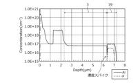
- FIG. 9 is a graph showing calculated values of the Al concentration profile in the p-type region of the SJ-MOSFET according to the embodiment.
- FIG. 10 is a graph showing calculated values of Al and P concentration profiles in the p-type region of the SJ-MOSFET according to the embodiment.
- FIG. 11 is a graph showing calculated values of Al and Ar concentration profiles in the p-type region of the SJ-MOSFET according to the embodiment.
- FIG. 12 shows the experimental results showing the fluctuation of the on-voltage of a conventional SJ-MOSFET.
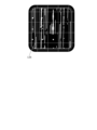
- FIG. 13 is a plan view showing a schematic diagram of the growth of stacking faults in a conventional SJ-MOSFET.
- a super junction silicon carbide semiconductor device is as follows.
- a first semiconductor layer of a first conductivity type is provided on a front surface of a silicon carbide semiconductor substrate of a first conductivity type.
- a parallel pn region in which first column regions of a first conductivity type and second column regions of a second conductivity type are repeatedly and alternately arranged in a plane parallel to the front surface is provided on a surface of the first semiconductor layer opposite to the silicon carbide semiconductor substrate.
- a second semiconductor layer of a second conductivity type is provided on a surface of the parallel pn region opposite to the silicon carbide semiconductor substrate.
- a first semiconductor region of a first conductivity type having a higher impurity concentration than the first semiconductor layer is selectively provided within the second semiconductor layer.
- a gate electrode is provided via a gate insulating film in contact with a part of the second semiconductor layer and a part of the first semiconductor region.
- a first electrode is provided in contact with the first semiconductor region and the second semiconductor layer.
- a second electrode is provided on a rear surface of the silicon carbide semiconductor substrate.
- a second semiconductor region of a second conductivity type is provided in the first semiconductor layer at a bottom surface of the second column region, in contact with the second column region and doped with an impurity of a second conductivity type.
- a concentration of the impurity of the second conductivity type has a concentration spike that decreases to 1/10 or less of a maximum concentration of the impurity of the second conductivity type in the second semiconductor region.
- ions of p-type impurities or the like are implanted into the bottom of the SJ trench, and defects are introduced into the drift layer (first semiconductor layer of the first conductivity type) by the ion implantation. These defects diffuse during epitaxial growth of the p-type epitaxial layer (third semiconductor layer of the second conductivity type) and spread into the drift layer, thereby reducing the lifetime of the drift layer. This makes it possible to suppress degradation of electrical conduction when the body diode is energized.
- the second semiconductor region may be a region in which the first semiconductor layer is doped with the second conductivity type impurity, the second conductivity type impurity and the first conductivity type impurity, or the second conductivity type impurity and a rare gas element.
- the second conductivity type impurity may be aluminum or boron
- the first conductivity type impurity may be phosphorus or nitrogen
- the rare gas element may be neon, argon, krypton, or xenon.
- the second semiconductor region may have a compensation concentration in the range of 1 ⁇ 10 16 /cm 3 to 1 ⁇ 10 17 /cm 3 inclusive, and the maximum concentration of the total of the implanted elements may be 2 ⁇ 10 17 /cm 3 or less.
- the second semiconductor region may have a thickness in the range of 0.1 ⁇ m to 1 ⁇ m.
- the gate electrode provided via the gate insulating film may be provided inside a trench that penetrates the first semiconductor region and the second semiconductor layer to reach the first semiconductor layer.
- the above disclosure makes it possible to prevent the loss of the p-type region implanted with ions by hydrogen etching during the epitaxial growth of the p-type epitaxial layer, and to introduce defects.
- a method for manufacturing a superjunction silicon carbide semiconductor device is as follows. First, a first step is performed in which a first semiconductor layer of a first conductivity type is formed on the front surface of a silicon carbide semiconductor substrate of a first conductivity type. Next, a second step is performed in which an SJ trench that does not reach the silicon carbide semiconductor substrate is formed from the surface of the first semiconductor layer opposite to the silicon carbide semiconductor substrate side. Next, a third step is performed in which a second semiconductor region of a second conductivity type is formed by ion-implanting impurities into the bottom of the SJ trench.
- a fourth step is performed in which a third semiconductor layer of a second conductivity type is epitaxially grown so as to fill the SJ trench.
- a fifth step is performed in which a surface of the third semiconductor layer is polished and the third semiconductor layer is left inside the SJ trench to form a parallel pn region in which a first column region of a first conductivity type and a second column region of a second conductivity type are repeatedly and alternately arranged in a plane parallel to the front surface on the surface of the first semiconductor layer opposite to the silicon carbide semiconductor substrate side.
- a sixth step is performed to form a second semiconductor layer of a second conductivity type on the surface of the parallel pn region opposite to the silicon carbide semiconductor substrate side.
- a seventh step is performed to selectively form a first semiconductor region of a first conductivity type having a higher impurity concentration than the first semiconductor layer inside the second semiconductor layer.
- an eighth step is performed to form a gate electrode via a gate insulating film that contacts a part of the second semiconductor layer and a part of the first semiconductor region.
- a ninth step is performed to form a first electrode that contacts the first semiconductor region and the second semiconductor layer.
- a tenth step is performed to form a second electrode on the back surface of the silicon carbide semiconductor substrate.
- the impurity may be a second conductivity type impurity, a second conductivity type impurity and a first conductivity type impurity, or a second conductivity type impurity and a rare gas element.
- the eighth step may also include forming a trench penetrating the first semiconductor region and the second semiconductor layer to reach the first semiconductor layer, and forming a gate electrode inside the trench via a gate insulating film.
- the problems of conventional super-junction silicon carbide semiconductor devices will be described.
- the n-type conduction layer (drift layer) is the semiconductor layer with the highest resistance.
- the electrical resistance of this n-type drift layer has a large effect on the on-resistance of the entire vertical MOSFET.
- the thickness of the n-type drift layer can be reduced to shorten the current path.
- the depletion layer extends to the highly resistive n-type drift layer in the off state, so that the vertical MOSFET also has the function of maintaining the breakdown voltage. Therefore, if the n-type drift layer is made thinner to reduce the on-resistance, the depletion layer in the off state is shortened, so that the breakdown field strength is easily reached at a low applied voltage, and the breakdown voltage is reduced.
- the thickness of the n-type drift layer must be increased, and the on-resistance increases. This relationship between on-resistance and breakdown voltage is called a trade-off relationship, and it is generally difficult to improve both of these trade-off relationships. It is known that this trade-off relationship between on-resistance and breakdown voltage also exists in semiconductor devices such as IGBTs (Insulated Gate Bipolar Transistors), bipolar transistors, and diodes.
- the super junction (SJ) structure is known as a semiconductor device structure that solves the problems described above (see Patent Documents 3 and 4 mentioned above).
- a MOSFET having a superjunction structure (hereinafter, SJ-MOSFET) is made of a wafer in which an n-type buffer layer and an n-type drift layer are grown on a highly doped n + -type silicon carbide semiconductor substrate.
- a p-type column region is provided that penetrates the n-type drift layer from the surface of the wafer and does not reach the n + -type silicon carbide semiconductor substrate.
- the p-type column region may not reach the n + -type silicon carbide semiconductor substrate, or may reach the n + -type silicon carbide semiconductor substrate.
- the n-type drift layer has a parallel structure (hereinafter referred to as a parallel pn structure) in which p-type regions (p-type column regions) and n-type regions (portions of the n-type drift layer sandwiched between p-type column regions, hereinafter referred to as n-type column regions) that extend in a direction perpendicular to the substrate main surface and have a narrow width in a plane parallel to the substrate main surface are alternately arranged in a plane parallel to the substrate main surface.
- the parallel pn structure may also be called a parallel pn region.
- the p-type column region and n-type column region that make up the parallel pn structure are regions with a high impurity concentration corresponding to the n-type drift layer.
- the amount of impurities which is the product of the impurity concentration and area contained in the p-type column region and the n-type column region, are approximately equal in charge balance, thereby expanding the depletion layer in the off state to maintain the breakdown voltage, and it is possible to achieve both low on-resistance and breakdown voltage due to the high impurity concentration.
- FIG. 12 is an experimental result showing the fluctuation of the on-voltage of a conventional SJ-MOSFET.
- the horizontal axis indicates the current stress of the body diode in A/cm 2.
- the vertical axis indicates the rate of fluctuation of the on-voltage from the initial value in %, in %.
- multiple measurement points e.g., black squares
- the same structure e.g., a non-SJ structure
- the same current stress value e.g., 500 A/cm 2
- FIG. 13 is a plan view of an element showing the growth of stacking faults in a conventional SJ-MOSFET formed by the trench backfilling method, and is the experimental result of peeling off the surface electrode of an element in which the on-voltage fluctuated, and performing a PL (photoluminescence) mapping measurement at the emission wavelength (420 nm) of stacking faults.
- PL photoluminescence
- This degradation due to the stacking faults is a phenomenon unique to silicon carbide semiconductors.
- the rate of fluctuation of the on-voltage is larger in the trench backfilling ( ⁇ mark) than in the multi-epi implantation ( ⁇ mark).
- ⁇ mark the trench backfilling
- ⁇ mark the multi-epi implantation
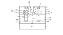
- FIG. 1 is a cross-sectional view showing a cross-sectional structure of an SJ-MOSFET according to an embodiment.
- the super-junction silicon carbide semiconductor device according to the present disclosure will be described using an SJ-MOSFET 50 as an example.
- the SJ-MOSFET 50 shown in FIG. 1 is an SJ-MOSFET 50 equipped with a MOS (Metal Oxide Semiconductor) gate on the front surface (surface on the p-type base layer 6 side described later) of a semiconductor substrate (silicon carbide substrate: semiconductor chip) made of silicon carbide.
- MOS Metal Oxide Semiconductor
- a drift layer 64 is provided on a first main surface (front surface), for example, a (0001) surface (Si surface) of an n + type silicon carbide substrate (a silicon carbide semiconductor substrate of a first conductivity type) 1.
- the n + type silicon carbide substrate 1 is, for example, a silicon carbide single crystal substrate doped with nitrogen (N).
- the drift layer 64 includes an n type buffer layer (a first semiconductor layer of a first conductivity type) 17 that becomes a bulk drift layer 61, and an SJ structure 62 provided on the front surface of the n type buffer layer 17.
- the SJ structure 62 includes a p type column region 3 and an n type column region 4.
- An n-type high concentration region 5 is selectively provided in a surface layer of the n-type column region 4 on the side opposite to the n + type silicon carbide substrate 1.
- the n-type high concentration region 5 is a high concentration n -type drift layer having an impurity concentration lower than that of the n + type silicon carbide substrate 1 and higher than that of the n-type column region 4.
- the n-type high concentration region 5 is a so-called current spreading layer (CSL) that reduces the spreading resistance of carriers.
- a p-type base layer (second semiconductor layer of second conductivity type) 6 is provided on the surface side of the drift layer 64 opposite to the n + type silicon carbide substrate 1 side.
- the n + type silicon carbide substrate 1, bulk drift layer 61, SJ structure 62, n-type high concentration region 5, and p-type base layer 6 will be collectively referred to as a silicon carbide semiconductor base.
- the n-type buffer layer 17 is bulk drift layer 61 having a thickness of about 4.4 ⁇ m and an impurity concentration of about 1.8 ⁇ 10 16 /cm 3 .
- a parallel pn structure 21 that becomes an SJ structure 62 is provided in the drift layer 64 of the SJ-MOSFET 50.
- n-type column regions (first columns of a first conductivity type) 4 and p-type column regions (second columns of a second conductivity type) 3 are alternately and repeatedly arranged in a plane parallel to the front surface of the n + -type silicon carbide substrate 1.
- the n-type column regions 4 are provided so as to reach the n-type high concentration region 5 from the surface of the n-type buffer layer 17.
- the p-type column regions 3 have an impurity concentration of about 6 ⁇ 10 16 /cm 3
- the n-type column regions 4 have an impurity concentration of about 3 ⁇ 10 16 /cm 3.
- the solid line (boundary line) between the n-type buffer layer 17 and the n-type column regions 4 means that the n-type impurity concentration of the n-type column regions 4 is higher than that of the n-type buffer layer 17.
- the n-type buffer layer 17 and the n-type column region 4 may be formed of epitaxially grown layers doped with n-type impurities at the same concentration. In this case, the boundary between the n-type buffer layer 17 and the n-type column region 4 is not necessary.
- the p-type region 19 introduces defects (crystal defects, ion implantation damage) due to ion implantation formed in the drift layer 64.
- defects crystal defects, ion implantation damage
- the SJ structure 62 is formed, these crystal defects diffuse during epitaxial growth when the next p-type epitaxial layer 22 (see FIG. 6) is formed, and spread to at least a part of the drift layer 64 centered on the p-type region 19, thereby reducing the lifetime of the drift layer 64. It is particularly important to reduce the lifetime of the n-type buffer layer 17 and the n-type column region 4 adjacent to the p-type region 19. This makes it possible to suppress deterioration of the conduction of electricity when the body diode is conducting.
- the depth of the SJ trench 24 can be made shallower, so that the etching time of the SJ trench 24 and the time to fill the SJ trench 24 with the p-type epitaxial layer 22 can be shortened. This is expected to reduce the cost of the process.
- silicon carbide semiconductors even if heat treatment is performed after ion implantation of impurities that act as dopants, the impurities themselves hardly diffuse, but it has been observed that crystal defects (lattice defects) formed by ion implantation diffuse due to heat treatment. Note that Figure 1 does not show the defects caused by ion implantation or their distribution after diffusion.
- the product of the width of the p-type column region 3 and the impurity concentration of the p-type column region 3 is approximately equal to the product of the width of the n-type column region 4 and the impurity concentration of the n-type column region 4 (amount of impurities). Specifically, this is within ⁇ 5%.
- the parallel pn structure 21 is known as a structure that simultaneously obtains both low on-resistance and high withstand voltage characteristics.
- a drain electrode (second electrode) 18 is provided on a second main surface (back surface, i.e., the back surface of the silicon carbide semiconductor base) of the n + type silicon carbide substrate 1.
- a drain electrode pad (not shown) is provided on the surface of the drain electrode 18.
- a trench structure is formed on the first main surface side (p-type base layer 6 side) of the silicon carbide semiconductor substrate.
- the SJ-MOSFET 50 has a MOS structure 63 consisting of an n-type high concentration region 5, a p-type base layer 6, an n + -type source region 7, a p + -type contact region 8, a gate insulating film 9, a gate electrode 10, and a trench 16.
- the trench 16 penetrates the p-type base layer 6 from the surface of the p-type base layer 6 opposite to the n + -type silicon carbide substrate 1 side (the first main surface side of the silicon carbide semiconductor substrate) to reach the n-type high concentration region 5.
- a gate insulating film 9 is formed on the bottom and side walls of the trench 16 along the inner wall of the trench 16, and a gate electrode 10 is formed inside the gate insulating film 9 in the trench 16.
- the gate electrode 10 is insulated from the n-type high concentration region 5 and the p-type base layer 6 by the gate insulating film 9. A part of the gate electrode 10 may protrude from above the trench 16 to the source electrode 12 side described later.
- a first p + -type base region 14 and a second p + -type base region 15 are selectively provided inside the n-type high concentration region 5.
- the first p + -type base region 14 covers at least the bottom surface of the trench 16 and the bottom corner portion.
- the bottom corner portion of the trench 16 is the boundary between the bottom surface and the side wall of the trench 16.
- the second p + -type base region 15 is provided between the trenches 16, and is provided from the surface of the n-type high concentration region 5 on the p-type base layer 6 side to the same depth as the first p + -type base region 14.
- the pn junctions between the first p + -type base region 14 and the second p + -type base region 15 and the n-type column region 4 are formed at positions deeper on the drain side than the bottom surface of the trench 16.
- the depth positions of the drain side ends of the first p + -type base region 14 and the second p + -type base region 15 may be changed in various ways according to design conditions as long as the pn junctions between the first p + -type base region 14 and the second p + -type base region 15 and the n-type column region 4 are positioned deeper on the drain side than the bottom surface of the trench 16.
- the first p + -type base region 14 and the second p + -type base region 15 can prevent a high electric field from being applied to the gate insulating film 9 in the portion along the bottom surface of the trench 16.
- an n + -type source region (first semiconductor region of a first conductivity type) 7 is selectively provided on the first main surface side of the substrate.
- a p + -type contact region 8 may also be provided.
- the n + -type source region 7 is in contact with the trench 16.
- the n + -type source region 7 and the p + -type contact region 8 are in contact with each other.
- the front surface refers to the first main surface of the n + -type silicon carbide substrate 1, for example, the (0001) surface (Si surface), and "provided on the surface of the semiconductor layer” refers to a semiconductor region/semiconductor layer being provided above the surface of the semiconductor layer, and "provided on the surface layer of the semiconductor layer” refers to a semiconductor region/semiconductor layer being provided inside the semiconductor layer and exposed to the surface of the semiconductor layer.
- the interlayer insulating film 11 is provided on the entire surface of the first main surface side of the silicon carbide semiconductor substrate so as to cover the gate electrode 10 embedded in the trench 16.
- the source electrode 12 contacts the n + type source region 7 and the p type base layer 6 through a contact hole opened in the interlayer insulating film 11.
- the source electrode 12 contacts the n + type source region 7 and the p + type contact region 8.
- the source electrode 12 is made of, for example, a NiSi film.
- the source electrode 12 is electrically insulated from the gate electrode 10 by the interlayer insulating film 11.
- a source electrode pad (not shown) made of Al or AlSi is provided on the source electrode 12.
- a barrier metal (not shown) made of, for example, Ti and TiN that prevents diffusion of metal atoms from the source electrode 12 to the gate electrode 10 may be provided between the source electrode 12 and the interlayer insulating film 11.
- the body diode of the SJ-MOSFET which is the subject of the problem, is a parasitic pn diode between the p-type base layer 6 and the n-type high concentration region 5.
- the p-type base layer 6 is connected to the source electrode 12 via the p + type contact region 8.
- the n-type high concentration region 5 is connected to the drain electrode 18 via the n-type column region 4, the n-type buffer layer 17, and the n + type silicon carbide substrate 1.
- the reflux mode of the SJ-MOSFET when the potential of the source electrode 12 becomes higher than that of the drain electrode 18 and exceeds the threshold voltage of the body diode, the body diode is energized and carriers are injected.
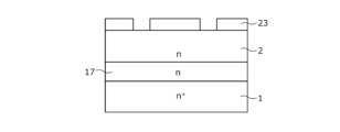
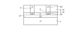
- Figures 2 to 8 are cross-sectional views each showing a schematic state during the manufacturing process of the super junction silicon carbide semiconductor device according to the embodiment.
- an n + type silicon carbide substrate 1 made of n type single crystal 4H-SiC is prepared.
- an n type buffer layer 17 and an n type drift layer 2 are epitaxially grown in this order on a first main surface of the n + type silicon carbide substrate 1.
- the n type buffer layer 17 and the n type drift layer 2 are assumed to be elements having slightly different n type impurity concentrations. The state up to this point is shown in FIG.
- a SiO 2 mask 23 having predetermined openings and serving as a trench etching mask is formed by photolithography on the surface of the n-type drift layer 2. The state up to this point is shown in FIG.
- an SJ trench 24 is formed by dry etching in the n-type drift layer 2, the SJ trench 24 having a depth approximately equal to the film thickness of the n-type drift layer 2 and not reaching the n + -type silicon carbide substrate 1. The state up to this point is shown in FIG.
- p-type impurities are ion-implanted into the bottom of the SJ trench 24 to form a p-type region 19.
- crystal defects due to ion implantation are introduced into the n-type buffer layer 17.
- the state up to this point is shown in FIG. 5.
- the elements to be ion-implanted are, for example, Al, Al and n-type impurities (phosphorus (P), nitrogen (N), etc.), and Al and rare gas elements (neon (Ne), argon (Ar), krypton (Kr), xenon (Xe), etc.).
- the concentration of the ion-implanted elements can be made higher than in the case of Al alone, and the amount of defects can be increased.
- Boron (B) may be used as a p-type impurity instead of Al.
- B alone, B and n-type impurities, or B and rare gas elements may also be ion-implanted.
- the ion implantation temperature is preferably performed at room temperature so as not to restore crystal defects due to ion implantation during implantation.
- the compensation concentration of p-type region 19 (the difference in concentration between p-type impurities and n-type impurities) is within the same range of impurity concentration as that of p-type epitaxial layer 22 formed below (1 ⁇ 10 16 /cm 3 to 1 ⁇ 10 17 /cm 3 ), and the maximum total concentration of the ion-implanted elements is 2 ⁇ 10 17 /cm 3 or less. If the compensation concentration of p-type region 19 is higher than this, the JFET resistance will increase, and if it is lower than this, there will be fewer defects due to ion implantation, and the effect of suppressing degradation due to electrical conduction will be reduced.
- the thickness of the p-type region 19 is preferably within the range of 0.1 ⁇ m to 1 ⁇ m. If the p-type region 19 is thinner than this, it will be lost by hydrogen etching during the subsequent epitaxial growth of the p-type epitaxial layer 22, and if it is thicker than this, highly accelerated ion implantation will be required, which will increase the cost of implantation.
- a p-type epitaxial layer 22 made of silicon carbide is epitaxially grown on the front surface side of the n-type buffer layer 17 while doping with p-type impurities such as aluminum, and the SJ trench 24 is backfilled with the p-type epitaxial layer 22.
- the impurity concentration of the p-type epitaxial layer 22 is in the range of 1 ⁇ 1016 to 1 ⁇ 1017 /cm3. The state up to this point is shown in FIG .
- Crystal defects caused by ion implantation diffuse during epitaxial growth and spread into the n-type buffer layer 17, reducing the lifetime of the drift layer and suppressing degradation of electrical conductivity when the body diode is energized.
- this p-type epitaxial layer 22 is polished, leaving the p-type epitaxial layer 22 inside the SJ trench 24, thereby forming a parallel pn structure 21 consisting of p-type column regions 3 and n-type column regions 4.
- the p-type epitaxial layer 22 inside the SJ trench 24 becomes the p-type column regions 3, and the region of the n-type drift layer 2 sandwiched between the p-type column regions 3 becomes the n-type column regions 4. This is the meaning behind 2 ⁇ 4 in Figure 7. The state up to this point is shown in Figure 7.
- the lower n-type high concentration region 5a made of silicon carbide is epitaxially grown on the front surface side of the n-type drift layer 2 while doping with nitrogen atoms.
- the lower second p + type base region 15a is formed by selective ion implantation.
- the upper n-type high concentration region 5b made of silicon carbide is epitaxially grown thereon while doping with nitrogen atoms.
- the upper second p + type base region 15b is formed by selective ion implantation.
- the lower n-type high concentration region 5a and the upper n-type high concentration region 5b form the n-type high concentration region 5.
- the lower second p + type base region 15a and the upper second p + type base region 15b form the second p + type base region 15.
- a p-type base layer 6 doped with p-type impurities such as aluminum is formed on the surface of the n-type high concentration region 5.
- an ion implantation mask having a predetermined opening is formed, for example, of an oxide film, on the surface of the p-type base layer 6 by photolithography.
- An n-type impurity such as phosphorus (P) is ion-implanted into this opening to form an n + -type source region 7 in a part of the surface of the p-type base layer 6.
- the ion implantation mask used for forming the n + -type source region 7 is removed, and an ion implantation mask having a predetermined opening is formed in the same manner, and a p-type impurity such as aluminum is ion-implanted into a part of the surface of the p-type base layer 6 to form a p + -type contact region 8.
- the impurity concentration of the p + -type contact region 8 is set to be higher than the impurity concentration of the p-type base layer 6.
- a heat treatment is performed in an inert gas atmosphere at about 1700° C. to activate the first p + type base region 14, the second p + type base region 1, the n + type source region 7, the p + type contact region 8, etc.
- the ion implantation regions may be activated collectively by a single heat treatment, or the heat treatment may be performed each time an ion implantation is performed.
- a trench forming mask having a predetermined opening is formed on the surface of the p-type base layer 6 by photolithography, for example, using an oxide film.
- a trench 16 is formed by dry etching, penetrating the p-type base layer 6 and reaching the n-type high concentration region 5. The bottom of the trench 16 may reach the first p + -type base region 14 formed in the n-type high concentration region 5.
- the trench forming mask is removed. The state up to this point is shown in FIG. 8.
- a gate insulating film 9 is formed along the surface of the n + -type source region 7 and the bottom and sidewalls of the trench 16.
- This gate insulating film 9 may be formed by thermal oxidation at a temperature of about 1000° C. in an oxygen atmosphere.
- this gate insulating film 9 may be formed by a method of deposition by a chemical reaction such as high temperature oxidation (HTO).
- a polycrystalline silicon layer doped with, for example, phosphorus atoms is provided on the gate insulating film 9.
- This polycrystalline silicon layer may be formed so as to fill the trench 16.
- This polycrystalline silicon layer is patterned by photolithography and left inside the trench 16 to form the gate electrode 10.
- phosphorus glass is deposited to a thickness of about 1 ⁇ m so as to cover the gate insulating film 9 and the gate electrode 10, forming the interlayer insulating film 11.
- a barrier metal (not shown) made of titanium (Ti) or titanium nitride (TiN) may be formed so as to cover the interlayer insulating film 11.
- the interlayer insulating film 11 and the gate insulating film 9 are patterned by photolithography to form a contact hole exposing the n + type source region 7.
- the n + type source region 7 and a contact hole exposing the n + type source region 7 are formed.
- a conductive film (not shown) is provided in the contact holes and on the interlayer insulating film 11. This conductive film is selectively removed to leave the conductive film only in the contact holes, and the n + type source region 7 and the conductive film are brought into contact with each other.
- the p + type contact region 8 is formed, the n + type source region 7 and the p + type contact region 8 are brought into contact with the conductive film.
- the conductive film may be, for example, nickel silicide.
- a source electrode 12 made of aluminum or the like is provided.
- a back electrode made of nickel or the like is provided on the second main surface of the n + type silicon carbide semiconductor substrate 1.
- a heat treatment is performed in an inert gas atmosphere at about 1000° C. to form a drain electrode 18 that forms an ohmic junction with the n + type silicon carbide semiconductor substrate 1.
- an electrode pad that will become a source electrode pad (not shown) for soldering a terminal is deposited on the source electrode 12 on the front surface of the silicon carbide semiconductor substrate and on the interlayer insulating film 11, for example by sputtering. In this manner, the super-junction silicon carbide semiconductor device shown in FIG. 1 is completed.
- an n-type well region is formed in a part of the surface region of p-type base layer 6, the front surface side of the silicon carbide semiconductor substrate is thermally oxidized to form a gate insulating film 9, the p-type base layer 6 and each region formed on the surface of the p-type base layer 6 are covered with the gate insulating film 9, a polycrystalline silicon layer is formed as gate electrode 10 on the gate insulating film 9, the polycrystalline silicon layer is patterned and selectively removed, the polycrystalline silicon layer is left on a portion of the p-type base layer 6 sandwiched between the n + -type source region 7 and the n-type well region, and an interlayer insulating film 11 is formed so as to cover the gate electrode 7.
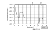
- FIG. 9 is a graph showing the results of simulating (Monte Carlo method) the Al concentration profile of the p-type region of the SJ-MOSFET according to the embodiment.
- the horizontal axis indicates the depth from the surface of the p + -type contact region 8 in ⁇ m.
- the vertical axis indicates the Al impurity concentration in cm ⁇ 3 .
- concentration spike As shown in FIG. 9, at the boundary between the p-type column region 3 and the p-type region 19, there is a concentration spike where the Al impurity concentration drops sharply to about 2 ⁇ 10 15 /cm 3.
- the Al impurity concentration is 1/10 or less of the maximum Al concentration of the p-type region 19 (about 8 ⁇ 10 16 /cm 3 in this example).
- This is a structural feature associated with the manufacturing method of the SJ-MOSFET according to the embodiment, and is because when ions are implanted into the trench bottom, the concentration at the top surface of the trench bottom is low due to the influence of the ion implantation range.
- the impurity concentrations of the p-type column region 3 and the p-type region 19 are approximately the same, ie, 1 ⁇ 10 16 /cm 3 or more and 1 ⁇ 10 17 /cm 3 or less.
- FIG. 10 is a graph showing the results of simulating the Al and P concentration profiles of the p-type region of the SJ-MOSFET according to the embodiment.
- the horizontal axis indicates the depth from the surface of the p + -type contact region 8 in ⁇ m.
- the vertical axis indicates the impurity concentrations of Al and P in cm ⁇ 3 .
- concentration spike where the Al impurity concentration suddenly decreases to about 2 ⁇ 10 15 /cm 3. That is, in FIG. 10, as in FIG.
- the compensation concentration of the p-type column region 3 and the impurity concentration of the p-type region 19 are approximately the same, at 1 ⁇ 10 16 /cm 3 or more and 1 ⁇ 10 17 /cm 3 or less.
- the maximum total concentration of the ion-implanted elements is 2 ⁇ 10 17 /cm 3 or less.
- Fig. 10 shows an example of P, but the same applies to the case of N.
- FIG. 11 is a graph showing the results of simulating the Al and Ar concentration profiles of the p-type region of the SJ-MOSFET according to the embodiment.
- the horizontal axis indicates the depth from the surface of the p + -type contact region 8 in ⁇ m.
- the vertical axis indicates the impurity concentrations of Al and Ar in cm ⁇ 3 .
- concentration spike where the Al impurity concentration suddenly decreases to about 2 ⁇ 10 15 /cm 3. That is, in FIG. 11, as in FIG.
- the impurity concentrations of the p-type column region 3 and the p-type region 19 are approximately the same, 1 ⁇ 10 16 /cm 3 or more and 1 ⁇ 10 17 /cm 3 or less.
- the maximum total concentration of the ion-implanted elements is 2 ⁇ 10 17 /cm 3 or less.
- Fig. 11 shows an example of Ar, but the same applies to the cases of other inert elements (Ne, Kr, Xe).
- the super junction silicon carbide semiconductor device and the method of manufacturing the super junction silicon carbide semiconductor device of the embodiment after the SJ trench is formed, ion implantation of p-type impurities or the like is performed at the bottom of the SJ trench, and defects due to ion implantation are introduced into the drift layer. These crystal defects diffuse during epitaxial growth of the p-type epitaxial layer and spread to at least a part of the drift layer, thereby reducing the lifetime of the drift layer. As a result, it is possible to suppress deterioration of electrical conductivity when the body diode is energized.
- a structural feature obtained by ion implantation of p-type impurities or the like at the bottom of the SJ trench corresponds to a concentration spike at the boundary between the p-type column region 3 and the p-type region 19, where the Al impurity concentration is 1/10 or less of the maximum Al concentration in the p-type region 19.
- the suppression of the deterioration of the body diode due to the conduction of current is described in detail below.
- the crystal defects in the p-type region 19 formed by ion implantation also diffuse into the adjacent n-type buffer layer 17 and n-type column region 4, shortening the carrier lifetime of these regions.
- the main cause of the deterioration of the body diode due to the conduction of current is that when holes, which are minority carriers, reach the n + type silicon carbide substrate 1 and reach a certain density or more, the stacking faults (basal plane dislocations) remaining in the n + type silicon carbide substrate 1 are expanded by the energy generated when the holes are recombined with electrons.
- the present disclosure has been described by taking as an example a case where the main surface of a silicon carbide substrate made of silicon carbide is a (0001) surface and a MOS is constructed on the (0001) surface, but the present disclosure is not limited to this, and the wide band gap semiconductor, the surface orientation of the substrate main surface, and the like can be variously changed.
- a trench MOSFET has been described as an example, but the present disclosure is not limited to this, and the present disclosure can be applied to semiconductor devices of various configurations, such as MOS type semiconductor devices such as planar MOSFETs.
- the drift layer 64 is composed of a bulk drift layer 61 and an SJ structure 62.
- the bulk drift layer 61 may be omitted, and a full SJ structure in which the bottom surface of the p-type region 19 is in contact with the n + -type silicon carbide substrate 1 may be adopted.
- the super-junction silicon carbide semiconductor device and the method for manufacturing the super-junction silicon carbide semiconductor device disclosed herein are useful for high-voltage semiconductor devices used in power conversion devices and power supply devices for various industrial machines, etc.
Landscapes
- Electrodes Of Semiconductors (AREA)
Abstract
超接合炭化珪素半導体装置は、炭化珪素半導体基板(1)と、第1導電型の第1半導体層(17)と、第1導電型の第1カラム領域(4)と第2導電型の第2カラム領域(3)とが繰り返し交互に配置された並列pn領域(21)と、第1導電型の第2半導体層(5)と、第1導電型の第1半導体領域(7)と、トレンチ(16)と、ゲート電極(10)と、第1電極(12)と、第2電極(18)と、を備える。第2カラム領域(3)の底面に、第2カラム領域(3)と接し、第2導電型の不純物が添加された第2導電型の第2半導体領域(19)が第1半導体層(1)内に設けられる。第2半導体領域(19)と第2カラム領域(3)の境界において、第2導電型の不純物の濃度は、第2半導体領域(19)の第2導電型の不純物の最大濃度に対して、1/10以下に減少する濃度スパイクを有する。
Description
この開示は、超接合炭化珪素半導体装置および超接合炭化珪素半導体装置の製造方法に関する。
特許文献1には、シリコン半導体のMOSFET半導体装置において、トレンチ内に逆導電型半導体層を埋め込んで、超接合構造を形成する技術が記載されている。より具体的には、一導電型半導体層に比較的浅いトレンチを形成し、トレンチ底部に逆導電型不純物領域を形成し、トレンチ内に逆導電型半導体層を埋め込んで、超接合構造の基板を形成し、当該基板表面に少なくとも1つのpn接合を有する素子領域を形成する技術が記載されている。特許文献2にも同様な技術が記載されている。
特許文献3には、炭化珪素半導体のMOSFET半導体装置において、比較的薄いエピタキシャル成長層を形成し、その層に逆導電型となるようドーパントを選択的にイオン注入することを繰り返し行う、マルチエピインプラ法によるスーパージャンクション構造の形成技術が記載されている。
特許文献4には、炭化珪素半導体のMOSFET半導体装置において、比較的厚いエピタキシャル成長層に深いトレンチを形成し、そのトレンチ内に逆導電型の半導体層を埋め込む、トレンチ埋め戻し法によるスーパージャンクション構造の形成技術が記載されている。
この開示は、MOSFET内に寄生的に形成されるボディダイオード通電時の通電劣化を抑制し、プロセスコストを低減できる超接合炭化珪素半導体装置および超接合炭化珪素半導体装置の製造方法を提供することを目的とする。
この開示の一態様にかかる超接合炭化珪素半導体装置は、以下の通りである。第1導電型の炭化珪素半導体基板のおもて面に第1導電型の第1半導体層が設けられる。前記第1半導体層の、前記炭化珪素半導体基板側に対して反対側の表面に、第1導電型の第1カラム領域と第2導電型の第2カラム領域とが前記おもて面に平行な面において繰り返し交互に配置された並列pn領域が設けられる。前記並列pn領域の、前記炭化珪素半導体基板側に対して反対側の表面に第2導電型の第2半導体層が設けられる。前記第2半導体層の内部に選択的に前記第1半導体層よりも不純物濃度の高い第1導電型の第1半導体領域が設けられる。前記第2半導体層の一部と前記第1半導体領域の一部に接するゲート絶縁膜を介してゲート電極が設けられる。前記第1半導体領域および前記第2半導体層に接する第1電極が設けられる。前記炭化珪素半導体基板の裏面に第2電極が設けられる。前記第2カラム領域の底面に、前記第2カラム領域と接し、第2導電型の不純物が添加された第2導電型の第2半導体領域が前記第1半導体層内に設けられる。前記第2半導体領域と前記第2カラム領域の境界において、前記第2導電型の不純物の濃度は、前記第2半導体領域の前記第2導電型の不純物の最大濃度に対して、1/10以下に減少する濃度スパイクを有する。
本開示にかかる超接合炭化珪素半導体装置および超接合炭化珪素半導体装置の製造方法によれば、ボディダイオード通電時の通電劣化を抑制し、プロセスコストを低減できるという効果を奏する。
<本開示の実施形態の概要>
(1)この開示の一態様にかかる超接合炭化珪素半導体装置は、以下の通りである。第1導電型の炭化珪素半導体基板のおもて面に第1導電型の第1半導体層が設けられる。前記第1半導体層の、前記炭化珪素半導体基板側に対して反対側の表面に、第1導電型の第1カラム領域と第2導電型の第2カラム領域とが前記おもて面に平行な面において繰り返し交互に配置された並列pn領域が設けられる。前記並列pn領域の、前記炭化珪素半導体基板側に対して反対側の表面に第2導電型の第2半導体層が設けられる。前記第2半導体層の内部に選択的に前記第1半導体層よりも不純物濃度の高い第1導電型の第1半導体領域が設けられる。前記第2半導体層の一部と前記第1半導体領域の一部に接するゲート絶縁膜を介してゲート電極が設けられる。前記第1半導体領域および前記第2半導体層に接する第1電極が設けられる。前記炭化珪素半導体基板の裏面に第2電極が設けられる。前記第2カラム領域の底面に、前記第2カラム領域と接し、第2導電型の不純物が添加された第2導電型の第2半導体領域が前記第1半導体層内に設けられる。前記第2半導体領域と前記第2カラム領域の境界において、前記第2導電型の不純物の濃度は、前記第2半導体領域の前記第2導電型の不純物の最大濃度に対して、1/10以下に減少する濃度スパイクを有する。
(1)この開示の一態様にかかる超接合炭化珪素半導体装置は、以下の通りである。第1導電型の炭化珪素半導体基板のおもて面に第1導電型の第1半導体層が設けられる。前記第1半導体層の、前記炭化珪素半導体基板側に対して反対側の表面に、第1導電型の第1カラム領域と第2導電型の第2カラム領域とが前記おもて面に平行な面において繰り返し交互に配置された並列pn領域が設けられる。前記並列pn領域の、前記炭化珪素半導体基板側に対して反対側の表面に第2導電型の第2半導体層が設けられる。前記第2半導体層の内部に選択的に前記第1半導体層よりも不純物濃度の高い第1導電型の第1半導体領域が設けられる。前記第2半導体層の一部と前記第1半導体領域の一部に接するゲート絶縁膜を介してゲート電極が設けられる。前記第1半導体領域および前記第2半導体層に接する第1電極が設けられる。前記炭化珪素半導体基板の裏面に第2電極が設けられる。前記第2カラム領域の底面に、前記第2カラム領域と接し、第2導電型の不純物が添加された第2導電型の第2半導体領域が前記第1半導体層内に設けられる。前記第2半導体領域と前記第2カラム領域の境界において、前記第2導電型の不純物の濃度は、前記第2半導体領域の前記第2導電型の不純物の最大濃度に対して、1/10以下に減少する濃度スパイクを有する。
上述した開示によれば、SJトレンチ形成後に、SJトレンチ底に、p型の不純物等のイオン注入が行われ、ドリフト層(第1導電型の第1半導体層)にイオン注入による欠陥が導入される。この欠陥が、p型エピタキシャル層(第2導電型の第3半導体層)のエピタキシャル成長時に拡散し、ドリフト層に広がることで、ドリフト層のライフタイムを低下させることができる。このため、ボディダイオード通電時の通電劣化を抑制することができる。
(2)また、上述した(1)において、前記第2半導体領域は、前記第1半導体層に、前記第2導電型の不純物、前記第2導電型の不純物と第1導電型の不純物、または前記第2導電型の不純物と希ガス元素を注入した領域としてもよい。
(3)また、上述した(2)において、前記第2導電型の不純物は、アルミニウムまたはホウ素であり、前記第1導電型の不純物は、リンまたは窒素であり、前記希ガス元素は、ネオン、アルゴン、クリプトンまたはキセノンとしてもよい。
(4)また、上述した(1)~(3)のいずれか一つにおいて、前記第2半導体領域は、補償濃度が1×10¹⁶/cm3以上1×1017/cm3以下の範囲内であり、注入された元素の合計の最大濃度は2×1017/cm3以下としてもよい。
(5)また、上述した(1)~(4)のいずれか一つにおいて、前記第2半導体領域は、厚みが0.1μm以上1μm以下の範囲内としてもよい。
(6)また、上述した(1)において、前記ゲート絶縁膜を介して設けられた前記ゲート電極が、前記第1半導体領域および前記第2半導体層を貫通して前記第1半導体層に達するトレンチの内部に設けられるとしてもよい。
上述した開示によれば、p型エピタキシャル層のエピタキシャル成長の際に水素エッチングでイオン注入したp型領域が消失してしまうことを防ぎ、欠陥を導入することができる。
(7)この開示の一態様にかかる超接合炭化珪素半導体装置の製造方法は、以下の通りである。まず、第1導電型の炭化珪素半導体基板のおもて面に第1導電型の第1半導体層を形成する第1工程を行う。次に、前記第1半導体層の、前記炭化珪素半導体基板側に対して反対側の表面から、前記炭化珪素半導体基板に達しないSJトレンチを形成する第2工程を行う。次に、前記SJトレンチの底に、不純物をイオン注入することにより、第2導電型の第2半導体領域を形成する第3工程を行う。次に、前記SJトレンチを埋め込むように第2導電型の第3半導体層をエピタキシャル成長させる第4工程を行う。次に、前記第3半導体層の表面を研磨し、前記第3半導体層を前記SJトレンチ内部に残すことにより、前記第1半導体層の、前記炭化珪素半導体基板側に対して反対側の表面に、第1導電型の第1カラム領域と第2導電型の第2カラム領域とが前記おもて面に平行な面において繰り返し交互に配置された並列pn領域を形成する第5工程を行う。次に、前記並列pn領域の、前記炭化珪素半導体基板側に対して反対側の表面に第2導電型の第2半導体層を形成する第6工程を行う。次に、前記第2半導体層の内部に選択的に前記第1半導体層よりも不純物濃度の高い第1導電型の第1半導体領域を形成する第7工程を行う。次に、前記第2半導体層の一部と前記第1半導体領域の一部に接するゲート絶縁膜を介してゲート電極を形成する第8工程を行う。次に、前記第1半導体領域および前記第2半導体層に接する第1電極を形成する第9工程を行う。次に、前記炭化珪素半導体基板の裏面に第2電極を形成する第10工程を行う。
(8)また、上述した(7)において、前記不純物は、第2導電型の不純物、第2導電型の不純物と第1導電型の不純物または第2導電型の不純物と希ガス元素としてもよい。
(9)また、上述した(7)において、前記第8工程は、前記第1半導体領域および前記第2半導体層を貫通して、前記第1半導体層に達するトレンチを形成し、前記トレンチの内部にゲート絶縁膜を介してゲート電極を形成するとしてもよい。
<本開示の基礎となる知見>
最初に、従来の超接合炭化珪素半導体装置の課題について説明する。通常のn型チャネル縦型MOSFETでは、半導体基板内に形成される複数の半導体層のうち、n型伝導層(ドリフト層)が最も高抵抗の半導体層である。このn型ドリフト層の電気抵抗が縦型MOSFET全体のオン抵抗に大きく影響を与えている。縦型MOSFET全体のオン抵抗を低減するためには、n型ドリフト層の厚みを薄くし電流経路を短くすることで実現できる。
最初に、従来の超接合炭化珪素半導体装置の課題について説明する。通常のn型チャネル縦型MOSFETでは、半導体基板内に形成される複数の半導体層のうち、n型伝導層(ドリフト層)が最も高抵抗の半導体層である。このn型ドリフト層の電気抵抗が縦型MOSFET全体のオン抵抗に大きく影響を与えている。縦型MOSFET全体のオン抵抗を低減するためには、n型ドリフト層の厚みを薄くし電流経路を短くすることで実現できる。
しかし、縦型MOSFETは、オフ状態において空乏層が高抵抗のn型ドリフト層まで広がることで、耐圧を保持する機能も有している。このため、オン抵抗低減のためにn型ドリフト層を薄くした場合、オフ状態における空乏層の広がりが短くなるため、低い印加電圧で破壊電界強度に達しやすくなり、耐圧が低下する。一方、縦型MOSFETの耐圧を高くするためには、n型ドリフト層の厚みを増加させる必要があり、オン抵抗が増加する。このようなオン抵抗と耐圧の関係をトレードオフ関係と呼び、トレードオフ関係にある両者をともに向上させることは一般的に難しい。このオン抵抗と耐圧とのトレードオフ関係は、IGBT(Insulated Gate Bipolar Transistor:絶縁ゲート型バイポーラトランジスタ)やバイポーラトランジスタ、ダイオード等の半導体装置においても同様に成立することが知られている。
上述のような問題を解決する半導体装置の構造として、超接合(SJ:Super Junction:スーパージャンクション)構造が知られている(前述した特許文献3、4参照)。
超接合構造を有するMOSFET(以下、SJ-MOSFET)は、高不純物濃度のn+型炭化珪素半導体基板に、n型バッファ層およびn型ドリフト層を成長させたウエハを材料とする。このウエハ表面からn型ドリフト層を貫きn+型炭化珪素半導体基板に到達しないp型カラム領域が設けられている。p型カラム領域はn+型炭化珪素半導体基板に到達しなくても、n+型炭化珪素半導体基板に到達してもよい。
また、n型ドリフト層中に、基板主面に垂直な方向に延び、かつ基板主面に平行な面において狭い幅を有するp型領域(p型カラム領域)とn型領域(p型カラム領域に挟まれたn型ドリフト層の部分、以下n型カラム領域と称する)とを基板主面に平行な面において交互に繰り返し並べたSJ構造となる並列構造(以降、並列pn構造と称する)を有している。並列pn構造は並列pn領域と呼んでも良い。並列pn構造を構成するp型カラム領域およびn型カラム領域は、n型ドリフト層に対応して不純物濃度を高めた領域である。並列pn構造では、p型カラム領域およびn型カラム領域に含まれる不純物濃度と面積との積である不純物量を略等しくチャージバランスをとることで、オフ状態において空乏層を広げて耐圧を維持し、高不純物濃度による低オン抵抗と耐圧の両立を図ることができる。
超接合炭化珪素半導体装置の製造方法では、SJ構造をエピタキシャル成長とイオン注入とを組み合わせることで形成するマルチエピインプラ法(特許文献3参照)があるが、高耐圧素子向けに深いSJ構造を形成するのはコストがかかる。炭化珪素半導体は、深いイオン注入を行うのが困難であり、ドーパントの熱拡散もわずかであるために1回当たりエピタキシャル成長層の膜厚はシリコン半導体に比べて大きな制約があるためである。そこで、比較的厚いn型ドリフト層に深いトレンチを形成し、p型エピタキシャル層で埋め込むことにより、SJ構造を形成する方法(トレンチ埋め戻し法)が提案されている(特許文献4参照)。
図12は、従来のSJ-MOSFETのオン電圧の変動を示す実験結果である。3つの従来構造である、非SJ構造、マルチエピインプラ、トレンチ埋戻しを比較している。図12において、横軸は、ボディダイオードの電流ストレスを示し、単位はA/cm2である。縦軸は、オン電圧の初期値からの変動率を示し、単位は、%である。この図で同じ構造(例えば非SJ構造)で同じ電流ストレス値(例えば500A/cm2)に記載される複数の測定点(例えば黒四角)は、一つのサンプル内で測定場所を変えた結果である。図13は、トレンチ埋戻し法で形成した従来のSJ-MOSFETの積層欠陥の成長を示す素子の平面図であり、オン電圧が変動した素子の表面電極を剥離し、積層欠陥の発光波長(420nm)でPL(フォトルミネッセンス)マッピング測定を行った実験結果である。
トレンチ埋め戻し法では、SJ構造作製時にマルチエピインプラ法のようにイオン注入による欠陥がn型ドリフト層に導入されない。このため、SJ-MOSFETのボディダイオード通電時にキャリアが多量に注入され、ボディダイオードが通電劣化しやすい。このため、図13に示すように、トレンチ埋戻し法で形成した場合には積層欠陥126が通電により拡大し、図12に示すように、低い通電ストレスでオン電圧の変動が大きくなるという課題があることを本願発明者等は見出した。この積層欠陥による通電劣化は、炭化珪素半導体に特有の現象である。例えば図12の電流ストレスが500A/cm2のデータに着目すれば、マルチエピインプラ(〇印)に比べてトレンチ埋戻し(△印)の方がオン電圧の変動率が大きいことが読み取れる。さらに、ボディダイオード通電時にキャリアが多量に注入されるため、スイッチング時の逆回復損失、ターンオン損失が大きくなる課題がある。
(実施の形態の詳細)
以下に添付図面を参照して、この開示にかかる超接合炭化珪素半導体装置および超接合炭化珪素半導体装置の製造方法の好適な実施の形態を詳細に説明する。本明細書および添付図面においては、nまたはpを冠記した層や領域では、それぞれ電子または正孔が多数キャリアであることを意味する。また、nやpに付す+および-は、それぞれそれが付されていない層や領域よりも高不純物濃度および低不純物濃度であることを意味する。+および-を含めたnやpの表記が同じ場合はばらつきを含め近い濃度であることを示し濃度が同等とは限らない。なお、以下の実施の形態の説明および添付図面において、同様の構成には同一の符号を付し、重複する説明を省略する。そして、同じまたは同等との記載は製造におけるばらつきを考慮して±5%以内まで含むとするのがよい。
以下に添付図面を参照して、この開示にかかる超接合炭化珪素半導体装置および超接合炭化珪素半導体装置の製造方法の好適な実施の形態を詳細に説明する。本明細書および添付図面においては、nまたはpを冠記した層や領域では、それぞれ電子または正孔が多数キャリアであることを意味する。また、nやpに付す+および-は、それぞれそれが付されていない層や領域よりも高不純物濃度および低不純物濃度であることを意味する。+および-を含めたnやpの表記が同じ場合はばらつきを含め近い濃度であることを示し濃度が同等とは限らない。なお、以下の実施の形態の説明および添付図面において、同様の構成には同一の符号を付し、重複する説明を省略する。そして、同じまたは同等との記載は製造におけるばらつきを考慮して±5%以内まで含むとするのがよい。
以下に上述の課題を解決する実施の形態にかかる超接合半導体装置を説明する。図1は、実施の形態にかかるSJ-MOSFETの断面構造を示す断面図である。本開示にかかる超接合炭化珪素半導体装置について、SJ-MOSFET50を例に説明する。図1に示すSJ-MOSFET50は、炭化珪素からなる半導体基体(炭化珪素基体:半導体チップ)のおもて面(後述するp型ベース層6側の面)側にMOS(Metal Oxide Semiconductor)ゲートを備えたSJ-MOSFET50である。図1では、1つの単位セル(素子の機能単位)のみを示し、これらに隣接する他の単位セルを図示省略する。
図1に示すように、実施の形態にかかるSJ-MOSFET50は、n+型炭化珪素基板(第1導電型の炭化珪素半導体基板)1の第1主面(おもて面)、例えば(0001)面(Si面)、にドリフト層64が設けられている。n+型炭化珪素基板1は、例えば窒素(N)がドーピングされた炭化珪素単結晶基板である。ドリフト層64は、バルクドリフト層61となるn型バッファ層(第1導電型の第1半導体層)17と、n型バッファ層17のおもて面に設けられたSJ構造62と、を含む。SJ構造62は、p型カラム領域3およびn型カラム領域4を含む。
n型カラム領域4の、n+型炭化珪素基板1側に対して反対側の表面層に選択的に、n型高濃度領域5が設けられている。n型高濃度領域5は、n+型炭化珪素基板1よりも低く、n型カラム領域4より高い不純物濃度の高濃度n型ドリフト層である。n型高濃度領域5は、キャリアの広がり抵抗を低減させる、いわゆる電流拡散層(Current Spreading Layer:CSL)である。
ドリフト層64の、n+型炭化珪素基板1側に対して反対側の表面側には、p型ベース層(第2導電型の第2半導体層)6が設けられている。以下、n+型炭化珪素基板1と、バルクドリフト層61と、SJ構造62と、n型高濃度領域5と、p型ベース層6とを併せて炭化珪素半導体基体とする。n型バッファ層17は、厚さ4.4μm程度で不純物濃度が1.8×10¹⁶/cm3程度のバルクドリフト層61である。
SJ-MOSFET50のドリフト層64内には、SJ構造62となる並列pn構造21が設けられている。並列pn構造21は、n型カラム領域(第1導電型の第1カラム)4とp型カラム領域(第2導電型の第2カラム)3とが、n+型炭化珪素基板1のおもて面に平行な面において交互に繰り返し配置されている。n型カラム領域4は、n型バッファ層17の表面から、n型高濃度領域5に達するように設けられている。p型カラム領域3は、不純物濃度が6×10¹⁶/cm3程度であり、n型カラム領域4は、不純物濃度が3×1016/cm3程度である。図1においてn型バッファ層17とn型カラム領域4の間の実線(境界線)は、n型カラム領域4のn型不純物濃度が、n型バッファ層17よりも高いことを意味する。なお、n型バッファ層17とn型カラム領域4は同じ濃度のn型不純物が添加されたエピタキシャル成長層で形成しても良い。この場合にはn型バッファ層17とn型カラム領域4の間の境界線は不要となる。
実施の形態では、p型カラム領域3の底面に、p型カラム領域3と接するようにp型領域(第2導電型の第2半導体領域)19がn型バッファ層17内に設けられている。詳細は後述するが、実施の形態では、SJ構造62の形成時、SJトレンチ24(図4参照)形成後に、SJトレンチ24の底に、例えばAlのイオン注入を行うことで、p型領域19が形成される。p型領域19は、Nを含むn型バッファ層17にAlが注入され、Alの不純物濃度がNの不純物濃度より高く、p型となっている。
p型領域19は、ドリフト層64にイオン注入により形成されるイオン注入による欠陥(結晶欠陥、イオン注入ダメージ)を導入する。この結晶欠陥が、SJ構造62の形成時、次のp型エピタキシャル層22(図6参照)を形成する際のエピタキシャル成長時に拡散し、p型領域19を中心にドリフト層64の少なくとも一部に広がることで、ドリフト層64のライフタイムを低下させることができる。特にp型領域19に隣接するn型バッファ層17やn型カラム領域4のライフタイムを低下させることが重要である。これにより、ボディダイオード通電時の通電劣化を抑制することができる。さらに、イオン注入領域をp型領域19とすることで、その分SJトレンチ24の深さを浅くできるため、SJトレンチ24のエッチング時間、および、SJトレンチ24をp型エピタキシャル層22で埋め込むための時間を短縮することができる。これにより、プロセスの低コスト化が期待できる。なお、炭化珪素半導体ではドーパントとなる不純物をイオン注入後に熱処理を行っても不純物自体はほとんど拡散しないが、イオン注入で形成された結晶欠陥(格子欠陥)は熱処理によって拡散する現象が観察されている。なお、図1にはイオン注入による欠陥やその拡散後の分布は図示していない。
また、並列pn構造21のチャージバランスとして、p型カラム領域3の幅とp型カラム領域3の不純物濃度との積(不純物量)が、n型カラム領域4の幅とn型カラム領域4の不純物濃度との積(不純物量)にほぼ等しくなっている。具体的に±5%以内にしている。このため、並列pn構造21は、低オン抵抗と高耐圧特性との両方の特性が同時に得られる構造として知られている。
図1に示すように、n+型炭化珪素基板1の第2主面(裏面、すなわち炭化珪素半導体基体の裏面)には、ドレイン電極(第2電極)18が設けられている。ドレイン電極18の表面には、ドレイン電極パッド(不図示)が設けられている。
炭化珪素半導体基体の第1主面側(p型ベース層6側)には、トレンチ構造が形成されている。SJ-MOSFET50は、n型高濃度領域5、p型ベース層6、n+型ソース領域7、p+型コンタクト領域8、ゲート絶縁膜9、ゲート電極10およびトレンチ16から構成されるMOS構造63を有している。具体的には、トレンチ16は、p型ベース層6のn+型炭化珪素基板1側に対して反対側(炭化珪素半導体基体の第1主面側)の表面からp型ベース層6を貫通してn型高濃度領域5に達する。トレンチ16の内壁に沿って、トレンチ16の底部および側壁にゲート絶縁膜9が形成されており、トレンチ16内のゲート絶縁膜9の内側にゲート電極10が形成されている。ゲート絶縁膜9によりゲート電極10が、n型高濃度領域5およびp型ベース層6と絶縁されている。ゲート電極10の一部は、トレンチ16の上方から後述するソース電極12側に突出してもよい。
n型高濃度領域5の内部には、第1p+型ベース領域14および第2p+型ベース領域15がそれぞれ選択的に設けられている。第1p+型ベース領域14は、トレンチ16の底面および底面コーナー部のうち少なくとも底面を覆う。トレンチ16の底面コーナー部とは、トレンチ16の底面と側壁との境界である。第2p+型ベース領域15は、トレンチ16の間に設けられ、n型高濃度領域5のp型ベース層6側の表面から、第1p+型ベース領域14と同じ深さまで設けられている。
第1p+型ベース領域14および第2p+型ベース領域15とn型カラム領域4とのpn接合は、トレンチ16の底面よりもドレイン側に深い位置に形成されている。第1p+型ベース領域14および第2p+型ベース領域15のドレイン側端部の深さ位置は、第1p+型ベース領域14および第2p+型ベース領域15とn型カラム領域4とのpn接合がトレンチ16の底面よりもドレイン側に深い位置にあればよく、設計条件に合わせて種々変更可能である。第1p+型ベース領域14および第2p+型ベース領域15により、トレンチ16の底面に沿った部分でゲート絶縁膜9に高電界が印加されることを防止することができる。
p型ベース層6の表面層には、基体第1主面側にn+型ソース領域(第1導電型の第1半導体領域)7が選択的に設けられている。また、p+型コンタクト領域8が設けられてもよい。n+型ソース領域7はトレンチ16に接している。また、n+型ソース領域7およびp+型コンタクト領域8は互いに接する。なお、本明細書では、おもて面は、n+型炭化珪素基板1の第1主面、例えば(0001)面(Si面)を示し、半導体層の表面上に設けられたとは、当該半導体層の表面より上に半導体領域/半導体層が設けられていることを示し、半導体層の表面層に設けられたとは、当該半導体層の内部に、当該半導体層の表面に露出する半導体領域/半導体層が設けられていることを示す。
層間絶縁膜11は、炭化珪素半導体基体の第1主面側の全面に、トレンチ16に埋め込まれたゲート電極10を覆うように設けられている。ソース電極12は、層間絶縁膜11に開口されたコンタクトホールを介して、n+型ソース領域7およびp型ベース層6に接する。p+型コンタクト領域8が設けられている場合は、n+型ソース領域7およびp+型コンタクト領域8に接する。ソース電極12は、例えば、NiSi膜からなる。ソース電極12は、層間絶縁膜11によって、ゲート電極10と電気的に絶縁されている。ソース電極12上には、AlまたはAlSiからなるソース電極パッド(不図示)が設けられている。ソース電極12と層間絶縁膜11との間に、例えばソース電極12からゲート電極10側への金属原子の拡散を防止するTiおよびTiNからなるバリアメタル(不図示)が設けられていてもよい。
図1において、課題となるSJ-MOSFETのボディダイオードは、p型ベース層6とn型高濃度領域5との間の寄生pnダイオードである。p型ベース層6は、p+型コンタクト領域8を介してソース電極12に接続されている。n型高濃度領域5は、n型カラム領域4、n型バッファ層17、およびn+型炭化珪素基板1を介してドレイン電極18に接続されている。SJ-MOSFETの還流モードなどの場合に、ソース電極12の電位がドレイン電極18よりも高電位になり、ボディダイオードのしきい値電圧を超えると通電し、キャリアが注入されることになる。ボディダイオードの電流経路の一部は、上述のとおりSJ-MOSFETのソースドレイン電流経路と重なっているため、ボディダイオードの通電劣化はSJ-MOSFETの特性劣化に繋がる。
(実施の形態にかかる超接合炭化珪素半導体装置の製造方法)
次に、実施の形態にかかる超接合炭化珪素半導体装置の製造方法について説明する。図2~図8は、実施の形態にかかる超接合炭化珪素半導体装置の製造途中の状態を模式的に示す断面図である。
次に、実施の形態にかかる超接合炭化珪素半導体装置の製造方法について説明する。図2~図8は、実施の形態にかかる超接合炭化珪素半導体装置の製造途中の状態を模式的に示す断面図である。
まず、n型の単結晶4H-SiCでできたn+型炭化珪素基板1を用意する。そして、このn+型炭化珪素基板1の第1主面上に、n型バッファ層17およびn型ドリフト層2を順にエピタキシャル成長させる。n型バッファ層17とn型ドリフト層2とは前述したとおりわずかにn型不純物濃度が異なる素子を想定している。ここまでの状態が図2に記載される。
次に、n型ドリフト層2の表面上に、フォトリソグラフィ技術によって所定の開口部を有するトレンチエッチング用マスクとなるSiO2マスク23を形成する。ここまでの状態が図3に記載される。
次に、ドライエッチングによってn型ドリフト層2内に、n+型炭化珪素基板1に達しない、n型ドリフト層2の膜厚と略等しい深さのSJトレンチ24を形成する。ここまでの状態が図4に記載される。
次に、SJトレンチ24の底部にp型の不純物等をイオン注入し、p型領域19を形成する。SJトレンチ24の底部にp型の不純物等をイオン注入することで、イオン注入による結晶欠陥がn型バッファ層17に導入される。ここまでの状態が図5に記載される。イオン注入する元素は、例えば、Al、Alとn型の不純物(リン(P)、窒素(N)等)、Alと希ガス元素(ネオン(Ne)、アルゴン(Ar)、クリプトン(Kr)、キセノン(Xe)等)である。Alとn型の不純物、Alと希ガス元素の場合は、Alのみの場合よりも、イオン注入元素の濃度を高くすることができ、欠陥量を増大させることができる。Alの代わりにp型の不純物として、ホウ素(B)を用いてもよい。この場合も、B単独、Bとn型の不純物、Bと希ガス元素をイオン注入してもよい。イオン注入温度は、注入時にイオン注入による結晶欠陥を回復させないため、室温で行うことが好ましい。
p型領域19の補償濃度(p型不純物とn型不純物の濃度差)は、以下で形成されるp型エピタキシャル層22と同程度の不純物濃度(1×10¹⁶/cm3以上1×1017/cm3以下)の範囲内であり、イオン注入元素の合計の最大濃度は2×1017/cm3以下であることが好ましい。p型領域19の補償濃度がこれより高いとJFET抵抗が大きくなり、これより低いとイオン注入による欠陥が少なく、通電劣化を抑制する効果が低くなるためである。
また、p型領域19の厚みは0.1μm以上1μm以下の範囲内であることが好ましい。p型領域19の厚みが、これより薄いとこの後のp型エピタキシャル層22のエピタキシャル成長の際に水素エッチングで消失してしまい、これより厚いと高加速イオン注入が必要になり、注入コストが増大するためである。
次に、トレンチ形成用のSiO2マスク23を除去する。次に、n型バッファ層17のおもて面側に、アルミニウム等のp型不純物をドーピングしながら炭化珪素でできた、p型エピタキシャル層22をエピタキシャル成長させ、SJトレンチ24をp型エピタキシャル層22で埋め戻す。p型エピタキシャル層22の不純物濃度は、1×10¹⁶以上1×10¹⁷/cm3以下の範囲内である。ここまでの状態が図6に記載される。
イオン注入による結晶欠陥がエピタキシャル成長時に拡散し、n型バッファ層17内に広がることで、ドリフト層のライフタイムが低下し、ボディダイオード通電時の通電劣化が抑制される。
次に、このp型エピタキシャル層22の表面を研磨することにより、p型エピタキシャル層22をSJトレンチ24内部に残すことによって、p型カラム領域3とn型カラム領域4から構成される並列pn構造21を形成する。SJトレンチ24内部のp型エピタキシャル層22がp型カラム領域3となり、p型カラム領域3に挟まれたn型ドリフト層2の領域がn型カラム領域4となる。図7において2→4とあるのはその意味である。ここまでの状態が図7に記載される。
次に、イオン注入により第1p+型ベース領域14を形成した後、n型ドリフト層2のおもて面側に、窒素原子をドーピングしながら炭化珪素でできた、下部のn型高濃度領域5aをエピタキシャル成長させる。次に、選択的なイオン注入により下部の第2p+型ベース領域15aを形成する。さらにその上に、窒素原子をドーピングしながら炭化珪素でできた、上部のn型高濃度領域5bをエピタキシャル成長させる。次に、選択的なイオン注入により上部の第2p+型ベース領域15bを形成する。下部のn型高濃度領域5aと上部のn型高濃度領域5bがn型高濃度領域5を形成する。また下部の第2p+型ベース領域15aと上部の第2p+型ベース領域15bが第2p+型ベース領域15を形成する。
次に、n型高濃度領域5の表面上に、アルミニウム等のp型不純物をドーピングしたp型ベース層6を形成する。次に、p型ベース層6の表面上に、フォトリソグラフィによって所定の開口部を有するイオン注入用マスクを例えば酸化膜で形成する。この開口部にリン(P)等のn型の不純物をイオン注入し、p型ベース層6の表面の一部にn+型ソース領域7を形成する。次に、n+型ソース領域7の形成に用いたイオン注入用マスクを除去し、同様の方法で、所定の開口部を有するイオン注入用マスクを形成し、p型ベース層6の表面の一部にアルミニウム等のp型の不純物をイオン注入し、p+型コンタクト領域8を形成してもよい。p+型コンタクト領域8の不純物濃度は、p型ベース層6の不純物濃度より高くなるように設定する。
次に、1700℃程度の不活性ガス雰囲気で熱処理(アニール)を行い、第1p+型ベース領域14、第2p+型ベース領域1、n+型ソース領域7、p+型コンタクト領域8等の活性化処理を実施する。なお、上述したように1回の熱処理によって各イオン注入領域をまとめて活性化させてもよいし、イオン注入を行うたびに熱処理を行って活性化させてもよい。
次に、p型ベース層6の表面上に、フォトリソグラフィによって所定の開口部を有するトレンチ形成用マスクを例えば酸化膜で形成する。次に、ドライエッチングによってp型ベース層6を貫通し、n型高濃度領域5に達するトレンチ16を形成する。トレンチ16の底部はn型高濃度領域5に形成された第1p+型ベース領域14に達してもよい。次に、トレンチ形成用マスクを除去する。ここまでの状態が図8に記載される。
次に、n+型ソース領域7の表面と、トレンチ16の底部および側壁と、に沿ってゲート絶縁膜9を形成する。このゲート絶縁膜9は、酸素雰囲気中において1000℃程度の温度の熱酸化によって形成してもよい。また、このゲート絶縁膜9は高温酸化(High Temperature Oxide:HTO)等のような化学反応によって堆積する方法で形成してもよい。
次に、ゲート絶縁膜9上に、例えばリン原子がドーピングされた多結晶シリコン層を設ける。この多結晶シリコン層はトレンチ16内を埋めるように形成してもよい。この多結晶シリコン層をフォトリソグラフィによりパターニングし、トレンチ16内部に残すことによって、ゲート電極10を形成する。
次に、ゲート絶縁膜9およびゲート電極10を覆うように、例えばリンガラスを1μm程度の厚さで成膜し、層間絶縁膜11を形成する。次に、層間絶縁膜11を覆うように、チタン(Ti)または窒化チタン(TiN)からなるバリアメタル(不図示)を形成してもよい。層間絶縁膜11およびゲート絶縁膜9をフォトリソグラフィによりパターニングし、n+型ソース領域7を露出させたコンタクトホールを形成する。p+型コンタクト領域8を形成した場合、n+型ソース領域7およびn+型ソース領域7を露出させたコンタクトホールを形成する。
次に、コンタクトホール内および層間絶縁膜11上に導電性の膜(不図示)を設ける。この導電性の膜を選択的に除去してコンタクトホール内にのみ導電性の膜を残し、n+型ソース領域7と導電性の膜とを接触させる。p+型コンタクト領域8を形成した場合、n+型ソース領域7およびp+型コンタクト領域8と導電性の膜とを接触させる。導電性の膜は、例えばニッケルシリサイドとしてもよい。次に、アルミニウム等のソース電極12を設ける。
次に、n+型炭化珪素半導体基板1の第2主面上に、ニッケル等の裏面電極を設ける。この後、1000℃程度の不活性ガス雰囲気で熱処理を行って、n+型炭化珪素半導体基板1とオーミック接合するドレイン電極18を形成する。
次に、例えばスパッタ法によって、炭化珪素半導体基体のおもて面のソース電極12上および層間絶縁膜11の上部に、端子をはんだ付けするためのソース電極パッド(不図示)となる電極パッドを堆積する。以上のようにして、図1に示す超接合炭化珪素半導体装置が完成する。
なお、図1ではトレンチ構造のMOSFETを例にとったが、トレンチ16を形成しないプレーナ構造のMOSFETの場合は、以下のように変更すればよい。すなわち、p型ベース層6の表面領域の一部に、n型ウェル領域を形成し、炭化珪素半導体基体のおもて面側を熱酸化し、ゲート絶縁膜9を形成し、p型ベース層6およびp型ベース層6の表面に形成された各領域をゲート絶縁膜9で覆い、ゲート絶縁膜9上に、ゲート電極10として、多結晶シリコン層を形成し、多結晶シリコン層をパターニングして選択的に除去し、p型ベース層6のn+型ソース領域7とn型ウェル領域に挟まれた部分上に多結晶シリコン層を残し、ゲート電極7を覆うように、層間絶縁膜11を形成する。
図9は、実施の形態にかかるSJ-MOSFETのp型領域のAl濃度プロファイルをシミュレーション(モンテカルロ法)した結果を示すグラフである。図9において、横軸は、p+型コンタクト領域8の表面からの深さを示し、単位はμmである。縦軸は、Alの不純物濃度を示し、単位は、cm-3である。図9に示すように、p型カラム領域3とp型領域19の境目で、Alの不純物濃度が2×10¹⁵/cm3程度まで急激に減少する濃度スパイクが入っている。つまり、この境界で、Alの不純物濃度は、p型領域19の最大Al濃度(この例では約8×1016/cm3)の1/10以下になる領域を有する。これは実施の形態にかかるSJ-MOSFETの製造方法に伴う構造上の特徴であり、トレンチ底にイオン注入した際に、トレンチ底の最表面の濃度がイオン注入飛程の影響で低くなっているためである。p型カラム領域3とp型領域19の不純物濃度は同程度で1×1016/cm3以上1×1017/cm3以下である。
図10は、実施の形態にかかるSJ-MOSFETのp型領域のAl、P濃度プロファイルをシミュレーションした結果を示すグラフである。図10において、横軸は、p+型コンタクト領域8の表面からの深さを示し、単位はμmである。縦軸は、Al、Pの不純物濃度を示し、単位は、cm-3である。図10に示すように、p型カラム領域3とp型領域19の境目で、Alの不純物濃度が2×10¹⁵/cm3程度まで急激に減少する濃度スパイクが入っている。つまり、図10でも図9と同様にp型カラム領域3とp型領域19の境界で、p型領域19の最大Al濃度(この例では約1×1017/cm3)の1/10以下になる領域がある。p型領域19の少なくとも一部にAlとPの両方が注入されている領域が存在する。
また、p型カラム領域3の補償濃度とp型領域19の不純物濃度は同程度で1×10¹⁶/cm3以上1×1017/cm3以下である。イオン注入時の結晶構造の破壊を防ぐため、イオン注入された元素の合計の最大濃度は2×1017/cm3以下であることが好ましい。図10は、Pの例であるが、Nの場合も同様である。
図11は、実施の形態にかかるSJ-MOSFETのp型領域のAl、Ar濃度プロファイルをシミュレーションした結果を示すグラフである。図11において、横軸は、p+型コンタクト領域8の表面からの深さを示し、単位はμmである。縦軸は、Al、Arの不純物濃度を示し、単位は、cm-3である。図11に示すように、p型カラム領域3とp型領域19の境目で、Alの不純物濃度が2×10¹⁵/cm3程度まで急激に減少する濃度スパイクが入っている。つまり、図11でも図9と同様にp型カラム領域3とp型領域19の境界で、p型領域19の最大Al濃度(この例では約8×1016/cm3)の1/10以下になる領域がある。p型領域19の少なくとも一部にAlとArの両方が注入されている領域が存在する。
また、p型カラム領域3とp型領域19の不純物濃度は同程度で1×10¹⁶/cm3以上1×1017/cm3以下である。イオン注入時の結晶構造の破壊を防ぐため、イオン注入された元素の合計の最大濃度は2×1017/cm3以下であることが好ましい。図11は、Arの例であるが、他の不活性元素(Ne,Kr,Xe)の場合も同様である。
以上、説明したように、実施の形態にかかる超接合炭化珪素半導体装置および超接合炭化珪素半導体装置の製造方法によれば、SJトレンチ形成後に、SJトレンチ底に、p型の不純物等のイオン注入が行われ、ドリフト層にイオン注入による欠陥が導入される。この結晶欠陥が、p型エピタキシャル層のエピタキシャル成長時に拡散し、ドリフト層の少なくとも一部に広がることで、ドリフト層のライフタイムを低下させることができる。このため、ボディダイオード通電時の通電劣化を抑制することができる。SJトレンチ底に、p型の不純物等をイオン注入することによる構造上の特徴は、p型カラム領域3とp型領域19の境目で、Alの不純物濃度が、p型領域19の最大Al濃度の1/10以下になる濃度スパイクに対応づけられる。
更にボディダイオードの通電劣化の抑制を詳細に説明すると以下の通りである。イオン注入によりに形成されたp型領域19の結晶欠陥は、隣接するn型バッファ層17やn型カラム領域4にも拡散し、それらの領域のキャリアライフタイムを短くする。ボディダイオードの通電劣化の主たる原因は、少数キャリアである正孔がn+型炭化珪素基板1に到達して一定以上の密度になった際に、電子と再結合した際のエネルギーによってn+型炭化珪素基板1に残存する積層欠陥(基底面転位)が拡大することにある。ボディダイオードの通電時にn型カラム領域4に多量の少数キャリア(正孔)が注入された場合であっても、n型バッファ層17やn型カラム領域4のキャリアライフタイムが短くなっている領域があると、少数キャリア(正孔)のn+型炭化珪素基板1への到達が抑制される。これによりn+型炭化珪素基板1からの積層欠陥の拡大を抑制できる。
以上において本開示では、炭化珪素でできた炭化珪素基板の主面を(0001)面とし当該(0001)面上にMOSを構成した場合を例に説明したが、これに限らず、ワイドバンドギャップ半導体、基板主面の面方位などを種々変更可能である。また、本開示の実施の形態では、トレンチ型MOSFETを例に説明したが、これに限らず、プレーナ型MOSFETなどのMOS型半導体装置など様々な構成の半導体装置に適用可能である。また図1では、ドリフト層64をバルクドリフト層61とSJ構造62で構成するいわゆるセミSJ構造を例示した。これに代えてバルクドリフト層61を省略し、p型領域19の底面がn+型炭化珪素基板1に接するフルSJ構造を採用してもよい。
以上のように、本開示にかかる超接合炭化珪素半導体装置および超接合炭化珪素半導体装置の製造方法は、電力変換装置や種々の産業用機械などの電源装置などに使用される高耐圧半導体装置に有用である。
1 n+型炭化珪素基板
2 n型ドリフト層
3 p型カラム領域
4 n型カラム領域
5 n型高濃度領域
6 p型ベース層
7 n+型ソース領域
8 p+型コンタクト領域
9 ゲート絶縁膜
10 ゲート電極
11 層間絶縁膜
12 ソース電極
14 第1p+型ベース領域
15 第2p+型ベース領域
16 トレンチ
17 n型バッファ層
18 ドレイン電極
19 p型領域
21 並列pn構造
22 p型エピタキシャル層
23 SiO2マスク
24 SJトレンチ
50 SJ-MOSFET
61 バルクドリフト層
62 SJ構造
63 MOS構造
64 ドリフト層
126 積層欠陥
2 n型ドリフト層
3 p型カラム領域
4 n型カラム領域
5 n型高濃度領域
6 p型ベース層
7 n+型ソース領域
8 p+型コンタクト領域
9 ゲート絶縁膜
10 ゲート電極
11 層間絶縁膜
12 ソース電極
14 第1p+型ベース領域
15 第2p+型ベース領域
16 トレンチ
17 n型バッファ層
18 ドレイン電極
19 p型領域
21 並列pn構造
22 p型エピタキシャル層
23 SiO2マスク
24 SJトレンチ
50 SJ-MOSFET
61 バルクドリフト層
62 SJ構造
63 MOS構造
64 ドリフト層
126 積層欠陥
Claims (9)
- 第1導電型の炭化珪素半導体基板と、
前記炭化珪素半導体基板のおもて面に設けられた第1導電型の第1半導体層と、
前記第1半導体層の、前記炭化珪素半導体基板側に対して反対側の表面に設けられた、第1導電型の第1カラム領域と第2導電型の第2カラム領域とが前記おもて面に平行な面において繰り返し交互に配置された並列pn領域と、
前記並列pn領域の、前記炭化珪素半導体基板側に対して反対側の表面に設けられた第2導電型の第2半導体層と、
前記第2半導体層の内部に選択的に設けられた前記第1半導体層よりも不純物濃度の高い第1導電型の第1半導体領域と、
前記第2半導体層の一部と前記第1半導体領域の一部に接するゲート絶縁膜を介して設けられたゲート電極と、
前記第1半導体領域および前記第2半導体層に接する第1電極と、
前記炭化珪素半導体基板の裏面に設けられた第2電極と、
を備え、
前記第2カラム領域の底面に、前記第2カラム領域と接し、第2導電型の不純物が添加された第2導電型の第2半導体領域が前記第1半導体層内に設けられ、
前記第2半導体領域と前記第2カラム領域の境界において、前記第2導電型の不純物の濃度は、前記第2半導体領域の前記第2導電型の不純物の最大濃度に対して、1/10以下に減少する濃度スパイクを有することを特徴とする超接合炭化珪素半導体装置。 - 前記第2半導体領域は、前記第1半導体層に、前記第2導電型の不純物、前記第2導電型の不純物と第1導電型の不純物、または前記第2導電型の不純物と希ガス元素を注入した領域であることを特徴とする請求項1に記載の超接合炭化珪素半導体装置。
- 前記第2導電型の不純物は、アルミニウムまたはホウ素であり、
前記第1導電型の不純物は、リンまたは窒素であり、
前記希ガス元素は、ネオン、アルゴン、クリプトンまたはキセノンであることを特徴とする請求項2に記載の超接合炭化珪素半導体装置。 - 前記第2半導体領域は、補償濃度が1×10¹⁶/cm3以上1×1017/cm3以下の範囲内であり、注入された元素の合計の最大濃度は2×1017/cm3以下であることを特徴とする請求項1に記載の超接合炭化珪素半導体装置。
- 前記第2半導体領域は、厚みが0.1μm以上1μm以下の範囲内であることを特徴とする請求項1に記載の超接合炭化珪素半導体装置。
- 前記ゲート絶縁膜を介して設けられた前記ゲート電極が、前記第1半導体領域および前記第2半導体層を貫通して前記第1半導体層に達するトレンチの内部に設けられることを特徴とする請求項1に記載の超接合炭化珪素半導体装置。
- 第1導電型の炭化珪素半導体基板のおもて面に第1導電型の第1半導体層を形成する第1工程と、
前記第1半導体層の、前記炭化珪素半導体基板側に対して反対側の表面から、前記炭化珪素半導体基板に達しないSJトレンチを形成する第2工程と、
前記SJトレンチの底に、不純物をイオン注入することにより、第2導電型の第2半導体領域を形成する第3工程と、
前記SJトレンチを埋め込むように第2導電型の第3半導体層をエピタキシャル成長させる第4工程と、
前記第3半導体層の表面を研磨し、前記第3半導体層を前記SJトレンチ内部に残すことにより、前記第1半導体層の、前記炭化珪素半導体基板側に対して反対側の表面に、第1導電型の第1カラム領域と第2導電型の第2カラム領域とが前記おもて面に平行な面において繰り返し交互に配置された並列pn領域を形成する第5工程と、
前記並列pn領域の、前記炭化珪素半導体基板側に対して反対側の表面に第2導電型の第2半導体層を形成する第6工程と、
前記第2半導体層の内部に選択的に前記第1半導体層よりも不純物濃度の高い第1導電型の第1半導体領域を形成する第7工程と、
前記第2半導体層の一部と前記第1半導体領域の一部に接するゲート絶縁膜を介してゲート電極を形成する第8工程と、
前記第1半導体領域および前記第2半導体層に接する第1電極を形成する第9工程と、
前記炭化珪素半導体基板の裏面に第2電極を形成する第10工程と、
を含むことを特徴とする超接合炭化珪素半導体装置の製造方法。 - 前記不純物は、第2導電型の不純物、第2導電型の不純物と第1導電型の不純物または第2導電型の不純物と希ガス元素であることを特徴とする請求項7に記載の超接合炭化珪素半導体装置の製造方法。
- 前記第8工程は、前記第1半導体領域および前記第2半導体層を貫通して、前記第1半導体層に達するトレンチを形成し、前記トレンチの内部にゲート絶縁膜を介してゲート電極を形成することを特徴とする請求項7に記載の超接合炭化珪素半導体装置の製造方法。
Applications Claiming Priority (2)
| Application Number | Priority Date | Filing Date | Title |
|---|---|---|---|
| JP2023-189896 | 2023-11-07 | ||
| JP2023189896 | 2023-11-07 |
Publications (1)
| Publication Number | Publication Date |
|---|---|
| WO2025100201A1 true WO2025100201A1 (ja) | 2025-05-15 |
Family
ID=95695883
Family Applications (1)
| Application Number | Title | Priority Date | Filing Date |
|---|---|---|---|
| PCT/JP2024/037282 Pending WO2025100201A1 (ja) | 2023-11-07 | 2024-10-18 | 超接合炭化珪素半導体装置および超接合炭化珪素半導体装置の製造方法 |
Country Status (1)
| Country | Link |
|---|---|
| WO (1) | WO2025100201A1 (ja) |
Citations (6)
| Publication number | Priority date | Publication date | Assignee | Title |
|---|---|---|---|---|
| JP2013102111A (ja) * | 2011-10-17 | 2013-05-23 | Rohm Co Ltd | 半導体装置およびその製造方法 |
| WO2019087424A1 (ja) * | 2017-11-01 | 2019-05-09 | 新電元工業株式会社 | 半導体装置及び半導体装置の製造方法 |
| WO2019130513A1 (ja) * | 2017-12-27 | 2019-07-04 | 新電元工業株式会社 | Mosfet、mosfetの製造方法及び電力変換回路 |
| JP2020047623A (ja) * | 2018-09-14 | 2020-03-26 | 株式会社東芝 | 半導体装置 |
| WO2023157972A1 (ja) * | 2022-02-21 | 2023-08-24 | 富士電機株式会社 | 炭化珪素半導体装置および炭化珪素半導体装置の製造方法 |
| JP2023139377A (ja) * | 2022-03-22 | 2023-10-04 | 国立研究開発法人産業技術総合研究所 | 炭化珪素半導体装置および炭化珪素半導体装置の製造方法 |
-
2024
- 2024-10-18 WO PCT/JP2024/037282 patent/WO2025100201A1/ja active Pending
Patent Citations (6)
| Publication number | Priority date | Publication date | Assignee | Title |
|---|---|---|---|---|
| JP2013102111A (ja) * | 2011-10-17 | 2013-05-23 | Rohm Co Ltd | 半導体装置およびその製造方法 |
| WO2019087424A1 (ja) * | 2017-11-01 | 2019-05-09 | 新電元工業株式会社 | 半導体装置及び半導体装置の製造方法 |
| WO2019130513A1 (ja) * | 2017-12-27 | 2019-07-04 | 新電元工業株式会社 | Mosfet、mosfetの製造方法及び電力変換回路 |
| JP2020047623A (ja) * | 2018-09-14 | 2020-03-26 | 株式会社東芝 | 半導体装置 |
| WO2023157972A1 (ja) * | 2022-02-21 | 2023-08-24 | 富士電機株式会社 | 炭化珪素半導体装置および炭化珪素半導体装置の製造方法 |
| JP2023139377A (ja) * | 2022-03-22 | 2023-10-04 | 国立研究開発法人産業技術総合研究所 | 炭化珪素半導体装置および炭化珪素半導体装置の製造方法 |
Similar Documents
| Publication | Publication Date | Title |
|---|---|---|
| JP7190144B2 (ja) | 超接合炭化珪素半導体装置および超接合炭化珪素半導体装置の製造方法 | |
| US12295156B2 (en) | Semiconductor device including trench gate structure and buried shielding region and method of manufacturing | |
| KR101613930B1 (ko) | 탄화규소 반도체 장치 및 그 제조 방법 | |
| JP7106881B2 (ja) | 炭化珪素基板および炭化珪素半導体装置 | |
| US9653568B2 (en) | Method of manufacturing an insulated gate bipolar transistor with mesa sections between cell trench structures | |
| JP4192281B2 (ja) | 炭化珪素半導体装置 | |
| US8748977B2 (en) | Semiconductor device and method for producing same | |
| CN113498544A (zh) | 碳化硅半导体装置及其制造方法 | |
| US20080246055A1 (en) | Semiconductor component including a monocrystalline semiconductor body and method | |
| EP2242107A1 (en) | Semiconductor device | |
| JP6120525B2 (ja) | 炭化珪素半導体装置 | |
| JP2017152699A (ja) | トレンチ電極を備えた半導体デバイス | |
| JP2017092368A (ja) | 半導体装置および半導体装置の製造方法 | |
| JP7613042B2 (ja) | 炭化珪素半導体装置 | |
| US10304930B2 (en) | Semiconductor device implanted with arsenic and nitrogen | |
| JP2019003969A (ja) | 炭化珪素半導体装置および炭化珪素半導体装置の製造方法 | |
| KR20150084854A (ko) | 개선된 트렌치 보호를 갖는 트렌치 기반 디바이스 | |
| US20200161445A1 (en) | Semiconductor device and method of manufacturing the same | |
| JP2018206872A (ja) | 半導体装置 | |
| JP7574575B2 (ja) | 炭化珪素半導体装置および炭化珪素半導体装置の製造方法 | |
| JP2024097715A (ja) | 炭化珪素半導体装置の製造方法 | |
| JP2024153517A (ja) | 超接合炭化珪素半導体装置および超接合炭化珪素半導体装置の製造方法 | |
| WO2023157972A1 (ja) | 炭化珪素半導体装置および炭化珪素半導体装置の製造方法 | |
| JP7686989B2 (ja) | 炭化珪素半導体装置および炭化珪素半導体装置の製造方法 | |
| JP7543950B2 (ja) | 超接合炭化珪素半導体装置の製造方法 |
Legal Events
| Date | Code | Title | Description |
|---|---|---|---|
| 121 | Ep: the epo has been informed by wipo that ep was designated in this application |
Ref document number: 24888499 Country of ref document: EP Kind code of ref document: A1 |