WO2025089089A1 - コネクタ - Google Patents
コネクタ Download PDFInfo
- Publication number
- WO2025089089A1 WO2025089089A1 PCT/JP2024/036237 JP2024036237W WO2025089089A1 WO 2025089089 A1 WO2025089089 A1 WO 2025089089A1 JP 2024036237 W JP2024036237 W JP 2024036237W WO 2025089089 A1 WO2025089089 A1 WO 2025089089A1
- Authority
- WO
- WIPO (PCT)
- Prior art keywords
- housing
- box
- terminal
- connector
- box portion
- Prior art date
- Legal status (The legal status is an assumption and is not a legal conclusion. Google has not performed a legal analysis and makes no representation as to the accuracy of the status listed.)
- Pending
Links
Images



Classifications
-
- H—ELECTRICITY
- H01—ELECTRIC ELEMENTS
- H01R—ELECTRICALLY-CONDUCTIVE CONNECTIONS; STRUCTURAL ASSOCIATIONS OF A PLURALITY OF MUTUALLY-INSULATED ELECTRICAL CONNECTING ELEMENTS; COUPLING DEVICES; CURRENT COLLECTORS
- H01R12/00—Structural associations of a plurality of mutually-insulated electrical connecting elements, specially adapted for printed circuits, e.g. printed circuit boards [PCB], flat or ribbon cables, or like generally planar structures, e.g. terminal strips, terminal blocks; Coupling devices specially adapted for printed circuits, flat or ribbon cables, or like generally planar structures; Terminals specially adapted for contact with, or insertion into, printed circuits, flat or ribbon cables, or like generally planar structures
- H01R12/70—Coupling devices
- H01R12/71—Coupling devices for rigid printing circuits or like structures
-
- H—ELECTRICITY
- H01—ELECTRIC ELEMENTS
- H01R—ELECTRICALLY-CONDUCTIVE CONNECTIONS; STRUCTURAL ASSOCIATIONS OF A PLURALITY OF MUTUALLY-INSULATED ELECTRICAL CONNECTING ELEMENTS; COUPLING DEVICES; CURRENT COLLECTORS
- H01R12/00—Structural associations of a plurality of mutually-insulated electrical connecting elements, specially adapted for printed circuits, e.g. printed circuit boards [PCB], flat or ribbon cables, or like generally planar structures, e.g. terminal strips, terminal blocks; Coupling devices specially adapted for printed circuits, flat or ribbon cables, or like generally planar structures; Terminals specially adapted for contact with, or insertion into, printed circuits, flat or ribbon cables, or like generally planar structures
- H01R12/70—Coupling devices
- H01R12/91—Coupling devices allowing relative movement between coupling parts, e.g. floating or self aligning
Definitions
- This disclosure relates to connectors.
- Patent Document 1 discloses an electrical connector that connects boards together.
- This electrical connector is mounted on a circuit board, and connects the circuit board and the mating circuit board by mating with a mating connector mounted on the mating circuit board.
- This electrical connector has a movable housing provided via terminal fittings with respect to a fixed housing fixed to the circuit board.
- the movable housing is movable relative to the fixed housing by elastically deforming the terminal fittings, thereby absorbing any misalignment of the mating connector.
- the movable housing has a structure in which the terminals sandwich the synthetic resin side wall from the side. For this reason, if the side wall expands due to changes in temperature or humidity, for example, the terminals will be pressed outward by the side wall, which could cause a change in the contact pressure with the terminals of the mating connector.
- the connector disclosed herein was completed based on the above circumstances, and aims to provide a connector that can maintain a stable connection while absorbing misalignment of the mating side.
- the connector of the present disclosure comprises: Housing and A terminal metal fitting accommodated in the housing; Equipped with The terminal fitting has a box portion into which the mating terminal is inserted, a connection portion connected to a circuit board, and a spring portion extending from the connection portion and arranged non-contact with the housing to support the box portion so as to be displaceable.
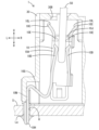
- FIG. 1 is a side cross-sectional view of a connector according to an embodiment.
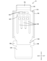
- FIG. 2 is a plan view of the terminal fitting as viewed from above.
- FIG. 3 is a cross-sectional view taken along line AA in FIG.
- FIG. 4 is a perspective view of the terminal fitting with a part of the box portion cut away.
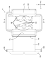
- FIG. 5 is a plan view of the connector as viewed from above.
- FIG. 6 is a side cross-sectional view showing a state in which a mating terminal is inserted into the terminal fitting.
- a housing A terminal metal fitting accommodated in the housing; Equipped with The terminal fitting of this connector has a box portion into which a mating terminal is inserted, a connection portion connected to a circuit board, and a spring portion extending from the connection portion and arranged non-contact with the housing to support the box portion so as to be displaceable.
- the spring portion is not in contact with the housing, so it is possible to maintain a stable connection between the terminal fitting and the mating terminal while absorbing misalignment of the mating terminal without being affected by the housing that is deformed due to changes in temperature and humidity.
- the box portion has a cylindrical shape with both ends open, The connector according to (1), wherein when the box portion is viewed from the opening direction, the spring portion and the connection portion are positioned outside the opening.
- the terminal fitting (2) has a spring portion positioned outside the opening. For example, when inspecting the unevenness inside the box using laser light, the spring portion and connection portion do not block the laser light, making the inspection easy.
- the housing has an insertion hole formed to face one of the openings of the box portion,
- the connector according to claim 2 wherein at least a portion of an inner surface of the insertion hole is located inside an outer surface of the box portion when viewed from the opening direction.
- the terminal fitting (3) makes it difficult for the mating terminal to hit the open end of the box portion when the mating terminal is inserted into the box portion.
- the terminal fitting (4) allows the excess length of the spring portion to be increased, making it easier to elastically deform and easier to maintain the function of supporting the box portion in a displaceable manner.
- the connector 1 can connect the terminal fittings 10 housed in the housing 30 to the mating terminals 50 of a mating connector (not shown).
- the connector 1 includes a pair of terminal fittings 10 and a housing 30.
- the connector 1 is attached to a circuit board S.
- the circuit board S is in the shape of a flat plate. Electronic components (not shown) are mounted on the upper and lower surfaces of the circuit board S. A pair of through holes H are formed penetrating the circuit board S in the plate thickness direction. A conductive portion La is provided on the lower surface of the circuit board S so as to surround the through holes H. A connection portion 10H of a terminal fitting 10 that is inserted into the through holes H and protrudes from the lower surface of the circuit board S is fixed to the conductive portion La by soldering.
- the terminal fittings 10 are formed by pressing a conductive metal plate or the like.
- the terminal fittings 10 are so-called female terminal fittings.
- the pair of terminal fittings 10 have the same shape and differ only in the position in which they are arranged. Therefore, the terminal fittings 10 will be described with reference to one of the terminal fittings 10.
- the terminal fittings 10 have a box portion 10A, a plurality of inclined portions 10C, a plurality of elastic contact portions 10D, a plurality of protrusions 10E, a spring portion 10G, and a connection portion 10H.
- the box portion 10A is in the shape of a rectangular tube, its axis is oriented in the vertical direction, and the upper and lower ends (i.e., both ends) are open (see FIG. 4).
- the upper end of the box portion 10A is an insertion opening 10J into which the mating terminal 50 is inserted (see FIGS. 3 and 4). That is, the box portion 10A has an insertion opening 10J into which the mating terminal 50 is inserted.
- the housing 30 has an insertion hole 30B formed to face one opening of the box portion 10A, and when the connector 1 is viewed from the opening direction, a part of the inner peripheral surface of the insertion hole 30B is located inside the outer peripheral surface of the box portion 10A.
Landscapes
- Coupling Device And Connection With Printed Circuit (AREA)
- Connector Housings Or Holding Contact Members (AREA)
Priority Applications (1)
| Application Number | Priority Date | Filing Date | Title |
|---|---|---|---|
| CN202480064247.1A CN121970215A (zh) | 2023-10-25 | 2024-10-10 | 连接器 |
Applications Claiming Priority (2)
| Application Number | Priority Date | Filing Date | Title |
|---|---|---|---|
| JP2023-182930 | 2023-10-25 | ||
| JP2023182930A JP2025072702A (ja) | 2023-10-25 | 2023-10-25 | コネクタ |
Publications (1)
| Publication Number | Publication Date |
|---|---|
| WO2025089089A1 true WO2025089089A1 (ja) | 2025-05-01 |
Family
ID=95515662
Family Applications (1)
| Application Number | Title | Priority Date | Filing Date |
|---|---|---|---|
| PCT/JP2024/036237 Pending WO2025089089A1 (ja) | 2023-10-25 | 2024-10-10 | コネクタ |
Country Status (3)
| Country | Link |
|---|---|
| JP (1) | JP2025072702A (cg-RX-API-DMAC7.html) |
| CN (1) | CN121970215A (cg-RX-API-DMAC7.html) |
| WO (1) | WO2025089089A1 (cg-RX-API-DMAC7.html) |
Cited By (2)
| Publication number | Priority date | Publication date | Assignee | Title |
|---|---|---|---|---|
| WO2026058594A1 (ja) * | 2024-09-16 | 2026-03-19 | 株式会社オートネットワーク技術研究所 | コネクタ |
| WO2026058593A1 (ja) * | 2024-09-16 | 2026-03-19 | 株式会社オートネットワーク技術研究所 | 端子金具 |
Families Citing this family (1)
| Publication number | Priority date | Publication date | Assignee | Title |
|---|---|---|---|---|
| JP2026087591A (ja) * | 2024-11-18 | 2026-05-28 | 株式会社オートネットワーク技術研究所 | コネクタ |
Citations (4)
| Publication number | Priority date | Publication date | Assignee | Title |
|---|---|---|---|---|
| JP2017135020A (ja) * | 2016-01-28 | 2017-08-03 | イリソ電子工業株式会社 | コネクタ |
| JP2018206624A (ja) * | 2017-06-06 | 2018-12-27 | イリソ電子工業株式会社 | 多接点コネクタ |
| JP2020202012A (ja) * | 2019-06-06 | 2020-12-17 | I−Pex株式会社 | 端子及びコネクタ |
| JP2022103927A (ja) * | 2020-12-28 | 2022-07-08 | ヒロセ電機株式会社 | 相手端子の挿入時の位置ずれを許容することができるコネクタ |
-
2023
- 2023-10-25 JP JP2023182930A patent/JP2025072702A/ja active Pending
-
2024
- 2024-10-10 WO PCT/JP2024/036237 patent/WO2025089089A1/ja active Pending
- 2024-10-10 CN CN202480064247.1A patent/CN121970215A/zh active Pending
Patent Citations (4)
| Publication number | Priority date | Publication date | Assignee | Title |
|---|---|---|---|---|
| JP2017135020A (ja) * | 2016-01-28 | 2017-08-03 | イリソ電子工業株式会社 | コネクタ |
| JP2018206624A (ja) * | 2017-06-06 | 2018-12-27 | イリソ電子工業株式会社 | 多接点コネクタ |
| JP2020202012A (ja) * | 2019-06-06 | 2020-12-17 | I−Pex株式会社 | 端子及びコネクタ |
| JP2022103927A (ja) * | 2020-12-28 | 2022-07-08 | ヒロセ電機株式会社 | 相手端子の挿入時の位置ずれを許容することができるコネクタ |
Cited By (2)
| Publication number | Priority date | Publication date | Assignee | Title |
|---|---|---|---|---|
| WO2026058594A1 (ja) * | 2024-09-16 | 2026-03-19 | 株式会社オートネットワーク技術研究所 | コネクタ |
| WO2026058593A1 (ja) * | 2024-09-16 | 2026-03-19 | 株式会社オートネットワーク技術研究所 | 端子金具 |
Also Published As
| Publication number | Publication date |
|---|---|
| CN121970215A (zh) | 2026-05-01 |
| JP2025072702A (ja) | 2025-05-12 |
Similar Documents
| Publication | Publication Date | Title |
|---|---|---|
| JP2025072702A (ja) | コネクタ | |
| US9478924B2 (en) | Electrical connector | |
| US4715819A (en) | Connector for printed board connection | |
| US7186126B2 (en) | Floating electrical connector | |
| US7381071B2 (en) | Floating electrical connector with twisted contacts | |
| US8272889B2 (en) | Connector | |
| US7713095B2 (en) | Contact | |
| EP3413398A1 (en) | Multi-contact connector | |
| JP2007220327A (ja) | フローティング型コネクタ | |
| JP2012142221A (ja) | コネクタ | |
| JP4514064B2 (ja) | 回路基板用電気コネクタ | |
| US10826211B2 (en) | Connector contact with dual contact beams derived from different contact strips | |
| JP2011014365A (ja) | 水平基板間接続コネクタ | |
| JP2019160455A (ja) | 中間電気コネクタ及び電気コネクタ組立体 | |
| JP5786515B2 (ja) | コネクタ及びこのコネクタの組み立て方法 | |
| JP4915759B2 (ja) | フレキシブル基板接続用コネクタ | |
| JP2006012625A (ja) | 基板対基板コネクタ | |
| JP2654498B2 (ja) | 電気コネクタ組立体および電気端子 | |
| JP2011048982A (ja) | フローティングコネクタ | |
| WO2025089093A1 (ja) | 端子金具 | |
| WO2025089092A1 (ja) | 端子金具 | |
| US6840814B2 (en) | Connector for printed circuit board | |
| KR102148179B1 (ko) | 커넥터 어셈블리 | |
| KR20220112665A (ko) | 기판 커넥터 | |
| JP2022040584A (ja) | コネクタ |
Legal Events
| Date | Code | Title | Description |
|---|---|---|---|
| 121 | Ep: the epo has been informed by wipo that ep was designated in this application |
Ref document number: 24875750 Country of ref document: EP Kind code of ref document: A1 |
|
| NENP | Non-entry into the national phase |
Ref country code: DE |