WO2025079734A1 - 磁気メモリ素子 - Google Patents
磁気メモリ素子 Download PDFInfo
- Publication number
- WO2025079734A1 WO2025079734A1 PCT/JP2024/036724 JP2024036724W WO2025079734A1 WO 2025079734 A1 WO2025079734 A1 WO 2025079734A1 JP 2024036724 W JP2024036724 W JP 2024036724W WO 2025079734 A1 WO2025079734 A1 WO 2025079734A1
- Authority
- WO
- WIPO (PCT)
- Prior art keywords
- layer
- memory element
- magnetic memory
- antiferromagnetic
- magnetic
- Prior art date
- Legal status (The legal status is an assumption and is not a legal conclusion. Google has not performed a legal analysis and makes no representation as to the accuracy of the status listed.)
- Pending
Links
Images






Classifications
-
- H—ELECTRICITY
- H10—SEMICONDUCTOR DEVICES; ELECTRIC SOLID-STATE DEVICES NOT OTHERWISE PROVIDED FOR
- H10B—ELECTRONIC MEMORY DEVICES
- H10B61/00—Magnetic memory devices, e.g. magnetoresistive RAM [MRAM] devices
-
- H—ELECTRICITY
- H10—SEMICONDUCTOR DEVICES; ELECTRIC SOLID-STATE DEVICES NOT OTHERWISE PROVIDED FOR
- H10N—ELECTRIC SOLID-STATE DEVICES NOT OTHERWISE PROVIDED FOR
- H10N50/00—Galvanomagnetic devices
- H10N50/10—Magnetoresistive devices
Definitions
- the present invention relates to a magnetic memory element.
- Patent document 1 discloses a technology for providing a magnetic memory element 1 that can operate at high speed with a small current.
- the magnetic memory element 1 includes a perpendicular magnetization layer whose magnetization direction is perpendicular to the film surface, a non-magnetic layer, a ferromagnetic layer having an easy axis of magnetization in the in-plane direction and whose magnetization direction is tilted at an angle of 15 degrees to 45 degrees from the direction perpendicular to the film surface, a memory layer in which the perpendicular magnetization layer and the ferromagnetic layer are stacked with the non-magnetic layer interposed therebetween and magnetically coupled to each other, a magnetization fixed layer whose magnetization direction is fixed in the direction perpendicular to the film surface, and a non-magnetic intermediate layer disposed between the memory layer and the magnetization fixed layer, and is configured so that information is recorded by passing a current in the stacking direction of each layer.
- a magnetic memory element comprising a fixed layer and a storage layer, the fixed layer being configured to have spontaneous magnetization along the stacking direction, the magnetization direction of the fixed layer being configured to be fixed regardless of data written to the magnetic memory element, the storage layer being stacked on the fixed layer along the stacking direction via an electrically insulating barrier layer, the storage layer being configured to have a first ferromagnetic layer and an antiferromagnetic layer, the first ferromagnetic layer being configured to have spontaneous magnetization along the stacking direction, the magnetization direction of the first ferromagnetic layer being configured to be reversible according to data written to the magnetic memory element using a tunnel current through the fixed layer and the storage layer, the antiferromagnetic layer including an antiferromagnetic material that exhibits an anomalous Hall effect by forming a non-collinear or non-coplanar magnetic order in the a-b plane defined by the a-axis and the b-axis perpendicular to the c-
- This configuration makes it possible to provide a new magnetic memory element that can write data more efficiently.
- FIG. 1 is a diagram showing a configuration example of a magnetic memory element.
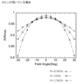
- 13 is a measurement example of the tilt angle ⁇ 1 of the magnetization of the storage layer 3 by rotational hysteresis measurement in the case where the magnetic moment M2 of the first ferromagnetic layer 5 is tilted with respect to the stacking direction D1.
- 13 is a measurement example of the tilt angle ⁇ 1 of the magnetization of the storage layer 3 by rotational hysteresis measurement in a case where the magnetic moment M2 of the first ferromagnetic layer 5 is not tilted with respect to the stacking direction D1.
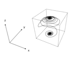
- 1 shows the reversal history of the magnetization M2 when calculations are performed using only the first ferromagnetic layer 5 having a diameter of 50 nm.
- FIG. 1 shows the reversal history of the magnetization M2 when the first ferromagnetic layer 5 is magnetically coupled to the antiferromagnetic layer 6.
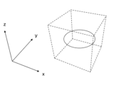
- 2 is a diagram showing a history of changes in the direction of the magnetic moment of an antiferromagnetic layer 6.
- FIG. FIG. 13 is a diagram showing calculation results regarding the relationship between the pulse width (PW) and the reversal current Ic.
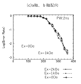
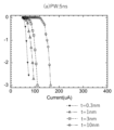
- FIG. 13 is a diagram showing the change in error rate according to the current when the antiferromagnetic material in the antiferromagnetic layer 6 is oriented along the c-axis.
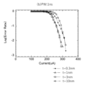
- FIG. 13 is a diagram showing the change in error rate according to the current when the antiferromagnetic material in the antiferromagnetic layer 6 is randomly oriented polycrystalline.
- FIG. 13 is a diagram showing the change in error rate according to the current when the antiferromagnetic material in the antiferromagnetic layer 6 is oriented along the a-axis or the b-axis.
- the calculation results of the error rate when the pulse width is 5 ns are shown.
- the calculation results of the error rate when the pulse width is 1 ns are shown.
- 2 is a diagram showing a layer structure of a magnetic memory element 1 according to a comparative example.
- FIG. 1 is a diagram showing a layer structure of a magnetic memory element 1 according to a first embodiment
- 11 is a diagram showing a layer structure of a magnetic memory element 1 according to a second embodiment.
- FIG. FIG. 11 is a diagram showing a layer structure of a magnetic memory element 1 according to a third embodiment.
- the program for realizing the software appearing in one embodiment may be provided as a non-transitory computer-readable recording medium, or may be provided so that it can be downloaded from an external server, or may be provided so that the program is started on an external computer and its functions are realized on a client terminal (so-called cloud computing).
- an input and an output according to the input can be realized.
- the form of the information referenced in such information processing (hereinafter referred to as reference information) is not limited.
- the reference information may be, for example, rule-based information such as a database, a lookup table, or a predetermined function (including a decision formula such as a regression formula constructed by a statistical method), or it may be a trained model that has previously learned the correlation between the input and the output, or it may be a large-scale language model that can output a desired result by inputting a prompt.
- a "part” may include, for example, a combination of hardware resources implemented by a circuit in the broad sense and software information processing that can be specifically realized by these hardware resources.
- various information is handled, and this information is represented, for example, by physical values of signal values representing voltage and current, high and low signal values as a binary bit collection consisting of 0 or 1, or quantum superposition (so-called quantum bits), and communication and calculations can be performed on a circuit in the broad sense.
- a circuit in the broad sense is a circuit realized by at least an appropriate combination of a circuit, circuits, a processor, and a memory.
- the processor may be a general-purpose processor or a dedicated circuit. That is, it includes application specific integrated circuits (ASICs), programmable logic devices (e.g., simple programmable logic devices (SPLDs), complex programmable logic devices (CPLDs), and field programmable gate arrays (FPGAs)).
- ASICs application specific integrated circuits
- SPLDs simple programmable logic devices
- CPLDs complex programmable logic devices
- FPGAs field programmable gate arrays
- a magnetic memory element 1 is a diagram showing a configuration example of a magnetic memory element.
- a magnetic memory element 1 includes a fixed layer 2, a tunnel barrier layer 3, and a memory layer 4. These layers 11 to 13 are stacked along a stacking direction D1, and a pair of electrodes (not shown) is provided on both ends of the stacked structure.
- the magnetic memory element 1 of this embodiment is a so-called Spin Transfer Torque (STT)-RAM.
- the fixed layer 2 is configured to have spontaneous magnetization M1 along the stacking direction D1.
- the magnetization direction of the fixed layer 2 is configured to be fixed regardless of the data written to the magnetic memory element 1.
- the fixed layer 2 is, for example, a perpendicular magnetization layer that forms a pinned layer, and the magnetization direction of the spontaneous magnetization M1 is approximately the same as the stacking direction D1.
- the tunnel barrier layer 3 is a non-magnetic insulating layer provided to realize giant magnetoresistance (TMR).
- the tunnel barrier layer 3 is not particularly limited as long as it functions as an insulating layer, and may be made of, for example, MgO, AlO x , TiO x , or the like.
- the memory layer 4 is stacked on the fixed layer 2 via the electrically insulating tunnel barrier layer 3 along the stacking direction D1. This allows a tunnel current to flow between the fixed layer 2 and the memory layer 4 via the tunnel barrier layer 3.
- the memory layer 4 includes a first ferromagnetic layer 5 and an antiferromagnetic layer 6.
- the angle is preferably less than 35 degrees, more preferably less than 25 degrees, more preferably less than 15 degrees, and even more preferably less than 5 degrees. It is particularly preferable that the antiferromagnetic material is a single crystal whose c-axis and the stacking direction D1 are approximately aligned.
- the c-axis orientation can be evaluated based on the three-dimensional orientation distribution obtained by single crystal structure analysis methods such as transmission electron diffraction and X-ray diffraction.
- the crystal orientation to the c-axis can be evaluated by the half-width of a specific reflection spot (for example, the (002) reflection spot in Mn3Sn). Therefore, when an antiferromagnetic material has a crystal orientation in which the c-axis extends in the stacking direction D1, it can mean that the half-width of the specific reflection spot is 30 degrees or less, preferably 10 degrees or less.
- An antiferromagnetic layer 6 with a half-width of 10 degrees or less is a highly oriented film
- an antiferromagnetic layer 6 with a half-width of more than 10 degrees and less than 30 degrees is a medium oriented film
- an antiferromagnetic layer 6 with a half-width of more than 30 degrees is a low oriented film, which are in a state of having a relatively random orientation.
- Such an antiferromagnetic material that exhibits the anomalous Hall effect by forming a non-collinear or non-coplanar magnetic order can be configured to form a spin frustration system such as a triangular lattice or a kagome lattice in the ab plane.
- the antiferromagnetic material is a hexagonal system having a six-fold rotation axis in the c-axis direction, and is preferably in the space group P6 3 /mmc.
- Such an antiferromagnetic material can be composed of one or more substances selected from the group consisting of Mn 3 Sn, Mn 3 Pt, Mn 3 Ge, Mn 3 Ga, and Mn 3 Ir.
- the magnetic moment of each atom is aligned in the ab plane, so it is preferable to form the c-axis of the crystal to face the stacking direction D1.
- the magnetic moment may be oriented in a manner not aligned in the c-axis direction or randomly oriented.
- Such a triangular magnetization structure can be realized by an alloy of Mn and at least one of Ge, Ga, and Sn, but the type of alloy is not limited to this. Also, even without using the above-mentioned alloys, it is possible to create a triangular arrangement of magnetic moments similar to that of a hexagonal structure by creating a periodic layered structure of magnetic elements and non-magnetic elements.
- the sign of the anomalous Hall coefficient of the antiferromagnetic material is not reversed by writing to the magnetic memory element 1.
- the direction of the internal magnetic field is less likely to change significantly, and the behavior of the spin of the first ferromagnetic layer 5 included in the memory layer 4 can be stabilized. Therefore, the operation of the magnetic memory element can be more easily stabilized.
- the sign of the anomalous Hall coefficient in other words, the direction of the electromotive force based on the anomalous Hall effect for a certain current direction, may be caused by the spin chirality (e.g., vector spin chirality, scalar spin chirality, etc.) taking a finite value due to a non-collinear or non-coplanar magnetic order. Therefore, the fact that the sign of the anomalous Hall coefficient does not reverse may correspond to the fact that the relative orientation of adjacent spins (especially electron spins) that define the spin chirality does not reverse.
- the spin chirality e.g., vector spin chirality, scalar spin chirality, etc.
- the magnetization of each magnetic atom is arranged in a triangle with an angle of about 120 degrees, so that there is almost no effective magnetization.
- a Weyl magnet such as Mn 3 Sn having a DO 19 type crystal structure has a large internal magnetic field derived from its band structure, and shows a large Hall effect and magnetic Kerr effect disproportionate to the magnetization amount.
- These antiferromagnetic materials are, for example, "non-collinear antiferromagnetic materials".
- the magnetization plane of the atoms arranged in a triangle has a characteristic that the direction of magnetization is easy to change, but difficult to change in the perpendicular direction.
- the thickness of the antiferromagnetic layer 6 is not particularly limited, but is preferably 20 nm or less, and more preferably 10 nm or less.
- the magnetic memory element 1 may include an intermediate layer 7 between the first ferromagnetic layer 5 and the antiferromagnetic layer 6.
- the intermediate layer 7 may be composed of one or more nonmagnetic elements or compounds such as B, C, N, O, F, Mg, Al, Si, P, Ti, V, Cr, Cu, Zn, Ga, Ge, Y, Zr, Nb, Mo, Ru, Rh, Pd, Ag, Cd, In, Sn, Sb, Hf, Ta, W, Re, Os, IrPt, and Au.
- the intermediate layer 7 may include a layer composed of an antiferromagnetic material such as PtMn or IrMn whose magnetic moments are arranged antiparallel.
- the intermediate layer 7 may also contain magnetic elements such as Fe, Co, Ni, etc., to the extent that the perpendicular magnetization of the first ferromagnetic layer 5 is not significantly degraded. With this configuration, a more stable interface can be formed between the first ferromagnetic layer 5 and the antiferromagnetic layer 6. From another perspective, the generation of a magnetic degradation layer at the interface between the first ferromagnetic layer 5 and the antiferromagnetic layer 6 can be suppressed.
- the magnetic memory element 1 may have elements such as B, C, Fe, Co, W, Mo, Ir, and Rh inserted between the tunnel barrier layer 3 and the memory layer 4 (specifically, the first ferromagnetic layer 5). This can improve the magnetoresistance (MR) effect and heat resistance.
- elements such as B, C, Fe, Co, W, Mo, Ir, and Rh inserted between the tunnel barrier layer 3 and the memory layer 4 (specifically, the first ferromagnetic layer 5). This can improve the magnetoresistance (MR) effect and heat resistance.
- MR magnetoresistance
- the antiferromagnetic layer 6 generates a virtual internal magnetic field along the c-axis direction due to the antiferromagnetic magnetic order formed in the ab plane.
- the internal magnetic field affects the motion of the spins (e.g., precession around the stacking direction D1) that are responsible for the spontaneous magnetization of the first ferromagnetic layer through the interaction between the first ferromagnetic layer and the antiferromagnetic layer 6.
- the antiferromagnetic body has a domain whose c-axis is along the stacking direction D1, thereby generating an internal magnetic field along the stacking direction D1.
- the internal magnetic field induces precession around the stacking direction D1 in the spins in the first ferromagnetic layer in a state tilted from the stacking direction D1. This shortens the time required to induce precession when the spins in the first ferromagnetic layer are reversed, and therefore the spin reversal speed can be increased compared to the conventional technology. Therefore, it is possible to provide a magnetic memory element that allows data to be written at a higher speed.
- the tilt angle ⁇ 1 can be estimated by measuring the rotational hysteresis loss of the magnetic memory element 1.
- FIG. 2 shows an example of measuring the tilt angle ⁇ 1 of the magnetization of the memory layer 3 by rotational hysteresis measurement when the magnetic moment M2 of the first ferromagnetic layer 5 is tilted with respect to the stacking direction D1.
- FIG. 3 shows an example of measuring the tilt angle ⁇ 1 of the magnetization of the memory layer 3 by rotational hysteresis measurement when the magnetic moment M2 of the first ferromagnetic layer 5 is not tilted with respect to the stacking direction D1.
- the magnetization tilt angle ⁇ 1 can be obtained by measuring the rate of change in resistance in a rotating magnetic field.
- the magnetization tilt angle ⁇ 1 of the memory layer first ferromagnetic layer 5
- no resistance change occurs.
- the resistance curves of multiple applied magnetic fields will cross at the tilt angle ⁇ 1.
- the resistance curves will overlap at the angle of 0 degrees, but no crossing will occur. In this way, the magnetization tilt angle ⁇ 1 can be obtained. In this way, the technology disclosed herein can realize a non-volatile memory that can operate at high speed with a small current.
- the inventor of the present application first performed a simulation calculation of spin torque magnetization reversal by the Landau-Lifshitz-Gilbert (LLG) equation.
- the calculation was performed with the following ferromagnetic layer: magnetization amount 1000 emu/cm 3 , thickness 1.5 nm, perpendicular magnetic anisotropy 5 kOe, damping constant 0.01, and spin injection efficiency 50%.
- the antiferromagnetic layer was assumed to have no effective magnetization, the magnetic moments of antiferromagnetic atoms were arranged in a triangle, and no in-plane anisotropy was assumed, the in-plane binding magnetic field was 100 Tesla, and the damping constant was 0.01.
- Figure 4 shows the reversal history of magnetization M2 when calculations were performed using only the first ferromagnetic layer 5 with a diameter of 50 nm.
- the reversal of magnetization M2 was from positive to negative along the z-axis, and the applied pulse width was 5 ns.
- Figure 5 shows the reversal history of magnetization M2 when the antiferromagnetic layer 6 is magnetically coupled to the first ferromagnetic layer 5.
- the characteristics of the first ferromagnetic layer 5 are the same as those used in Figure 5.
- the magnetic coupling strength between the first ferromagnetic layer 5 and the antiferromagnetic layer 6 was set so that the effective magnetic field to the first ferromagnetic layer 5 was equivalent to 1 kOe.
- the calculation was performed with the thickness of the antiferromagnetic layer 6 being 3 nm.
- Figure 6 shows the history of changes in the orientation of the magnetic moment of the antiferromagnetic layer 6.
- the magnetic moment of the antiferromagnetic layer 6 rotates while remaining almost entirely within the ab plane, resulting in a ring-shaped magnetization trajectory.
- This result also suggests that each magnetic moment (in other words, spin) rotates within the ab plane while maintaining a 120-degree structure, suggesting that the sign of the spin chirality, such as the vector spin chirality, is not inverted in the antiferromagnetic layer 6.
- Figure 7 shows the calculation results regarding the relationship between the pulse width (PW) and the reversal current Ic.
- PW pulse width
- Figure 7 shows the calculation results regarding the relationship between the pulse width (PW) and the reversal current Ic.
- calculations were performed for two cases: (a) when the memory layer 4 is composed of only the first ferromagnetic layer 5, and (b) when the memory layer 4 is composed of the first ferromagnetic layer 5 and the antiferromagnetic layer 6.
- the reversal current Ic when the ferromagnetic layer 131 and the antiferromagnetic layer 6 are stacked is lower than when the first ferromagnetic layer 5 is a single layer. Note that the above calculation is for a case where the triangular magnetic moment is arranged in the film plane.
- the antiferromagnetic material constituting the antiferromagnetic layer 6 is a hexagonal crystal with the c-axis perpendicular to the triangular magnetic moment and the a-axis and b-axis in-plane
- the antiferromagnetic material in the antiferromagnetic layer 6 is (a) oriented along the c-axis, (b) randomly oriented polycrystal, and (c) oriented along the a-axis or b-axis
- FIG. 8 is a diagram showing the change in error rate corresponding to the current when the antiferromagnetic material in the antiferromagnetic layer 6 is oriented along the c-axis.
- Figure 9 is a diagram showing the change in error rate corresponding to the current when the antiferromagnetic material in the antiferromagnetic layer 6 is randomly oriented polycrystal.
- FIG. 10 shows the change in error rate according to the current when the antiferromagnetic material in the antiferromagnetic layer 6 is oriented along the a-axis or the b-axis. In FIGS. 8 to 10, the reversal current is shown on the horizontal axis, and the error rate is shown on a logarithmic scale on the vertical axis.
- FIG. 13 is a diagram showing the layer structure of a magnetic memory element 1 according to a comparative example.
- the magnetic memory element 1 according to the comparative example is composed of an underlayer 9, a pinned layer 10, an antiferromagnetic magnetic coupling layer 11, a reference layer 12, a tunnel barrier layer 13, a ferromagnetic layer 14 constituting a memory layer, and a cap layer 15.
- the underlayer 9 was obtained by stacking a 5 nm thick Ru layer on a 2 nm thick Ta layer.
- the pinned layer 10 which corresponds to the fixed layer, was obtained by stacking a composite layer of Co and Pt with a thickness of about 4 nm on a Ru layer.
- the composite layer was constructed so that Co layers with a thickness of about 0.8 nm and Pt layers with a thickness of about 0.6 nm were stacked alternately.
- the cap layer 15 was formed by sequentially stacking a 1 nm thick Mo layer, a 0.5 nm thick MgO layer, a 1 nm thick Ru layer, and a 5 nm thick Ta layer on the ferromagnetic layer 14.
- the magnetic memory element 1 according to the comparative example was formed into a circle with a diameter of 70 nm, and electrodes were connected to both ends to obtain a measurement sample according to the first embodiment.
- the antiferromagnetic magnetic coupling layer 26 in Example 2 was obtained by sequentially stacking an Ir layer having a thickness of 0.6 nm and an Mo layer having a thickness of 0.3 nm on the pinned layer 25.
- the ferromagnetic layer 29 in Example 2 was obtained by sequentially stacking a 0.3 nm thick carbon (C) layer and a 1.3 nm thick CoFe layer on the tunnel barrier layer 28.
- the antiferromagnetic layers 30 and 31 in accordance with the second embodiment were obtained by laminating a 2 nm-thick MnIr layer 30 and a 3 nm-thick Mn 3 Sn layer 31 in this order on the ferromagnetic layer 29 .
- the cap layer 32 in Example 2 was obtained by sequentially stacking a 0.5 nm thick MgO layer and a 5 nm thick Ru layer on the Mn3Sn layer 31. Electrodes (not shown) are connected to the layers at both ends of the magnetic memory element 1 in Example 2.
- the magnetic memory element 1 according to Example 2 was formed into a circle with a diameter of 70 nm, and electrodes were connected to both ends to obtain a measurement sample according to Example 2.
- Example 3 is a diagram showing a layer structure of a magnetic memory element 1 according to Example 3.
- the magnetic memory element 1 according to Example 3 is composed of an underlayer 33, a first ferromagnetic layer 34 constituting a memory layer, an antiferromagnetic layer 35 constituting the memory layer, a first antiferromagnetic magnetic coupling layer 36 constituting the memory layer, a second ferromagnetic layer 37 constituting the memory layer, a tunnel barrier layer 38, a reference layer 39, a second antiferromagnetic magnetic coupling layer 40 for coupling the magnetizations of the pinned layer 41 and the reference layer 39 in antiparallel, the pinned layer 41, and a cap layer 42.
- the first ferromagnetic layer 34 in Example 3 was obtained by stacking a 0.6 nm thick Co layer on the MgO layer of the underlayer 33.
- the second ferromagnetic layer 37 in Example 3 was obtained by stacking a 1 nm thick CoFeB layer on the W layer of the first antiferromagnetic magnetic coupling layer 36.
- the reference layer 39 in Example 3 was obtained by stacking a 1 nm thick CoFeB layer, a 0.3 nm thick Ta layer, and a 0.5 nm thick Co layer on the second ferromagnetic layer 37.
- the cap layer 42 was obtained by stacking a 5 nm thick Ru layer on the pinned layer 41.
- Examples 1 to 3 had the same coercive force as the Comparative Example, but showed a reduction in reversal current of about 30% at a pulse width of 10 ns, and a reversal voltage that was nearly halved at a pulse width of 2 ns. All of Examples 1 to 3 had an antiferromagnetic layer, whereas only the Comparative Example did not have such an antiferromagnetic layer. This suggests that the fact that the memory layer includes a ferromagnetic layer and an antiferromagnetic layer contributes to the reduction in reversal voltage in Examples 1 to 3 compared to the Comparative Example. These results suggest that the antiferromagnetic layer 6 as described above strengthens the initial tilt angle ⁇ 1 of the magnetic moment M2 of the first ferromagnetic layer 5.
- the above evaluation results suggest that in a magnetic memory element 1 in which a fixed layer 2, which serves as the basis for information, and a memory layer 4 in which information is recorded, are stacked via a tunnel barrier layer 3, the fixed layer 2 is a perpendicular magnetization film, and the memory layer 4 is composed of a laminated film of a first ferromagnetic layer 5 having a perpendicular easy axis of magnetization and an antiferromagnetic material in which the atomic magnetic moments are arranged at an angle of approximately 120 degrees, so that the magnetization of the first ferromagnetic layer 5 can form a cone-shaped easy magnetization direction inclined at a certain angle from the easy axis of magnetization, making it possible to record with a small current and a short recording time.
- the stacked structure included in the magnetic memory element 1 can be formed by any method, such as molecular beam epitaxy, and is not limited to sputtering.
- the magnetic memory element 1 is not limited to being connected to electrodes, etc. In other words, as long as the memory layer 4 including the first ferromagnetic layer 5 and the antiferromagnetic layer 6 is connected to the fixed layer 2 via the tunnel barrier layer 3, the structure and distribution mode are arbitrary.
- the direction of the internal magnetic field is less likely to change significantly, which stabilizes the behavior of the spins in the first ferromagnetic layer contained in the memory layer. This makes it easier to stabilize the operation of the magnetic memory element.
- a magnetic memory element according to (1) or (2) above, wherein the antiferromagnetic body is configured to have a crystal orientation such that the c-axis extends in the stacking direction.
- a magnetic memory element according to any one of (1) to (3) above, wherein the antiferromagnetic body is composed of domains whose c-axes are aligned with the stacking direction.
- This configuration makes it possible to further strengthen the internal magnetic field that contributes to the first ferromagnetic layer, thereby providing a magnetic memory element that allows data to be written at even higher speeds.
- a magnetic memory element according to any one of (1) to (4) above, wherein the antiferromagnetic material is a hexagonal crystal system having a six-fold rotation axis along the c-axis.
- the antiferromagnetic body is composed of one or more substances selected from the group consisting of Mn 3 Sn, Mn 3 Pt, Mn 3 Ge, Mn 3 Ga, and Mn 3 Ir.
- a magnetic memory element according to any one of (1) to (6) above, wherein the first ferromagnetic layer contains at least Co as a magnetic element.
- a magnetic memory element according to any one of (1) to (7) above, wherein the memory layer further includes a second ferromagnetic layer, and the second ferromagnetic layer is stacked on the first ferromagnetic layer via the antiferromagnetic layer.
- a magnetic memory element that records information by the direction of magnetization comprising: a magnetization fixed layer in which magnetization is fixed in one direction; and a memory layer in which the direction of magnetization changes in response to information, the memory layer and the fixed layer face each other via a tunnel barrier layer, and recording is performed by passing a current between the fixed layer and the memory layer via the tunnel barrier layer, the fixed layer being a perpendicular magnetization film, and the memory layer being a laminated film of a perpendicular magnetization ferromagnetic layer having a perpendicular easy axis of magnetization and an antiferromagnetic layer made of a non-collinear antiferromagnetic material.
- (Item 14) A memory device having the magnetic memory element of any one of items 1 to 13. It should be noted that the problems that can be solved by the above-described magnetic memory element 1 are not limited to those described above. For example, the problems may be solved in the following manner.
- DRAM which operates at high speed and has a high density, is widely used as random access memory (RAM).
- RAM random access memory
- DRAM is a volatile memory in which the information is lost when the power is turned off, so non-volatile memory in which the information is not lost is desired.
- Magnetic random access memory which records information by the magnetization of magnetic materials, has attracted attention as a candidate for non-volatile memory, and its development is underway.
- STT-MRAM spin torque-type MRAM
- the spin injection efficiency depends on the angle between the magnetizations of the fixed layer and storage layer, and is zero when the angle is completely parallel or anti-parallel.
- the interface magnetic anisotropy generated at the interface between magnetic materials such as CoFeB, which are currently mainly used as memory layers, and oxides such as MgO has a predominant magnetic anisotropy in the direction perpendicular to the film surface, making it excellent as a perpendicular magnetic memory layer and providing stable retention characteristics.
- magnetic materials such as CoFeB, which are currently mainly used as memory layers
- oxides such as MgO
- This technology was developed based on this recognition. In other words, its purpose is to realize a magnetic memory element that can operate at high speed with low current even in a miniature element.
- the researchers were able to construct the memory layer that constitutes the magnetic memory element from a laminated film of a perpendicular magnetization layer with perpendicular magnetization and a triangular magnetic antiferromagnet in which the magnetic atoms are arranged at 120 degrees, thereby tilting the magnetization of the perpendicular magnetization layer in-plane and realizing a state in which the angle between the magnetization of the fixed layer and memory layer is always acted on by the spin torque with a certain degree of efficiency or higher.
- This makes it possible, for example, to shorten the reversal time and reduce the variation in reversal time.
Landscapes
- Hall/Mr Elements (AREA)
- Mram Or Spin Memory Techniques (AREA)
Priority Applications (1)
| Application Number | Priority Date | Filing Date | Title |
|---|---|---|---|
| JP2025522992A JP7708488B1 (ja) | 2023-10-13 | 2024-10-15 | 磁気メモリ素子 |
Applications Claiming Priority (2)
| Application Number | Priority Date | Filing Date | Title |
|---|---|---|---|
| JP2023177351 | 2023-10-13 | ||
| JP2023-177351 | 2023-10-13 |
Publications (1)
| Publication Number | Publication Date |
|---|---|
| WO2025079734A1 true WO2025079734A1 (ja) | 2025-04-17 |
Family
ID=95395867
Family Applications (1)
| Application Number | Title | Priority Date | Filing Date |
|---|---|---|---|
| PCT/JP2024/036724 Pending WO2025079734A1 (ja) | 2023-10-13 | 2024-10-15 | 磁気メモリ素子 |
Country Status (2)
| Country | Link |
|---|---|
| JP (1) | JP7708488B1 (https=) |
| WO (1) | WO2025079734A1 (https=) |
Citations (2)
| Publication number | Priority date | Publication date | Assignee | Title |
|---|---|---|---|---|
| WO2017018391A1 (ja) * | 2015-07-24 | 2017-02-02 | 国立大学法人東京大学 | メモリ素子 |
| JP2022166395A (ja) * | 2021-04-21 | 2022-11-02 | 国立大学法人東北大学 | 電子デバイス、その製造方法及びその使用方法 |
Family Cites Families (3)
| Publication number | Priority date | Publication date | Assignee | Title |
|---|---|---|---|---|
| JP2009081215A (ja) * | 2007-09-25 | 2009-04-16 | Toshiba Corp | 磁気抵抗効果素子およびそれを用いた磁気ランダムアクセスメモリ |
| WO2020166722A1 (ja) * | 2019-02-15 | 2020-08-20 | 国立大学法人東京大学 | スピントロニクス素子及び磁気メモリ装置 |
| US20240194235A1 (en) * | 2021-04-12 | 2024-06-13 | The University Of Tokyo | Magnetic memory element |
-
2024
- 2024-10-15 WO PCT/JP2024/036724 patent/WO2025079734A1/ja active Pending
- 2024-10-15 JP JP2025522992A patent/JP7708488B1/ja active Active
Patent Citations (2)
| Publication number | Priority date | Publication date | Assignee | Title |
|---|---|---|---|---|
| WO2017018391A1 (ja) * | 2015-07-24 | 2017-02-02 | 国立大学法人東京大学 | メモリ素子 |
| JP2022166395A (ja) * | 2021-04-21 | 2022-11-02 | 国立大学法人東北大学 | 電子デバイス、その製造方法及びその使用方法 |
Also Published As
| Publication number | Publication date |
|---|---|
| JP7708488B1 (ja) | 2025-07-15 |
| JPWO2025079734A1 (https=) | 2025-04-17 |
Similar Documents
| Publication | Publication Date | Title |
|---|---|---|
| CN103069564B (zh) | 磁阻效应元件以及磁性随机存取存储器 | |
| TWI530945B (zh) | Memory elements and memory devices | |
| US10937955B2 (en) | Memory element and memory device | |
| US8742518B2 (en) | Magnetic tunnel junction with free layer having exchange coupled magnetic elements | |
| JP6244617B2 (ja) | 記憶素子、記憶装置、磁気ヘッド | |
| US9847161B2 (en) | Multilayer magnetic storage element and storage device | |
| CN102610270B (zh) | 存储元件和存储器装置 | |
| TWI487155B (zh) | Memory elements and memory devices | |
| JP5987613B2 (ja) | 記憶素子、記憶装置、磁気ヘッド | |
| CN108738371B (zh) | 磁化反转元件、磁阻效应元件和存储设备 | |
| JP7352930B2 (ja) | 磁気素子、磁気メモリチップ、磁気記憶装置及び磁気素子の書き込み方法 | |
| CN102769100A (zh) | 存储元件和存储装置 | |
| JP2013033881A (ja) | 記憶素子及び記憶装置 | |
| JP6567272B2 (ja) | 磁性多層スタック | |
| WO2013080436A1 (ja) | 記憶素子、記憶装置 | |
| JP2013115399A (ja) | 記憶素子、記憶装置 | |
| CN102629489A (zh) | 存储元件和存储器装置 | |
| TW201222546A (en) | Memory element and memory device | |
| JP7708488B1 (ja) | 磁気メモリ素子 | |
| EP4676184A1 (en) | Memory element | |
| WO2013080437A1 (ja) | 記憶素子、記憶装置 |
Legal Events
| Date | Code | Title | Description |
|---|---|---|---|
| ENP | Entry into the national phase |
Ref document number: 2025522992 Country of ref document: JP Kind code of ref document: A |
|
| WWE | Wipo information: entry into national phase |
Ref document number: 2025522992 Country of ref document: JP |
|
| 121 | Ep: the epo has been informed by wipo that ep was designated in this application |
Ref document number: 24877328 Country of ref document: EP Kind code of ref document: A1 |