WO2025069764A1 - アンテナモジュールおよびそれを搭載した通信装置 - Google Patents
アンテナモジュールおよびそれを搭載した通信装置 Download PDFInfo
- Publication number
- WO2025069764A1 WO2025069764A1 PCT/JP2024/029055 JP2024029055W WO2025069764A1 WO 2025069764 A1 WO2025069764 A1 WO 2025069764A1 JP 2024029055 W JP2024029055 W JP 2024029055W WO 2025069764 A1 WO2025069764 A1 WO 2025069764A1
- Authority
- WO
- WIPO (PCT)
- Prior art keywords
- radiating element
- electrode
- antenna module
- dielectric substrate
- viewed
- Prior art date
- Legal status (The legal status is an assumption and is not a legal conclusion. Google has not performed a legal analysis and makes no representation as to the accuracy of the status listed.)
- Pending
Links
Images




Classifications
-
- H—ELECTRICITY
- H01—ELECTRIC ELEMENTS
- H01Q—ANTENNAS, i.e. RADIO AERIALS
- H01Q13/00—Waveguide horns or mouths; Slot antennas; Leaky-waveguide antennas; Equivalent structures causing radiation along the transmission path of a guided wave
- H01Q13/08—Radiating ends of two-conductor microwave transmission lines, e.g. of coaxial lines, of microstrip lines
-
- H—ELECTRICITY
- H01—ELECTRIC ELEMENTS
- H01Q—ANTENNAS, i.e. RADIO AERIALS
- H01Q15/00—Devices for reflection, refraction, diffraction or polarisation of waves radiated from an antenna, e.g. quasi-optical devices
- H01Q15/02—Refracting or diffracting devices, e.g. lens, prism
Definitions
- This disclosure relates to an antenna module and a communication device equipped with the same, and more specifically to technology for improving the directionality of an antenna that supports high-frequency signals in the sub-terahertz frequency band.
- Patent Document 1 discloses a configuration for supplying a high-frequency signal to a patch antenna through a stripline and a via.
- sub-terahertz frequency band which is greater than 100 GHz.
- the use of sub-terahertz frequency bands makes it possible to widen the spectral bandwidth, enabling high-capacity, high-speed communications of, for example, 100 Gbps or more.
- the influence of surface waves generated on the surface of the dielectric substrate on which the radiating element is placed tends to be large.
- the feed point is located at a position offset from the center of the element, which creates asymmetry in the electromagnetic field generated by the radiating element.
- the present disclosure has been made to solve these problems, and its purpose is to improve the directionality of antenna modules compatible with the sub-terahertz frequency band.
- the antenna module includes a dielectric substrate, a flat-plate-shaped first radiating element, a ground electrode, a first power supply wiring, and a flat-plate-shaped first electrode.
- the dielectric substrate has a first main surface and a second main surface that face each other.
- the first radiating element is disposed on the dielectric substrate.
- the ground electrode is disposed on the dielectric substrate closer to the second main surface than the first radiating element and facing the first radiating element.
- the first power supply wiring transmits a high-frequency signal to a first power supply point of the first radiating element.
- the first electrode is connected to the first power supply wiring and disposed between the first radiating element and the ground electrode.
- the first power supply point is disposed at a position offset from the center of the first radiating element in the first direction. When viewed in a plan view from the normal direction of the dielectric substrate, the first electrode protrudes from the first radiating element in the first direction.
- a plate electrode (first electrode) extending in the offset direction (first direction) of the power supply point is connected to a power supply wiring that transmits a high-frequency signal to the radiating element, and the plate electrode protrudes from the radiating element in the first direction.
- some of the electric field lines spreading from the radiating element in the first direction reach the ground electrode via the plate electrode. Therefore, the electric field lines spreading from the radiating element in the first direction are coupled to the ground electrode at a position closer to the radiating element than in the absence of the plate electrode. This suppresses the spread of the electric field lines from the radiating element in the first direction, thereby reducing the inclination of the beam in the first direction. Therefore, the directivity of the antenna module can be improved.
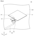
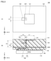
- FIG. 1 is an overall configuration diagram of a communication device to which an antenna module according to a first embodiment is applied; 1 is a perspective view showing an internal structure of an antenna module according to a first embodiment; 3A and 3B are a plan view and a side see-through view of the antenna module of FIG. 2 .
- 5A to 5C are diagrams illustrating an example of the electromagnetic field distribution and antenna gain of the antenna modules of the first embodiment and the comparative example.
- 13A and 13B are diagrams for explaining antenna gain when the width of the auxiliary electrode is changed.
- FIG. 11 is a side see-through view of an antenna module according to a second embodiment.
- FIG. 11 is a side see-through view of an antenna module according to a third embodiment.
- FIG. 13 is a perspective view of an antenna module according to a fourth embodiment.
- FIG. 13 is a perspective view of an antenna module according to a fifth embodiment.
- FIG. 13 is a plan view of an antenna module according to a sixth embodiment.
- FIG. 11 is a plan view of an antenna module according to a first modified example.
- FIG. 11 is a plan view of an antenna module according to a second modified example.
- FIG. 13 is a plan view of an antenna module according to a seventh embodiment.
- FIG. 13 is a side see-through view of an antenna module according to an eighth embodiment.
- FIG. 13 is a perspective view of an antenna module according to a ninth embodiment.
- 13 is a side see-through view of an antenna module according to a tenth embodiment.
- FIG. FIG. 23 is a side see-through view of an antenna module according to an eleventh embodiment.
- FIG. 23 is a side see-through view of an antenna module according to a twelfth embodiment.
- the communication device 10 is, for example, a mobile terminal such as a mobile phone, a smartphone, or a tablet, a personal computer with a communication function, or a base station.
- the frequency band of the radio waves used in the antenna module 100 according to the present embodiment is a frequency band exceeding 100 GHz, that is, a so-called sub-terahertz frequency band.
- the communication device 10 includes an antenna module 100 and a BBIC 200 that constitutes a baseband signal processing circuit.
- the antenna module 100 includes an RFIC 110, which is an example of a power supply circuit, and an antenna device 120.
- the communication device 10 upconverts a signal transmitted from the BBIC 200 to the antenna module 100 into a high-frequency signal and radiates the signal from the antenna device 120, and downconverts a high-frequency signal received by the antenna device 120 and processes the signal in the BBIC 200.
- FIG. 1 shows an example in which the antenna device 120 is formed of multiple radiating elements 121 arranged in a two-dimensional array, the number of radiating elements 121 does not necessarily need to be multiple, and the antenna device 120 may be formed of one radiating element 121. Also, the antenna device 120 may be a one-dimensional array in which multiple radiating elements 121 are arranged in a row.
- the radiating element 121 is described as a patch antenna having a substantially square flat plate shape, but the shape of the radiating element 121 may be a circle, an ellipse, or another polygon such as a hexagon.
- the RFIC 110 includes switches 111A-111D, 113A-113D, and 117, power amplifiers 112AT-112DT, low-noise amplifiers 112AR-112DR, attenuators 114A-114D, phase shifters 115A-115D, a signal combiner/demultiplexer 116, a mixer 118, and an amplifier circuit 119.
- switches 111A-111D and 113A-113D are switched to the power amplifiers 112AT-112DT side, and switch 117 is connected to the transmitting amplifier of amplifier circuit 119.
- switches 111A-111D and 113A-113D are switched to the low-noise amplifiers 112AR-112DR side, and switch 117 is connected to the receiving amplifier of amplifier circuit 119.
- the signal transmitted from BBIC 200 is amplified by amplifier circuit 119 and up-converted by mixer 118.
- the up-converted high-frequency transmission signal is split into four by signal combiner/splitter 116, passes through four signal paths, and is fed to different radiating elements 121.
- the phase shift of phase shifters 115A-115D arranged on each signal path is individually adjusted, so that the directivity of antenna device 120 can be adjusted.
- Attenuators 114A-114D also adjust the strength of the transmission signal.
- the received signals which are high-frequency signals received by each radiating element 121, are each passed through four different signal paths and combined by the signal combiner/demultiplexer 116.
- the combined received signal is down-converted by the mixer 118, amplified by the amplifier circuit 119, and transmitted to the BBIC 200.
- the RFIC 110 is formed, for example, as a one-chip integrated circuit component including the above circuit configuration.
- the devices switching, power amplifiers, low-noise amplifiers, attenuators, phase shifters
- corresponding to each radiating element 121 in the RFIC 110 may be formed as one-chip integrated circuit components for each corresponding radiating element 121.
- Fig. 2 is a perspective view showing the internal structure of the antenna module 100.
- Fig. 3 is a plan view (upper figure (A)) and a side see-through view (lower figure (B)) of the antenna module 100.
- the antenna module 100 includes, in addition to the radiating element 121 and the RFIC 110, a dielectric substrate 130, a ground electrode GND, a power supply wiring 140, and an auxiliary electrode 150. Note that in Figure 2 and the subsequent perspective views, the dielectric of the dielectric substrate 130 on which each element is arranged is omitted in order to explain the internal structure.
- the dielectric substrate 130 has a generally rectangular parallelepiped shape including two opposing rectangular main surfaces 131, 132.
- the normal direction of the main surfaces 131, 132 of the dielectric substrate 130 is referred to as the Z-axis direction.
- the direction along one side of each main surface of the dielectric substrate 130 is referred to as the X-axis direction, and the direction along the other side is referred to as the Y-axis direction.
- the positive direction of the Z-axis may also be referred to as the upper side, and the negative direction as the lower side.
- the dielectric substrate 130 may be, for example, a low temperature co-fired ceramics (LTCC) multilayer substrate, a multilayer resin substrate formed by laminating multiple resin layers made of resins such as epoxy and polyimide, a multilayer resin substrate formed by laminating multiple resin layers made of liquid crystal polymer (LCP) having a lower dielectric constant, a multilayer resin substrate formed by laminating multiple resin layers made of fluorine-based resin, a multilayer resin substrate formed by laminating multiple resin layers made of PET (Polyethylene Terephthalate), or a ceramic multilayer substrate other than LTCC.
- LCP liquid crystal polymer
- PET Polyethylene Terephthalate
- the dielectric substrate 130 does not necessarily have to have a multilayer structure and may be a single-layer substrate.
- the dielectric substrate 130 has a rectangular shape when viewed from a plane in the normal direction (Z-axis direction).
- the radiating element 121 is disposed at a position close to the main surface 131 on the upper side of the dielectric substrate 130.
- the radiating element 121 may be disposed in a manner that exposes it on the surface of the dielectric substrate 130, or may be disposed on an inner layer of the dielectric substrate 130 as in the example of FIG. 3.
- a ground electrode GND is disposed over the entire surface, facing the radiating element 121 and closer to the main surface 132 than the radiating element 121.
- the RFIC 110 is mounted on the main surface 132 of the dielectric substrate 130 via solder bumps 160. Note that the RFIC 110 may be connected to the dielectric substrate 130 using a multi-pole connector instead of a solder connection.
- a high-frequency signal is supplied from the RFIC 110 to the power supply point SP1 of the radiating element 121 via the power supply wiring 140.
- the power supply wiring 140 includes a wiring pattern 141 extending from the solder bump 160 in the X-axis direction, and a via 142 extending from an end of the wiring pattern 141 in the Z-axis direction.
- the via 142 penetrates the ground electrode GND and is connected to the power supply point SP1 of the radiating element 121.
- the power supply point SP1 is offset from the center of the radiating element 121 in the negative direction of the X-axis (first direction).
- the auxiliary electrode 150 is a flat electrode having a rectangular shape.
- the auxiliary electrode 150 is connected to the via 142 of the power supply wiring 140, and is disposed between the radiating element 121 and the ground electrode GND.
- the auxiliary electrode 150 extends in the negative direction of the X-axis from the connection point with the via 142, and protrudes in the negative direction of the X-axis from the end of the radiating element 121.
- Fig. 4 shows an example of the electromagnetic field distribution (upper part) and antenna gain (lower part) in the ZX plane for the antenna module 100 of the first embodiment and the antenna module 100X of the comparative example. Note that the auxiliary electrode 150 of the antenna module 100 is not provided in the antenna module 100.
- an antenna module having a patch antenna when a high-frequency signal is supplied to the radiating element 121 via the power supply wiring 140, electromagnetic field coupling occurs between the radiating element 121 and the ground electrode GND due to the fringing effect.
- a signal in the sub-terahertz frequency band exceeding 100 GHz is supplied as the high-frequency signal, the influence of the surface wave generated on the surface of the dielectric substrate 130 becomes large, and the electric field lines tend to spread in the direction along the surface of the radiating element 121 (i.e., the polarization direction).
- the electric field lines (arrow AR11) generated in the negative direction of the X-axis closer to the power supply point are coupled to the ground electrode GND at a position farther from the radiating element 121 than the electric field lines (arrow AR12) generated in the positive direction of the X-axis.
- the electromagnetic field distribution caused by the radio waves radiated from radiating element 121 will be a distribution tilted from the Z-axis direction (i.e., the normal direction of radiating element 121) toward the negative X-axis, as shown by arrow AR13.
- the beam pattern generated by radiating element 121 will also be tilted from the Z-axis direction toward the negative X-axis (arrow AR14), which can deteriorate the directivity.
- the electric field lines generated from the end of the radiating element 121 in the negative direction of the X-axis are guided to the ground electrode GND through the auxiliary electrode 150 connected to the via 142 of the power supply wiring 140 (arrows AR21, AR22).
- the radiating element 121 and the ground electrode GND are coupled at a position closer to the radiating element 121 than in the antenna module 100X of the comparative example. Therefore, by appropriately adjusting the dimensions and position of the auxiliary electrode 150, the radiating element 121 can be coupled to the ground electrode GND at a distance equivalent to the electric field lines (arrow AR23) generated from the end in the positive direction of the X-axis.
- the inclination of the electromagnetic field distribution generated by the radio waves radiated from the radiating element 121 is mitigated, and the beam pattern is also oriented along the Z-axis direction (arrow AR25). Therefore, even when a signal in the sub-terahertz frequency band is used, the directivity of the antenna module can be improved by arranging the auxiliary electrode 150.
- auxiliary electrode 150 In order for the auxiliary electrode 150 to function as described above, it is necessary to appropriately set the dimensions and arrangement of the auxiliary electrode 150.
- the amount of protrusion L2 of the auxiliary electrode 150 from the radiating element 121 is desirable to be 1/2 or less of the dimension L1 in the X-axis direction of the radiating element 121 (L2/L1 ⁇ 1/2). If the amount of protrusion L2 of the auxiliary electrode 150 is too large, the coupling position of the electric field lines generated from the auxiliary electrode 150 with the ground electrode GND will be far from the radiating element 121. As a result, the effect of the auxiliary electrode 150 will be lost. On the other hand, in a configuration that does not protrude, the induction effect of the electric field lines as described above will not occur.
- the dimension L3 (i.e., width) of the auxiliary electrode 150 in the Y-axis direction (second direction) is 1/10 or more and 2/3 or less of the dimension L1 of the radiating element 121 (1/10 ⁇ L2/L1 ⁇ 2/3). If the width of the auxiliary electrode 150 is too narrow, it will not be able to fully receive the electric field lines from the radiating element 121, and therefore the auxiliary electrode 150 will not be able to exert its effect of inducing the electric field lines, and as a result, it will not be possible to modify the beam pattern.
- the auxiliary electrode 150 itself will resonate and function as part of the radiating element 121. This may result in the beam pattern correction effect not being achieved or the antenna not functioning properly.
- Figure 5 shows the change in antenna gain when the width of the auxiliary electrode 150 is changed.
- the antenna gain is shown when the width L3 of the auxiliary electrode 150 is 150 ⁇ m, 350 ⁇ m, and 400 ⁇ m.
- the width L3 is 150 ⁇ m, it corresponds to about 1/5 of the dimension L1 of the radiating element 121, and when the width L3 is 350 ⁇ m, it corresponds to about 2/3 of the dimension L1 of the radiating element 121.
- the width L3 is 350 ⁇ m, it becomes more than 2/3 of the dimension L1 of the radiating element 121.
- connection position of the auxiliary electrode 150 in the via 142 must be within a specified range. If the distance between the auxiliary electrode 150 and the ground electrode GND in the Z-axis direction is H2, it is desirable to place the auxiliary electrode 150 at a position where the distance H2 is 1/3 or more and 2/3 or less of the distance H1 between the radiating element 121 and the ground electrode GND. If the distance H2 is too small, the auxiliary electrode 150 will be close to the ground electrode GND, which will result in the same result as when the auxiliary electrode 150 is directly coupled to the ground electrode GND, and the induction effect of the electric field lines will be lost. On the other hand, if the distance H2 is too large, the auxiliary electrode 150 will be close to the radiating element 121 and will function as part of the radiating element 121, and the beam pattern correction effect will not be obtained.
- auxiliary electrode 150 by adjusting the dimensions and arrangement of the auxiliary electrode 150 within the ranges described above, it is possible to improve the directivity of the antenna module.
- an auxiliary electrode of a specified dimension so that it protrudes from the radiating element in the via portion of the power supply wiring that transmits a high-frequency signal to the power supply point of the patch antenna, it is possible to improve the directivity of the antenna module when using a high-frequency signal in the sub-terahertz frequency band.
- the “radiating element 121" in the first embodiment corresponds to the "first radiating element” in this disclosure.
- the "principal surface 131" and the “principal surface 132" in the first embodiment correspond to the “first principal surface” and the “second principal surface”, respectively, in this disclosure.
- the "power supply wiring 140" in the first embodiment corresponds to the “first power supply wiring” in this disclosure.
- the "auxiliary electrode 150” in the first embodiment corresponds to the "first electrode” in this disclosure.
- FIG. 6 is a side perspective view of an antenna module 100A according to the second embodiment.
- the antenna module 100A further includes an auxiliary electrode 151 in addition to the configuration of the antenna module 100 of the first embodiment.
- the description of the elements that overlap with those of the antenna module 100 will not be repeated.
- the auxiliary electrode 151 is a flat electrode connected to the via 142 of the power supply wiring 140.
- the auxiliary electrode 151 is disposed between the auxiliary electrode 150 and the ground electrode GND in the normal direction of the dielectric substrate 130.
- the dimension of the auxiliary electrode 151 in the X-axis direction is longer than the dimension of the auxiliary electrode 150 in the X-axis direction. Therefore, the auxiliary electrode 151 protrudes in the negative direction of the X-axis more than the auxiliary electrode 150.
- This configuration allows the electric field lines generated by the radiating element 121 to be reliably guided to the ground electrode GND via the auxiliary electrodes 150 and 151. This increases the stability of the improvement in the directivity of the antenna module.
- auxiliary electrode 151 in the Y-axis direction is equal to or greater than the dimension of auxiliary electrode 150 in the Y-axis direction. If auxiliary electrode 151 is narrower than auxiliary electrode 150, auxiliary electrode 151 may not be able to adequately receive the electric field lines generated from auxiliary electrode 150. As explained in embodiment 1, it is also desirable that the width of auxiliary electrode 151 is equal to or less than 2/3 of dimension L1 of radiating element 121.
- auxiliary electrode 151 in embodiment 2 corresponds to the "second electrode” in this disclosure.
- Fig. 7 is a side perspective view of an antenna module 100B according to the third embodiment.
- the antenna module 100B further includes an auxiliary electrode 152 and a via V1 in addition to the configuration of the antenna module 100 of the first embodiment.
- the description of the elements that overlap with the antenna module 100 will not be repeated.
- via V1 is connected near the end of auxiliary electrode 150 in the negative direction of the X-axis. Via V1 extends from auxiliary electrode 150 in the negative direction of the Z-axis, i.e., toward the ground electrode GND. Auxiliary electrode 152 is connected to the lower end of via V1.
- the auxiliary electrode 152 is, for example, a rectangular, flat electrode, and extends in the negative direction of the X-axis from the connection with the via V1.
- the auxiliary electrode 152 protrudes further in the negative direction of the X-axis than the auxiliary electrode 150.
- the electric field lines from the radiating element 121 received by the auxiliary electrode 151 can be guided from the auxiliary electrode 152 to the ground electrode GND.
- the electric field lines from the radiating element 121 can be reliably guided to the ground electrode GND in multiple stages, thereby increasing the stability of the improvement in the directivity of the antenna module.
- antenna module 100B has auxiliary electrode 152 connected to auxiliary electrode 150 through via V1, and auxiliary electrode 150 and auxiliary electrode 152 function together as a single auxiliary electrode. This makes it easier to make gentle adjustments to the electric field, making it suitable for fine adjustments.
- the auxiliary electrode 152 is disposed in a layer between the radiating element 121 and the ground electrode GND, it may have some effect on the operation of the antenna.
- the auxiliary electrode 152 has a smaller electrode size than the auxiliary electrode 151 in the antenna module 100A, so it can have a smaller effect on the operation of the antenna than the auxiliary electrode 151.
- antenna module 100A of embodiment 2 auxiliary electrode 150 and auxiliary electrode 151 are independent, so the change in the electric field can be set to be larger than in antenna module 100B of embodiment 3.
- the configuration of antenna module 100A is suitable for making rough adjustments to the electric field.
- antenna module 100A or antenna module 100B is adopted is selected appropriately depending on the desired specifications and the magnitude of the electric field to be varied.
- the "auxiliary electrode 152" in the third embodiment corresponds to the “third electrode” in this disclosure.
- the “via V1" in the third embodiment corresponds to the "first via” in this disclosure.
- FIG. 8 is a perspective view of an antenna module 100C according to the fourth embodiment.
- the antenna module 100C includes an auxiliary electrode 150A instead of the auxiliary electrode 150 in the antenna module 100 of the first embodiment.
- the description of the elements that overlap with those of the antenna module 100 will not be repeated.
- the auxiliary electrode 150A in the antenna module 100C is a flat electrode that has a substantially T-shape when viewed in a plan view from the Z-axis direction.
- the dimension in the Y-axis direction of the portion (first portion) of the auxiliary electrode 150A that protrudes from the radiating element 121 is larger than the dimension in the Y-axis direction of the portion (second portion) where the auxiliary electrode 150A and the radiating element 121 overlap.
- the overlapping area between the auxiliary electrode 150A and the radiating element 121 becomes large, the impact on the impedance between the radiating element 121 and the power supply wiring 140 may increase. Therefore, by reducing the dimensions of the auxiliary electrode 150A in the portion that overlaps with the radiating element 121, the impact of impedance mismatch caused by adding the auxiliary electrode 150A can be reduced.
- the directivity of the antenna module can be improved when using high-frequency signals in the sub-terahertz frequency band.
- FIG. 9 is a perspective view of an antenna module 100D according to the fifth embodiment.
- the antenna module 100D includes a radiating element 122 instead of the radiating element 121 in the antenna module 100 of the first embodiment.
- the description of the elements that overlap with those of the antenna module 100 will not be repeated.
- radiating element 122 is a flat plate electrode like radiating element 121, but its dimension in the X-axis direction is approximately half the size of radiating element 121. The end farther from power supply point SP1 is connected to the ground electrode GND. In other words, radiating element 122 is a so-called half-patch antenna, whose dimension in the polarization direction is set to the length of a quarter wavelength.
- An auxiliary electrode 150 is connected to via 142 of power supply wiring 140 that transmits high-frequency signals to radiating element 122.
- the auxiliary electrode 150 In the radiating element 122 as well, electric field lines are generated from the open end in the negative direction of the X-axis toward the ground electrode GND. Therefore, by providing the auxiliary electrode 150, the electric field lines generated from the radiating element 122 can be guided to the ground electrode GND via the auxiliary electrode 150. This makes it possible to suppress the effects of surface waves when using high-frequency signals in the sub-terahertz frequency band, and improve the directivity of the antenna module.
- the “radiating element 122" in embodiment 5 corresponds to the "first radiating element" in this disclosure.
- FIG. 10 is a plan view of an antenna module 100E according to embodiment 6.
- the antenna module 100E includes a radiating element 121A instead of the radiating element 121 in the antenna module 100 according to embodiment 1.
- the radiating element 121A has a substantially circular shape when viewed in a plan view from the normal direction of the dielectric substrate 130.
- a power feed point SP1 is disposed at a position offset in the negative direction of the X-axis from the center of the radiating element 121A, and an auxiliary electrode 150 is connected to a power feed wiring 140 that supplies a high-frequency signal to the power feed point SP1.
- the auxiliary electrode 150 protrudes from the radiating element 121A in the negative direction of the X-axis.
- the directivity of the antenna module can be improved by providing an auxiliary electrode in the via of the power supply wiring.
- the “radiating element 121A" in embodiment 6 corresponds to the "first radiating element” in this disclosure.
- (Variation 1) 11 is a plan view of an antenna module 100F of the modified example 1.
- the antenna module 100F includes a radiating element 121B instead of the radiating element 121 in the antenna module 100 of the first embodiment.
- the radiating element 121B When viewed in a plan view from the normal direction of the dielectric substrate 130, the radiating element 121B has a generally cross shape with protrusions that protrude along the X-axis and Y-axis directions. In other words, the radiating element 121B is configured such that notches are formed at the four corners of the generally square radiating element 121 in the antenna module 100.
- the power supply point SP1 is disposed on a protruding portion that protrudes in the negative direction of the X-axis.
- An auxiliary electrode 150 is connected to the power supply wiring 140 that supplies a high-frequency signal to the power supply point SP1.
- the auxiliary electrode 150 protrudes from the radiating element 121B in the negative direction of the X-axis.
- the directivity of the antenna module can be improved by providing an auxiliary electrode in the via of the power supply wiring. Furthermore, by forming a notch in the radiating element, the impedance mismatch caused by the placement of the auxiliary electrode can be adjusted.
- the “radiating element 121B" in Modification 1 corresponds to the "first radiating element" in this disclosure.
- (Variation 2) 12 is a plan view of an antenna module 100G of the modified example 2.
- the antenna module 100G includes a radiating element 121C instead of the radiating element 121 in the antenna module 100 of the first embodiment.
- the radiating element 121C When viewed in a plan view from the normal direction of the dielectric substrate 130, the radiating element 121C has a generally cross shape with protrusions that protrude along the X-axis and Y-axis directions, similar to the radiating element 121B of modification 1. However, in the radiating element 121C, each protrusion has a tapered shape that narrows toward the center of the element.
- the auxiliary electrode 150 is connected to the power supply wiring 140 that supplies a high-frequency signal to the power supply point SP1 located on the protruding portion protruding in the negative direction of the X-axis.
- the auxiliary electrode 150 protrudes in the negative direction of the X-axis from the radiating element 121B.
- the directivity of the antenna module can be improved by providing an auxiliary electrode in the via of the power supply wiring. Furthermore, by making the element shape tapered, resonance occurs in multiple lengths of the radiating element, and the radiating element can operate at different frequencies. Therefore, by making it into a shape like radiating element 121C, it is possible to achieve a wider bandwidth than the rectangular radiating element 121 in antenna module 100.
- the “radiating element 121C" in Modification 2 corresponds to the "first radiating element” in this disclosure.
- FIG. 13 is a plan view of an antenna module 100H according to embodiment 7.
- the antenna module 100H further includes a power supply wiring 143 and an auxiliary electrode 153.
- the description of the elements that overlap with the antenna module 100 will not be repeated.
- the auxiliary electrode 153 is a flat electrode connected to the power supply wiring 143. Similar to the auxiliary electrode 151, the auxiliary electrode 153 is disposed between the radiating element 121 and the ground electrode GND on the power supply wiring 143. The auxiliary electrode 153 extends from the connection point with the power supply wiring 143 in the positive direction of the Y axis, and protrudes from the radiating element 121 in the positive direction of the Y axis.
- the "power supply wiring 143" in the seventh embodiment corresponds to the "second power supply wiring” in this disclosure.
- the "auxiliary electrode 153" in the seventh embodiment corresponds to the "fourth electrode” in this disclosure.
- the "Y-axis direction” in the seventh embodiment corresponds to the "third direction” in this disclosure.
- FIG. 14 is a side perspective view of an antenna module 100I according to embodiment 8.
- the antenna module 100I further includes a radiating element 125, a power supply wiring 145, and an auxiliary electrode 155.
- the description of the elements that overlap with the antenna module 100 will not be repeated.
- the radiating element 125 is disposed in the dielectric substrate 130 between the auxiliary electrode 150 and the ground electrode GND, facing the radiating element 121 and the ground electrode GND.
- the radiating element 125 has a substantially square shape when viewed in a plan view from the normal direction of the dielectric substrate 130, and is disposed so that the center of the radiating element 121 and the center of the radiating element 125 overlap.
- the size of the radiating element 125 is larger than the size of the radiating element 121. Therefore, the frequency of the radio waves emitted from the radiating element 125 is lower than the frequency of the radio waves emitted from the radiating element 121.
- a high-frequency signal is supplied from the RFIC 110 to the power supply point SP3 of the radiating element 125 via the power supply wiring 145.
- the power supply wiring 145 includes a wiring pattern 146 extending from the solder bump 160 in the X-axis direction, and a via 147 extending from an end of the wiring pattern 146 in the Z-axis direction.
- the via 147 penetrates the ground electrode GND and is connected to the power supply point SP3 of the radiating element 125.
- the power supply point SP3 is offset from the center of the radiating element 125 in the positive direction of the X-axis (fourth direction). Radio waves polarized in the X-axis direction are emitted from the radiating element 125 in the Z-axis direction.
- the auxiliary electrode 155 is a flat electrode having a rectangular shape.
- the auxiliary electrode 155 is connected to the via 147 of the power supply wiring 145.
- the auxiliary electrode 155 extends in the positive direction of the X-axis from the connection point with the via 147, and protrudes from the end of the radiating element 125 in the positive direction of the X-axis.
- This configuration can improve the directionality of the radio waves emitted from radiating element 125 as well as the radio waves emitted from radiating element 121.
- the “radiating element 125" in the eighth embodiment corresponds to the “second radiating element” in this disclosure.
- the "power supply wiring 145" in the eighth embodiment corresponds to the “third power supply wiring” in this disclosure.
- the "auxiliary electrode 155" in the eighth embodiment corresponds to the "fifth electrode” in this disclosure.
- FIG. 15 is a perspective view of an antenna module 100J according to the ninth embodiment.
- the antenna module 100J further includes a grounding member 170.
- the description of the elements that overlap with the antenna module 100 will not be repeated.
- the ground member 170 is a wall-shaped flat electrode arranged around the radiating element 121 so as to surround the radiating element 121 when viewed in a plan view from the normal direction of the dielectric substrate 130.
- the lower end of the ground member 170 is connected to the ground electrode GND, and the upper end of the ground member 170 continues to the main surface 131 of the dielectric substrate 130.
- ground member 170 is not limited to a flat plate electrode as shown in FIG. 15.
- the ground member 170 may have a configuration in which multiple vias are arranged to surround the radiating element 121.
- the spread of the surface waves propagating on the surface of the dielectric substrate 130 can be suppressed compared to when the grounding member 170 is not provided. This also makes it possible to reduce the size of the auxiliary electrode 150.
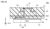
- FIG. 16 is a side perspective view of an antenna module 100K according to embodiment 10.
- the antenna module 100K further includes an auxiliary electrode 154 and a via V2.
- the description of elements that overlap with the antenna module 100 will not be repeated.
- the via V2 is connected to the radiating element 121 at a position offset from the center of the radiating element 121 on the opposite side to the power supply point SP1 (positive direction of the X-axis).
- the via V2 extends in a direction from the radiating element 121 toward the ground electrode GND.
- the auxiliary electrode 154 is connected to the lower end of the via V2.
- the auxiliary electrode 154 is a rectangular flat electrode, and is disposed in a layer between the radiating element 121 and the ground electrode GND.
- the auxiliary electrode 154 extends from the connection position with the via V2 toward the positive direction of the X-axis (fifth direction). When viewed in a plan view from the normal direction of the dielectric substrate 130, it protrudes from the end of the radiating element 121 toward the positive direction of the X-axis.
- This auxiliary electrode 154 allows some of the electric field lines generated from the end of the radiating element 121 in the positive direction of the X-axis to pass through the auxiliary electrode 154 and reach the ground electrode GND.
- the auxiliary electrode 154 in the opposite direction to the auxiliary electrode 150, it is possible to induce the electric field lines at a position closer to the radiating element 121 than in the case where the auxiliary electrode 154 is not present.
- auxiliary electrode 154" in the tenth embodiment corresponds to the "sixth electrode” in this disclosure.
- via V2" in the tenth embodiment corresponds to the "second via” in this disclosure.
- FIG. 17 is a side perspective view of an antenna module 100L according to embodiment 11.
- the antenna module 100L further includes a dielectric lens 180.
- the description of elements that overlap with the antenna module 100 will not be repeated.
- the dielectric lens 180 is a dielectric having a curved convex portion that protrudes in the positive direction of the Z axis.
- the dielectric lens 180 is disposed on the main surface 131 of the dielectric substrate 130, and covers the radiating element 121 when viewed in a plan view from the normal direction of the dielectric substrate 130.
- the convex portion of the dielectric lens 180 is formed in a spherical or aspherical shape, and has the function of concentrating radio waves at a specific focal position by utilizing the refraction of radio waves due to the difference in dielectric constant in the curved shape.
- the focal position can be adjusted by changing the dielectric constant of the dielectric lens 180. Note that differences in the dielectric constant between the dielectric lens 180 and the dielectric substrate 130, and between the dielectric lens 180 and space (air) can cause reflection of radio waves at the interface. Therefore, when materials with a small difference in dielectric constant are used, the reflection loss that occurs at the interface can be reduced.
- the effective wavelength within the dielectric lens 180 becomes shorter and the refractive index at the interface becomes larger, making it possible to reduce the size compared to when a material with a relatively low dielectric constant is used.
- High-frequency signals in the sub-terahertz frequency band tend to be more difficult to secure antenna gain for than signals in lower frequency bands. Therefore, by placing such a dielectric lens 180, it is possible to concentrate the radiated radio waves and increase the antenna gain.
- the concentration of the antenna gain can be increased.
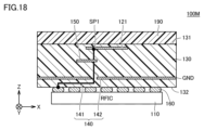
- FIG. 18 is a side perspective view of an antenna module 100M according to embodiment 12.
- the antenna module 100M further includes a dielectric 190 disposed on the main surface 131 of the dielectric substrate 130.
- the description of elements that overlap with the antenna module 100 will not be repeated.
- the dielectric 190 has a dielectric constant different from that of the dielectric substrate 130, and is disposed over the entire surface of the main surface 131. In other words, when viewed in a plan view from the normal direction of the dielectric substrate 130, the dielectric 190 covers the radiating element 121.
- the surface waves of the electric field propagating on the surface of the dielectric substrate 130 are affected by the dielectric constant of the dielectric material that constitutes the dielectric substrate 130.
- the dielectric constant of the substrate is relatively high, the surface waves spread more than when the dielectric constant is low.
- the spread of the surface wave can be increased, and the frequency band can be expanded.
- the effect of surface waves causes the frequency band to become excessively wide and the desired antenna gain cannot be ensured, the effect of surface waves can be reduced and the antenna gain increased by using a material for dielectric 190 that has a lower dielectric constant than that of dielectric substrate 130.
- the dielectric constant of the dielectric 190 is appropriately selected taking into consideration the required frequency bandwidth, antenna gain, and the dielectric constant of the dielectric used in the dielectric substrate 130, etc.
- the directivity of the antenna module can be improved by providing an auxiliary electrode in the via of the power supply wiring.
- An antenna module includes a dielectric substrate, a flat-plate-shaped first radiating element, a ground electrode, a first power supply wiring, and a flat-plate-shaped first electrode.
- the dielectric substrate has a first main surface and a second main surface that face each other.
- the first radiating element is disposed on the dielectric substrate.
- the ground electrode is disposed on the dielectric substrate closer to the second main surface than the first radiating element and facing the first radiating element.
- the first power supply wiring transmits a high-frequency signal to a first power supply point of the first radiating element.
- the first electrode is connected to the first power supply wiring and disposed between the first radiating element and the ground electrode.
- the first power supply point is disposed at a position offset from the center of the first radiating element in the first direction. When viewed in a plan view from the normal direction of the dielectric substrate, the first electrode protrudes from the first radiating element in the first direction.
- the amount of protrusion of the first electrode from the first radiating element is less than or equal to half the dimension of the first radiating element in the first direction.
- the first electrode includes a first portion protruding from the first radiating element and a second portion overlapping the first radiating element when viewed in a plan view from the normal direction of the dielectric substrate.
- the dimension of the first portion in the second direction is 1/10 or more and 2/3 or less of the dimension of the first radiating element in the first direction.
- the dimension in the second direction of the first portion is greater than the dimension in the second direction of the second portion.
- the antenna module described in any one of 1 to 4 further includes a second electrode connected in the first power supply wiring between the first electrode and the ground electrode. When viewed in a plan view from the normal direction of the dielectric substrate, the second electrode protrudes from the first electrode in the first direction.
- the antenna module described in any one of paragraphs 1 to 4 further includes a first via extending from the first electrode toward the ground electrode, and a flat third electrode connected to the first via. When viewed in a plan view from the normal direction of the dielectric substrate, the third electrode protrudes from the first electrode in the first direction.
- the antenna module described in any one of 1 to 6 further includes a second power supply wiring and a flat-plate-shaped fourth electrode.
- the second power supply wiring supplies a high-frequency signal to a second power supply point that is disposed at a position offset in the third direction from the center of the first radiating element.
- the fourth electrode is connected to the second power supply wiring.
- the third direction intersects with the first direction.
- the fourth electrode is connected to the second power supply wiring between the first radiating element and the ground electrode. When viewed in a plan view from the normal direction of the dielectric substrate, the fourth electrode protrudes from the first radiating element in the third direction.
- the antenna module according to any one of 1 to 6 further includes a second radiating element, a third feeding line, and a fifth electrode.
- the second radiating element is disposed between the first electrode and the ground electrode, and overlaps with the first radiating element when viewed in a plan view from the normal direction of the dielectric substrate.
- the third feeding line transmits a high-frequency signal to a third feeding point that is disposed at a position offset in the fourth direction from the center of the second radiating element.
- the fifth electrode is connected to the third feeding line and disposed between the second radiating element and the ground electrode.
- the dimensions of the second radiating element are larger than the dimensions of the first radiating element. When viewed in a plan view from the normal direction of the dielectric substrate, the fifth electrode protrudes from the second radiating element in the fourth direction.
- the antenna module described in any one of clauses 1 to 6 further includes a second via and a flat-plate-shaped sixth electrode.
- the second via is connected to the first radiating element at a position offset from the center of the first radiating element in a fifth direction opposite to the first direction.
- the sixth electrode is connected to the second via and is disposed between the first radiating element and the ground electrode. When viewed in a plan view from the normal direction of the dielectric substrate, the sixth electrode protrudes from the first radiating element in the fifth direction.
- the antenna module described in any one of paragraphs 1 to 9 further includes a grounding member that is disposed around the first radiating element so as to surround the first radiating element when viewed in a plan view from the normal direction of the dielectric substrate, and is electrically connected to the grounding electrode.
- the antenna module described in any one of paragraphs 1 to 10 further includes a dielectric arranged on the first main surface of the dielectric substrate so as to cover the first radiating element when viewed in a plan view from the normal direction of the dielectric substrate.
- the dielectric constant of the dielectric is different from the dielectric constant of the dielectric substrate.
- the antenna module described in any one of paragraphs 1 to 10 further includes a dielectric lens disposed on the first main surface of the dielectric substrate and having a convex shape in the normal direction. When viewed in a plan view from the normal direction of the dielectric substrate, the dielectric lens covers the first radiating element.
- the first radiating element has a substantially rectangular shape when viewed in a plan view from the normal direction of the dielectric substrate.
- the first radiating element has a generally cross shape with protrusions protruding along the first and second directions when viewed in a plan view from the normal direction of the dielectric substrate.
- the protrusion of the first electrode has a tapered shape that narrows toward the center of the first radiating element.
- the first radiating element has a substantially circular shape when viewed in a plan view from the normal direction of the dielectric substrate.
- the antenna module described in any one of paragraphs 1 to 17 includes a third radiating element having a flat plate shape, a fourth power supply wiring, and a seventh electrode having a flat plate shape.
- the third radiating element is disposed adjacent to the first radiating element when viewed from a plane in the normal direction of the dielectric substrate, and is disposed opposite the ground electrode.
- the fourth power supply wiring transmits a high frequency signal to a fourth power supply point of the third radiating element.
- the seventh electrode is connected to the fourth power supply wiring and is disposed between the third radiating element and the ground electrode.
- the fourth power supply point is disposed at a position offset from the center of the third radiating element in the first direction. When viewed from a plane in the normal direction of the dielectric substrate, the seventh electrode protrudes from the third radiating element in the first direction.
- the antenna module described in any one of paragraphs 1 to 18 further includes a power supply circuit that supplies a high-frequency signal to each radiating element.
- a communication device is equipped with an antenna module as described in any one of the first to 19th paragraphs.
Landscapes
- Waveguide Aerials (AREA)
Priority Applications (2)
| Application Number | Priority Date | Filing Date | Title |
|---|---|---|---|
| CN202480056700.4A CN121816671A (zh) | 2023-09-28 | 2024-08-15 | 天线模块和搭载该天线模块的通信装置 |
| JP2025548576A JPWO2025069764A1 (https=) | 2023-09-28 | 2024-08-15 |
Applications Claiming Priority (2)
| Application Number | Priority Date | Filing Date | Title |
|---|---|---|---|
| JP2023168456 | 2023-09-28 | ||
| JP2023-168456 | 2023-09-28 |
Publications (1)
| Publication Number | Publication Date |
|---|---|
| WO2025069764A1 true WO2025069764A1 (ja) | 2025-04-03 |
Family
ID=95203634
Family Applications (1)
| Application Number | Title | Priority Date | Filing Date |
|---|---|---|---|
| PCT/JP2024/029055 Pending WO2025069764A1 (ja) | 2023-09-28 | 2024-08-15 | アンテナモジュールおよびそれを搭載した通信装置 |
Country Status (3)
| Country | Link |
|---|---|
| JP (1) | JPWO2025069764A1 (https=) |
| CN (1) | CN121816671A (https=) |
| WO (1) | WO2025069764A1 (https=) |
Citations (3)
| Publication number | Priority date | Publication date | Assignee | Title |
|---|---|---|---|---|
| US4755820A (en) * | 1985-08-08 | 1988-07-05 | The Secretary Of State For Defence In Her Britannic Majesty's Government Of The United Kingdom Of Great Britain And Northern Ireland | Antenna device |
| JP2015008410A (ja) * | 2013-06-25 | 2015-01-15 | パナソニックIpマネジメント株式会社 | 無線モジュール |
| WO2019189050A1 (ja) * | 2018-03-30 | 2019-10-03 | 株式会社村田製作所 | アンテナモジュールおよびそれを搭載した通信装置 |
-
2024
- 2024-08-15 JP JP2025548576A patent/JPWO2025069764A1/ja active Pending
- 2024-08-15 WO PCT/JP2024/029055 patent/WO2025069764A1/ja active Pending
- 2024-08-15 CN CN202480056700.4A patent/CN121816671A/zh active Pending
Patent Citations (3)
| Publication number | Priority date | Publication date | Assignee | Title |
|---|---|---|---|---|
| US4755820A (en) * | 1985-08-08 | 1988-07-05 | The Secretary Of State For Defence In Her Britannic Majesty's Government Of The United Kingdom Of Great Britain And Northern Ireland | Antenna device |
| JP2015008410A (ja) * | 2013-06-25 | 2015-01-15 | パナソニックIpマネジメント株式会社 | 無線モジュール |
| WO2019189050A1 (ja) * | 2018-03-30 | 2019-10-03 | 株式会社村田製作所 | アンテナモジュールおよびそれを搭載した通信装置 |
Non-Patent Citations (1)
| Title |
|---|
| ALIAKBARI HANIEH, MOSALANEJAD MOHAMMAD, SOENS CHARLOTTE, VANDENBOSCH GUY, LAU BUON KIONG: "79 GHz Multilayer Series-Fed Patch Antenna Array With Stacked Micro-Via Loading", IEEE ANTENNAS AND WIRELESS PROPAGATION LETTERS, IEEE, PISCATAWAY, NJ, US, vol. 21, no. 10, 1 October 2022 (2022-10-01), US , pages 1990 - 1994, XP093296919, ISSN: 1536-1225, DOI: 10.1109/LAWP.2022.3187764 * |
Also Published As
| Publication number | Publication date |
|---|---|
| CN121816671A (zh) | 2026-04-07 |
| JPWO2025069764A1 (https=) | 2025-04-03 |
Similar Documents
| Publication | Publication Date | Title |
|---|---|---|
| JP6760541B2 (ja) | アンテナモジュールおよびそれを搭載した通信装置 | |
| CN114521307B (zh) | 天线模块和搭载该天线模块的通信装置以及电路基板 | |
| WO2019189050A1 (ja) | アンテナモジュールおよびそれを搭載した通信装置 | |
| CN113302799B (zh) | 天线模块和搭载该天线模块的通信装置 | |
| JP7294525B2 (ja) | アンテナモジュールおよびそれを搭載する通信装置 | |
| WO2023047801A1 (ja) | アンテナモジュールおよびそれを搭載する通信装置 | |
| WO2022176646A1 (ja) | アンテナモジュールおよびアレイアンテナ | |
| JP7740575B2 (ja) | アンテナモジュールおよびそれを搭載した通信装置 | |
| US20250149788A1 (en) | Antenna module and communication apparatus including the same | |
| WO2022185874A1 (ja) | アンテナモジュールおよびそれを搭載した通信装置 | |
| US20240313426A1 (en) | Antenna module and communication device equipped with the same | |
| WO2025069764A1 (ja) | アンテナモジュールおよびそれを搭載した通信装置 | |
| WO2025069765A1 (ja) | アンテナモジュールおよびそれを搭載した通信装置 | |
| CN115136413B (zh) | 天线模块以及搭载有天线模块的通信装置 | |
| WO2022230383A1 (ja) | アンテナモジュールおよびそれを搭載した通信装置 | |
| JP7810257B2 (ja) | アンテナモジュール | |
| JP7852743B2 (ja) | アンテナモジュールおよびそれを搭載した通信装置 | |
| WO2025164533A1 (ja) | アンテナ装置、アンテナモジュール、および通信装置 | |
| JP2024107757A (ja) | アンテナモジュールおよびそれを搭載した通信装置 | |
| WO2023188969A1 (ja) | アンテナモジュール | |
| WO2026079006A1 (ja) | アンテナモジュールおよびそれを搭載した通信装置 | |
| WO2025150415A1 (ja) | アンテナモジュールおよびそれを搭載した通信装置、ならびに、アンテナモジュールの製造方法 | |
| WO2026053546A1 (ja) | アンテナモジュールおよびそれを搭載した通信装置 | |
| WO2026018620A1 (ja) | アンテナモジュールおよびそれを搭載した通信装置 | |
| WO2024135047A1 (ja) | アンテナモジュールおよびそれを搭載した通信装置 |
Legal Events
| Date | Code | Title | Description |
|---|---|---|---|
| 121 | Ep: the epo has been informed by wipo that ep was designated in this application |
Ref document number: 24871566 Country of ref document: EP Kind code of ref document: A1 |
|
| ENP | Entry into the national phase |
Ref document number: 2025548576 Country of ref document: JP Kind code of ref document: A |
|
| WWE | Wipo information: entry into national phase |
Ref document number: 2025548576 Country of ref document: JP |