WO2025069381A1 - 量子デバイス - Google Patents
量子デバイス Download PDFInfo
- Publication number
- WO2025069381A1 WO2025069381A1 PCT/JP2023/035657 JP2023035657W WO2025069381A1 WO 2025069381 A1 WO2025069381 A1 WO 2025069381A1 JP 2023035657 W JP2023035657 W JP 2023035657W WO 2025069381 A1 WO2025069381 A1 WO 2025069381A1
- Authority
- WO
- WIPO (PCT)
- Prior art keywords
- line
- filter
- resonators
- quantum
- lines
- Prior art date
- Legal status (The legal status is an assumption and is not a legal conclusion. Google has not performed a legal analysis and makes no representation as to the accuracy of the status listed.)
- Ceased
Links
Images





Classifications
-
- H—ELECTRICITY
- H10—SEMICONDUCTOR DEVICES; ELECTRIC SOLID-STATE DEVICES NOT OTHERWISE PROVIDED FOR
- H10N—ELECTRIC SOLID-STATE DEVICES NOT OTHERWISE PROVIDED FOR
- H10N69/00—Integrated devices, or assemblies of multiple devices, comprising at least one superconducting element covered by group H10N60/00
-
- H—ELECTRICITY
- H10—SEMICONDUCTOR DEVICES; ELECTRIC SOLID-STATE DEVICES NOT OTHERWISE PROVIDED FOR
- H10N—ELECTRIC SOLID-STATE DEVICES NOT OTHERWISE PROVIDED FOR
- H10N60/00—Superconducting devices
- H10N60/10—Junction-based devices
-
- H—ELECTRICITY
- H10—SEMICONDUCTOR DEVICES; ELECTRIC SOLID-STATE DEVICES NOT OTHERWISE PROVIDED FOR
- H10N—ELECTRIC SOLID-STATE DEVICES NOT OTHERWISE PROVIDED FOR
- H10N60/00—Superconducting devices
- H10N60/10—Junction-based devices
- H10N60/12—Josephson-effect devices
Definitions
- This disclosure relates to quantum devices.
- a quantum device has been proposed in which multiple quantum bits are coupled to one readout port via a resonator and a filter.
- parasitic capacitances tend to differ between multiple resonators.
- the objective of this disclosure is to provide a quantum device that can suppress the variation in the parasitic capacitance of a resonator.
- a quantum device has a plurality of superconducting quantum bits, a plurality of resonators capacitively coupled to each of the plurality of superconducting quantum bits, a filter coupled to the plurality of resonators, and a port capacitively coupled to the filter, where the shortest distance between the port and the resonator is equal among the plurality of resonators.
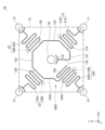
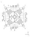
- FIG. 1 is a plan view showing the quantum device according to the first embodiment.
- FIG. 2 is a plan view showing a quantum device according to a reference example.
- FIG. 3 is a diagram showing the calculation results of the resonance frequency.
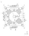
- FIG. 4 is a plan view showing the quantum device according to the second embodiment.
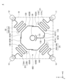
- FIG. 5 is a plan view showing a quantum device according to the third embodiment.
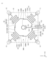
- FIG. 6 is a plan view showing a quantum device according to the fourth embodiment.
- FIG. 7 is a plan view showing a quantum device according to the fifth embodiment.
- FIG. 8 is a plan view showing a quantum device according to the sixth embodiment.
- FIG. 9 is a plan view showing a quantum device according to the seventh embodiment.
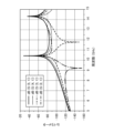
- FIG. 10 is a diagram showing the results of a simulation of a quantum device according to a reference example.
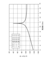
- FIG. 11 is a diagram showing the results of a simulation of the quantum device according to the fourth embodiment.
- FIG. 12 is a diagram showing the results of a simulation of the quantum device according to the sixth embodiment.
- an XYZ Cartesian coordinate system is used, but this coordinate system is defined for the purpose of explanation and does not limit the attitude of the quantum device.
- the +Z side may be referred to as the upper side, top, or top
- the -Z side may be referred to as the lower side, bottom, or bottom.
- a planar view refers to viewing an object from the +Z side
- a planar shape refers to the shape of an object viewed from the +Z side.
- a first embodiment relates to a quantum device.
- Fig. 1 is a plan view showing a quantum device according to the first embodiment.
- the quantum device 1 has quantum bits 11, 12, 13, and 14.
- the quantum bits 11 to 14 are superconducting quantum bits, and include, for example, Josephson junctions.
- the quantum bits 11 to 14 are at the vertices of a square 10 in a plan view.
- the X coordinates of the quantum bits 11 and 12 are the same, and the X coordinates of the quantum bits 13 and 14 are the same.
- the Y coordinates of the quantum bits 11 and 14 are the same, and the Y coordinates of the quantum bits 12 and 13 are the same.
- the quantum bit 11 is on the +X side of the quantum bit 14, and the quantum bit 12 is on the +X side of the quantum bit 13.
- the quantum bit 12 is on the +Y side of the quantum bit 11, and the quantum bit 13 is on the +Y side of the quantum bit 14.
- the quantum bits 11 to 14 have a resonant frequency of, for example, 3-10 GHz.
- the quantum device 1 has a read port 30.
- the read port 30 is at the center of the square 10.
- the read port 30 has, for example, a circular metal film.
- Quantum device 1 has resonators 21, 22, 23, and 24.
- Resonator 21 has a base 21A and a resonant frequency adjustment section 21B connected to base 21A.
- Resonator 22 has a base 22A and a resonant frequency adjustment section 22B connected to base 22A.
- Resonator 23 has a base 23A and a resonant frequency adjustment section 23B connected to base 23A.
- Resonator 24 has a base 24A and a resonant frequency adjustment section 24B connected to base 24A.
- bases 21A, 22A, 23A, and 24A are identical to each other. That is, in a planar view, bases 21A, 22A, 23A, and 24A are congruent.
- Bases 21A, 22A, 23A, and 24A include lines having a meandering shape.
- Base 21A has a portion that extends perpendicular to the line segment connecting readout port 30 and quantum bit 11.
- Base 22A has a portion that extends perpendicular to the line segment connecting readout port 30 and quantum bit 12.
- Base 23A has a portion that extends perpendicular to the line segment connecting readout port 30 and quantum bit 13.
- Base 24A has a portion that extends perpendicular to the line segment connecting readout port 30 and quantum bit 14.
- Base 21A is capacitively coupled to quantum bit 11.
- Base 22A is capacitively coupled to quantum bit 12.
- Base 23A is capacitively coupled to quantum bit 13.
- Base 24A is capacitively coupled to quantum bit 14.
- Bases 21A, 22A, 23A, and 24A are arranged to have four-fold rotational symmetry around readout port 30. The shortest distance between readout port 30 and each of bases 21A, 22A, 23A, and 24A is equal among resonators 21 to 24.
- the resonance frequency adjustment units 21B, 22B, 23B, and 24B have lines with slightly different path lengths. These lines are shorted to the ground line.
- the resonance frequencies differ slightly among the resonators 21 to 24.
- the resonance frequency of the resonator 21 is 10.1 GHz
- the resonance frequency of the resonator 22 is 10.2 GHz
- the resonance frequency of the resonator 23 is 10.3 GHz
- the resonance frequency of the resonator 24 is 10.4 GHz.
- Each of the resonance frequency adjustment units 21B, 22B, 23B, and 24B is away from the portion of each of the bases 21A, 22A, 23A, and 24A that is closest to the readout port 30.
- the shortest distance between the readout port 30 and each of the resonators 21 to 24 is equal among the resonators 21 to 24.
- Quantum device 1 has filter 100.
- Filter 100 is coupled to resonators 21 to 24.
- filter 100 is capacitively coupled to resonators 21 to 24.
- read port 30 is capacitively coupled to filter 100.
- Filter 100 has lines 110, 120, 130, 140, 150, 121, 122, 123, 124, 131, and 132.
- Line 131 is provided near read port 30 and has a planar shape that follows the outer edge of read port 30.
- the planar shape of line 131 is, for example, an arc.
- Line 131 is on the -Y side of read port 30.
- Line 132 is connected to line 131 and extends from line 131 to the -Y side along the Y axis.
- Line 121 is connected to line 132 and extends from the -Y end of line 132 to the +X side along the X axis.
- Line 110 is connected to line 121 and extends from the +X end of line 121 to the +X and +Y sides perpendicular to the line segment connecting readout port 30 and quantum bit 11, and intersects with the line segment connecting readout port 30 and quantum bit 11.
- Line 122 is connected to line 110 and extends from the +X and +Y ends of line 110 to the +Y side along the Y axis.
- Line 120 is connected to line 122 and extends from the +Y end of line 122 to the -X and +Y sides perpendicular to the line segment connecting readout port 30 and quantum bit 12, and intersects with the line segment connecting readout port 30 and quantum bit 12.
- the line 123 is connected to the line 120 and extends from the end of the line 120 on the -X side and the +Y side to the -X side along the X axis.
- the line 130 is connected to the line 123 and extends from the end of the line 123 on the -X side to the -X side and the -Y side perpendicular to the line segment connecting the readout port 30 and the quantum bit 13, and intersects with the line segment connecting the readout port 30 and the quantum bit 13.
- the line 124 is connected to the line 130 and extends from the end of the line 130 on the -X side and the -Y side to the -Y side along the Y axis.
- the line 140 is connected to the line 124 and extends from the end of the line 124 on the -Y side to the +X side and the -Y side perpendicular to the line segment connecting the readout port 30 and the quantum bit 14, and intersects with the line segment connecting the readout port 30 and the quantum bit 14.
- Line 150 is connected to line 140 and has a meandering shape that snakes from the +X and -Y ends of line 140 toward read port 30.
- the path length of filter 100 may be about 1 time the wavelength ⁇ . For example, it is about 1/2 the wavelength ⁇ in order to prevent the propagation of photons emitted from the quantum bit at the quantum bit's resonant frequency of 6 GHz. On the other hand, this filter does not prevent the propagation of signals at the resonant frequency of resonators 21-24, for example, 10 GHz.
- the path length of filter 100 is about 1 time or 1/2 the wavelength ⁇ , the end of filter 100 opposite the read port 30 is open.
- the lines 110, 120, 130, and 140 are arranged so as to have four-fold rotational symmetry around the read port 30.
- the shortest distances between the read port 30 and each of the lines 110, 120, 130, and 140 are equal to each other.
- the shortest distances between the line 110 and the base 21A, the shortest distance between the line 120 and the base 22A, the shortest distance between the line 130 and the base 23A, and the shortest distance between the line 140 and the base 24A are equal to each other.
- the states of quantum bits 11 to 14 can be read out simultaneously by inputting a 10 GHz signal to read port 30.
- the states of quantum bits 11 to 14 can be read out simultaneously by frequency-separating the read signal.
- the shortest distance between the read port 30 and each of the resonators 21 to 24 is equal among the resonators 21 to 24. This makes it possible to reduce the difference in parasitic capacitance among the resonators 21 to 24. If the difference in parasitic capacitance is large, the resonant frequencies of the resonators 21 to 24 may easily deviate from the design values. Furthermore, the amount of deviation in the resonant frequencies may differ among the resonators 21 to 24, making frequency separation difficult. According to this embodiment, these problems can be reduced.
- resonators 21 to 24 include, for example, a superconducting thin film, but even if there is unevenness in the thickness of the superconducting thin film, the above-mentioned shortest distance is equal between resonators 21 to 24, so the degree of unevenness in thickness is highly uniform. Therefore, the amount of shift in resonance frequency due to unevenness in thickness is also highly uniform, and frequency separation can be reliably performed even if there is unevenness in the thickness of the superconducting thin film.
- via holes may be formed in the quantum device 1 to suppress chip modes or unwanted modes.
- the via holes may be formed before the resonators 21 to 24, or may be formed after the resonators 21 to 24. If the via holes are formed before the resonators 21 to 24, the thickness of the resist for forming the resonators 21 to 24 may be affected by the via holes. However, since the above-mentioned shortest distance is equal between the resonators 21 to 24, it is easy to obtain high uniformity in the thickness of the resist around the area where the resonators 21 to 24 are formed. Also, if the via holes are formed after the resonators 21 to 24, the thickness of the resist for forming the via holes and the interference during exposure may be affected by the resonators 21 to 24. However, since the above-mentioned shortest distance is equal between the resonators 21 to 24, it is easy to obtain high uniformity in the thickness of the resist around the area where the resonators 21 to 24 are formed and the interference during exposure.
- the filter 100 may be magnetically coupled to the resonators 21 to 24.
- quantum device 1X As shown in FIG. 2, quantum device 1X according to the reference example has filter 100X instead of filter 100, and has resonator 24X instead of resonator 24.
- the other configuration of quantum device 1X is the same as that of quantum device 1.
- Filter 100X has line 124X instead of line 124, and line 140X instead of line 140. Other configurations of filter 100X are the same as those of filter 100.
- Line 124X is shorter than line 124.
- Line 140X extends slightly from the -Y side end of line 124X toward the -X and -Y sides, and from there, like line 140, extends toward the +X and -Y sides perpendicular to the line segment connecting readout port 30 and quantum bit 14, and intersects with the line segment connecting readout port 30 and quantum bit 14.
- Line 150 is connected to line 140X, and has a meandering shape that meanders from the +X and -Y side ends of line 140X toward readout port 30.
- the shortest distance between readout port 30 and line 140X is longer than the shortest distance between readout port 30 and each of lines 110, 120, and 130. Also, the shortest distance between readout port 30 and line 150 is equal to the shortest distance between readout port 30 and each of lines 110, 120, and 130.
- the resonator 24X has a base 24AX and a resonant frequency adjustment section 24B connected to the base 24A.
- the base 24AX includes a line having a meandering shape with a shorter period than the base 24A.
- the shortest distance between the read port 30 and the resonator 24X is longer than the shortest distance between the read port 30 and each of the resonators 21, 22, and 23.
- the other configuration of the resonator 24X is the same as that of the resonator 24.
- the inventors of the present application calculated the resonant frequencies when a quantum device was manufactured according to the first embodiment and the reference example by simulation.
- the resonant frequencies of resonators 21 and 24 were calculated, and in the reference example, the resonant frequencies of resonators 21 and 24X were calculated.
- the designed resonant frequency F1 of resonator 21 was set to 10.18 GHz, and the resonant frequencies of resonators 24 and 24X were set to 10.27.
- FIG. 3 is a diagram showing the calculation results of the resonant frequencies. As shown in FIG.
- the resonant frequencies of resonators 21 and 24 were almost the same as the design values.
- the resonant frequencies of resonators 21 and 24X were higher than the design values.
- a second embodiment differs from the first embodiment mainly in the configuration of the filter.
- Fig. 4 is a plan view showing a quantum device according to the second embodiment.
- the quantum device 2 has a filter 200 instead of the filter 100.
- Filter 200 has lines 222A, 222B, 222C, 222D, and 222E instead of line 122, lines 223A, 223B, 223C, 223D, and 223E instead of line 123, and lines 224A, 224B, 224C, 224D, and 224E instead of line 124.
- Line 222A is connected to line 110 and extends from the +X and +Y ends of line 110 along the Y axis to the +Y side.
- Line 222B is connected to line 222A and extends from the +Y end of line 222A along the X axis to the +X side.
- Line 222C is connected to line 222B and extends from the +X end of line 222B along the Y axis to the +Y side.
- Line 222D is connected to line 222C and extends from the +Y end of line 222C along the X axis to the -X side.
- Line 222E is connected to lines 222D and 120 and extends from the -X end of line 222D along the Y axis to the +Y side.
- lines 222A and 222E are arranged symmetrically with respect to each other, and lines 222B and 222D are arranged symmetrically with respect to each other.
- Line 223A is connected to line 120 and extends from the -X and +Y ends of line 120 along the X axis to the -X side.
- Line 223B is connected to line 223A and extends from the -X end of line 223A along the Y axis to the +Y side.
- Line 223C is connected to line 223B and extends from the +Y end of line 223B along the X axis to the -X side.
- Line 223D is connected to line 223C and extends from the -X end of line 223C along the Y axis to the -Y side.
- Line 223E is connected to lines 223D and 130 and extends from the -Y end of line 223D along the X axis to the -X side.
- Lines 223A and 223E are arranged symmetrically with respect to a line parallel to the Y axis passing through the center of square 10, and lines 223B and 223D are arranged symmetrically with respect to each other.
- Line 224A is connected to line 130 and extends from the -X and -Y ends of line 130 along the Y axis to the -Y side.
- Line 224B is connected to line 224A and extends from the -Y end of line 224A along the X axis to the -X side.
- Line 224C is connected to line 224B and extends from the -X end of line 224B along the Y axis to the -Y side.
- Line 224D is connected to line 224C and extends from the -Y end of line 224C along the X axis to the +X side.
- Line 224E is connected to lines 224D and 140 and extends from the +X end of line 224D along the Y axis to the -Y side. With a straight line parallel to the X-axis passing through the center of square 10 as the axis of symmetry, lines 224A and 224E are arranged symmetrically with respect to each other, and lines 224B and 224D are arranged symmetrically with respect to each other.
- the path length of filter 200 may be approximately 1/2 or 1 time the wavelength ⁇ .
- the path length is approximately 1/2 or 1 time the wavelength ⁇ in order to prevent the propagation of photons emitted from the quantum bit.
- this filter does not prevent the propagation of signals with the resonant frequency of resonators 21 to 24, for example, 10 GHz.
- Filter 200 may also be magnetically coupled to resonators 21 to 24.
- quantum device 2 are the same as those of quantum device 1.
- the quantum device 2 according to the second embodiment can also achieve the same effects as those of the first embodiment.
- a third embodiment differs from the first embodiment mainly in the configuration of the filter.
- Fig. 5 is a plan view showing a quantum device according to the third embodiment.
- the quantum device 3 has a filter 300 instead of the filter 100.
- Filter 300 has lines 321A, 321B, and 321C instead of line 121, lines 322A and 322B instead of line 122, lines 323A and 323B instead of line 123, and lines 324A and 324B instead of line 124.
- Line 321B is connected to line 132 and extends from the -Y side end of line 132 to the +X side and -X side along the X axis.
- Line 321A is connected to line 140 and extends from the +X side and -Y side ends of line 140 to the +X side along the X axis.
- Line 321C is connected to line 110 and extends from the -X side and -Y side ends of line 110 to the -X side along the X axis.
- Lines 321A and 321C are separated from line 321B. Lines 321A, 321B and 321C have the same Y coordinate.
- Lines 321A and 321B are capacitively coupled to each other, and lines 321C and 321B are capacitively coupled to each other.
- the +X end of line 321A, the -X end of line 321B, the +X end of line 321B, and the -X end of line 321C are open ends.
- Lines 321A and 321C are arranged symmetrically with respect to a straight line parallel to the Y axis that passes through the center of square 10.
- Line 322A is connected to line 110 and extends from the end of line 110 on the +X side and +Y side to the +Y side along the Y axis.
- Line 322B is connected to line 120 and extends from the end of line 120 on the +X side and -Y side to the -Y side along the Y axis.
- the X coordinates of lines 322A and 322B are the same.
- Lines 322A and 322B are capacitively coupled to each other.
- the end of line 322A on the +Y side and the end of line 322B on the -Y side are open ends.
- Lines 322A and 322B are arranged symmetrically with respect to a straight line parallel to the X axis that passes through the center of square 10.
- Line 323A is connected to line 120 and extends from the -X and +Y end of line 120 to the -X side along the X axis.
- Line 323B is connected to line 130 and extends from the +X and +Y end of line 130 to the +X side along the X axis.
- the Y coordinates of lines 323A and 323B are the same.
- Lines 323A and 323B are capacitively coupled to each other.
- the -X end of line 323A and the +X end of line 323B are open ends.
- Lines 323A and 323B are arranged symmetrically with respect to a straight line parallel to the Y axis that passes through the center of square 10.
- Line 324A is connected to line 130 and extends from the -X and -Y end of line 130 to the -Y side along the Y axis.
- Line 324B is connected to line 140 and extends from the -X and +Y end of line 140 to the +Y side along the Y axis.
- the X coordinates of lines 324A and 324B are the same.
- Lines 324A and 324B are capacitively coupled to each other.
- the -Y end of line 324A and the +Y end of line 324B are open ends.
- Lines 324A and 324B are arranged symmetrically with respect to a straight line parallel to the X axis that passes through the center of square 10.
- the path length of filter 300 may be approximately 1/2 or 1 times the wavelength ⁇ .
- the path length is approximately 1/2 or 1 time the wavelength ⁇ in order to prevent the propagation of photons emitted from the quantum bit.
- this filter does not prevent the propagation of signals with the resonant frequency of resonators 21 to 24, for example, 10 GHz.
- Filter 300 may also be magnetically coupled to resonators 21 to 24.
- quantum device 3 are the same as those of quantum device 1.
- the quantum device 3 according to the third embodiment can also achieve the same effects as those of the first embodiment.
- filter 300 has multiple lines that are capacitively coupled to each other, which improves isolation and reduces unwanted modes.
- a fourth embodiment differs from the first embodiment mainly in the configuration of the filter.
- Fig. 6 is a plan view showing a quantum device according to the fourth embodiment.
- quantum device 4 has filter 400 instead of filter 100.
- Filter 400 has lines 421A, 421B, and 421C instead of line 121, lines 422A and 422B instead of line 122, lines 423A and 423B instead of line 123, and lines 424A and 424B instead of line 124.
- Line 421B is connected to line 132 and extends from the -Y end of line 132 to the +X side along the X axis.
- Line 421A is connected to line 140 and extends from the +X and -Y end of line 140 to the +X side along the X axis.
- Line 421C is connected to line 110 and extends from the -X and -Y end of line 110 to the -X side along the X axis.
- Lines 421A and 421C are separated from line 421B.
- Lines 421A and 421C have the same Y coordinate.
- the Y coordinate of line 421B is greater than the Y coordinate of lines 421A and 421C.
- Lines 421A and 421C are arranged symmetrically with respect to a straight line parallel to the Y axis that passes through the center of square 10.
- Line 422A is connected to line 110 and extends from the +X and +Y ends of line 110 to the +Y side along the Y axis.
- Line 422B is connected to line 120 and extends from the +X and -Y ends of line 120 to the -Y side along the Y axis.
- the X coordinates of the +X and +Y ends of line 110 and line 422A are smaller than the X coordinates of the +X and -Y ends of line 120 and line 422B.
- a part of line 422A overlaps with a part of line 422B, and line 422A and line 422B are capacitively coupled to each other.
- the +Y end of line 422A and the -Y end of line 422B are open ends.
- Line 423A is connected to line 120 and extends from the -X and +Y ends of line 120 to the -X side along the X axis.
- Line 423B is connected to line 130 and extends from the +X and +Y ends of line 130 to the +X side along the X axis.
- the Y coordinates of the -X and +Y ends of line 120 and line 423A are smaller than the Y coordinates of the +X and +Y ends of line 130 and line 423B.
- a part of line 423A overlaps with a part of line 423B, and line 423A and line 423B are capacitively coupled to each other.
- the -X end of line 423A and the +X end of line 423B are open ends.
- Line 424A is connected to line 130 and extends from the -X and -Y ends of line 130 to the -Y side along the Y axis.
- Line 424B is connected to line 140 and extends from the -X and +Y ends of line 140 to the +Y side along the Y axis.
- the X coordinates of the -X and -Y ends of line 130 and line 424A are greater than the X coordinates of the -X and +Y ends of line 140 and line 424B.
- a part of line 424A overlaps with a part of line 424B, and line 424A and line 424B are capacitively coupled to each other.
- the -Y end of line 424A and the +Y end of line 424B are open ends.
- the path length of filter 400 may be approximately 1/2 or 1 times the wavelength ⁇ .
- the path length is approximately 1/2 or 1 time the wavelength ⁇ in order to prevent the propagation of photons emitted from the quantum bit.
- this filter does not prevent the propagation of signals with the resonant frequency of resonators 21 to 24, for example, 10 GHz.
- Filter 400 may also be magnetically coupled to resonators 21 to 24.
- quantum device 4 are the same as those of quantum device 1.
- the quantum device 4 according to the fourth embodiment can also achieve the same effects as those of the third embodiment.
- the capacitively coupled lines within the filter 400 have overlapping portions when viewed from the X-axis direction or the Y-axis direction. This makes it easier to control the direction in which signals are transmitted within the filter 400.
- the quantum device 5 has a filter 500 instead of the filter 400.
- the filter 500 differs from the filter 400 in that the path length from the line 131 to the line 421A is shorter than that of the fourth embodiment, and furthermore, the filter 500 has a line 521D.
- the line 521D is capacitively coupled to the line 421A. Both ends of the line 521D are open ends.
- the path length of the filter 500 may be about 1/2 or 1 time the wavelength ⁇ .
- the path length is about 1/2 or 1 time the wavelength ⁇ in order to prevent the propagation of photons emitted from the quantum bit.
- this filter does not prevent the propagation of signals with frequencies resonating with the resonators 21 to 24, for example, 10 GHz.
- quantum device 5 are the same as those of quantum device 4.
- the quantum device 5 according to the fifth embodiment can also achieve the same effects as those of the fourth embodiment.
- a sixth embodiment differs from the first embodiment mainly in the configuration of the filter.
- Fig. 8 is a plan view showing a quantum device according to the sixth embodiment.
- the quantum device 6 has a filter 600 instead of the filter 100.
- Filter 600 has lines 621A, 621B, 621C, and 621D instead of line 621, lines 622A, 622B, 622C, and 622D instead of line 122, lines 623A, 623B, 623C, and 623D instead of line 123, and lines 624A, 624B, 624C, and 624D instead of line 124.
- Filter 600 further has lines 633 and 644.
- Line 633 is provided near read port 30 and has a planar shape that follows the outer edge of read port 30.
- the planar shape of line 633 is, for example, an arc shape.
- Line 633 is on the +Y side of read port 30.
- Line 634 is connected to line 633 and extends from line 633 to the +Y side along the Y axis.
- Line 621A is connected to line 140 and extends from the end of line 140 on the +X side and the -Y side to the +X side along the X axis.
- Line 621B is connected to line 621A and extends from the end of line 621A on the +X side to the +Y side along the Y axis.
- Line 621D is connected to line 110 and extends from the end of line 110 on the -X side and the -Y side to the -X side along the X axis.
- Line 621C is connected to line 621D and extends from the end of line 621D on the -X side to the +Y side along the Y axis. Lines 621A and 621D have the same Y coordinate.
- the X coordinate of line 621B is smaller than the X coordinate of line 132.
- line 621B and part of line 132 overlap, and line 621B and line 132 are capacitively coupled to each other.
- the X coordinate of line 621C is greater than the X coordinate of line 132.
- line 621C overlaps with a portion of line 132, and line 621C and line 132 are capacitively coupled to each other.
- the +Y side end of line 621B and the +Y side end of line 621C are open ends.
- Lines 621A and 621D are arranged line-symmetrically with respect to a straight line parallel to the Y axis passing through the center of square 10, and lines 621B and 621C are arranged line-symmetrically with respect to each other.
- Line 622A is connected to line 110 and extends from the +X and +Y end of line 110 to the +Y side along the Y axis.
- Line 622B is connected to line 622A and extends from the +Y end of line 622A to the -X side along the X axis.
- Line 622D is connected to line 120 and extends from the +X and -Y end of line 120 to the -Y side along the Y axis.
- Line 622C is connected to line 622D and extends from the -Y end of line 622D to the -X side along the X axis.
- the X coordinates of lines 622A and 622D are the same.
- the Y coordinate of line 622B is smaller than the X coordinate of line 622C.
- lines 622B and 622C When viewed from the Y-axis direction, lines 622B and 622C overlap, and lines 622B and 622C are capacitively coupled to each other.
- the -X side end of line 622B and the -X side end of line 622C are open ends.
- Lines 622A and 622D are arranged line-symmetrically with respect to a straight line parallel to the X-axis that passes through the center of square 10, and lines 622B and 622C are arranged line-symmetrically with respect to each other.
- Line 623A is connected to line 120 and extends from the -X and +Y end of line 120 to the -X side along the X axis.
- Line 623B is connected to line 623A and extends from the -X end of line 623A to the -Y side along the Y axis.
- Line 623D is connected to line 130 and extends from the +X and +Y end of line 130 to the +X side along the X axis.
- Line 623C is connected to line 623D and extends from the +X end of line 623D to the -Y side along the Y axis.
- Lines 623A and 623D have the same Y coordinate.
- the X coordinate of line 623B is greater than the X coordinate of line 634.
- Line 623B and part of line 634 overlap, and line 623B and line 634 are capacitively coupled to each other.
- the X coordinate of line 623C is smaller than the X coordinate of line 634.
- line 623C and part of line 634 overlap, and line 623C and line 634 are capacitively coupled to each other.
- the -Y side end of line 623B and the -Y side end of line 623C are open ends.
- Lines 623A and 623D are arranged line-symmetrically with respect to a straight line parallel to the Y axis that passes through the center of square 10, and lines 623B and 623C are arranged line-symmetrically with respect to each other.
- Line 624A is connected to line 130 and extends from the -X and -Y end of line 130 along the Y axis to the -Y side.
- Line 624B is connected to line 624A and extends from the -Y end of line 624A along the X axis to the +X side.
- Line 624D is connected to line 140 and extends from the -X and +Y end of line 140 along the Y axis to the +Y side.
- Line 624C is connected to line 624D and extends from the +Y end of line 624D along the X axis to the +X side.
- the X coordinates of lines 624A and 624D are the same.
- the Y coordinate of line 624B is greater than the X coordinate of line 624C.
- lines 624B and 624C When viewed from the Y-axis direction, lines 624B and 624C overlap, and lines 624B and 624C are capacitively coupled to each other.
- the +X side end of line 624B and the +X side end of line 624C are open ends.
- Lines 624A and 624D are arranged line-symmetrically with respect to a straight line parallel to the X-axis that passes through the center of square 10, and lines 624B and 624C are arranged line-symmetrically with respect to each other.
- quantum device 6 The rest of the configuration of quantum device 6 is the same as that of quantum device 1.
- the quantum device 6 according to the sixth embodiment can also achieve the same effects as those of the third embodiment.
- the filter 600 has a higher symmetry in a planar view, so that the uniformity of the parasitic capacitances of resonators 21 to 24 can be improved.
- a seventh embodiment differs from the sixth embodiment mainly in the configuration of the filter.
- Fig. 9 is a plan view showing a quantum device according to the seventh embodiment.
- quantum device 7 has filter 700 instead of filter 600.
- Filter 700 further differs from filter 600 in that it has lines 735, 736, 737, and 738.
- Line 735 is provided near read port 30 and has a planar shape that follows the outer edge of read port 30.
- the planar shape of line 735 is, for example, an arc shape.
- Line 735 is on the +X side of read port 30.
- Line 736 is connected to line 735 and extends from line 735 to the +X side along the X-axis. When viewed from the Y-axis direction, lines 622B and 622C overlap with a portion of line 736, and lines 622B and 622C are capacitively coupled to line 736.
- Line 737 is provided near read port 30 and has a planar shape that follows the outer edge of read port 30.
- the planar shape of line 737 is, for example, an arc shape.
- Line 737 is on the -X side of read port 30.
- Line 738 is connected to line 737 and extends from line 737 to the -X side along the X-axis. When viewed from the Y-axis direction, lines 624B and 624C overlap with a portion of line 738, and lines 624B and 624C are capacitively coupled to line 738.
- quantum device 7 The rest of the configuration of quantum device 7 is the same as that of quantum device 6.
- the quantum device 7 according to the seventh embodiment can also achieve the same effects as those of the sixth embodiment.
- the filter 700 has a higher symmetry in a planar view, so that the uniformity of the parasitic capacitances of resonators 21 to 24 can be further improved.
- the inventors of the present application performed a simulation of quantum devices 1X, 4, and 6.
- the transmittance was calculated as an S parameter for a superconducting circuit simulating quantum devices 1X, 4, and 6, with readout port 30 as the first port, quantum bit 11 as the second port, quantum bit 12 as the third port, quantum bit 13 as the fourth port, and quantum bit 14 as the fifth port.
- the coupling capacitance between readout port 30 and each filter was set to 5.5 fF
- the coupling capacitance between the lines in filters 400 and 600 was set to 50 fF.
- FIG. 10 is a diagram showing the results of a simulation of quantum device 1X according to a reference example.
- FIG. 11 is a diagram showing the results of a simulation of quantum device 4 according to the fourth embodiment.
- FIG. 12 is a diagram showing the results of a simulation of quantum device 6 according to the sixth embodiment.
- "dB(S(A,1))" in FIGS. 10 to 12 indicates the transmittance at port A when a signal is input from port 1.
- filter 400 has multiple lines that are capacitively coupled to each other, improving the isolation between resonators 21 to 24.
- the eigenmode frequencies of the quantum bits 11 to 14 are aligned with the eigenmode frequencies of the resonators 21 to 24.
- the eigenmode frequencies of the resonators are multiplexed to read out the state, so the eigenmode frequencies may be detuned between the quantum bits and between the resonators. In this case, the same effect can be expected.
- the path length of the filter is not particularly limited.
- the path length of the filter may be about 1/4 of the wavelength corresponding to the frequency at which the multiple resonators resonate, and the filter may be a coplanar waveguide filter.
- the tip of the filter is shorted to the ground line.
- the end of the filter opposite the port side is shorted.
- the filter may be a band-pass filter or a filter that attenuates signals in a specific frequency band.
- the filter is not limited to a coplanar waveguide filter, and a microstrip waveguide filter or the like may be used.
- the number of quantum bits coupled to one port is not particularly limited. It is preferable that the quantum bits coupled to one port are located at the vertices of a regular polygon centered on the port.
- the quantum device disclosed herein can be used, for example, in quantum computing.
- quantum device 10 square 11
Landscapes
- Control Of Motors That Do Not Use Commutators (AREA)
Priority Applications (3)
| Application Number | Priority Date | Filing Date | Title |
|---|---|---|---|
| PCT/JP2023/035657 WO2025069381A1 (ja) | 2023-09-29 | 2023-09-29 | 量子デバイス |
| EP23954350.7A EP4788109A1 (en) | 2023-09-29 | 2023-09-29 | Quantum device |
| JP2025548394A JPWO2025069381A1 (cg-RX-API-DMAC7.html) | 2023-09-29 | 2023-09-29 |
Applications Claiming Priority (1)
| Application Number | Priority Date | Filing Date | Title |
|---|---|---|---|
| PCT/JP2023/035657 WO2025069381A1 (ja) | 2023-09-29 | 2023-09-29 | 量子デバイス |
Publications (1)
| Publication Number | Publication Date |
|---|---|
| WO2025069381A1 true WO2025069381A1 (ja) | 2025-04-03 |
Family
ID=95203134
Family Applications (1)
| Application Number | Title | Priority Date | Filing Date |
|---|---|---|---|
| PCT/JP2023/035657 Ceased WO2025069381A1 (ja) | 2023-09-29 | 2023-09-29 | 量子デバイス |
Country Status (3)
| Country | Link |
|---|---|
| EP (1) | EP4788109A1 (cg-RX-API-DMAC7.html) |
| JP (1) | JPWO2025069381A1 (cg-RX-API-DMAC7.html) |
| WO (1) | WO2025069381A1 (cg-RX-API-DMAC7.html) |
Citations (6)
| Publication number | Priority date | Publication date | Assignee | Title |
|---|---|---|---|---|
| US20160112031A1 (en) | 2014-08-07 | 2016-04-21 | International Business Machines Corporation | Tunable superconducting notch filter |
| JP2018530931A (ja) * | 2015-06-30 | 2018-10-18 | インターナショナル・ビジネス・マシーンズ・コーポレーションInternational Business Machines Corporation | 量子ビットを結合するアーキテクチャのための超伝導マイクロ波共振器空胴及びそれを構成する方法 |
| JP2018533253A (ja) | 2015-09-04 | 2018-11-08 | ノースロップ グラマン システムズ コーポレイションNorthrop Grumman Systems Corporation | 量子ビット読み出しのためのシステムおよび方法 |
| JP2019530336A (ja) | 2016-09-15 | 2019-10-17 | グーグル エルエルシー | 量子ビット読み出しのための増幅器周波数マッチング |
| JP2022172189A (ja) | 2019-10-31 | 2022-11-15 | 国立研究開発法人科学技術振興機構 | 超伝導複合量子計算回路 |
| WO2023188391A1 (ja) * | 2022-03-31 | 2023-10-05 | 富士通株式会社 | 量子デバイス及び量子デバイスの製造方法 |
-
2023
- 2023-09-29 JP JP2025548394A patent/JPWO2025069381A1/ja active Pending
- 2023-09-29 EP EP23954350.7A patent/EP4788109A1/en active Pending
- 2023-09-29 WO PCT/JP2023/035657 patent/WO2025069381A1/ja not_active Ceased
Patent Citations (6)
| Publication number | Priority date | Publication date | Assignee | Title |
|---|---|---|---|---|
| US20160112031A1 (en) | 2014-08-07 | 2016-04-21 | International Business Machines Corporation | Tunable superconducting notch filter |
| JP2018530931A (ja) * | 2015-06-30 | 2018-10-18 | インターナショナル・ビジネス・マシーンズ・コーポレーションInternational Business Machines Corporation | 量子ビットを結合するアーキテクチャのための超伝導マイクロ波共振器空胴及びそれを構成する方法 |
| JP2018533253A (ja) | 2015-09-04 | 2018-11-08 | ノースロップ グラマン システムズ コーポレイションNorthrop Grumman Systems Corporation | 量子ビット読み出しのためのシステムおよび方法 |
| JP2019530336A (ja) | 2016-09-15 | 2019-10-17 | グーグル エルエルシー | 量子ビット読み出しのための増幅器周波数マッチング |
| JP2022172189A (ja) | 2019-10-31 | 2022-11-15 | 国立研究開発法人科学技術振興機構 | 超伝導複合量子計算回路 |
| WO2023188391A1 (ja) * | 2022-03-31 | 2023-10-05 | 富士通株式会社 | 量子デバイス及び量子デバイスの製造方法 |
Also Published As
| Publication number | Publication date |
|---|---|
| EP4788109A1 (en) | 2026-08-05 |
| JPWO2025069381A1 (cg-RX-API-DMAC7.html) | 2025-04-03 |
Similar Documents
| Publication | Publication Date | Title |
|---|---|---|
| US10193523B2 (en) | Filter chip and method for producing a filter chip | |
| US6577211B1 (en) | Transmission line, filter, duplexer and communication device | |
| US11522259B2 (en) | Multilayered filter device | |
| JP7834739B2 (ja) | 結合拡張部を備えた調整可能なカプラ | |
| CN115267607A (zh) | 一种空气桥测试组件 | |
| US20180205126A1 (en) | Drill tuning of aperture coupling | |
| JP3309379B2 (ja) | デュアルモード誘電体導波管型フィルタ及びその特性調整方法 | |
| JP4015938B2 (ja) | 共振器 | |
| JP2005253042A (ja) | コプレーナフィルタ及びその形成方法 | |
| US11984865B2 (en) | Band pass filter | |
| JP3721796B2 (ja) | 分布定数線路のフィールドスルー構造およびそれを用いたパッケージ基板 | |
| US7283022B2 (en) | Dual mode ceramic filter | |
| CN113448012A (zh) | 用于光纤槽的拐角结构 | |
| US20080309427A1 (en) | Transit Structure of Standard Waveguide and Dielectric Waveguide | |
| JPH06260773A (ja) | 高速信号伝送用回路基板のパッド部の構造 | |
| JPH0795642B2 (ja) | 誘電体フィルタ | |
| KR100607875B1 (ko) | 코플레너 선로형 공진기 | |
| CN115511096A (zh) | 量子比特结构以及量子芯片 | |
| KR20070088736A (ko) | 박막 압전 공진기 및 필터 회로 | |
| US12401108B2 (en) | Filter circuit | |
| JP3528757B2 (ja) | バンドパスフィルタ | |
| US12500323B2 (en) | Multilayered filter device | |
| JP2009188484A (ja) | 圧電フィルタ | |
| JP6501986B2 (ja) | 半導体装置 | |
| US12230853B2 (en) | Band-pass filter including plural resonators having a conductive pin structure associated therewith |
Legal Events
| Date | Code | Title | Description |
|---|---|---|---|
| 121 | Ep: the epo has been informed by wipo that ep was designated in this application |
Ref document number: 23954350 Country of ref document: EP Kind code of ref document: A1 |
|
| ENP | Entry into the national phase |
Ref document number: 2025548394 Country of ref document: JP Kind code of ref document: A |
|
| WWE | Wipo information: entry into national phase |
Ref document number: 2025548394 Country of ref document: JP |
|
| NENP | Non-entry into the national phase |
Ref country code: DE |