WO2025057940A1 - 光学素子 - Google Patents
光学素子 Download PDFInfo
- Publication number
- WO2025057940A1 WO2025057940A1 PCT/JP2024/032364 JP2024032364W WO2025057940A1 WO 2025057940 A1 WO2025057940 A1 WO 2025057940A1 JP 2024032364 W JP2024032364 W JP 2024032364W WO 2025057940 A1 WO2025057940 A1 WO 2025057940A1
- Authority
- WO
- WIPO (PCT)
- Prior art keywords
- domain
- recesses
- optical element
- liquid crystal
- domains
- Prior art date
- Legal status (The legal status is an assumption and is not a legal conclusion. Google has not performed a legal analysis and makes no representation as to the accuracy of the status listed.)
- Ceased
Links
Images


Classifications
-
- G—PHYSICS
- G02—OPTICS
- G02B—OPTICAL ELEMENTS, SYSTEMS OR APPARATUS
- G02B5/00—Optical elements other than lenses
- G02B5/18—Diffraction gratings
- G02B5/1866—Transmission gratings characterised by their structure, e.g. step profile, contours of substrate or grooves, pitch variations, materials
-
- G—PHYSICS
- G02—OPTICS
- G02B—OPTICAL ELEMENTS, SYSTEMS OR APPARATUS
- G02B5/00—Optical elements other than lenses
- G02B5/18—Diffraction gratings
-
- G—PHYSICS
- G02—OPTICS
- G02B—OPTICAL ELEMENTS, SYSTEMS OR APPARATUS
- G02B5/00—Optical elements other than lenses
- G02B5/18—Diffraction gratings
- G02B5/1847—Manufacturing methods
-
- G—PHYSICS
- G02—OPTICS
- G02B—OPTICAL ELEMENTS, SYSTEMS OR APPARATUS
- G02B5/00—Optical elements other than lenses
- G02B5/30—Polarising elements
Definitions
- This disclosure relates to optical elements.
- optical elements are used to change the polarization state of light or the direction in which light travels.
- the optical element described above is used in, for example, a light control device.
- development of devices equipped with optical sensors has been progressing in the fields of personal authentication and automatic driving of vehicles.
- Examples of devices equipped with optical sensors include face authentication devices, LiDAR (light detection and ranging), etc.
- Optical elements may also be used in such devices equipped with optical sensors.
- display devices for displaying virtual reality (VR), augmented reality (AR), and mixed reality (MR) have been released.
- VR, AR, and MR mixed reality
- cross reality (XR) technology for displaying things that do not exist in reality
- XR cross reality
- Optical elements may also be used in display devices for cross reality.
- a known optical element configuration is one that has a liquid crystal layer on a pattern layer having a predetermined pattern (Patent Documents 1 to 3).
- the pattern layer of the optical element in Patent Documents 1 and 2 has a configuration in which the angle of the pattern of the pattern layer changes stepwise, and gaps are provided between adjacent patterns.
- the optical element in Patent Documents 1 and 2 has a problem in that the liquid crystal molecules are difficult to align in the gaps because the patterns are divided by gaps.
- the pattern layer of the optical element in Figure 9 of Patent Document 3 is configured to form a semicircular pattern.
- the semicircular pattern is not interrupted midway, and the angle of the pattern changes continuously.
- liquid crystal molecules tend to be oriented within the semicircular pattern.
- the individual recesses are large, making it difficult to stably form the pattern layer. This is because, when the pattern layer is formed by shaping, it is easier to peel the pattern layer from the shaping plate if the individual recesses are small.
- the inventors investigated the pattern of the pattern layer to make it easier to align the liquid crystal molecules, and as a result, completed an optical element that has good alignment of the liquid crystal molecules and provides sufficient optical element performance.
- the present disclosure provides the following optical element ⁇ 1>.
- An optical element having a pattern layer and a liquid crystal layer the pattern layer has a first surface and a second surface opposite the first surface; the liquid crystal layer is formed on the first surface of the patterned layer; the patterned layer has a plurality of domains arranged in a first direction in the first plane; The domains form a domain unit consisting of a predetermined number of domains; Each of the domains has a plurality of recesses arranged in a second direction perpendicular to the first direction, Adjacent domains are in contact with each other, When an angle between an extension direction of the recess and the first direction in a domain located at an n-th position from one end of the domain unit in the first direction is defined as ⁇ n, ⁇ n changes stepwise from the one end to the other end of the domain unit in the first direction in a range from more than ⁇ 90.0 degrees to less than +90.0 degrees, When the shortest distance between adjacent recesses in any domain is defined
- the optical element disclosed herein has good alignment of the liquid crystal molecules and can fully demonstrate the performance of the optical element.
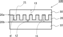
- FIG. 1 is a cross-sectional view illustrating an embodiment of an optical element according to the present disclosure.
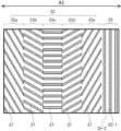
- FIG. 2 is a plan view illustrating one embodiment of a first surface of a patterned layer of an optical element of the present disclosure.
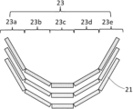
- FIG. 13 is a diagram for explaining ⁇ n.
- FIG. 13 is a diagram for explaining L1.
- FIG. 13 is a diagram for explaining D1 and D2.
- FIG. 13 is a plan view of one embodiment of a Y-shaped recess.
- FIG. 2 is a plan view showing an embodiment of a first surface of a pattern layer of an optical element corresponding to a comparative example.
- the optical element of the present disclosure comprises: An optical element having a pattern layer and a liquid crystal layer, the pattern layer has a first surface and a second surface opposite the first surface; the liquid crystal layer is formed on the first surface of the patterned layer; the patterned layer has a plurality of domains arranged in a first direction in the first plane; The domains form a domain unit consisting of a predetermined number of domains; Each of the domains has a plurality of recesses arranged in a second direction perpendicular to the first direction, Adjacent domains are in contact with each other, When an angle between an extension direction of the recess and the first direction in a domain located at an n-th position from one end of the domain unit in the first direction is defined as ⁇ n, ⁇ n changes stepwise from the one end to the other end of the domain unit in the first direction in a range from more than ⁇ 90.0 degrees to less than +90.0 degrees
- FIG. 1 is a cross-sectional view showing one embodiment of an optical element according to the present disclosure.
- the optical element 100 in Fig. 1 has a pattern layer 20 and a liquid crystal layer 30.
- the pattern layer 20 has a first surface 20a and a second surface 20b opposite to the first surface.
- the liquid crystal layer 30 is formed on the first surface 20a of the pattern layer 20.
- the pattern layer 20 has a plurality of recesses 21 on the first surface 20a.
- the optical element 100 in Fig. 1 has a substrate 10 on the side of the pattern layer 20 opposite to the liquid crystal layer 30.
- the reference character d indicates the depth of the recess.
- Fig. 1 indicates the depth of the recess.
- the reference character t1 indicates the thickness of the pattern layer at a portion that does not have a recess.
- the reference character t2 indicates the thickness of the pattern layer below the recess.
- the reference character t3 indicates the thickness of the liquid crystal layer formed at a portion that does not have a recess.
- Fig. 1 is a schematic cross-sectional view. That is, the scale of each layer constituting the optical element 100 and the scale of the recessed portion on the first surface are schematic for ease of illustration and differ from the actual scale. The same applies to other figures besides Fig. 1.
- the pattern layer has a first surface and a second surface opposite to the first surface.
- a liquid crystal layer is formed on the first surface of the pattern layer.
- a liquid crystal layer 30 is disposed within the recesses 21 of the patterned layer.
- the shape of the second surface 20b of the pattern layer is not particularly limited. In order to improve the adhesion between the second surface side of the pattern layer and other members such as a substrate, the second surface of the pattern layer is preferably flat.
- Configuration 1 The pattern layer has a plurality of domains arranged in a first direction within a first plane.
- Configuration 2 The domains form a domain unit consisting of a predetermined number of domains.
- Configuration 3 Each of the multiple domains has multiple recesses arranged in a second direction perpendicular to the first direction.
- a predetermined arrangement pattern of recesses can be formed from one end of the domain unit toward the other end. Furthermore, configurations 1 to 3 can easily prevent the individual recesses of the pattern layer from becoming too large, making it easier to form the pattern layer stably. By stabilizing the pattern layer, it is easier to align the liquid crystal molecules on the pattern layer, and the performance of the optical element can be stably exhibited.
- the smaller the individual recesses of the pattern layer the easier it is to peel the pattern layer from the shaping plate. Therefore, configurations 1 to 3 can easily form the pattern layer stably.
- the number of domain units may be only one, but it is preferable to have two or more domain units in the first direction.
- FIG. 2 is a plan view showing one embodiment of the first surface of the pattern layer.
- the pattern layer 20 has a plurality of domains arranged in the first direction A1 in the first surface.
- Reference numerals 23a to 23e are individual domains.
- the domains form a domain unit 23 in which a predetermined number of domains are assembled.
- FIG. 2 has one domain unit 23 in the first direction.
- the plurality of domains have a plurality of recesses 21 arranged in the second direction A2 perpendicular to the first direction A1 in each domain.
- adjacent domains are in contact with each other.
- domain 23a and domain 23b are in contact with each other.
- a boundary portion 25 is disposed at the end of the domain unit 23 in the first direction A1. It is preferable to have another domain unit (not shown) on the opposite side of the boundary portion 25 to the domain unit 23.
- Configuration 4 In the patterned layer, adjacent domains abut each other.
- the number of domains forming the domain unit is preferably 4 or more and 359 or less.
- the number of domains forming the domain unit 4 or more By making the number of domains forming the domain unit 4 or more, the angle of the recesses between adjacent domains can be suppressed from changing suddenly, so that the liquid crystal molecules can be easily aligned.
- the liquid crystal molecules can be easily aligned in the Y-shaped recesses described below.
- the number of domains forming the domain unit 359 or less the number of contact points of the recesses can be easily reduced, so that the liquid crystal molecules can be easily aligned.
- the number of domains forming the domain unit 359 or less the length of each recess in the extension direction can be easily increased, so that the liquid crystal molecules can be easily aligned.
- the number of domains constituting the domain unit is more preferably 6 or more and 200 or less, more preferably 10 or more and 100 or less, and even more preferably 15 or more and 50 or less.
- embodiments of the range of the number of domains that form the above domain unit include 4 to 359, 4 to 200, 4 to 100, 4 to 50, 6 to 359, 6 to 200, 6 to 100, 6 to 50, 10 to 359, 10 to 200, 10 to 100, 10 to 50, 15 to 359, 15 to 200, 15 to 100, and 15 to 50.
- the width of the domain can be adjusted appropriately depending on the purpose.
- the widths of the domains forming one domain unit may be the same or different.
- the width of the domain is the length of the domain in the first direction. As described above, the width of the domain is not particularly limited, but is usually 1.1 nm or more and 2000 ⁇ m or less.
- Configuration 5 When the angle between the extension direction of a recess and the first direction in a domain located at the nth position from one end of the domain unit in the first direction is defined as ⁇ n, ⁇ n changes stepwise from the one end to the other end of the domain unit in the first direction in a range from more than ⁇ 90.0 degrees to less than +90.0 degrees.
- the domain unit 23 is formed from multiple domains arranged in a first direction.
- "One end of the domain unit in the first direction" in configuration 5 means one end of the multiple domains arranged in the first direction. The ends exist on both sides, but either side may be used as the reference “one end.”
- Fig. 3 is a diagram for explaining ⁇ n.
- a domain unit 23 is formed by five domains 23a to 23e. Normally, each domain has a plurality of recesses 21, but in Fig. 3, for the sake of simplicity, only one recess is arranged in each domain.
- Fig. 3 is a diagram for explaining ⁇ n.
- a domain unit 23 is formed by five domains 23a to 23e. Normally, each domain has a plurality of recesses 21, but in Fig. 3, for the sake of simplicity, only one recess is arranged in each domain.
- the angle between the extension direction of the recess in the domain 23a and the first direction is ⁇ 1
- the angle between the extension direction of the recess in the domain 23b and the first direction is ⁇ 2
- the angle between the extension direction of the recess in the domain 23c and the first direction is ⁇ 3
- the angle between the extension direction of the recess in the domain 23d and the first direction is ⁇ 4
- the angle between the extension direction of the recess in the domain 23e and the first direction is ⁇ 5.
- ⁇ 3 is 0 degrees, so it is represented by a straight line. In Fig. 3, the angle changes stepwise from ⁇ 1 at one end to ⁇ 5 at the other end.
- Satisfying configuration 5 means that in one domain unit made up of multiple domains, the recesses are arranged in a semicircular or arc shape. Therefore, by satisfying configuration 5, the liquid crystal in the liquid crystal layer is also more likely to be oriented in a circular or arc shape along the arrangement of the recesses. And the liquid crystal layer arranged in a circular or arc shape has the effect of diffracting transmitted light.
- the absolute value is more preferably 0.9 degrees or more and 30.0 degrees or less, further preferably 1.8 degrees or more and 18.0 degrees or less, and further preferably 3.6 degrees or more and 12.0 degrees or less.
- measuring devices for the in-plane retardation include "AxoStep” manufactured by AXOMETRICS and a two-dimensional birefringence evaluation system (product name: WPA-Micro) manufactured by Photonic Lattice.
- the former product is suitable for measuring a wide area, and the latter product is suitable for measuring a narrow area.
- the diffraction angles in Table 1 are angles when there is one diffractive optical element. If the polarization state is the same, increasing the number of diffractive optical elements increases the diffraction angle as a multiplier of the number of diffractive optical elements. If the diffraction angle at an arbitrary pitch is ⁇ (degrees) and the number of diffractive optical elements is n, the diffraction angle can be expressed as 2 n-1 ⁇ (degrees).
- the present disclosure includes the following ⁇ 1> to ⁇ 11>.
- ⁇ 1> An optical element having a pattern layer and a liquid crystal layer, the pattern layer has a first surface and a second surface opposite the first surface; the liquid crystal layer is formed on the first surface of the patterned layer; the patterned layer has a plurality of domains arranged in a first direction in the first plane; The domains form a domain unit consisting of a predetermined number of domains; Each of the domains has a plurality of recesses arranged in a second direction perpendicular to the first direction, Adjacent domains are in contact with each other, When an angle between an extension direction of the recess and the first direction in a domain located at an n-th position from one end of the domain unit in the first direction is defined as ⁇ n, ⁇ n changes stepwise from the one end to the other end of the domain unit in the first direction in a range from more than ⁇ 90.0 degrees to less than +90.0 degrees, When the shortest distance between adjacent reces
- ⁇ 2> The optical element according to ⁇ 1>, wherein the number of the domains forming the domain unit is 4 or more and 359 or less.
- ⁇ 3> The optical element according to ⁇ 1> or ⁇ 2>, wherein, when a length in an extension direction of the recess in any domain is defined as L1, L1 in each domain becomes longer as an absolute value of ⁇ n of the domain increases.
- ⁇ 4> The optical element according to any one of ⁇ 1> to ⁇ 3>, wherein, when an angle between an extension direction of the recess and the first direction in a domain located at an n+1th position from one end of the domain unit in the first direction is defined as ⁇ n+1, an absolute value of a difference between ⁇ and ⁇ n+1 is 0.5 degrees or more and 36.0 degrees or less.
- the recesses include coupling recesses that contact the recesses of adjacent domains and non-coupling recesses that do not contact the recesses of adjacent domains.
- the coupling recesses include a double-sided coupling recess that contacts the recesses on both sides of adjacent domains on both sides, and a single-sided coupling recess that contacts the recesses on one side of adjacent domains on both sides.
- the coupling recess includes a coupling recess in which two recesses of one adjacent domain are coupled to one recess of the other adjacent domain.
- the liquid crystal layer has a single layer structure.
- ⁇ 9> The optical element according to any one of ⁇ 1> to ⁇ 7>, wherein the liquid crystal layer has a multi-layer structure.
- ⁇ 10> The optical element according to ⁇ 8>, wherein the liquid crystal layer has positive wavelength dispersion or negative wavelength dispersion.
- ⁇ 11> The optical element according to ⁇ 9>, wherein the liquid crystal layer has positive wavelength dispersion or negative wavelength dispersion.
- the releasability was evaluated according to the following criteria, and the results are shown in Table 3.
- D When forming the pattern layer, the shaping plate could not be peeled off from the shaped layer.
- the arrangement pattern of the recesses in the simulation shape used in the comparative example was a pattern in which the ends of the recesses in adjacent domains were all in contact with each other in the same manner in the second direction, as shown in Fig. 7.
- the arrangement pattern of the recesses in the simulation shape used in the examples was a pattern in which the degree of contact between the ends of the recesses in adjacent domains varied along the second direction.
- a quartz master mold with the surface shape designed by simulation was produced by an electron beam lithography process using an electron beam drawing device and a dry etching device.
- an ultraviolet-curable resin was poured into the mother mold, and then a transparent substrate was placed on the ultraviolet-curable resin.
- the resin was then cured by irradiating ultraviolet light.
- the transparent substrate and resin were then peeled off from the mother mold to obtain a resin plate having a shape complementary to that of the mother mold.
- a replica mold of the mother mold which is a mold having a shape complementary to that of the resin plate, was obtained by electroforming.
- a plurality of the replica molds were produced.
- a plurality of replica molds were wound around a roll to produce a roll-shaped plate to be used in the examples and comparative examples.
- a primer layer having the following formulation was applied onto a substrate (a cycloolefin polymer having a thickness of 40 ⁇ m; Zeonoa, a trade name of Zeon Corporation) and dried to form a primer layer having a thickness of 0.5 ⁇ m.
- a coating solution for forming a pattern layer having the following formulation was applied onto the primer layer and dried to form a layer containing an uncured resin.
- a layer containing uncured resin was shaped, and at the same time, ultraviolet light was irradiated from the substrate side (accumulated light amount: 500 mJ/ cm2 ) to cure the shaped layer containing resin.
- Example 1 an optical element of Example 1 was obtained.
- the optical element of Example 1 was produced by roll-to-roll production.
- ⁇ Coating liquid for forming primer layer> Polyolefin resin: 70 parts by mass (manufactured by Mitsubishi Chemical Corporation, product name: Surflen P-1000) Silica-based lubricant: 5 parts by mass (manufactured by CIK Nanotech, product name: SIRMIBK15WT%-E65) Methyl ethyl ketone: 25 parts by mass
- the optical elements of the examples have good alignment of the liquid crystal molecules, and therefore can fully demonstrate the performance of the optical elements.
- Substrate 20 Pattern layer 20a: First surface 20b: Second surface 21: Recess 22: Bonding recess 23: Domain units 23a, 23b, 23c, 23d, 23e, 23f, 23g, 23h: Individual domains 25: Boundary 25-1: Boundary recess 25-2: Convex 30: Liquid crystal layer 100: Optical element A1: First direction A2: Second direction
Landscapes
- Physics & Mathematics (AREA)
- General Physics & Mathematics (AREA)
- Optics & Photonics (AREA)
- Engineering & Computer Science (AREA)
- Manufacturing & Machinery (AREA)
- Liquid Crystal (AREA)
Priority Applications (3)
| Application Number | Priority Date | Filing Date | Title |
|---|---|---|---|
| CN202480057067.0A CN121794596A (zh) | 2023-09-11 | 2024-09-10 | 光学元件 |
| KR1020267007054A KR20260060332A (ko) | 2023-09-11 | 2024-09-10 | 광학 소자 |
| JP2025545689A JPWO2025057940A1 (cg-RX-API-DMAC7.html) | 2023-09-11 | 2024-09-10 |
Applications Claiming Priority (2)
| Application Number | Priority Date | Filing Date | Title |
|---|---|---|---|
| JP2023-146915 | 2023-09-11 | ||
| JP2023146915 | 2023-09-11 |
Publications (1)
| Publication Number | Publication Date |
|---|---|
| WO2025057940A1 true WO2025057940A1 (ja) | 2025-03-20 |
Family
ID=95021367
Family Applications (1)
| Application Number | Title | Priority Date | Filing Date |
|---|---|---|---|
| PCT/JP2024/032364 Ceased WO2025057940A1 (ja) | 2023-09-11 | 2024-09-10 | 光学素子 |
Country Status (5)
| Country | Link |
|---|---|
| JP (1) | JPWO2025057940A1 (cg-RX-API-DMAC7.html) |
| KR (1) | KR20260060332A (cg-RX-API-DMAC7.html) |
| CN (1) | CN121794596A (cg-RX-API-DMAC7.html) |
| TW (1) | TW202516255A (cg-RX-API-DMAC7.html) |
| WO (1) | WO2025057940A1 (cg-RX-API-DMAC7.html) |
Citations (4)
| Publication number | Priority date | Publication date | Assignee | Title |
|---|---|---|---|---|
| WO2019013320A1 (ja) * | 2017-07-14 | 2019-01-17 | 有限会社オートクローニングテクノロジー | 光学素子及び光回路 |
| JP2019536100A (ja) * | 2016-11-18 | 2019-12-12 | マジック リープ, インコーポレイテッドMagic Leap,Inc. | ナノスケールパターンを有する液晶回折デバイスおよびそれを製造するための方法 |
| WO2020004497A1 (ja) * | 2018-06-28 | 2020-01-02 | 富士フイルム株式会社 | 光学素子及び光学素子の製造方法 |
| JP2022075485A (ja) * | 2020-11-06 | 2022-05-18 | 株式会社ジャパンディスプレイ | 液晶光学素子 |
-
2024
- 2024-09-10 JP JP2025545689A patent/JPWO2025057940A1/ja active Pending
- 2024-09-10 CN CN202480057067.0A patent/CN121794596A/zh active Pending
- 2024-09-10 KR KR1020267007054A patent/KR20260060332A/ko active Pending
- 2024-09-10 WO PCT/JP2024/032364 patent/WO2025057940A1/ja not_active Ceased
- 2024-09-11 TW TW113134481A patent/TW202516255A/zh unknown
Patent Citations (4)
| Publication number | Priority date | Publication date | Assignee | Title |
|---|---|---|---|---|
| JP2019536100A (ja) * | 2016-11-18 | 2019-12-12 | マジック リープ, インコーポレイテッドMagic Leap,Inc. | ナノスケールパターンを有する液晶回折デバイスおよびそれを製造するための方法 |
| WO2019013320A1 (ja) * | 2017-07-14 | 2019-01-17 | 有限会社オートクローニングテクノロジー | 光学素子及び光回路 |
| WO2020004497A1 (ja) * | 2018-06-28 | 2020-01-02 | 富士フイルム株式会社 | 光学素子及び光学素子の製造方法 |
| JP2022075485A (ja) * | 2020-11-06 | 2022-05-18 | 株式会社ジャパンディスプレイ | 液晶光学素子 |
Also Published As
| Publication number | Publication date |
|---|---|
| KR20260060332A (ko) | 2026-05-04 |
| TW202516255A (zh) | 2025-04-16 |
| JPWO2025057940A1 (cg-RX-API-DMAC7.html) | 2025-03-20 |
| CN121794596A (zh) | 2026-04-03 |
Similar Documents
| Publication | Publication Date | Title |
|---|---|---|
| US11002955B2 (en) | Reverse-order crossed pancake lens with index gradient structure | |
| CN106371163B (zh) | 液晶固化膜、包含液晶固化膜的光学膜及显示装置 | |
| JP3592383B2 (ja) | 高分子製光学的ローパスフィルター、その複合体およびその製造方法並びに複合光学フィルター | |
| US11402696B2 (en) | Optical element and method of manufacturing optical element | |
| JP2020531905A (ja) | 回折導光板および回折導光板の製造方法 | |
| TW201643483A (zh) | 改善對比率的光學膜、包含該光學膜的偏光板以及包含上述的液晶顯示裝置 | |
| JP2020531908A (ja) | 回折導光板および回折導光板の製造方法 | |
| JP7533719B2 (ja) | 偏光板 | |
| TWI439761B (zh) | 液晶顯示器以及其中所使用的防眩光偏光膜疊層板 | |
| TWI746623B (zh) | 偏光消除元件 | |
| WO2025005173A1 (ja) | 光学素子 | |
| WO2017150697A1 (ja) | 表示体、および、表示体の観察方法 | |
| KR20260060332A (ko) | 광학 소자 | |
| JP2025087216A (ja) | 光学素子 | |
| JP2025176606A (ja) | 光学素子及び前記光学素子を含む装置 | |
| JP2025087217A (ja) | 光学素子 | |
| JP7666513B2 (ja) | 光学素子、及びその製造方法 | |
| JP2025102324A (ja) | 光学素子及び光学素子の検査方法 | |
| JP2014164142A (ja) | 配向基材と位相差フィルムとの積層体の製造方法、積層体、位相差フィルムおよび液晶表示装置 | |
| JP2023166849A (ja) | ビームステアリング素子及びこれを含むLiDAR | |
| JP2025103366A (ja) | 光学素子及び光学素子の製造方法 | |
| JP3134710B2 (ja) | 光学フィルム | |
| JP2025143672A (ja) | 光学素子、前記光学素子を含む装置、及び光学素子の製造方法 | |
| JP2017049392A (ja) | 光学フィルム用転写体、光学フィルム及び画像表示装置 | |
| JP2025012438A (ja) | 光学フィルム及び画像表示装置 |
Legal Events
| Date | Code | Title | Description |
|---|---|---|---|
| 121 | Ep: the epo has been informed by wipo that ep was designated in this application |
Ref document number: 24865440 Country of ref document: EP Kind code of ref document: A1 |
|
| ENP | Entry into the national phase |
Ref document number: 2025545689 Country of ref document: JP Kind code of ref document: A |
|
| WWE | Wipo information: entry into national phase |
Ref document number: 2025545689 Country of ref document: JP |
|
| NENP | Non-entry into the national phase |
Ref country code: DE |