WO2025057838A1 - アンテナ装置 - Google Patents
アンテナ装置 Download PDFInfo
- Publication number
- WO2025057838A1 WO2025057838A1 PCT/JP2024/031750 JP2024031750W WO2025057838A1 WO 2025057838 A1 WO2025057838 A1 WO 2025057838A1 JP 2024031750 W JP2024031750 W JP 2024031750W WO 2025057838 A1 WO2025057838 A1 WO 2025057838A1
- Authority
- WO
- WIPO (PCT)
- Prior art keywords
- dielectric layer
- radiation
- antenna device
- conductor wall
- electrode
- Prior art date
- Legal status (The legal status is an assumption and is not a legal conclusion. Google has not performed a legal analysis and makes no representation as to the accuracy of the status listed.)
- Pending
Links
Images






Classifications
-
- H—ELECTRICITY
- H01—ELECTRIC ELEMENTS
- H01Q—ANTENNAS, i.e. RADIO AERIALS
- H01Q13/00—Waveguide horns or mouths; Slot antennas; Leaky-waveguide antennas; Equivalent structures causing radiation along the transmission path of a guided wave
- H01Q13/08—Radiating ends of two-conductor microwave transmission lines, e.g. of coaxial lines, of microstrip lines
-
- H—ELECTRICITY
- H01—ELECTRIC ELEMENTS
- H01Q—ANTENNAS, i.e. RADIO AERIALS
- H01Q21/00—Antenna arrays or systems
- H01Q21/06—Arrays of individually energised antenna units similarly polarised and spaced apart
Definitions
- the present invention relates to an antenna device.
- Patent Document 1 and Patent Document 2 describe an antenna device that uses a high dielectric constant material as the dielectric layer.
- Patent Document 3 describes an antenna in which a conductor is provided on the outer periphery of a planar antenna and is connected to ground.
- JP 2006-60772 A Japanese Patent Application Publication No. 6-29723 JP 2020-43422 A
- Such antenna devices are required to be compact and have wideband antenna characteristics. Furthermore, the above-mentioned Patent Documents 1 to 3 do not take into consideration antenna devices that combine the respective configurations.
- the present invention aims to provide an antenna device that can be made compact and has broadband antenna characteristics.
- the antenna device includes a first dielectric layer, a radiation electrode provided on the first dielectric layer, a second dielectric layer having a higher relative dielectric constant than the first dielectric layer and covering the radiation electrode, a ground electrode facing the radiation electrode across the first dielectric layer and provided on the opposite side of the second dielectric layer, and a conductor wall extending along at least the thickness direction of the first dielectric layer of the first and second dielectric layers and provided along the outer edge of the radiation electrode in a planar view.
- the antenna device of the present invention can be made smaller and has broadband antenna characteristics.
- FIG. 1 is a perspective view showing an antenna device according to a first embodiment.
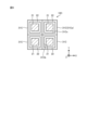
- FIG. 2 is a plan view showing a part of the antenna device according to the first embodiment.
- FIG. 3 is a cross-sectional view taken along line III-III' of FIG.
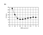
- FIG. 4 is a graph showing the relationship between the size of the ground electrode and the Q value of an antenna device according to a comparative example.
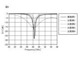
- FIG. 5 is a graph showing frequency characteristics of return loss for the antenna devices according to the first embodiment and the comparative example.
- FIG. 6 is a graph showing the relationship between the size of the ground electrode and the Q value of the antenna devices according to the first embodiment and the comparative example.
- FIG. 7 is a cross-sectional view showing an antenna device according to the second embodiment.
- FIG. 8 is a plan view showing an antenna device according to the third embodiment.
- FIG. 9 is a plan view showing an antenna device according to a first modified example of the third embodiment.
- FIG. 10 is a perspective view showing an antenna device according to the fourth embodiment.
- FIG. 11 is a cross-sectional view taken along line XI-XI' of FIG.
- FIG. 12 is a cross-sectional view showing a part of an antenna device according to a second modification of the fourth embodiment.
- FIG. 13 is a perspective view showing an antenna device according to a third modified example of the fourth embodiment.
- FIG. 14 is an explanatory diagram for explaining the polarization direction and the polar angle in the antenna apparatus according to the second to sixth embodiments.
- FIG. 15 is a graph showing a radiation pattern of the antenna device according to the second embodiment.
- FIG. 16 is a graph showing a radiation pattern of the antenna device according to the third embodiment.
- FIG. 17 is a graph showing a radiation pattern of the antenna device according to the fourth embodiment.
- FIG. 18 is a graph showing a radiation pattern of the antenna device according to the fifth embodiment.
- FIG. 19 is a graph showing a radiation pattern of the antenna device according to the sixth embodiment.
- FIG. 1 is a perspective view showing an antenna device according to a first embodiment.
- FIG. 2 is a plan view showing a part of the antenna device according to the first embodiment.
- FIG. 3 is a cross-sectional view taken along line III-III' in FIG. 2. Note that in FIG. 2, in order to make the drawing easier to see, the second dielectric layer 12 is omitted and the planar shapes of the electrodes and the conductor wall 31 are shown.
- the antenna device 10 has a first dielectric layer 11, a second dielectric layer 12, a radiation electrode 21, a ground electrode 22, and a conductor wall 31.
- the direction perpendicular to the surface of the radiation electrode 21 is defined as the Z direction
- the direction perpendicular to the Z direction is defined as the X direction
- the direction perpendicular to the Z direction and the X direction is defined as the Y direction.
- the X direction and the Y direction are both parallel to the surface of the radiation electrode 21.
- a plan view refers to the positional relationship when viewed from a direction perpendicular to the surface of the radiation electrode 21 (Z direction).
- the first dielectric layer 11 is a multi-layer substrate and has a rectangular shape in a plan view.
- the first dielectric layer 11 is flat and has a front surface 11a and a back surface 11b opposite the front surface 11a.
- the second dielectric layer 12 is laminated on the front surface 11a of the first dielectric layer 11.
- the second dielectric layer 12 has a higher relative dielectric constant than the first dielectric layer 11.
- the second dielectric layer 12 is a multi-layer substrate. However, the second dielectric layer 12 may be a single layer.
- the first dielectric layer 11 and the second dielectric layer 12 may be made of one or more of the following materials: low temperature co-fired ceramics (LTCC), glass epoxy resin, liquid crystal polymer (LCP), fluororesin, polyimide resin, etc.
- LTCC low temperature co-fired ceramics
- LCP liquid crystal polymer
- fluororesin polyimide resin
- polyimide resin etc.
- LTCC has the highest relative dielectric constant, followed by glass epoxy resin, liquid crystal polymer, and fluororesin in that order.
- the relative dielectric constant of the first dielectric layer 11 is about 2, and a fluororesin is used as the material for the first dielectric layer 11 with a low dielectric constant.
- the relative dielectric constant of the second dielectric layer 12 is about 7, and LTCC is used as the material for the second dielectric layer 12 with a high dielectric constant.
- the dielectric constants and materials of the first dielectric layer 11 and the second dielectric layer 12 are merely examples, and the combination of materials used for the first dielectric layer 11 and the second dielectric layer 12 can be changed as appropriate. By constructing the first dielectric layer 11 and the second dielectric layer 12 from different types of materials, the dielectric constant of the first dielectric layer 11 and the dielectric constant of the second dielectric layer 12 can be easily made different.
- the radiation electrode 21 is provided on the surface 11a of the first dielectric layer 11.
- the second dielectric layer 12 is provided to cover the radiation electrode 21. In other words, the radiation electrode 21 is located between the first dielectric layer 11 and the second dielectric layer 12 in the Z direction.
- the ground electrode 22 is provided on the back surface 11b of the first dielectric layer 11. That is, the ground electrode 22 faces the radiation electrode 21 across the first dielectric layer 11.
- the radiation electrode 21 and the ground electrode 22 form a patch antenna.
- the antenna device 10 is stacked in the Z direction in the order of the ground electrode 22, the first dielectric layer 11, the radiation electrode 21, and the second dielectric layer 12.
- a via 23 that penetrates the first dielectric layer 11 and a connection wiring 24 are connected to the power supply point of the radiation electrode 21.
- the connection wiring 24 is connected to an RFIC that is included in an external high-frequency circuit board. This causes a high-frequency signal to be supplied from the RFIC to the power supply point of the radiation electrode 21, and radio waves are emitted from the radiation electrode 21.
- the radiation electrode 21 and the ground electrode 22 are formed of a metal material having electrical conductivity.
- the radiation electrode 21 and the ground electrode 22 are formed of a metal material such as aluminum (Al), copper (Cu), gold (Au), silver (Ag), or an alloy containing at least one of these materials.
- the radiation electrode 21 and the ground electrode 22 are each rectangular in plan view.
- the electrode size of the ground electrode 22 is larger than the electrode size of the radiation electrode 21. That is, the width W2(x) of the ground electrode 22 in the X direction is larger than the width W1(x) of the radiation electrode 21 in the X direction. In addition, the width W2(y) of the ground electrode 22 in the Y direction is larger than the width W1(y) of the radiation electrode 21 in the Y direction.
- the width W2(x) can be said to be the length of each of the two sides of the ground electrode 22 that face each other in the Y direction.
- the width W2(y) can be said to be the length of each of the two sides of the ground electrode 22 that face each other in the X direction.
- At least one of the width W2(x) and width W2(y) of the ground electrode 22 is ⁇ or less. More preferably, at least one of the width W2(x) and width W2(y) of the ground electrode 22 is ⁇ /2 or less.
- the radiation electrode 21 and the ground electrode 22 are square, but are not limited to this.
- the radiation electrode 21 and the ground electrode 22 may be rectangular.
- the radiation electrode 21 and the ground electrode 22 are not limited to a square shape, and may be other shapes such as a polygonal shape or a circular shape.
- the conductor wall 31 is provided along the outer edge of the radiation electrode 21 in a plan view. More specifically, the conductor wall 31 extends along the four sides of the radiation electrode 21 and is formed into a rectangular frame surrounding the radiation electrode 21. As shown in FIG. 3, the conductor wall 31 extends along at least the thickness direction of the first dielectric layer 11 of the first dielectric layer 11 and the second dielectric layer 12. The height position of the upper end of the conductor wall 31 is substantially equal to the height position of the upper surface of the radiation electrode 21. In addition, the lower end side of the conductor wall 31 is connected to the ground electrode 22. A reference potential (e.g., ground potential) is supplied to the conductor wall 31 through the ground electrode 22.
- a reference potential e.g., ground potential
- the conductor wall 31 is formed of a metal material having electrical conductivity.
- the conductor wall 31 is made of the same material as the radiating electrode 21 and the ground electrode 22.
- the conductor wall 31 may be made of a different material than the radiating electrode 21 and the ground electrode 22.
- the conductor wall 31 is formed in the form of a film on the side surface of the first dielectric layer 11.
- the conductor wall 31 is formed by, for example, a sputtering method.
- the conductor wall 31 is formed by applying a metal paste. This allows the conductor wall 31 to be formed with a thinner thickness (the thickness of the conductor wall 31 in the X direction or the Y direction) compared to when the conductor wall 31 is formed using a via or the like that penetrates the first dielectric layer 11 in the Z direction, and the antenna device 10 can be made smaller. Alternatively, because the conductor wall 31 can be made thinner, the area of the radiation electrode 21 can be secured while the antenna device 10 is made smaller.
- the conductor walls 31 are provided opposite the side surfaces (four sides) of the radiation electrode 21, and the ground electrode 22 is provided opposite the lower surface of the radiation electrode 21.
- the upper surface of the radiation electrode 21 is covered with the second dielectric layer 12 formed of a high dielectric constant material. This allows the antenna device 10 to be miniaturized and have broadband radiation characteristics. The miniaturization (size of the ground electrode 22) and radiation characteristics of the antenna device 10 will be described with reference to Figures 4 to 6.
- the radiation electrode 21 is provided on the front surface 11a of the first dielectric layer 11, and the ground electrode 22 is provided on the back surface 11b of the first dielectric layer 11, but this is not limited to this.
- the radiation electrode 21 may be provided on an inner layer of the first dielectric layer 11.
- the ground electrode 22 may be provided on an inner layer of the first dielectric layer 11.
- the antenna device 10 is stacked in the Z direction in the following order: first dielectric layer 11, ground electrode 22, first dielectric layer 11, radiation electrode 21, first dielectric layer 11, and second dielectric layer 12.
- the conductor wall 31 is formed in a frame shape surrounding the four sides of the radiation electrode 21, but is not limited to this.
- the conductor wall 31 may be provided extending along at least two opposing sides of the four sides of the radiation electrode 21, and may not be provided on any one of the four sides of the radiation electrode 21.
- multiple conductor walls 31 may be arranged at a distance along the outer edge of the radiation electrode 21.
- Fig. 4 is a graph showing the relationship between the size of the ground electrode and the Q value of the antenna device according to the comparative example.
- Fig. 5 is a graph showing the frequency characteristics of the return loss of the antenna devices according to the example 1 and the comparative example.
- Fig. 6 is a graph showing the relationship between the size of the ground electrode and the Q value of the antenna devices according to the example 1 and the comparative example.
- the antenna device according to the comparative example shown in FIG. 4 is the antenna device 10 of the first embodiment, but does not have the second dielectric layer 12 and the conductor wall 31.
- the horizontal axis of the graph shown in FIG. 4 is the size of the ground electrode (the width W2(x) or W2(y) of the ground electrode 22 in FIG. 2), and the vertical axis is the Q value.
- the graph shown in FIG. 4 shows the results of simulating the Q value of the radiation characteristics under conditions of a frequency of 28 GHz and a substrate dielectric constant of 3.
- the Q value is roughly constant.
- the width of the ground electrode is 3.5 mm or less (approximately ⁇ /2 or less in electrical length)
- the Q value tends to increase. In other words, when the electrode size of the ground electrode becomes small, it may become difficult to achieve a wideband radiation characteristic.
- the antenna device according to the embodiment shown in Figures 5 and 6 has a similar configuration to the antenna device 10 of the first embodiment, with the first dielectric layer 11 having a relative dielectric constant of 3 and a thickness of 0.4 mm.
- the second dielectric layer 12 has a relative dielectric constant of 6 and a thickness of 0.8 mm.
- the widths W2(x) and W2(y) of the ground electrode 22 are each 3.0 mm.
- Comparative examples 1 and 2 are configured without the second dielectric layer 12 and conductor wall 31 compared to the antenna device of Example 1.
- Comparative examples 3 and 4 are configured without the conductor wall 31 compared to the antenna device of Example 1, but have the same configuration as the antenna device of Example 1, in that they have the second dielectric layer 12.
- the width of the ground electrode in Comparative examples 1 and 3 is 7.5 mm
- the width of the ground electrode in Comparative examples 2 and 4 is 3.0 mm.
- Comparative examples 1 and 2 are the same as some of the comparative examples shown in Figure 4 above (with ground electrode widths of 7.5 mm and 3.0 mm).
- Figures 5 and 6 show the results of simulating the return loss and Q value for the embodiment and comparative examples 1 to 4.
- the horizontal axis of the graph shown in Figure 5 is frequency (GHz), and the vertical axis is the level (dB) of the S parameter S11.
- the horizontal axis of the graph shown in Figure 6 is the width (mm) of the ground electrode, and the vertical axis is the Q value.
- Comparative Examples 3 and 4 have a smaller Q value than Comparative Examples 1 and 2 because they have a second dielectric layer made of a high dielectric constant material. That is, Comparative Examples 3 and 4 have a broader band radiation characteristic than Comparative Examples 1 and 2. Comparative Examples 2 and 4 (3.0 mm) in which the ground electrode is small in width have a larger Q value than Comparative Examples 1 and 3 (7.5 mm) in which the ground electrode is large in width.
- Comparative Examples 2 and 4 (3.0 mm) in which the ground electrode is small in width
- the Q value of Comparative Example 4 which is provided with a second dielectric layer made of a high dielectric constant material, has a smaller Q value suppression effect than Comparative Example 2, which does not have a second dielectric layer. That is, when the antenna device is made smaller in size, the effect of improving the radiation characteristic is small just by providing a second dielectric layer.
- the antenna device according to the embodiment is provided with a second dielectric layer 12 made of a high dielectric constant material and a conductor wall 31, which shows that the Q value can be reduced compared to Comparative Examples 2 and 4 even when the width of the ground electrode is small (3.0 mm).
- the antenna device according to the embodiment can be miniaturized and has a wide band of radiation characteristics.
- Example 1 the relative dielectric constants and ground electrode widths shown in Example 1 and each comparative example are merely examples and are not limited to these.
- Second Embodiment Fig. 7 is a cross-sectional view showing an antenna device according to a second embodiment.
- the antenna device 10A according to the second embodiment is different from the first embodiment in that it has a first radiation electrode 25 and a second radiation electrode 26 as radiation electrodes.
- the antenna device 10A according to the second embodiment is different from the first embodiment in that the conductor wall 31A is formed inside the first dielectric layer 11, i.e., on the inner side of the side surface of the first dielectric layer 11.
- the first radiation electrode 25 is a patch electrode for the high frequency side
- the second radiation electrode 26 is a patch electrode for the low frequency side. That is, the first radiation electrode 25 is electrically connected to an external RFIC (not shown) through a via 27.
- the second radiation electrode 26 is electrically connected to an external RFIC (not shown) through a via 28.
- the first radiation electrode 25 and the second radiation electrode 26 are configured to receive different high frequency signals from the external RFIC (not shown) and to emit radio waves in different frequency bands.
- the antenna device 10A of this embodiment can operate in multiple frequency bands, and can achieve broadband radiation characteristics in each frequency band, just like the first embodiment described above.
- the conductor wall 31A of this embodiment can be formed in the same process as the process for forming the first radiation electrode 25, the second radiation electrode 26, the vias 27, 28, etc. Therefore, in this embodiment, the conductor wall 31A can be easily formed. Furthermore, since the conductor wall 31A has a greater degree of freedom in placement compared to the conductor wall 31 of the first embodiment, it can be placed between adjacent radiation electrodes even when configured as an array antenna.
- the length of each of the two sides of the ground electrode 22 that face each other in the X direction and extend in the Y direction is ⁇ or less. More preferably, the length of each of the two sides of the ground electrode 22 that face each other in the X direction and extend in the Y direction is ⁇ /2 or less.
- the antenna device 10A can obtain wideband radiation characteristics even when configured as an array antenna with a narrow width in the Y direction.
- Third Embodiment Fig. 8 is a plan view showing an antenna device according to a third embodiment.
- the antenna device 10B according to the third embodiment is different from the above-mentioned embodiments in that it is an array antenna in which a plurality of radiation electrodes 21 are arranged in the X direction.
- the multiple radiation electrodes 21 are provided on a common first dielectric layer 11.
- the second dielectric layer 12 is provided to cover the multiple radiation electrodes 21.
- the first dielectric layer 11 and the second dielectric layer 12 are provided continuously across the multiple radiation electrodes 21.
- the ground electrode 22 is formed as a common electrode for the multiple radiation electrodes 21.
- the conductor wall 31B is provided surrounding each of the multiple radiation electrodes 21.
- the conductor wall 31B can be a combination of the conductor wall 31 of the first embodiment and the conductor wall 31A of the second embodiment. That is, of the conductor walls 31B, the conductor wall 31Ba located on the outer periphery of the multiple radiation electrodes 21 is composed of a conductor film covering the side surface of the first dielectric layer 11, similar to the conductor wall 31 of the first embodiment. Also, of the conductor walls 31B, the conductor wall 31Bb located between the multiple radiation electrodes 21 adjacent to each other in the X direction is composed of multiple vias 33 and multiple connection pads 34 connected together, similar to the conductor wall 31A of the second embodiment.
- the thickness of the conductor wall 31Ba located on the outer periphery can be made thinner than the conductor wall 31Bb, making it possible to miniaturize the antenna device 10B.
- the conductor wall 31B is provided on each of the multiple radiation electrodes 21, it is possible to achieve a broadband radiation characteristic in the array antenna as in the first embodiment described above.
- FIG. 9 is a plan view showing an antenna device according to a first modified example of the third embodiment.
- an antenna device 10C according to the first modified example of the third embodiment differs from the third embodiment in that a plurality of radiation electrodes 21 are arranged in the X direction and are an array antenna arranged in the Y direction.
- the antenna device 10C is configured as a two-dimensional array antenna.
- the conductor walls 31C are provided to surround each of the multiple radiation electrodes 21.
- the conductor walls 31Ca of the conductor walls 31C located on the outer periphery of the multiple radiation electrodes 21 are made of a conductor film covering the side surface of the first dielectric layer 11, similar to the conductor walls 31 of the first embodiment.
- the conductor walls 31Cb of the conductor walls 31C located between the multiple radiation electrodes 21 adjacent in the X direction and the conductor walls 31Cc located between the multiple radiation electrodes 21 adjacent in the Y direction are made by connecting multiple vias 33 and multiple connection pads 34, similar to the conductor walls 31A of the second embodiment.
- Fig. 10 is a perspective view showing an antenna device according to a fourth embodiment.
- Fig. 11 is a cross-sectional view taken along the line XI-XI' of Fig. 10.
- Fig. 11 shows a cross-sectional view of a part of the antenna device 10D, that is, a part of the antenna device 10D corresponding to one first radiation electrode 25 and one of the plurality of second radiation electrodes 26 among the plurality of first radiation electrodes 25 and the plurality of second radiation electrodes 26.
- the antenna device 10D according to the fourth embodiment differs from the above-described embodiment and modified example in that the conductor wall 31D includes a first conductor wall 35 and a second conductor wall 36.
- the antenna device 10D of this embodiment has a plurality of first radiation electrodes 25 and a plurality of second radiation electrodes 26, which are arranged in the X direction.
- the configurations of the first radiation electrodes 25, the second radiation electrodes 26, the first dielectric layer 11, and the second dielectric layer 12 are similar to those of the second embodiment described above (see FIG. 7), and a repeated description will be omitted.
- the first conductor wall 35 is provided on the first dielectric layer 11 and is provided along the thickness direction (Z direction) of the first dielectric layer 11. In this embodiment, the height of the first conductor wall 35 is equal to the thickness of the first dielectric layer 11. Furthermore, the multiple first conductor walls 35 each extend along the Y direction and are arranged in the X direction. The first conductor wall 35 is disposed between the multiple first radiation electrodes 25 adjacent to each other in the X direction and the multiple second radiation electrodes 26 adjacent to each other in the X direction.
- the second dielectric layer 12 is provided to cover the first radiation electrode 25, the second radiation electrode 26, the first dielectric layer 11, and the first conductor wall 35.
- the second conductor wall 36 is provided on the second dielectric layer 12, overlapping the first conductor wall 35.
- the second dielectric layer 12 is arranged between the first conductor wall 35 and the second conductor wall 36 in the Z direction.
- the second conductor wall 36 is provided apart from the first conductor wall 35 and in a non-contact state.
- the multiple second conductor walls 36 overlap the first conductor wall 35 and extend in the same direction as the first conductor wall 35.
- the multiple second conductor walls 36 each extend along the Y direction and are arranged in the X direction.
- the second conductor walls 36 are arranged between the multiple first radiation electrodes 25 adjacent to each other in the X direction and between the multiple second radiation electrodes 26 adjacent to each other in the X direction.
- the conductor wall 31D (first conductor wall 35 and second conductor wall 36) does not have a portion extending in the X direction. That is, the conductor wall 31D is provided along two of the four sides of each of the first radiation electrode 25 and the second radiation electrode 26 that face in the X direction. Furthermore, the conductor wall 31D is not provided along two of the four sides of each of the first radiation electrode 25 and the second radiation electrode 26 that face in the Y direction.
- the first conductor wall 35 and the second conductor wall 36 are formed of a metal material having electrical conductivity.
- the first conductor wall 35 and the second conductor wall 36 are formed of a metal material such as aluminum (Al) or copper (Cu), or an alloy containing at least one of these materials.
- the lower end side of the first conductor wall 35 is connected to the ground electrode 22 and is supplied with a reference potential (e.g., ground potential).
- a reference potential e.g., ground potential
- the second conductor wall 36 is not in contact with the first conductor wall 35.
- the second conductor wall 36 may be connected to the reference potential at any point, or may be floating, in which case a fixed potential such as a reference potential is not supplied.
- the first conductor wall 35 and the second conductor wall 36 are provided, so that the current flowing on the second dielectric layer 12 is suppressed, and good radiation characteristics can be obtained.
- the radiation characteristics of the antenna device 10D will be described later with reference to Figures 15 to 19.
- FIG. 12 is a cross-sectional view showing a part of an antenna device according to a second modification of the fourth embodiment. As shown in Fig. 12, the antenna device 10E according to the second modification is different from the antenna device 10D according to the fourth embodiment in that the second conductor wall 36 of the conductor wall 31E is in contact with the first conductor wall 35.
- the antenna device 10E according to the second modified example can suppress the current flowing on the second dielectric layer 12, as in the fourth embodiment, and can obtain good radiation characteristics.
- FIG. 13 is a perspective view showing an antenna device according to a third modified example of the fourth embodiment.
- an antenna device 10F according to the third modified example is different from the fourth embodiment described above in that a second conductor wall 36A of a conductor wall 31F has a ladder shape.
- the conductor wall 31F includes a first conductor wall 35A and a second conductor wall 36A.
- the first conductor wall 35A is similar to the first conductor wall 35 described in the fourth embodiment, and a repeated description will be omitted.
- the second conductor wall 36A has a plurality of first portions 36Aa and a plurality of second portions 36Ab.
- the plurality of first portions 36Aa are provided so as to overlap with the plurality of first conductor walls 35A, respectively. That is, the plurality of first portions 36Aa each extend in the Y direction and are arranged in the X direction.
- the multiple second portions 36Ab each extend in the X direction and are arranged at intervals in the Y direction.
- One end side of the multiple first portions 36Aa is connected to one of the second portions 36Ab, and the other end side of the multiple first portions 36Aa is connected to the other of the second portions 36Ab.
- the first radiation electrode 25 and the second radiation electrode 26 are arranged in the area defined by the two first portions 36Aa and the two second portions 36Ab.
- the second conductor wall 36A and the first conductor wall 35A are stacked without contact with each other with the second dielectric layer 12 sandwiched therebetween, as in the fourth embodiment.
- the second conductor wall 36A and the first conductor wall 35A may be stacked in direct contact with each other, as in the second modified example (see FIG. 12).
- the configuration is not limited to one in which a plurality of first conductor walls 35A are arranged in the X direction, and the first conductor wall 35A may also be formed in a ladder shape, similar to the second conductor wall 36A.
- the first conductor wall 35A may be provided surrounding each of the plurality of first radiation electrodes 25 and the plurality of second radiation electrodes 26.
- Fig. 14 is an explanatory diagram for explaining the polarization direction and polar angle in the antenna devices according to Examples 2 to 6.
- Fig. 15 is a graph showing the radiation pattern of the antenna device according to Example 2.
- Fig. 16 is a graph showing the radiation pattern of the antenna device according to Example 3.
- Fig. 17 is a graph showing the radiation pattern of the antenna device according to Example 4.
- Fig. 18 is a graph showing the radiation pattern of the antenna device according to Example 5.
- Fig. 19 is a graph showing the radiation pattern of the antenna device according to Example 6.
- FIG. 14 illustrates the antenna device 10D according to the fourth embodiment
- the explanation of the polarization direction and polar angle of the antenna device 10D can be applied to any of Examples 2 to 6.
- the polarized waves in the Y direction are represented as vertical polarization V-pol
- the polarized waves in the X direction are represented as horizontal polarization H-pol.
- the angle of the direction tilted in the X direction with respect to the direction perpendicular to the surfaces of the first radiation electrode 25 and the second radiation electrode 26 (Z direction) is represented as the polar angle ⁇ (x) in the X direction.
- the angle of the direction tilted in the Y direction with respect to the direction perpendicular to the surfaces of the first radiation electrode 25 and the second radiation electrode 26 (Z direction) is represented as the polar angle ⁇ (y) in the Y direction.
- the antenna device according to Example 2 shown in FIG. 15 is the antenna device 10D of the fourth embodiment (see FIG. 10 and FIG. 11) without the second conductor wall 36.
- the antenna device according to Example 3 shown in FIG. 16 is the same as the antenna device 10D of the fourth embodiment (see FIG. 10 and FIG. 11).
- the antenna device according to Example 4 shown in FIG. 17 is the same as the antenna device 10F of the third modified example (see FIG. 13).
- the antenna device according to Example 5 shown in FIG. 18 is the same as the antenna device 10E of the second modified example (see FIG. 12).
- the antenna device according to Example 6 shown in FIG. 19 is the antenna device 10F of the third modified example (see FIG. 13) with the second conductor wall 36A and the first conductor wall 35A stacked in direct contact with each other.
- Graphs shown in Figures 15 to 19 show the results of simulating the radiation patterns for the antenna devices according to Examples 2 to 6.
- the horizontal axis of each graph is the polar angle (deg.).
- the vertical axis of each graph is the gain (dB).
- the radiation pattern of vertically polarized wave V-pol (upper row) and the radiation pattern of horizontally polarized wave H-pol (lower row) are shown.
- radiation patterns of different frequency bands (Low band (left side), High band (right side)) are shown.
- the high frequency band (High band) corresponds to the radiation pattern by the first radiation electrode 25
- the low-high frequency band (Low band) corresponds to the radiation pattern by the second radiation electrode 26.
- the antenna devices according to Examples 3 to 6 having the second conductor walls 36, 36A have smoother radiation patterns when the polar angle in the X direction is changed, compared to Example 2 not having the second conductor walls 36, 36A. In other words, it was shown that Examples 3 to 6 suppress the variation in gain when the polar angle in the X direction is changed, compared to Example 2.
- the antenna gain at a polar angle of 0° (Z direction) is greater than in Example 2, at least in the radiation pattern of the high frequency band (High band).
- this disclosure can also have the following configurations.
- a first dielectric layer a radiation electrode provided on the first dielectric layer; a second dielectric layer having a higher dielectric constant than the first dielectric layer and covering the radiation electrode; a ground electrode disposed opposite the radiation electrode with the first dielectric layer therebetween and opposite the second dielectric layer; a conductor wall extending along a thickness direction of at least the first dielectric layer of the first and second dielectric layers and provided along an outer edge of the radiation electrode in a plan view.
- the radiation electrode is A first radiation electrode;
- a plurality of the radiation electrodes are provided, The plurality of radiation electrodes are arranged in a first direction parallel to a surface of the first dielectric layer, The antenna device according to any one of (1) to (4), wherein the conductive wall is provided to surround each of the plurality of radiation electrodes.
- the antenna device (6) The antenna device according to (5), wherein the plurality of radiation electrodes are arranged in the first direction and also in a second direction perpendicular to the first direction. (7) The antenna device described in any one of (1) to (6), wherein the conductor wall includes a plurality of vias arranged in a thickness direction of the first dielectric layer and a plurality of connection pads connecting the plurality of vias arranged in the thickness direction. (8) The antenna device according to any one of (1) to (6), wherein the conductor wall is provided in the form of a film on at least a side surface of the first dielectric layer.
- the conductive wall includes a first conductive wall provided on the first dielectric layer and a second conductive wall provided to overlap the first conductive wall, The antenna device according to any one of (1) to (8), wherein the second dielectric layer is disposed between the first conductive wall and the second conductive wall.
- the conductive wall includes a first conductive wall provided on the first dielectric layer and a second conductive wall provided to overlap the first conductive wall, The antenna device according to any one of (1) to (8), wherein the first conductive wall and the second conductive wall are provided in direct contact with each other.
- a microwave oven having a plurality of the radiation electrodes, The plurality of radiation electrodes are arranged in a first direction
- the antenna device according to (9) or (10) wherein the first conductor wall and the second conductor wall extend in a second direction perpendicular to the first direction and are disposed between a plurality of the radiation electrodes arranged in the first direction in a planar view.
- the ground electrode includes at least two opposing sides, The antenna device according to any one of (1) to (12), wherein each of the two opposing sides has a length of ⁇ or less.
- the ground electrode includes at least two opposing sides, The antenna device according to any one of (1) to (12), wherein each of the two opposing sides has a length of ⁇ /2 or less.
Landscapes
- Details Of Aerials (AREA)
Priority Applications (1)
| Application Number | Priority Date | Filing Date | Title |
|---|---|---|---|
| JP2025545636A JPWO2025057838A1 (https=) | 2023-09-13 | 2024-09-04 |
Applications Claiming Priority (2)
| Application Number | Priority Date | Filing Date | Title |
|---|---|---|---|
| JP2023-148721 | 2023-09-13 | ||
| JP2023148721 | 2023-09-13 |
Publications (1)
| Publication Number | Publication Date |
|---|---|
| WO2025057838A1 true WO2025057838A1 (ja) | 2025-03-20 |
Family
ID=95021207
Family Applications (1)
| Application Number | Title | Priority Date | Filing Date |
|---|---|---|---|
| PCT/JP2024/031750 Pending WO2025057838A1 (ja) | 2023-09-13 | 2024-09-04 | アンテナ装置 |
Country Status (2)
| Country | Link |
|---|---|
| JP (1) | JPWO2025057838A1 (https=) |
| WO (1) | WO2025057838A1 (https=) |
Citations (4)
| Publication number | Priority date | Publication date | Assignee | Title |
|---|---|---|---|---|
| JPH03173203A (ja) * | 1989-12-01 | 1991-07-26 | Murata Mfg Co Ltd | マイクロストリップアンテナ |
| WO2019054094A1 (ja) * | 2017-09-12 | 2019-03-21 | 株式会社村田製作所 | アンテナモジュール |
| WO2022185874A1 (ja) * | 2021-03-02 | 2022-09-09 | 株式会社村田製作所 | アンテナモジュールおよびそれを搭載した通信装置 |
| WO2023047801A1 (ja) * | 2021-09-22 | 2023-03-30 | 株式会社村田製作所 | アンテナモジュールおよびそれを搭載する通信装置 |
-
2024
- 2024-09-04 JP JP2025545636A patent/JPWO2025057838A1/ja active Pending
- 2024-09-04 WO PCT/JP2024/031750 patent/WO2025057838A1/ja active Pending
Patent Citations (4)
| Publication number | Priority date | Publication date | Assignee | Title |
|---|---|---|---|---|
| JPH03173203A (ja) * | 1989-12-01 | 1991-07-26 | Murata Mfg Co Ltd | マイクロストリップアンテナ |
| WO2019054094A1 (ja) * | 2017-09-12 | 2019-03-21 | 株式会社村田製作所 | アンテナモジュール |
| WO2022185874A1 (ja) * | 2021-03-02 | 2022-09-09 | 株式会社村田製作所 | アンテナモジュールおよびそれを搭載した通信装置 |
| WO2023047801A1 (ja) * | 2021-09-22 | 2023-03-30 | 株式会社村田製作所 | アンテナモジュールおよびそれを搭載する通信装置 |
Also Published As
| Publication number | Publication date |
|---|---|
| JPWO2025057838A1 (https=) | 2025-03-20 |
Similar Documents
| Publication | Publication Date | Title |
|---|---|---|
| US9698487B2 (en) | Array antenna | |
| US11171421B2 (en) | Antenna module and communication device equipped with the same | |
| EP1515389B1 (en) | Multilayer high frequency device with planar antenna thereon and manufacturing method thereof | |
| US9172142B2 (en) | Horizontal radiation antenna | |
| KR20210050452A (ko) | 안테나 구조체, 이를 포함하는 안테나 어레이 및 디스플레이 장치 | |
| US20150351222A1 (en) | Resin multilayer substrate and electronic apparatus | |
| US20100231320A1 (en) | Semiconductor device, transmission system, method for manufacturing semiconductor device, and method for manufacturing transmission system | |
| TW201842712A (zh) | 高頻模組 | |
| WO2012081288A1 (ja) | 高周波用パッケージ | |
| JP7047910B2 (ja) | アンテナ装置 | |
| US12120812B2 (en) | Circuit board and method of manufacturing thereof | |
| JP2024050679A (ja) | 配線基体および電子装置 | |
| US20230135990A1 (en) | Antenna device | |
| JP7315043B2 (ja) | パッチアンテナ | |
| US20220224006A1 (en) | Antenna device | |
| JP7435751B2 (ja) | 多層基板 | |
| WO2025057838A1 (ja) | アンテナ装置 | |
| US20240291166A1 (en) | Antenna module and communication apparatus including the same | |
| US11984637B2 (en) | Transmission line and electronic device | |
| US12062842B2 (en) | Antenna element and electronic device | |
| JP3071761B2 (ja) | 高周波用半導体装置の実装構造 | |
| TWI848584B (zh) | 毫米波埋入式天線 | |
| US20250226582A1 (en) | Antenna module | |
| WO2025234181A1 (ja) | アンテナ及び電子機器 | |
| JP2022034605A (ja) | 複合基板 |
Legal Events
| Date | Code | Title | Description |
|---|---|---|---|
| 121 | Ep: the epo has been informed by wipo that ep was designated in this application |
Ref document number: 24865339 Country of ref document: EP Kind code of ref document: A1 |
|
| ENP | Entry into the national phase |
Ref document number: 2025545636 Country of ref document: JP Kind code of ref document: A |
|
| WWE | Wipo information: entry into national phase |
Ref document number: 2025545636 Country of ref document: JP |