WO2025057569A1 - 絶縁ゲート型半導体装置 - Google Patents
絶縁ゲート型半導体装置 Download PDFInfo
- Publication number
- WO2025057569A1 WO2025057569A1 PCT/JP2024/026284 JP2024026284W WO2025057569A1 WO 2025057569 A1 WO2025057569 A1 WO 2025057569A1 JP 2024026284 W JP2024026284 W JP 2024026284W WO 2025057569 A1 WO2025057569 A1 WO 2025057569A1
- Authority
- WO
- WIPO (PCT)
- Prior art keywords
- contact
- semiconductor device
- trench
- region
- dummy
- Prior art date
- Legal status (The legal status is an assumption and is not a legal conclusion. Google has not performed a legal analysis and makes no representation as to the accuracy of the status listed.)
- Ceased
Links
Images







Classifications
-
- H—ELECTRICITY
- H10—SEMICONDUCTOR DEVICES; ELECTRIC SOLID-STATE DEVICES NOT OTHERWISE PROVIDED FOR
- H10D—INORGANIC ELECTRIC SEMICONDUCTOR DEVICES
- H10D12/00—Bipolar devices controlled by the field effect, e.g. insulated-gate bipolar transistors [IGBT]
- H10D12/411—Insulated-gate bipolar transistors [IGBT]
- H10D12/441—Vertical IGBTs
- H10D12/461—Vertical IGBTs having non-planar surfaces, e.g. having trenches, recesses or pillars in the surfaces of the emitter, base or collector regions
- H10D12/481—Vertical IGBTs having non-planar surfaces, e.g. having trenches, recesses or pillars in the surfaces of the emitter, base or collector regions having gate structures on slanted surfaces, on vertical surfaces, or in grooves, e.g. trench gate IGBTs
-
- H—ELECTRICITY
- H10—SEMICONDUCTOR DEVICES; ELECTRIC SOLID-STATE DEVICES NOT OTHERWISE PROVIDED FOR
- H10D—INORGANIC ELECTRIC SEMICONDUCTOR DEVICES
- H10D30/00—Field-effect transistors [FET]
- H10D30/01—Manufacture or treatment
- H10D30/021—Manufacture or treatment of FETs having insulated gates [IGFET]
- H10D30/028—Manufacture or treatment of FETs having insulated gates [IGFET] of double-diffused metal oxide semiconductor [DMOS] FETs
- H10D30/0291—Manufacture or treatment of FETs having insulated gates [IGFET] of double-diffused metal oxide semiconductor [DMOS] FETs of vertical DMOS [VDMOS] FETs
- H10D30/0295—Manufacture or treatment of FETs having insulated gates [IGFET] of double-diffused metal oxide semiconductor [DMOS] FETs of vertical DMOS [VDMOS] FETs using recessing of the source electrodes
-
- H—ELECTRICITY
- H10—SEMICONDUCTOR DEVICES; ELECTRIC SOLID-STATE DEVICES NOT OTHERWISE PROVIDED FOR
- H10D—INORGANIC ELECTRIC SEMICONDUCTOR DEVICES
- H10D30/00—Field-effect transistors [FET]
- H10D30/01—Manufacture or treatment
- H10D30/021—Manufacture or treatment of FETs having insulated gates [IGFET]
- H10D30/028—Manufacture or treatment of FETs having insulated gates [IGFET] of double-diffused metal oxide semiconductor [DMOS] FETs
- H10D30/0291—Manufacture or treatment of FETs having insulated gates [IGFET] of double-diffused metal oxide semiconductor [DMOS] FETs of vertical DMOS [VDMOS] FETs
- H10D30/0297—Manufacture or treatment of FETs having insulated gates [IGFET] of double-diffused metal oxide semiconductor [DMOS] FETs of vertical DMOS [VDMOS] FETs using recessing of the gate electrodes, e.g. to form trench gate electrodes
-
- H—ELECTRICITY
- H10—SEMICONDUCTOR DEVICES; ELECTRIC SOLID-STATE DEVICES NOT OTHERWISE PROVIDED FOR
- H10D—INORGANIC ELECTRIC SEMICONDUCTOR DEVICES
- H10D30/00—Field-effect transistors [FET]
- H10D30/60—Insulated-gate field-effect transistors [IGFET]
- H10D30/64—Double-diffused metal-oxide semiconductor [DMOS] FETs
- H10D30/66—Vertical DMOS [VDMOS] FETs
- H10D30/668—Vertical DMOS [VDMOS] FETs having trench gate electrodes, e.g. UMOS transistors
-
- H—ELECTRICITY
- H10—SEMICONDUCTOR DEVICES; ELECTRIC SOLID-STATE DEVICES NOT OTHERWISE PROVIDED FOR
- H10D—INORGANIC ELECTRIC SEMICONDUCTOR DEVICES
- H10D62/00—Semiconductor bodies, or regions thereof, of devices having potential barriers
- H10D62/10—Shapes, relative sizes or dispositions of the regions of the semiconductor bodies; Shapes of the semiconductor bodies
- H10D62/102—Constructional design considerations for preventing surface leakage or controlling electric field concentration
- H10D62/103—Constructional design considerations for preventing surface leakage or controlling electric field concentration for increasing or controlling the breakdown voltage of reverse-biased devices
-
- H—ELECTRICITY
- H10—SEMICONDUCTOR DEVICES; ELECTRIC SOLID-STATE DEVICES NOT OTHERWISE PROVIDED FOR
- H10D—INORGANIC ELECTRIC SEMICONDUCTOR DEVICES
- H10D62/00—Semiconductor bodies, or regions thereof, of devices having potential barriers
- H10D62/10—Shapes, relative sizes or dispositions of the regions of the semiconductor bodies; Shapes of the semiconductor bodies
- H10D62/124—Shapes, relative sizes or dispositions of the regions of semiconductor bodies or of junctions between the regions
- H10D62/126—Top-view geometrical layouts of the regions or the junctions
-
- H—ELECTRICITY
- H10—SEMICONDUCTOR DEVICES; ELECTRIC SOLID-STATE DEVICES NOT OTHERWISE PROVIDED FOR
- H10D—INORGANIC ELECTRIC SEMICONDUCTOR DEVICES
- H10D62/00—Semiconductor bodies, or regions thereof, of devices having potential barriers
- H10D62/10—Shapes, relative sizes or dispositions of the regions of the semiconductor bodies; Shapes of the semiconductor bodies
- H10D62/124—Shapes, relative sizes or dispositions of the regions of semiconductor bodies or of junctions between the regions
- H10D62/126—Top-view geometrical layouts of the regions or the junctions
- H10D62/127—Top-view geometrical layouts of the regions or the junctions of cellular field-effect devices, e.g. multicellular DMOS transistors or IGBTs
-
- H—ELECTRICITY
- H10—SEMICONDUCTOR DEVICES; ELECTRIC SOLID-STATE DEVICES NOT OTHERWISE PROVIDED FOR
- H10D—INORGANIC ELECTRIC SEMICONDUCTOR DEVICES
- H10D62/00—Semiconductor bodies, or regions thereof, of devices having potential barriers
- H10D62/60—Impurity distributions or concentrations
-
- H—ELECTRICITY
- H10—SEMICONDUCTOR DEVICES; ELECTRIC SOLID-STATE DEVICES NOT OTHERWISE PROVIDED FOR
- H10D—INORGANIC ELECTRIC SEMICONDUCTOR DEVICES
- H10D64/00—Electrodes of devices having potential barriers
- H10D64/111—Field plates
- H10D64/117—Recessed field plates, e.g. trench field plates or buried field plates
-
- H—ELECTRICITY
- H10—SEMICONDUCTOR DEVICES; ELECTRIC SOLID-STATE DEVICES NOT OTHERWISE PROVIDED FOR
- H10D—INORGANIC ELECTRIC SEMICONDUCTOR DEVICES
- H10D64/00—Electrodes of devices having potential barriers
- H10D64/20—Electrodes characterised by their shapes, relative sizes or dispositions
- H10D64/23—Electrodes carrying the current to be rectified, amplified, oscillated or switched, e.g. sources, drains, anodes or cathodes
- H10D64/232—Emitter electrodes for IGBTs
-
- H—ELECTRICITY
- H10—SEMICONDUCTOR DEVICES; ELECTRIC SOLID-STATE DEVICES NOT OTHERWISE PROVIDED FOR
- H10D—INORGANIC ELECTRIC SEMICONDUCTOR DEVICES
- H10D64/00—Electrodes of devices having potential barriers
- H10D64/20—Electrodes characterised by their shapes, relative sizes or dispositions
- H10D64/23—Electrodes carrying the current to be rectified, amplified, oscillated or switched, e.g. sources, drains, anodes or cathodes
- H10D64/251—Source or drain electrodes for field-effect devices
- H10D64/252—Source or drain electrodes for field-effect devices for vertical or pseudo-vertical devices
- H10D64/2527—Source or drain electrodes for field-effect devices for vertical or pseudo-vertical devices for vertical devices wherein the source or drain electrodes are recessed in semiconductor bodies
-
- H—ELECTRICITY
- H10—SEMICONDUCTOR DEVICES; ELECTRIC SOLID-STATE DEVICES NOT OTHERWISE PROVIDED FOR
- H10D—INORGANIC ELECTRIC SEMICONDUCTOR DEVICES
- H10D64/00—Electrodes of devices having potential barriers
- H10D64/60—Electrodes characterised by their materials
- H10D64/66—Electrodes having a conductor capacitively coupled to a semiconductor by an insulator, e.g. MIS electrodes
- H10D64/661—Electrodes having a conductor capacitively coupled to a semiconductor by an insulator, e.g. MIS electrodes the conductor comprising a layer of silicon contacting the insulator, e.g. polysilicon having vertical doping variation
-
- H—ELECTRICITY
- H10—SEMICONDUCTOR DEVICES; ELECTRIC SOLID-STATE DEVICES NOT OTHERWISE PROVIDED FOR
- H10D—INORGANIC ELECTRIC SEMICONDUCTOR DEVICES
- H10D12/00—Bipolar devices controlled by the field effect, e.g. insulated-gate bipolar transistors [IGBT]
- H10D12/01—Manufacture or treatment
- H10D12/031—Manufacture or treatment of IGBTs
- H10D12/032—Manufacture or treatment of IGBTs of vertical IGBTs
- H10D12/038—Manufacture or treatment of IGBTs of vertical IGBTs having a recessed gate, e.g. trench-gate IGBTs
-
- H—ELECTRICITY
- H10—SEMICONDUCTOR DEVICES; ELECTRIC SOLID-STATE DEVICES NOT OTHERWISE PROVIDED FOR
- H10D—INORGANIC ELECTRIC SEMICONDUCTOR DEVICES
- H10D62/00—Semiconductor bodies, or regions thereof, of devices having potential barriers
- H10D62/10—Shapes, relative sizes or dispositions of the regions of the semiconductor bodies; Shapes of the semiconductor bodies
- H10D62/17—Semiconductor regions connected to electrodes not carrying current to be rectified, amplified or switched, e.g. channel regions
- H10D62/393—Body regions of DMOS transistors or IGBTs
Definitions
- This disclosure relates to an insulated gate semiconductor device.
- Patent Document 17 of Patent Document 1 discloses a configuration in which a contact hole provided in an interlayer insulating film is shifted toward the dummy trench from the center of the gate trench and the dummy trench.
- Figures 4 and 5 of Patent Document 2 disclose a configuration in which a mesa portion is provided with a contact trench deeper than an emitter region. It is being done.
- Patent Document 3 discloses a configuration in which a contact trench is provided that is deeper than the emitter region, and a base contact region is provided at the bottom of the contact trench.
- Patent Document 4 discloses a configuration in which an emitter electrode is formed on an insulating film and a contact region so as to contact a p-type base layer, an n-type emitter layer, and a conductor.
- a contact trench is formed in the center of the mesa portion, equidistant from adjacent trenches, in order to improve latch-up resistance.
- it is necessary to increase the distance between the contact trenches, which makes it difficult to miniaturize the mesa portion.
- the present disclosure aims to provide an insulated gate semiconductor device that can miniaturize the mesa portion between trenches.
- the gist of one aspect of the present disclosure is that the semiconductor device includes a drift layer of a first conductivity type, a base region of a second conductivity type provided on the drift layer, a contact region of the second conductivity type provided on the upper part of the base region and having a higher impurity concentration than the base region, a main electrode region of the first conductivity type provided on the base region and the contact region, a gate electrode embedded through a first gate insulating film in a gate trench provided in contact with the main electrode region and the base region, a dummy electrode embedded through a second gate insulating film in a dummy trench provided at a distance from the gate trench, and a contact portion embedded in the contact trench in contact with the main electrode region and the contact region, the contact trench being located closer to the dummy trench than a position equidistant from the gate trench and the dummy trench.
- This disclosure makes it possible to provide an insulated gate semiconductor device that can miniaturize the mesa portion between trenches.
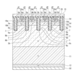
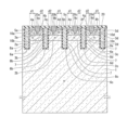
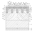
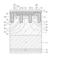
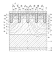
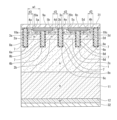
- FIG. 1 is a vertical cross-sectional view of an example of an insulated gate semiconductor device according to a first embodiment
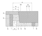
- FIG. 2 is an enlarged cross-sectional view of region A in FIG. 1
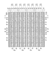
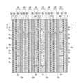
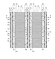
- 1 is a horizontal cross-sectional view of an example of an insulated gate semiconductor device according to a first embodiment
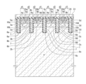
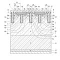
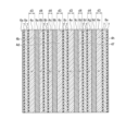
- 1 is a vertical cross-sectional view of an example of an insulated gate semiconductor device according to a first embodiment
- 5A to 5C are cross-sectional views illustrating process steps of an example of a method for manufacturing the insulated gate semiconductor device according to the first embodiment
- 6A to 6C are cross-sectional views illustrating steps in the manufacturing method of the insulated gate semiconductor device according to the first embodiment, the cross-sectional views being subsequent to FIG. 5 .
- 7A to 7C are cross-sectional views illustrating steps in the manufacturing method of the insulated gate semiconductor device according to the first embodiment, the cross-sectional views being subsequent to FIG. 6 .
- 8A to 8C are cross-sectional views illustrating steps in the manufacturing method of the insulated gate semiconductor device according to the first embodiment, the cross-sectional views being subsequent to FIG. 7.
- 9A to 9C are cross-sectional views illustrating steps in the manufacturing method of the insulated gate semiconductor device according to the first embodiment, the cross-sectional views being subsequent to FIG. 8 .
- 10A to 10C are cross-sectional views illustrating steps in the manufacturing method of the insulated gate semiconductor device according to the first embodiment, the cross-sectional views being subsequent to FIG. 9 .
- 11A to 11C are cross-sectional views illustrating the steps of the method for manufacturing the insulated gate semiconductor device according to the first embodiment, the steps being continued from FIG. 10 .
- 12A to 12C are cross-sectional views illustrating the process of the example of the method for manufacturing the insulated gate semiconductor device according to the first embodiment, which are subsequent to FIG. 11 .
- 13A to 13C are cross-sectional views illustrating the steps of the method for manufacturing the insulated gate semiconductor device according to the first embodiment, the steps being continued from FIG. 12 .
- 14A to 14C are cross-sectional views illustrating the steps of the method for manufacturing the insulated gate semiconductor device according to the first embodiment, the steps being continued from FIG. 13 .
- FIG. 11 is a vertical cross-sectional view of an example of an insulated gate semiconductor device according to a second embodiment.
- FIG. 11 is a horizontal cross-sectional view of an example of an insulated gate semiconductor device according to a second embodiment.
- FIG. 11 is a horizontal cross-sectional view of an example of an insulated gate semiconductor device according to a third embodiment.
- FIG. 13 is a vertical cross-sectional view of an example of an insulated gate semiconductor device according to a fourth embodiment.
- FIG. 13 is a vertical cross-sectional view of an example of an insulated gate semiconductor device according to a fifth embodiment.
- FIG. 23 is an enlarged cross-sectional view of region A in FIG. 22.
- FIG. 13 is a horizontal cross-sectional view of an example of an insulated gate semiconductor device according to a fifth embodiment.
- FIG. 13 is a horizontal cross-sectional view of an example of an insulated gate semiconductor device according to a sixth embodiment.
- FIG. 23 is a vertical cross-sectional view of an example of an insulated gate semiconductor device according to the seventh embodiment.
- FIG. 13 is a horizontal cross-sectional view of an example of an insulated gate semiconductor device according to an eighth embodiment.
- FIG. 13 is a vertical cross-sectional view of an example of an insulated gate semiconductor device according to a ninth embodiment.
- FIG. 23 is a vertical cross-sectional view of an example of an
- first main electrode region and the “second main electrode region” are the main electrode regions of the semiconductor element into which the main current flows.
- the “first main electrode region” means a semiconductor region that is either the emitter region or the collector region in the case of an insulated gate bipolar transistor (IGBT).
- the “first main electrode region” means a semiconductor region that is either the source region or the drain region in the case of a field effect transistor (FET) or a static induction transistor (SIT).
- FET field effect transistor
- SIT static induction transistor
- second main electrode region means a semiconductor region that is either the anode region or the cathode region in the case of a static induction thyristor (SI thyristor) or a gate turn-off thyristor (GTO).
- the "second main electrode region” means a region that is either the emitter region or the collector region, which is not the first main electrode region, in the case of an IGBT.
- the "second main electrode region” means a semiconductor region that is either the source region or the drain region, which is not the first main electrode region, in the case of a FET or a SIT. In the case of an SI thyristor or GTO, it means a region that is either an anode region or a cathode region that is not the first main electrode region. That is, if the "first main electrode region” is the source region, the “second main electrode region” means the drain region. If the "first main electrode region” is the emitter region, the “second main electrode region” means the collector region.
- the "second main electrode region” means the cathode region. Note that when the term “main electrode region” is simply used, it comprehensively means either the first main electrode region or the second main electrode region that is technically and contextually appropriate.
- the conductivity types may be selected in the opposite relationship, with the first conductivity type being p-type and the second conductivity type being n-type.
- the "+" or "-” attached to "n” or “p” means that the semiconductor region has a relatively high or low impurity concentration, respectively, compared to a semiconductor region without the "+” or "-” attached.
- the impurity concentration of each semiconductor region is strictly the same.
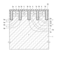
- the semiconductor device according to the first embodiment includes a drift layer 1 of a first conductivity type (n - type).
- n-type accumulation layers 2a to 2d having a higher impurity concentration than the drift layer 1 are provided.
- the lower surfaces of the accumulation layers 2a to 2d are in contact with the upper surface of the drift layer 1.
- IE effect carrier injection promotion effect
- the accumulation layers 2a to 2d are not necessarily provided.
- Base regions 3a to 3d of the second conductivity type are provided on the upper surface sides of the accumulation layers 2a to 2d.
- the lower surfaces of the base regions 3a to 3d contact the upper surfaces of the accumulation layers 2a to 2d.
- the lower surfaces of the base regions 3a to 3d contact the upper surface of the drift layer 1.
- second conductivity type (p + type) contact regions 5a to 5d having a higher impurity concentration than the base regions 3a to 3d are selectively provided.
- n + type first main electrode regions (emitter regions) 4a to 4d are provided on the upper surface side of the base regions 3a to 3d and the contact regions 5a to 5d.
- the lower surfaces of the emitter regions 4a to 4h are in contact with the upper surfaces of the base regions 3a to 3d and the contact regions 5a to 5d.
- the impurity concentration of the emitter regions 4a to 4h is higher than the impurity concentration of the drift layer 1 and the accumulation layers 2a to 2d.
- a number of trenches 6a to 6e are provided in parallel and spaced apart from each other in the depth direction, which is perpendicular to the upper surfaces of the emitter regions 4a to 4h, from the upper surfaces of the emitter regions 4a to 4h.
- the trenches 6a to 6e have the same width and depth.
- the trenches 6a to 6e reach the drift layer 1 through the emitter regions 4a to 4h, the base regions 3a to 3d, and the accumulation layers 2a to 2d.
- the side surfaces (sidewalls) of the trenches 6a to 6e are in contact with the side surfaces of the emitter regions 4a to 4h, the base regions 3a to 3d, and the accumulation layers 2a to 2d.
- the contact regions 5a to 5d are spaced apart from the trenches 6a to 6e.
- the mesa portions are provided between adjacent trenches 6a-6e.
- the mesa portions are regions sandwiched between adjacent trenches 6a-6e and above the deepest positions of the trenches 6a-6e.
- the mesa portions between the multiple trenches 6a-6e have the same width.
- the mesa portions include the upper portion of the drift layer 1, the accumulation layers 2a-2d, the base regions 3a-3d, the contact regions 5a-5d, and the emitter regions 4a-4h.
- the multiple trenches 6a to 6e include trenches 6a, 6c, and 6e that function as gates of the IGBT (hereinafter referred to as "gate trenches"), and trenches 6b and 6d that do not function as gates of the IGBT (hereinafter referred to as "dummy trenches").
- the dummy trenches 6b and 6d have the function of reducing the capacitance between the gate and the collector.
- FIG. 1 illustrates an example in which the gate trenches 6a, 6c, and 6e and the dummy trenches 6b and 6d are alternately provided, but this is not limited to this.
- two or more gate trenches may be adjacent to each other, and two or more dummy trenches may be adjacent to each other.
- a gate insulating film 7 is provided so as to cover the lower and side surfaces of the gate trenches 6a, 6c, and 6e and the dummy trenches 6b and 6d .
- the gate insulating film 7 for example, any one of a silicon dioxide film ( SiO2 film), a silicon oxynitride (SiON) film, a strontium oxide ( SrO ) film, a silicon nitride ( Si3N4 ) film, an aluminum oxide ( Al2O3 ) film, a magnesium oxide ( MgO ) film, an yttrium oxide (Y2O3 ) film, a hafnium oxide ( HfO2 ) film, a zirconium oxide ( ZrO2 ) film, a tantalum oxide ( Ta2O5 ) film, and a bismuth oxide ( Bi2O3 ) film, or a composite film in which a plurality of these films are laminated, can be used.
- SiO2 film silicon dioxide
- Gate electrodes 8a, 8c, 8e are embedded inside the gate trenches 6a, 6c, 6e via a gate insulating film 7.
- the gate insulating film 7 and the gate electrodes 8a, 8c, 8e form an insulated gate electrode structure (7, 8a), (7, 8c), (7, 8e).
- the gate electrodes 8a, 8c, 8e are electrically connected to a gate runner (not shown).
- Dummy electrodes 8b, 8d are embedded inside the dummy trenches 6b, 6d via a gate insulating film 7.
- the dummy electrodes 8b, 8d are not connected to the gate runner (not shown) but are electrically connected to an emitter electrode 31 described below.
- the material for the gate electrodes 8a, 8c, 8e and the dummy electrodes 8b, 8d for example, a polysilicon film (doped polysilicon film) to which n-type impurities such as phosphorus (P) or p-type impurities such as boron (B) are added at a high impurity concentration can be used.
- n-type impurities such as phosphorus (P) or p-type impurities such as boron (B) are added at a high impurity concentration
- the interlayer insulating film 20 is provided on the upper surfaces of the emitter regions 4a to 4h, the gate insulating film 7, the gate electrodes 8a, 8c, and 8e, and the dummy electrodes 8b and 8d.
- the interlayer insulating film 20 is composed of a single layer film such as a non-doped silicon oxide film ( SiO2 film) that does not contain phosphorus (P) or boron (B) called "NSG", a silicon oxide film (PSG film) to which phosphorus has been added, a silicon oxide film (BSG film) to which boron has been added, a silicon oxide film (BPSG film) to which boron and phosphorus have been added, a silicon nitride film ( Si3N4 film), a high-temperature oxide film (HTO film), or a laminated film of these.
- SiO2 film non-doped silicon oxide film
- P phosphorus
- B boron
- Si3N4 film silicon oxide film
- Contact holes 20a-20d are provided on the mesa portion of the interlayer insulating film 20, penetrating the interlayer insulating film 20.
- Trenches (contact trenches) 10a-10d are provided in the mesa portion so as to be continuous with the contact holes 20a-20d.
- the contact trenches 10a-10d are provided in a depth direction that is perpendicular to the upper surface of the mesa portion from the upper surface of the mesa portion.
- the upper parts of the side surfaces (sidewalls) of the contact trenches 10a-10d contact the emitter regions 4a-4h.
- the lower surfaces (bottom surfaces) and lower parts of the side surfaces (sidewalls) of the contact trenches 10a-10d contact the contact regions 5a-5d.
- Contact portions 9a-9d are embedded in the contact trenches 10a-10d and the contact holes 20a-20d. By providing contact trenches 10a-10d, contact can be made below the emitter regions 4a-4h, reducing the effect of the potential created by the hole current on the emitter regions 4a-4h and improving the latch-up resistance.
- a surface electrode (emitter electrode) 31 is provided on the interlayer insulating film 20.
- the emitter electrode 31 is electrically connected to the emitter regions 4a-4h and the contact regions 5a-5d via the contact portions 9a-9d.
- the emitter electrode 31 can be made of metals such as aluminum (Al), an Al alloy, or copper (Cu). Examples of Al alloys include Al-silicon (Si), Al-copper (Cu)-Si, and Al-Cu.
- n-type field stop (FS) layer 11 with a higher impurity concentration than the drift layer 1 is provided on the lower surface side of the drift layer 1.
- the upper surface of the FS layer 11 is in contact with the lower surface of the drift layer 1.
- the FS layer 11 prevents the depletion layer spreading from the lower surface side of the base regions 3a to 3d from reaching the second main electrode region (collector region) 12 described later.
- a p + type collector region 12 is provided on the lower surface side of the FS layer 11.
- the upper surface of the collector region 12 is in contact with the lower surface of the FS layer 11.
- the impurity concentration of the collector region 12 is higher than the impurity concentrations of the base regions 3a to 3d.
- the semiconductor region from the upper surface of the emitter regions 4a to 4h to the lower surface of the collector region 12 is composed of a semiconductor substrate.
- the semiconductor substrate is composed of, for example, a silicon (Si) substrate.
- the semiconductor substrate is not limited to a Si substrate, and may be a semiconductor substrate made of a semiconductor (wide bandgap semiconductor) having a wider band gap than Si, such as silicon carbide (SiC), gallium nitride (GaN), gallium oxide (Ga 2 O 3 ), diamond (C), or aluminum nitride (AlN).
- a back electrode (collector electrode) 32 is provided on the underside of the collector region 12.
- the collector electrode 32 can be composed of, for example, a single layer film made of gold (Au) or a metal film laminated in the order of titanium (Ti), nickel (Ni), and gold (Au).
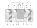
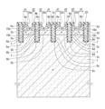
- FIG. 2 shows an enlarged view of the dashed area A surrounding the contact trench 10a in FIG. 1.
- the contact trench 10a penetrates the emitter regions 4a and 4b and reaches the contact region 5a.
- the depth of the contact trench 10a is deeper than the depth of the emitter regions 4a and 4b. Since the depth of the contact trench 10a is deeper than the depth of the emitter regions 4a and 4b, the contact region 5a can be easily expanded laterally, and the latch-up resistance can be improved.
- the depth of the contact trench 10a may be the same as the depth of the emitter regions 4a and 4b, or may be shallower than the depth of the emitter regions 4a and 4b.
- the side of the contact trench 10a has a tapered shape (forward taper shape) that narrows from the opening toward the bottom surface.
- the side of the contact trench 10a may be approximately perpendicular to the bottom surface of the contact trench 10a, or may have a tapered shape (reverse taper shape) that widens from the opening toward the bottom surface.
- the bottom surface of the contact trench 10a is flat, but is not limited to this and may be a downwardly convex curved surface, etc.
- a contact portion 9a is embedded in the contact trench 10a and the contact hole 20a.
- the upper portion of the side of the contact portion 9a is in contact with the emitter regions 4a, 4b and the interlayer insulating film 20.
- the lower portion and bottom surface of the side of the contact portion 9a are in contact with the contact region 5a. Because the lower portion and bottom surface of the side of the contact portion 9a are in contact with the contact region 5a, it is easier to ensure latch-up resistance compared to the case where only the bottom surface of the contact portion 9a is in contact with the contact region 5a.
- the contact portion 9a is in ohmic contact with the emitter regions 4a, 4b and the contact region 5a.
- the contact portion 9a is composed of, for example, a barrier metal film and a contact plug.
- a barrier metal film for example, a single layer film of titanium (Ti) or titanium nitride (TiN), or a laminate film of Ti and TiN, can be used.
- a metal such as tungsten (W) can be used.
- a metal silicide layer may be formed between the contact portion 9a and the emitter regions 4a to 4h and the contact region 5a.
- the contact portion 9a may be made of the same material as the emitter electrode 31, or may be formed integrally with the emitter electrode 31.
- the contact portion 9a may be made of a material different from the emitter material.
- the contact portion 9a includes a buried portion 91 and a plug portion 92.
- the buried portion 91 and the plug portion 92 may be formed integrally with each other or may be formed separately.
- the buried portion 91 is the lower portion of the contact portion 9a, and is the portion buried in the contact trench 10a.
- the plug portion 92 is the upper portion of the contact portion 9a, and is the portion provided in the contact hole 20a.
- the horizontal distance d1 from the end of the upper surface of the contact portion 9a on the gate electrode 8a side to the gate insulating film 7 in contact with the side of the gate electrode 8a is smaller than the horizontal distance d3 (in other words, the protruding width on the lower surface side of the interlayer insulating film 20 on the gate electrode 8a side) from the side of the contact portion 9a on the gate electrode 8a side of the contact portion 9a at a position in the horizontal direction on the lower surface of the interlayer insulating film 20 or the end of the upper surface of the emitter region 4a on the contact portion 9a side (right side) to the gate insulating film 7 in contact with the side of the gate electrode 8a.
- the end of the upper surface of the contact portion 9a on the dummy electrode 8b side is located closer to the dummy electrode 8b than the side surface of the upper surface of the contact portion 9a on the dummy electrode 8b side in the horizontal direction on the lower surface of the interlayer insulating film 20.
- the horizontal distance d2 from the end of the upper surface of the contact portion 9a on the dummy electrode 8b side to the gate insulating film 7 in contact with the side surface of the dummy electrode 8b is smaller than the horizontal distance d4 (in other words, the protruding width on the lower surface side of the interlayer insulating film 20 on the dummy electrode 8b side) from the side surface of the contact portion 9a on the dummy electrode 8b side of the contact portion 9a at a position in the horizontal direction on the lower surface of the interlayer insulating film 20, or the end of the upper surface of the emitter region 4b on the contact portion 9a side (left side) to the gate insulating film 7 in contact with the side surface of the dummy electrode 8b.
- the horizontal distance d3 from the side of the contact portion 9a on the gate electrode 8a side in the horizontal direction on the lower surface of the interlayer insulating film 20, or the end of the contact portion 9a side on the upper surface of the emitter region 4a, to the gate insulating film 7 in contact with the side of the gate electrode 8a, is greater than the horizontal distance d4 from the side of the contact portion 9a on the dummy electrode 8b side in the horizontal direction on the lower surface of the interlayer insulating film 20, or the end of the contact portion 9a side on the upper surface of the emitter region 4b, to the gate insulating film 7 in contact with the side of the dummy electrode 8b.
- the distance d3 may be about 1.5 times or more and 10 times or less than the distance d4.
- the contact trench 10b and contact portion 9b between the dummy trench 6b and gate trench 6c shown in FIG. 1 are located closer to the dummy trench 6b than a position equidistant from the dummy trench 6b and gate trench 6c.
- the contact trench 10c and contact portion 9c between the gate trench 6c and dummy trench 6d are located closer to the dummy trench 6d than a position equidistant from the gate trench 6c and dummy trench 6d.
- the contact trench 10d and contact portion 9d between the dummy trench 6d and gate trench 6e are located closer to the dummy trench 6d than a position equidistant from the dummy trench 6d and gate trench 6e.
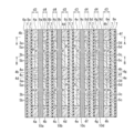
- FIG. 3 shows a horizontal cross section passing through the upper surfaces of emitter regions 4a-4h, the upper surface of gate insulating film 7, the upper surfaces of gate trenches 6a, 6c, and 6e, the upper surfaces of dummy trenches 6b and 6d, and contact trenches 10a-10d, as viewed from the B-B direction on the top side of the semiconductor device according to the first embodiment shown in FIG. 1.
- the horizontal cross section viewed from the A-A direction in FIG. 3 corresponds to FIG. 1.
- the gate trenches 6a, 6c, 6e, the dummy trenches 6b, 6d, and the contact trenches 10a to 10d have a linear (striped) planar pattern that extends parallel to one another in one direction (the vertical direction in FIG. 3).
- the emitter regions 4a to 4h have a planar pattern that is intermittently provided in one direction (the vertical direction in FIG. 3).
- the emitter region 4a and the contact region 5a are in contact with one side (left side) of the contact trench 10a.
- the emitter region 4a and the contact region 5a are in contact with each other and are arranged alternately and periodically in one direction (the vertical direction in FIG. 3).
- the emitter region 4b and the contact region 5a are in contact with each other and are arranged alternately and periodically in one direction (the vertical direction in FIG. 3).
- the one direction (the vertical direction in FIG. 3) indicates the direction in which the gate trenches 6a, 6c, 6e, the dummy trenches 6b, 6d, and the contact trenches 10a to 10d extend parallel to each other. Note that the one side (left side) and the other side (right side) are perpendicular to the one direction (the vertical direction in FIG. 3).
- the emitter region 4c and the contact region 5b are in contact with one side surface (left side) of the contact trench 10b.
- the emitter region 4c and the contact region 5b are in contact with each other and are arranged alternately and periodically in one direction (the vertical direction in FIG. 3).
- the emitter region 4d and the contact region 5b are in contact with the other side surface (right side) of the contact trench 10b.
- the emitter region 4d and the contact region 5b are in contact with each other and are arranged alternately and periodically in one direction (the vertical direction in FIG. 3).
- the emitter region 4e and the contact region 5c are in contact with one side (left side) of the contact trench 10c.
- the emitter region 4e and the contact region 5c are in contact with each other and are arranged alternately and periodically in one direction (the vertical direction in FIG. 3).
- the emitter region 4f and the contact region 5c are in contact with the other side (right side) of the contact trench 10c.
- the emitter region 4f and the contact region 5c are in contact with each other and are arranged alternately and periodically in one direction (the vertical direction in FIG. 3).
- the emitter region 4g and the contact region 5d are in contact with one side (left side) of the contact trench 10d.
- the emitter region 4g and the contact region 5d are in contact with each other and are arranged alternately and periodically in one direction (the up-down direction in FIG. 3).
- the emitter region 4h and the contact region 5d are in contact with the other side (right side) of the contact trench 10d.
- the emitter region 4h and the contact region 5d are in contact with each other and are arranged alternately and periodically in one direction (the up-down direction in FIG. 3).
- FIG. 4 is a vertical cross-sectional view taken from the B-B direction in FIG. 3, at a position where the emitter regions 4a-4h do not pass.
- the upper surfaces of the contact regions 5a-5d are in contact with the interlayer insulating film 20. Because the entire side surfaces and lower surfaces of the contact portions 9a-9d are in contact with the contact regions 5a-5d, it is easier to ensure latch-up resistance compared to when only the lower surfaces of the contact portions 9a-9d, or only the lower surfaces and lower parts of the side surfaces of the contact portions 9a-9d, are in contact with the contact regions 5a-5d.
- the emitter electrode 31 when the emitter electrode 31 is at ground potential, a positive voltage is applied to the collector electrode 32, and a positive voltage equal to or greater than the threshold is applied to the gate electrodes 8a, 8c, and 8e, an inversion layer (channel) is formed on the side of the gate trenches 6a, 6c, and 6e in the base regions 3a to 3d, resulting in an ON state.
- a current flows from the collector electrode 32 to the emitter electrode 31 via the collector region 12, the FS layer 11, the drift layer 1, the accumulation layers 2a to 2d, the inversion layers in the base regions 3a to 3d, and the emitter regions 4a, 4d, 4e, and 4h.
- the dummy trenches 6b and 6d are provided adjacent to the gate trenches 6a, 6c, and 6e, a part of the gate-collector capacitance (feedback capacitance) is replaced by the collector-emitter capacitance, thereby reducing the feedback capacitance and improving the switching speed.
- the voltage applied to the gate electrodes 8a, 8c, and 8e is less than the threshold value, no inversion layer is formed in the base regions 3a to 3d, so the device is in the off state and no current flows from the collector electrode 32 to the emitter electrode 31.
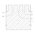
- a semiconductor substrate made of a first conductivity type (n - type) silicon (Si) wafer or the like is prepared.
- This semiconductor substrate functions as the drift layer 1.
- a part of the upper part of the drift layer 1 is selectively removed by photolithography technology and dry etching.
- a plurality of trenches 6a to 6e are formed in the upper part of the drift layer 1, as shown in FIG. 5.
- the plurality of trenches 6a to 6e include gate trenches 6a, 6c, and 6e and dummy trenches 6b and 6d.
- a gate insulating film 7 is formed on the bottom and side surfaces of the gate trenches 6a, 6c, 6e and the dummy trenches 6b, 6d by thermal oxidation or chemical vapor deposition (CVD).
- a polysilicon film doped polysilicon film to which impurities such as phosphorus (P) and boron (B) are added at a high concentration is deposited by CVD or the like so as to fill the inside of the gate trenches 6a, 6c, 6e and the dummy trenches 6b, 6d through the gate insulating film 7.
- the polysilicon film and the gate insulating film 7 on the drift layer 1 are selectively removed by photolithography and dry etching.
- an insulated gate electrode structure (7, 8a), (7, 8c), (7, 8e) consisting of the gate insulating film 7 and the gate electrodes 8a, 8c, 8e of the polysilicon film is formed inside the gate trenches 6a, 6c, 6e. Additionally, a gate insulating film 7 and dummy electrodes 8b and 8d are formed inside the dummy trenches 6b and 6d.
- p - type impurities such as boron (B) are ion-implanted on the entire upper surface of the drift layer 1 to form p-type base regions 3a to 3d.
- n-type impurities such as phosphorus (P) or arsenic (As) are ion-implanted on the entire upper surface of the drift layer 1 to form n-type accumulation layers 2a to 2d.
- a photoresist film is applied to the upper surface of the drift layer 1, and the photoresist film is patterned by photolithography.
- n-type impurities such as phosphorus (P) or arsenic (As) are ion-implanted to form n + type emitter regions 4a to 4h. Then, the photoresist film is removed.
- the order of ion implantation for forming the accumulation layers 2a to 2d, ion implantation for forming the base regions 3a to 3d, and ion implantation for forming the emitter regions 4a to 4h is not particularly limited, and the order may be changed.
- n-type accumulation layers 2a-2d, p - type base regions 3a-3d, and n + type emitter regions 4 are formed on the drift layer 1.
- the emitter regions 4 are formed intermittently in the depth direction of Fig. 7.
- an interlayer insulating film 20 is formed on the upper surfaces of the gate insulating film 7, the gate electrodes 8a, 8c, and 8e, the dummy electrodes 8b and 8d, and the emitter region 4 by CVD or the like.
- a photoresist film is applied to the upper surface of the interlayer insulating film 20, and the photoresist film is patterned using photolithography technology. Using the patterned photoresist film as an etching mask, a portion of the interlayer insulating film 20 is selectively removed by dry etching. The photoresist film is then removed. As a result, as shown in FIG. 9, contact holes 20a to 20d are opened in the interlayer insulating film 20, exposing a portion of the upper surface of the emitter region 4.
- the contact holes 20a to 20d are opened so that the horizontal distance d1 from the end of the opening of the contact holes 20a to 20d on the gate electrode 8a, 8c, 8e side to the gate insulating film 7 on the gate electrode 8a, 8c, 8e side (the overhang width on the upper surface side of the interlayer insulating film 20 on the gate electrode 8a, 8c, 8e side) is greater than the horizontal distance d2 from the end of the opening of the contact holes 20a to 20d on the dummy electrode 8b, 8d side to the gate insulating film 7 on the dummy electrode 8b, 8d side (in other words, the overhang width on the upper surface side of the interlayer insulating film 20 on the dummy electrode 8b, 8d side).
- the emitter region 4 of the mesa portion and a portion of the base regions 3a to 3d are selectively removed by dry etching such as reactive ion etching (RIE).
- dry etching such as reactive ion etching (RIE).
- RIE reactive ion etching
- p-type impurities such as boron (B) are ion-implanted using the interlayer insulating film 20 as an ion-implantation mask.
- the implanted p-type impurities are then activated by heat treatment.
- p + type contact regions 5a to 5d are formed in the upper portions of the base regions 3a to 3d, in contact with the lower surfaces and lower portions of the side surfaces of the contact trenches 10a to 10d.
- a barrier metal film such as titanium (Ti) and titanium nitride (TiN) is formed in the contact trenches 10a-10d and the contact holes 20a-20d by sputtering or vapor deposition, dry etching, etc.
- contact plugs such as tungsten (W) are embedded in the contact trenches 10a-10d and the contact holes 20a-20d via the barrier metal film by CVD, etch-back, etc.
- contact sections 9a-9d consisting of the barrier metal film and contact plugs are embedded in the contact trenches 10a-10d and the contact holes 20a-20d.
- the emitter electrode 31 is deposited on the upper surfaces of the contact portions 9a to 9d and the interlayer insulating film 20 by sputtering or vapor deposition, as shown in FIG. 13.
- the drift layer 1 is ground from the lower surface side by grinding or chemical mechanical polishing (CMP), etc., and the thickness of the drift layer 1 is adjusted to the product thickness.
- n-type impurities such as phosphorus (P) or selenium (Se) are ion-implanted over the entire lower surface of the drift layer 1 to form an n-type FS layer 11.
- p - type impurities such as boron (B) are ion-implanted over the entire lower surface of the drift layer 1 at an acceleration voltage lower than the acceleration voltage of the ion implantation to form the n-type FS layer 11.
- the implanted impurity ions are activated by heat treatment. As a result, as shown in FIG. 14, an n-type FS layer 11 and a p + type collector region 12 are formed in the lower part of the drift layer 1.
- a collector electrode 32 made of gold (Au) or the like is formed on the entire lower surface of the collector region 12 by sputtering, vapor deposition, or the like.
- the semiconductor substrate is then cut (diced) into individual pieces to complete the semiconductor device according to the first embodiment shown in Figures 1 to 4.
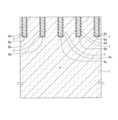
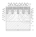
- Fig. 15 is a vertical cross-sectional view of the semiconductor device according to the comparative example, which corresponds to the vertical cross-sectional view of the semiconductor device according to the first embodiment shown in Fig. 1.
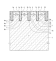
- Fig. 16 is a horizontal cross-sectional view of the semiconductor device according to the comparative example, which corresponds to the horizontal cross-sectional view of the semiconductor device according to the first embodiment shown in Fig. 2.
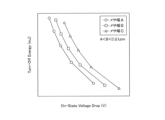
- the semiconductor device according to the comparative example differs from the semiconductor device according to the first embodiment shown in Figures 1 and 2 in that contact trenches 10a to 10d and contact portions 9a to 9d are provided in the center of the mesa portion, which is equidistant from gate trenches 6a, 6c, and 6e and dummy trenches 6b and 6d.
- the horizontal distance d11 from the end of the upper surface of the contact portions 9a to 9d on the gate electrode 8a, 8c, 8e side to the gate insulating film 7 on the gate electrode 8a, 8c, 8e side is equal to the horizontal distance d11 from the end of the upper surface of the contact portions 9a to 9d on the dummy electrode 8b, 8d side to the gate insulating film 7 on the dummy electrode 8b, 8d side.
- the contact trenches 10a-10d and the contact portions 9a-9d sandwiched between the gate trenches 6a, 6c, 6e and the dummy trenches 6b, 6d are positioned closer to the dummy trenches 6b, 6d than to the center of the mesa portion.
- Fig. 18 is a vertical cross-sectional view of an insulated gate semiconductor device according to a second embodiment, which corresponds to the vertical cross-sectional view of the semiconductor device according to the first embodiment shown in Fig. 1.
- Fig. 19 is a horizontal cross-sectional view of an insulated gate semiconductor device according to a second embodiment, which corresponds to the horizontal cross-sectional view of the semiconductor device according to the first embodiment shown in Fig. 2.
- the insulated gate semiconductor device according to the second embodiment differs from the insulated gate semiconductor device according to the first embodiment shown in Figures 1 and 2 in that only emitter regions 4a, 4d, 4e, and 4h are provided on the gate trenches 6a, 6c, and 6e sides, and no emitter regions are provided on the dummy trenches 6b and 6d sides.
- the contact trenches 10a-10d and contact portions 9a-9d sandwiched between the gate trenches 6a, 6c, 6e and the dummy trenches 6b, 6d are positioned closer to the dummy trenches 6b, 6d than to the center of the mesa portion. This allows the mesa width w1 to be narrowed, enhancing the IE effect and improving the trade-off characteristics between the on-voltage Von and the turn-off loss Eoff.
- a vertical cross-sectional view of the insulated gate semiconductor device according to the third embodiment is similar to the vertical cross-sectional view of the semiconductor device according to the second embodiment shown in Fig. 18.
- the insulated gate semiconductor device according to the third embodiment is similar to the insulated gate semiconductor device according to the second embodiment shown in Fig. 19 in that only emitter regions 4a, 4d, 4e, and 4h are provided on the gate trenches 6a, 6c, and 6e sides, and no emitter regions are provided on the dummy trenches 6b and 6d sides.
- FIG. 20 is a horizontal cross-sectional view of an insulated gate semiconductor device according to a third embodiment, which corresponds to the horizontal cross-sectional view of the semiconductor device according to the second embodiment shown in FIG. 19.
- the insulated gate semiconductor device according to the third embodiment differs from the insulated gate semiconductor device according to the second embodiment shown in FIG. 19 in that the emitter regions 4a, 4d, 4e, and 4h have a planar pattern extending in stripes in one direction (the vertical direction in FIG. 20).
- Other configurations of the insulated gate semiconductor device according to the third embodiment are substantially similar to those of the insulated gate semiconductor device according to the second embodiment, and therefore repeated explanations will be omitted.
- the contact trenches 10a-10d and contact portions 9a-9d sandwiched between the gate trenches 6a, 6c, 6e and the dummy trenches 6b, 6d are positioned closer to the dummy trenches 6b, 6d than to the center of the mesa portion. This allows the mesa width w1 to be narrowed, enhancing the IE effect and improving the trade-off characteristics between the on-voltage Von and the turn-off loss Eoff.
- FIG. 21 is a vertical cross-sectional view of an insulated gate semiconductor device according to the fourth embodiment, and corresponds to the vertical cross-sectional view of the semiconductor device according to the second embodiment shown in FIG.
- the insulated gate type semiconductor device according to the fourth embodiment is similar to the insulated gate type semiconductor device according to the second embodiment shown in FIG. 18 in that only emitter regions 4a, 4d, 4e, and 4h are provided on the gate trenches 6a, 6c, and 6e sides, and no emitter regions are provided on the dummy trenches 6b and 6d sides.
- the insulated gate type semiconductor device according to the fourth embodiment differs from the insulated gate type semiconductor device according to the second embodiment in that the contact regions 5a to 5d are in contact with the dummy trenches 6b and 6d.
- Other configurations of the insulated gate type semiconductor device according to the fourth embodiment are substantially similar to those of the insulated gate type semiconductor device according to the second embodiment, so duplicated explanations will be omitted.
- the contact trenches 10a-10d and contact portions 9a-9d sandwiched between the gate trenches 6a, 6c, 6e and the dummy trenches 6b, 6d are positioned closer to the dummy trenches 6b, 6d than to the center of the mesa portion. This allows the mesa width w1 to be narrowed, enhancing the IE effect and improving the trade-off characteristics between the on-voltage Von and the turn-off loss Eoff.
- FIG. 22 is a vertical cross-sectional view of an insulated gate semiconductor device according to the third embodiment, and corresponds to the vertical cross-sectional view of the semiconductor device according to the first embodiment shown in FIG.
- the insulated gate semiconductor device according to the fifth embodiment differs from the insulated gate semiconductor device according to the first embodiment shown in FIG. 1 in that contact holes 20a, 20c and contact trenches 10a, 10c are provided above dummy trenches 6b, 6d, as shown in FIG. 22.
- the upper part of the side of contact trench 10a is in contact with the interlayer insulating film 20 and emitter regions 4a, 4d.
- the lower part and bottom surface of the side of contact trench 10a are in contact with contact regions 5a, 5b.
- the upper part of the side of contact trench 10c is in contact with the interlayer insulating film 20 and emitter regions 4e, 4h.
- the lower part and bottom surface of the side of contact trench 10c are in contact with contact regions 5c, 5d.
- the contact portions 9a, 9c embedded in the contact holes 20a, 20c and the contact trenches 10a, 10c contact the dummy electrodes 8b, 8d embedded in the dummy trenches 6b, 6d.
- a p-layer may be formed on the surface of the dummy electrodes 8b, 8d during ion implantation to form the contact regions 5a to 5d after the contact trenches 10a, 10c are formed, and a pn junction may be formed in the dummy electrodes 8b, 8d.
- the lower surface side of the dummy trenches 6b, 6d becomes a high voltage
- the potential of the dummy electrodes 8b, 8d becomes a floating potential, and the breakdown voltage decreases.
- the dummy electrodes 8b, 8d are made of polysilicon doped with p-type impurities, a pn junction is not formed in the dummy electrodes 8b, 8d during ion implantation to form the contact regions 5a to 5d, but the gate electrodes 8a, 8c, 8e formed at the same time as the dummy electrodes 8b, 8d are also made of polysilicon doped with p-type impurities, so the conductivity decreases.
- the dummy electrodes 8b, 8d are made of doped polysilicon with a high impurity concentration, in which n-type impurities such as phosphorus (P) are contained up to the solid solubility limit. This makes it possible to prevent a p-layer from being formed on the surface layers of the dummy electrodes 8b, 8d during ion implantation to form the contact regions 5a-5d, and also to prevent a decrease in conductivity.
- the impurity concentration of the contact regions 5a-5d may be adjusted to such an extent that a p-layer is not formed on the surface layers of the dummy electrodes 8b, 8d during ion implantation to form the contact regions 5a-5d.
- FIG. 23 shows an enlarged view of the dashed area A surrounding the contact trench 10a in FIG. 22.
- the depth of the contact trench 10a is deeper than the depth of the emitter region 4a. By making the contact trench 10a deeper than the depth of the emitter region 4a, it becomes easier to expand the contact region 5a laterally, and the latch-up resistance can be improved.
- the depth of the contact trench 10a may be the same as the depth of the emitter region 4a, or may be shallower than the depth of the emitter region 4a.
- the side of the contact trench 10a has a tapered shape (forward taper shape) that narrows from the opening toward the bottom surface.
- the side of the contact trench 10a may be approximately perpendicular to the bottom surface of the contact trench 10a, or may have a tapered shape (reverse taper shape) that widens from the opening toward the bottom surface.
- the bottom surface of the contact trench 10a is flat, but is not limited to this and may be a downwardly convex curved surface, etc.
- a contact portion 9a is embedded in the contact trench 10a and the contact hole 20a.
- the upper portion of the side of the contact portion 9a contacts the emitter region 4a and the interlayer insulating film 20.
- the lower portion of the side and the underside of the contact portion 9a contact the contact region 5a.
- the contact portion 9a includes a buried portion 91, which is the portion embedded in the contact trench 10a, and a plug portion 92, which is the portion provided in the contact hole 20a.
- the contact trench 10a and the contact portion 9a are provided closer to the dummy trench 6b than a position equidistant from the gate trench 6a and the dummy trench 6b, and at a position including the upper side of the dummy trench 6b.
- FIG. 24 shows a horizontal cross section passing through emitter regions 4a, 4d, 4e, 4h, the upper surface of gate insulating film 7, the upper surfaces of gate trenches 6a, 6c, 6e, and contact trenches 10a, 10c, as viewed from the B-B direction on the top side of the semiconductor device according to the fifth embodiment shown in FIG. 22.
- the horizontal cross section viewed from the A-A direction in FIG. 24 corresponds to FIG. 22.
- dummy trenches 6b, 6d, gate insulating film 7, and dummy electrodes 8b, 8d hidden under contact trenches 10a, 10c are shown typically by dashed lines.
- the gate trenches 6a, 6c, 6e, dummy trenches 6b, 6d, and contact trenches 10a to 10d have linear (striped) planar patterns extending parallel to one another in one direction (the vertical direction in FIG. 24).
- the emitter regions 4a to 4h have planar patterns that are intermittently provided in one direction (the vertical direction in FIG. 24).
- the other configurations of the insulated gate semiconductor device according to the fifth embodiment are substantially similar to those of the insulated gate semiconductor device according to the first embodiment, and therefore will not be described again.
- the contact trenches 10a, 10c and the contact portions 9a, 9c are positioned closer to the dummy trenches 6b, 6d than to the center of the mesa portion. This allows the mesa width w1 to be narrowed, enhancing the IE effect and improving the trade-off characteristics between the on-voltage Von and the turn-off loss Eoff.
- the mesa width w1 can be made narrower than that of the insulated gate semiconductor device according to the first embodiment by providing contact holes 20a, 20c and contact trenches 10a, 10c above the dummy trenches 6b, 6d.
- a vertical cross-sectional view of the insulated gate semiconductor device according to the sixth embodiment is similar to the vertical cross-sectional view of the semiconductor device according to the fifth embodiment shown in Fig. 22.
- the insulated gate semiconductor device according to the sixth embodiment is similar to the insulated gate semiconductor device according to the fifth embodiment shown in Fig. 22 in that contact holes 20a, 20c and contact trenches 10a, 10c are provided above dummy trenches 6b, 6d.
- FIG. 25 is a horizontal cross-sectional view of an insulated gate semiconductor device according to a sixth embodiment, which corresponds to the horizontal cross-sectional view of the semiconductor device according to the fifth embodiment shown in FIG. 24.
- the insulated gate semiconductor device according to the sixth embodiment differs from the insulated gate semiconductor device according to the fifth embodiment shown in FIG. 24 in that the emitter regions 4a, 4d, 4e, and 4h have a planar pattern extending in stripes in one direction (the vertical direction in FIG. 25).
- Other configurations of the insulated gate semiconductor device according to the sixth embodiment are substantially similar to those of the insulated gate semiconductor device according to the fifth embodiment, and therefore repeated explanations will be omitted.
- the contact trenches 10a, 10c and the contact portions 9a, 9c are moved closer to the dummy trenches 6b, 6d than to the center of the mesa portion. This allows the mesa width w1 to be narrowed, enhancing the IE effect and improving the trade-off characteristics between the on-voltage Von and the turn-off loss Eoff.
- the mesa width w1 can be made narrower than that of the insulated gate semiconductor device according to the first embodiment by providing contact holes 20a, 20c and contact trenches 10a, 10c above the dummy trenches 6b, 6d.
- FIG. 26 is a vertical cross-sectional view of an insulated gate semiconductor device according to the seventh embodiment, and corresponds to the vertical cross-sectional view of the semiconductor device according to the first embodiment shown in FIG.
- the insulated gate type semiconductor device according to the seventh embodiment differs from the insulated gate type semiconductor device according to the first embodiment in that, as shown in FIG. 26, dummy trenches 6b, 6d are provided adjacent to each other, and contact holes 20a and contact trenches 10a are provided above the dummy trenches 6b, 6d.
- the contact portions 9a embedded in the contact holes 20a and contact trenches 10a are in contact with dummy electrodes 8b, 8d embedded in the dummy trenches 6b, 6d.
- the other configurations of the insulated gate type semiconductor device according to the seventh embodiment are substantially similar to those of the insulated gate type semiconductor device according to the first embodiment, and therefore will not be described again.
- the contact trench 10a and the contact portion 9a are closer to the dummy trenches 6b and 6d than to the center of the mesa portion. This allows the mesa width to be narrowed, enhancing the IE effect and improving the trade-off characteristics between the on-voltage Von and the turn-off loss Eoff.
- the mesa width can be made narrower than that of the insulated gate semiconductor device according to the first embodiment by providing contact hole 20a and contact trench 10a above dummy trenches 6b and 6d.
- a vertical cross-sectional view of the insulated gate semiconductor device according to the eighth embodiment is similar to the vertical cross-sectional view of the semiconductor device according to the first embodiment shown in FIG.
- FIG. 27 is a horizontal cross-sectional view of an insulated gate semiconductor device according to the eighth embodiment, which corresponds to the horizontal cross-sectional view of the semiconductor device according to the first embodiment shown in FIG. 3.
- the insulated gate semiconductor device according to the eighth embodiment differs from the insulated gate semiconductor device according to the first embodiment shown in FIG. 3 in that the emitter regions 4a to 4h have a planar pattern extending in stripes in one direction (the vertical direction in FIG. 27).
- Other configurations of the insulated gate semiconductor device according to the eighth embodiment are substantially similar to those of the insulated gate semiconductor device according to the first embodiment, so redundant explanations will be omitted.
- the contact trenches 10a-10d and the contact portions 9a-9d are positioned closer to the dummy trenches 6b, 6d than to the center of the mesa portion. This allows the mesa width w1 to be narrowed, enhancing the IE effect and improving the trade-off characteristics between the on-voltage Von and the turn-off loss Eoff.
- FIG. 28 is a vertical cross-sectional view of an insulated gate semiconductor device according to the ninth embodiment, and corresponds to the vertical cross-sectional view of the semiconductor device according to the first embodiment shown in FIG.
- the insulated gate semiconductor device according to the ninth embodiment differs from the insulated gate semiconductor device according to the first embodiment shown in FIG. 1 in that there is no interlayer insulating film 20 between the emitter regions 4a to 4h and the emitter electrode 31, and the upper surfaces of the gate electrodes 8a, 8c, and 8e and the dummy electrodes 8b and 8d are covered with a gate insulating film 7.
- the other configurations of the insulated gate semiconductor device according to the ninth embodiment are substantially similar to those of the insulated gate semiconductor device according to the first embodiment, so duplicated explanations will be omitted.
- the contact trenches 10a-10d and contact portions 9a-9d sandwiched between the gate trenches 6a, 6c, 6e and the dummy trenches 6b, 6d are positioned closer to the dummy trenches 6b, 6d than to the center of the mesa portion. This allows the mesa width w1 to be narrowed, enhancing the IE effect and improving the trade-off characteristics between the on-voltage Von and the turn-off loss Eoff.
- FIG. 29 is a vertical cross-sectional view of the insulated gate semiconductor device according to the tenth embodiment, and corresponds to the vertical cross-sectional view of the semiconductor device according to the fifth embodiment shown in FIG.
- the insulated gate semiconductor device according to the tenth embodiment differs from the insulated gate semiconductor device according to the fifth embodiment shown in FIG. 22 in that there is no interlayer insulating film 20 between the emitter regions 4a, 4d, 4e, 4h and the emitter electrode 31, and the upper surfaces of the gate electrodes 8a, 8c, 8e are covered with a gate insulating film 7.
- the other configurations of the insulated gate semiconductor device according to the tenth embodiment are substantially similar to those of the insulated gate semiconductor device according to the fifth embodiment, so duplicated explanations will be omitted.
- the contact trenches 10a, 10b and the contact portions 9a, 9b are moved closer to the dummy trenches 6b, 6d than to the center of the mesa portion. This makes it possible to narrow the mesa width w1, thereby enhancing the IE effect and improving the trade-off characteristics between the on-voltage Von and the turn-off loss Eoff.
- the present invention can also be applied to a reverse conducting IGBT (RC-IGBT) or a reverse blocking insulated gate bipolar transistor (RB-IGBT).
- RC-IGBT reverse conducting IGBT
- RB-IGBT reverse blocking insulated gate bipolar transistor
- the present invention can also be applied to a MOSFET having a configuration in which the p + type collector region 12 of the IGBT shown in FIG. 1 is replaced with an n + type drain region.
Landscapes
- Electrodes Of Semiconductors (AREA)
Priority Applications (4)
| Application Number | Priority Date | Filing Date | Title |
|---|---|---|---|
| JP2025545509A JPWO2025057569A1 (cg-RX-API-DMAC7.html) | 2023-09-14 | 2024-07-23 | |
| DE112024000480.6T DE112024000480T5 (de) | 2023-09-14 | 2024-07-23 | Halbleitervorrichtung mit isoliertem gate |
| CN202480015523.5A CN120731672A (zh) | 2023-09-14 | 2024-07-23 | 绝缘栅型半导体装置 |
| US19/312,516 US20250380440A1 (en) | 2023-09-14 | 2025-08-28 | Insulated gate semiconductor device |
Applications Claiming Priority (2)
| Application Number | Priority Date | Filing Date | Title |
|---|---|---|---|
| JP2023149076 | 2023-09-14 | ||
| JP2023-149076 | 2023-09-14 |
Related Child Applications (1)
| Application Number | Title | Priority Date | Filing Date |
|---|---|---|---|
| US19/312,516 Continuation US20250380440A1 (en) | 2023-09-14 | 2025-08-28 | Insulated gate semiconductor device |
Publications (1)
| Publication Number | Publication Date |
|---|---|
| WO2025057569A1 true WO2025057569A1 (ja) | 2025-03-20 |
Family
ID=95022011
Family Applications (1)
| Application Number | Title | Priority Date | Filing Date |
|---|---|---|---|
| PCT/JP2024/026284 Ceased WO2025057569A1 (ja) | 2023-09-14 | 2024-07-23 | 絶縁ゲート型半導体装置 |
Country Status (5)
| Country | Link |
|---|---|
| US (1) | US20250380440A1 (cg-RX-API-DMAC7.html) |
| JP (1) | JPWO2025057569A1 (cg-RX-API-DMAC7.html) |
| CN (1) | CN120731672A (cg-RX-API-DMAC7.html) |
| DE (1) | DE112024000480T5 (cg-RX-API-DMAC7.html) |
| WO (1) | WO2025057569A1 (cg-RX-API-DMAC7.html) |
Families Citing this family (1)
| Publication number | Priority date | Publication date | Assignee | Title |
|---|---|---|---|---|
| JP2024098458A (ja) * | 2023-01-10 | 2024-07-23 | 富士電機株式会社 | 半導体装置 |
Citations (4)
| Publication number | Priority date | Publication date | Assignee | Title |
|---|---|---|---|---|
| JP2014060386A (ja) * | 2012-08-21 | 2014-04-03 | Rohm Co Ltd | 半導体装置 |
| JP2019186261A (ja) * | 2018-04-02 | 2019-10-24 | 富士電機株式会社 | 絶縁ゲート型半導体装置 |
| US20200066870A1 (en) * | 2018-08-22 | 2020-02-27 | Infineon Technologies Ag | Power Semiconductor Device with Self-Aligned Source Region |
| JP2023096841A (ja) * | 2021-12-27 | 2023-07-07 | 富士電機株式会社 | 半導体装置およびその製造方法 |
-
2024
- 2024-07-23 WO PCT/JP2024/026284 patent/WO2025057569A1/ja not_active Ceased
- 2024-07-23 JP JP2025545509A patent/JPWO2025057569A1/ja active Pending
- 2024-07-23 CN CN202480015523.5A patent/CN120731672A/zh active Pending
- 2024-07-23 DE DE112024000480.6T patent/DE112024000480T5/de active Pending
-
2025
- 2025-08-28 US US19/312,516 patent/US20250380440A1/en active Pending
Patent Citations (4)
| Publication number | Priority date | Publication date | Assignee | Title |
|---|---|---|---|---|
| JP2014060386A (ja) * | 2012-08-21 | 2014-04-03 | Rohm Co Ltd | 半導体装置 |
| JP2019186261A (ja) * | 2018-04-02 | 2019-10-24 | 富士電機株式会社 | 絶縁ゲート型半導体装置 |
| US20200066870A1 (en) * | 2018-08-22 | 2020-02-27 | Infineon Technologies Ag | Power Semiconductor Device with Self-Aligned Source Region |
| JP2023096841A (ja) * | 2021-12-27 | 2023-07-07 | 富士電機株式会社 | 半導体装置およびその製造方法 |
Also Published As
| Publication number | Publication date |
|---|---|
| DE112024000480T5 (de) | 2025-11-27 |
| CN120731672A (zh) | 2025-09-30 |
| US20250380440A1 (en) | 2025-12-11 |
| JPWO2025057569A1 (cg-RX-API-DMAC7.html) | 2025-03-20 |
Similar Documents
| Publication | Publication Date | Title |
|---|---|---|
| JP7563526B2 (ja) | 絶縁ゲート型半導体装置の製造方法 | |
| US10199455B2 (en) | Dual-gate trench IGBT with buried floating P-type shield | |
| CN103794653B (zh) | 带有很高的衬底-栅极击穿和嵌入式雪崩箝位二极管的横向超级结器件 | |
| CN114497200B (zh) | 半导体元件、半导体装置 | |
| JP7625903B2 (ja) | 絶縁ゲート型半導体装置 | |
| JP7647239B2 (ja) | 半導体装置 | |
| JP7643621B2 (ja) | 半導体装置 | |
| JP2024053119A (ja) | 半導体装置及びその製造方法 | |
| US10998264B2 (en) | Dual-gate trench IGBT with buried floating P-type shield | |
| JP2019106483A (ja) | 絶縁ゲート型半導体装置及びその製造方法 | |
| JP4456013B2 (ja) | 半導体装置 | |
| US12635214B2 (en) | Semiconductor device and method of manufacturing the same | |
| JP2006278826A (ja) | 半導体素子及びその製造方法 | |
| JP5878331B2 (ja) | 半導体装置及びその製造方法 | |
| JP2020136472A (ja) | 半導体装置 | |
| JP2019087646A (ja) | 半導体装置 | |
| CN103035692A (zh) | 半导体装置 | |
| JP7068994B2 (ja) | 半導体装置 | |
| US20240170569A1 (en) | Semiconductor device and method of manufacturing the same | |
| JP2025078881A (ja) | 半導体装置 | |
| CN117637473A (zh) | 半导体装置的制造方法 | |
| WO2022137789A1 (ja) | 絶縁ゲート型半導体装置 | |
| US20250380440A1 (en) | Insulated gate semiconductor device | |
| JP7099013B2 (ja) | 絶縁ゲート型半導体装置 | |
| CN114628502A (zh) | 半导体装置及半导体装置的制造方法 |
Legal Events
| Date | Code | Title | Description |
|---|---|---|---|
| WWE | Wipo information: entry into national phase |
Ref document number: 202480015523.5 Country of ref document: CN |
|
| WWE | Wipo information: entry into national phase |
Ref document number: 112024000480 Country of ref document: DE |
|
| ENP | Entry into the national phase |
Ref document number: 2025545509 Country of ref document: JP Kind code of ref document: A |
|
| WWE | Wipo information: entry into national phase |
Ref document number: 2025545509 Country of ref document: JP |
|
| WWP | Wipo information: published in national office |
Ref document number: 202480015523.5 Country of ref document: CN |
|
| WWP | Wipo information: published in national office |
Ref document number: 112024000480 Country of ref document: DE |