WO2025047331A1 - 半導体装置の製造方法、および半導体装置 - Google Patents
半導体装置の製造方法、および半導体装置 Download PDFInfo
- Publication number
- WO2025047331A1 WO2025047331A1 PCT/JP2024/028036 JP2024028036W WO2025047331A1 WO 2025047331 A1 WO2025047331 A1 WO 2025047331A1 JP 2024028036 W JP2024028036 W JP 2024028036W WO 2025047331 A1 WO2025047331 A1 WO 2025047331A1
- Authority
- WO
- WIPO (PCT)
- Prior art keywords
- sealing resin
- support portion
- semiconductor device
- region
- dimension
- Prior art date
- Legal status (The legal status is an assumption and is not a legal conclusion. Google has not performed a legal analysis and makes no representation as to the accuracy of the status listed.)
- Pending
Links
Images










Classifications
-
- H—ELECTRICITY
- H10—SEMICONDUCTOR DEVICES; ELECTRIC SOLID-STATE DEVICES NOT OTHERWISE PROVIDED FOR
- H10W—GENERIC PACKAGES, INTERCONNECTIONS, CONNECTORS OR OTHER CONSTRUCTIONAL DETAILS OF DEVICES COVERED BY CLASS H10
- H10W70/00—Package substrates; Interposers; Redistribution layers [RDL]
- H10W70/40—Leadframes
-
- H—ELECTRICITY
- H10—SEMICONDUCTOR DEVICES; ELECTRIC SOLID-STATE DEVICES NOT OTHERWISE PROVIDED FOR
- H10W—GENERIC PACKAGES, INTERCONNECTIONS, CONNECTORS OR OTHER CONSTRUCTIONAL DETAILS OF DEVICES COVERED BY CLASS H10
- H10W74/00—Encapsulations, e.g. protective coatings
-
- H—ELECTRICITY
- H10—SEMICONDUCTOR DEVICES; ELECTRIC SOLID-STATE DEVICES NOT OTHERWISE PROVIDED FOR
- H10W—GENERIC PACKAGES, INTERCONNECTIONS, CONNECTORS OR OTHER CONSTRUCTIONAL DETAILS OF DEVICES COVERED BY CLASS H10
- H10W74/00—Encapsulations, e.g. protective coatings
- H10W74/01—Manufacture or treatment
Definitions
- This disclosure relates to a method for manufacturing a semiconductor device and a semiconductor device obtained by the manufacturing method.
- the semiconductor device disclosed in Patent Document 1 comprises a semiconductor element, a first lead that is electrically connected to the semiconductor element, a second lead on which the semiconductor element is mounted, and a sealing resin that covers the semiconductor element. Each of the first lead and the second lead protrudes from the sealing resin.
- the second lead of the semiconductor device disclosed in Patent Document 1 has a second pad on which a semiconductor element is mounted.
- a protrusion is provided on the second pad.
- the protrusion protrudes in a direction perpendicular to the normal direction of the second pad surface facing the semiconductor element.
- the protrusion provided on the second pad may be used as a support member connecting the lead frame and the second lead.
- a load acts on the second lead including the protrusion, so that a large stress is concentrated on the part of the sealing resin that contacts the second lead. This may cause cracks to occur in the sealing resin.
- An object of the present disclosure is to provide a semiconductor device that is improved over conventional semiconductor devices.
- an object of the present disclosure is to provide a semiconductor device that can reduce stress concentration in a sealing resin that occurs when a lead is cut during device manufacture.
- a manufacturing method of a semiconductor device includes a first step of forming a first lead having a pad portion having a mounting surface facing one side in a first direction and a first support portion connected to one side in a second direction perpendicular to the first direction of the pad portion, a second step of joining a semiconductor element to the mounting surface, a third step of forming a sealing resin covering a portion of each of the pad portion and the first support portion and the semiconductor element, and a fourth step of cutting the first support portion.
- the sealing resin has a top surface facing the same side as the mounting surface in the first direction and a bottom surface facing the opposite side from the top surface in the first direction.
- the first support portion has a first surface facing the same side as the mounting surface in the first direction and a second surface facing the opposite side from the first surface in the first direction.
- the sealing resin is formed so that a portion of each of the first surface and the second surface is covered with the sealing resin, the pad portion is exposed from the bottom surface, and the dimension of the sealing resin in the first direction from the bottom surface to the second surface is smaller than the dimension of the sealing resin in the first direction from the top surface to the first surface.
- the second surface is supported by a support and a compressive force is applied to the top surface, thereby cutting the first support portion.
- the first support portion is formed with a first end surface that faces one side in the second direction and is exposed from the sealing resin.
- the semiconductor device provided by the second aspect of the present disclosure includes a first lead having a pad portion having a mounting surface facing one side in a first direction and a first support portion connected to one side of the pad portion in a second direction perpendicular to the first direction, a semiconductor element bonded to the mounting surface, a part of the first lead, and a sealing resin covering the semiconductor element.
- the sealing resin has a top surface facing the same side as the mounting surface in the first direction, and a bottom surface facing the opposite side from the top surface in the first direction and exposing the pad portion.
- the first support portion has a first surface facing the same side as the top surface in the first direction and covered by the sealing resin, a second surface facing the opposite side from the first surface in the first direction and covered by the sealing resin, and a first end surface facing the second direction and exposed from the sealing resin.
- the dimension of the sealing resin in the first direction from the bottom surface to the second surface is smaller than the dimension of the sealing resin in the first direction from the top surface to the first surface.
- the cross-sectional area of the first support portion along a direction perpendicular to the second direction decreases from the side where the pad portion is located to the first end surface.
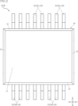
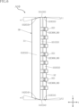
- FIG. 1 is a perspective view of a semiconductor device according to a first embodiment of the present disclosure.
- FIG. 2 is a plan view of the semiconductor device shown in FIG.
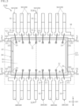
- FIG. 3 is a plan view corresponding to FIG. 2, showing the sealing resin through the plan view.
- FIG. 4 is a bottom view of the semiconductor device shown in FIG.
- FIG. 5 is a bottom view corresponding to FIG. 4, showing the sealing resin through the view.
- FIG. 6 is a front view of the semiconductor device shown in FIG. 7 is a right side view of the semiconductor device shown in FIG. 8 is a left side view of the semiconductor device shown in FIG.
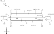
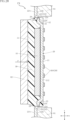
- FIG. 9 is a cross-sectional view taken along line IX-IX in FIG.
- FIG. 10 is a cross-sectional view taken along line XX in FIG.
- FIG. 10 is a cross-sectional view taken along line XX in FIG.
- FIG. 11 is a cross-sectional view taken along line XI-XI in FIG.
- FIG. 12 is a partially enlarged view of FIG.
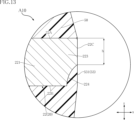
- FIG. 13 is a partially enlarged view of FIG.
- FIG. 14 is a partially enlarged cross-sectional view of a semiconductor device according to a modified example of the first embodiment of the present disclosure.
- 15A to 15C are cross-sectional views for explaining a manufacturing process of the semiconductor device shown in FIG. 16A to 16C are cross-sectional views for explaining a manufacturing process of the semiconductor device shown in FIG. 17A to 17C are cross-sectional views illustrating a manufacturing process of the semiconductor device shown in FIG. 18A to 18C are cross-sectional views for explaining a manufacturing process of the semiconductor device shown in FIG.
- FIG. 19A to 19C are cross-sectional views for explaining the manufacturing process of the semiconductor device shown in FIG. 20A to 20C are cross-sectional views for explaining the manufacturing process of the semiconductor device shown in FIG.
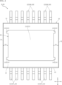
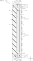
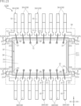
- FIG. 21 is a plan view of the semiconductor device according to the second embodiment of the present disclosure, showing the semiconductor device through a sealing resin.
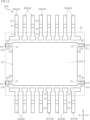
- FIG. 22 is a bottom view of the semiconductor device shown in FIG. 21, seen through the sealing resin.
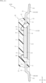
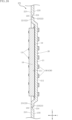
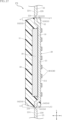
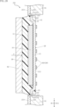
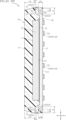
- FIG. 23 is a cross-sectional view taken along line XXIII-XXIII in FIG.
- FIG. 24 is a cross-sectional view taken along line XXIV-XXIV in FIG.
- FIG. 25 is a partially enlarged view of FIG.
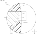
- FIG. 26 is a partially enlarged view of FIG. FIG.
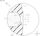
- FIG. 27 is a partially enlarged cross-sectional view of a semiconductor device according to a modified example of the second embodiment of the present disclosure.
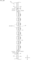
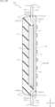
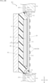
- 28A to 28C are cross-sectional views illustrating a manufacturing process of the semiconductor device shown in FIG. 29A to 29C are cross-sectional views illustrating a manufacturing process of the semiconductor device shown in FIG. 30 is a cross-sectional view illustrating a manufacturing process of the semiconductor device shown in FIG. 31A to 31C are cross-sectional views illustrating a manufacturing process of the semiconductor device shown in FIG.
- a semiconductor device A10 according to a first embodiment of the present disclosure will be described with reference to Figures 1 to 13.
- the semiconductor device A10 includes a semiconductor element 10, a first lead 20, a plurality of second leads 30, a plurality of wires 40, and a sealing resin 50.
- the package format of the semiconductor device A10 is a small outline package (SOP).
- SOP small outline package
- Figures 3 and 5 show the sealing resin 50 in a see-through manner for ease of understanding.
- the outline of the sealing resin 50 is shown by an imaginary line (two-dot chain line).
- the normal direction of the mounting surface 211 of the pad portion 21 described later is called the "first direction z”.
- the direction perpendicular to the first direction z is called the "second direction x”.
- the direction perpendicular to both the first direction z and the second direction x is called the "third direction y”.
- the sealing resin 50 covers the semiconductor element 10, a portion of the first lead 20, a portion of each of the multiple second leads 30, and the multiple wires 40.
- the sealing resin 50 is an insulator.
- the sealing resin 50 is made of a material that contains, for example, epoxy resin. When viewed in the first direction z, the sealing resin 50 is rectangular.
- the sealing resin 50 has a top surface 51, a bottom surface 52, a first side surface 53, a second side surface 54, and two third side surfaces 55.
- the top surface 51 faces one side in the first direction z.
- the top surface 51 faces the same side in the first direction z as the mounting surface 211 of the pad portion 21, which will be described later.
- the bottom surface 52 faces the opposite side to the top surface 51 in the first direction z.
- the first side surface 53 is connected to the top surface 51 and the bottom surface 52 and faces one side of the second direction x.
- the first side surface 53 includes a first region 531, a second region 532, and a third region 533.
- the first region 531 includes the first direction z as an in-plane direction. When viewed in the first direction z, the first region 531 is located outward from each of the top surface 51 and the bottom surface 52.
- the second region 532 is located between the first region 531 and the top surface 51 in the first direction z.
- the third region 533 is located on the opposite side to the second region 532 with respect to the first region 531.
- Each of the second region 532 and the third region 533 is inclined with respect to the first region 531.
- the inclination angle ⁇ 1 of the second region 532 with respect to the first region 531 is larger than the inclination angle ⁇ 1 of the third region 533 with respect to the first region 531.
- the second side 54 is connected to the top surface 51 and the bottom surface 52 and faces the opposite side to the first side 53 in the second direction x.
- the second side 54 includes a fourth region 541, a fifth region 542, and a sixth region 543.
- the fourth region 541 includes the first direction z as an in-plane direction. When viewed in the first direction z, the fourth region 541 is located outward from each of the top surface 51 and the bottom surface 52.
- the fifth region 542 is located between the fourth region 541 and the top surface 51 in the first direction z.
- the sixth region 543 is located on the opposite side to the fifth region 542 with respect to the fourth region 541.
- Each of the fifth region 542 and the sixth region 543 is inclined with respect to the fourth region 541.
- the inclination angle ⁇ 2 of the fifth region 542 with respect to the fourth region 541 is greater than the inclination angle ⁇ 2 of the sixth region 543 with respect to the fourth region 541.
- each of the two third side surfaces 55 is connected to the top surface 51 and the bottom surface 52 and faces opposite each other in the third direction y.
- Each of the two third side surfaces 55 includes a seventh region 551, an eighth region 552, and a ninth region 553.
- the seventh region 551 includes the first direction z as an in-plane direction. When viewed in the first direction z, the seventh region 551 is located outward from each of the top surface 51 and the bottom surface 52.
- the eighth region 552 is located between the seventh region 551 and the top surface 51 in the first direction z.
- the ninth region 553 is located on the opposite side to the eighth region 552 with respect to the seventh region 551.
- Each of the eighth region 552 and the ninth region 553 is inclined with respect to the seventh region 551.
- the inclination angle ⁇ 3 of the eighth region 552 relative to the seventh region 551 is equal to the inclination angle ⁇ 3 of the ninth region 553 relative to the seventh region 551.
- the first lead 20 and the multiple second leads 30 both contain copper (Cu).
- the first lead 20 and the multiple second leads 30 are obtained from the same lead frame.
- the first lead 20 carries the semiconductor element 10.
- the first lead 20 has a pad portion 21, a first support portion 22, a second support portion 23, a third support portion 24, and a fourth support portion 25.
- the pad portion 21 carries the semiconductor element 10.
- the first lead 20 is rectangular.
- the pad portion 21 has a mounting surface 211 and an exposed surface 212.
- the mounting surface 211 faces one side in the first direction z.
- the semiconductor element 10 is mounted on the mounting surface 211.
- the exposed surface 212 faces the opposite side to the mounting surface 211 in the first direction z.
- the exposed surface 212 is exposed from the bottom surface 52 of the sealing resin 50.
- the first support portion 22 is connected to one side of the pad portion 21 in the second direction x.
- the first support portion 22 is located closer to the first side surface 53 of the sealing resin 50 than the second side surface 54 of the sealing resin 50.
- the first support portion 22 has a first surface 22A, a second surface 22B and a first end surface 22C.
- the first surface 22A faces the same side as the mounting surface 211 in the first direction z.
- the second surface 22B faces the opposite side to the first surface 22A in the first direction z.
- the first surface 22A and the second surface 22B are covered by the sealing resin 50.
- the first end surface 22C faces one side in the second direction x.
- the first end surface 22C is exposed from a first region 531 of the first side surface 53.
- the dimension H2 in the first direction z of the sealing resin 50 from the bottom surface 52 of the sealing resin 50 to the second surface 22B is smaller than the dimension H1 in the first direction z of the sealing resin 50 from the top surface 51 of the sealing resin 50 to the first surface 22A.
- the dimension H2 is 50% or less of the dimension H1.
- the dimension L1 in the second direction x of the second surface 22B is adjacent to the exposed surface 212 of the pad portion 21 on one side of the second direction x and is 50% or more of the dimension D1 in the second direction x of the area of the bottom surface 52 that overlaps with the second surface 22B when viewed in the first direction z.
- the first support portion 22 has a first main portion 221, a first connecting portion 222 and a first end portion 223.
- the first main portion 221 includes a first surface 22A and a second surface 22B.
- the first connecting portion 222 is connected to the first main portion 221 and the pad portion 21.
- the first connecting portion 222 is inclined relative to the mounting surface 211 in the second direction x toward the side away from the pad portion 21.
- the inclination angle ⁇ 1 of the first connecting portion 222 relative to the mounting surface 211 is preferably 50° or less.
- the first end portion 223 is located on the opposite side of the first connecting portion 222 with respect to the first main portion 221 in the second direction x, and is connected to the first main portion 221.
- the first end portion 223 includes a first surface 22A, a second surface 22B and a first end surface 22C.
- the first end 223 of the first support portion 22 has a first recessed portion 224 recessed from the second surface 22B.
- the first recessed portion 224 is connected to the first main portion 221 and the first end surface 22C.
- the semiconductor device A10 by providing the first recessed portion 224 at the first end 223, the cross-sectional area of the first end 223 along a direction perpendicular to the second direction x is reduced from the first main portion 221 to the first end surface 22C.
- the first recess 224 of the first end portion 223 is in contact with the sealing resin 50.
- the dimension of the first recess 224 in the second direction x is smaller than the dimension L1 of the second surface 22B of the first support portion 22.
- the first end surface 22C is flush with the first region 531 of the first side surface 53 of the sealing resin 50.
- the dimension b of the first end face 22C in the third direction y is different from the dimension h of the first end face 22C in the first direction z.
- the dimension h is smaller than the dimension b.
- the second support portion 23 is located on the opposite side of the first support portion 22 with respect to the pad portion 21 in the second direction x, and is connected to the pad portion 21.
- the second support portion 23 is located closer to the second side surface 54 of the sealing resin 50 than the first side surface 53 of the sealing resin 50.
- the second support portion 23 has a third surface 23A, a fourth surface 23B and a second end surface 23C.
- the third surface 23A faces the same side as the mounting surface 211 in the first direction z.
- the fourth surface 23B faces the opposite side to the third surface 23A in the first direction z.
- the third surface 23A and the fourth surface 23B are covered by the sealing resin 50.
- the second end surface 23C faces the opposite side to the first end surface 22C of the first support portion 22 in the second direction x.
- the second end surface 23C is exposed from the fourth region 541 of the second side surface 54.
- the dimension H4 in the first direction z of the sealing resin 50 from the bottom surface 52 of the sealing resin 50 to the fourth surface 23B is smaller than the dimension H3 in the first direction z of the sealing resin 50 from the top surface 51 of the sealing resin 50 to the third surface 23A.
- the dimension H4 is 50% or less of the dimension H3.
- the dimension L2 in the second direction x of the fourth surface 23B is adjacent to the exposed surface 212 of the pad portion 21 on one side of the second direction x and is 50% or more of the dimension D2 in the second direction x of the area of the bottom surface 52 that overlaps with the fourth surface 23B when viewed in the first direction z.
- the second support portion 23 has a second main portion 231, a second connecting portion 232 and a second end portion 233.
- the second main portion 231 includes a third surface 23A and a fourth surface 23B.
- the second connecting portion 232 is connected to the second main portion 231 and the pad portion 21.
- the second connecting portion 232 is inclined with respect to the mounting surface 211 toward the side away from the pad portion 21 in the second direction x.
- the inclination angle ⁇ 2 of the second connecting portion 232 with respect to the mounting surface 211 is preferably 50° or less.
- the second end portion 233 is located on the opposite side of the second main portion 231 from the second connecting portion 232 in the second direction x, and is connected to the second main portion 231.
- the second end portion 233 includes a third surface 23A, a fourth surface 23B and a second end surface 23C.
- the second end 233 of the second support portion 23 has a second recessed portion 234 recessed from the fourth surface 23B.
- the second recessed portion 234 is connected to the second main portion 231 and the second end surface 23C.
- the cross-sectional area of the second end 233 along a direction perpendicular to the second direction x is reduced from the second main portion 231 to the second end surface 23C.
- the dimension of the pad portion 21 in the second direction x is at least 10 times the dimension of each of the first support portion 22 and the second support portion 23 in the second direction x.
- the third support portion 24 is located on the same side as the first support portion 22 with respect to the pad portion 21 in the second direction x, and is connected to the pad portion 21.
- the third support portion 24 is separated from the first support portion 22 in the third direction y.
- the third support portion 24 has a fifth surface 24A, a sixth surface 24B and a third end surface 24C.
- the fifth surface 24A faces the same side as the mounting surface 211 in the first direction z.
- the sixth surface 24B faces the opposite side to the fifth surface 24A in the first direction z.
- the fifth surface 24A and the sixth surface 24B are covered with the sealing resin 50.
- the third end surface 24C faces the same side as the first end surface 22C of the first support portion 22 in the second direction x.
- the third end surface 24C is exposed from the first region 531 of the first side surface 53 of the sealing resin 50.
- the dimension H6 in the first direction z of the sealing resin 50 from the bottom surface 52 of the sealing resin 50 to the sixth surface 24B is smaller than the dimension H5 in the first direction z of the sealing resin 50 from the top surface 51 of the sealing resin 50 to the fifth surface 24A.
- it is preferable that the dimension H6 is 50% or less of the dimension H5.
- the dimension L3 in the second direction x of the sixth surface 24B is adjacent to the exposed surface 212 of the pad portion 21 on one side of the second direction x and is 50% or more of the dimension D1 in the second direction x of the area of the bottom surface 52 that overlaps with the sixth surface 24B when viewed in the first direction z.
- the third support portion 24 has a third main portion 241, a third connecting portion 242 and a third end portion 243.
- the third main portion 241 includes a fifth surface 24A and a sixth surface 24B.
- the third connecting portion 242 is connected to the third main portion 241 and the pad portion 21.
- the third connecting portion 242 is inclined relative to the mounting surface 211 toward the side away from the pad portion 21 in the second direction x.
- the inclination angle ⁇ 3 of the third connecting portion 242 relative to the mounting surface 211 is preferably 50° or less.
- the third end portion 243 is located on the opposite side of the third connecting portion 242 with respect to the third main portion 241 in the second direction x, and is connected to the third main portion 241.
- the third end portion 243 includes a fifth surface 24A, a sixth surface 24B and a third end surface 24C.
- the third end 243 of the third support portion 24 has a third recessed portion 244 recessed from the sixth surface 24B.
- the third recessed portion 244 is connected to the third main portion 241 and the third end surface 24C.
- the cross-sectional area of the third end 243 along a direction perpendicular to the second direction x is reduced from the third main portion 241 to the third end surface 24C.
- the fourth support portion 25 is located on the same side as the second support portion 23 with respect to the pad portion 21 in the second direction x, and is connected to the pad portion 21.
- the fourth support portion 25 is separated from the second support portion 23 in the third direction y.
- the fourth support portion 25 has a seventh surface 25A, an eighth surface 25B and a fourth end surface 25C.
- the seventh surface 25A faces the same side as the mounting surface 211 in the first direction z.
- the eighth surface 25B faces the opposite side to the seventh surface 25A in the first direction z.
- the seventh surface 25A and the eighth surface 25B are covered with the sealing resin 50.
- the fourth end surface 25C faces the same side as the second end surface 23C of the second support portion 23 in the second direction x.
- the fourth end surface 25C is exposed from the fourth region 541 of the second side surface 54 of the sealing resin 50.
- the dimension H8 in the first direction z of the sealing resin 50 from the bottom surface 52 of the sealing resin 50 to the eighth surface 25B is smaller than the dimension H7 in the first direction z of the sealing resin 50 from the top surface 51 of the sealing resin 50 to the seventh surface 25A.
- the dimension H8 is 50% or less of the dimension H7.
- the dimension L4 in the second direction x of the eighth surface 25B is adjacent to the exposed surface 212 of the pad portion 21 on one side of the second direction x and is 50% or more of the dimension D2 in the second direction x of the area of the bottom surface 52 that overlaps with the eighth surface 25B when viewed in the first direction z.
- the fourth support portion 25 has a fourth main portion 251, a fourth connecting portion 252 and a fourth end portion 253.
- the fourth main portion 251 includes a seventh surface 25A and an eighth surface 25B.
- the fourth connecting portion 252 is connected to the fourth main portion 251 and the pad portion 21.
- the fourth connecting portion 252 is inclined with respect to the mounting surface 211 toward the side away from the pad portion 21 in the second direction x.
- the inclination angle ⁇ 4 of the fourth connecting portion 252 with respect to the mounting surface 211 is preferably 50° or less.
- the fourth end portion 253 is located on the opposite side of the fourth connecting portion 252 with respect to the fourth main portion 251 in the second direction x, and is connected to the fourth main portion 251.
- the fourth end portion 253 includes a seventh surface 25A, an eighth surface 25B and a fourth end surface 25C.
- the fourth end 253 of the fourth support portion 25 has a fourth recessed portion 254 recessed from the eighth surface 25B.
- the fourth recessed portion 254 is connected to the fourth main portion 251 and the fourth end surface 25C.
- the cross-sectional area of the fourth end 253 along a direction perpendicular to the second direction x is reduced from the fourth main portion 251 to the fourth end surface 25C.
- the semiconductor element 10 is mounted on the pad portion 21 of the first lead 20.
- the semiconductor element 10 controls the functions of the semiconductor device A10.
- the type of the semiconductor element 10 is not limited, and may be an IC or an LSI.
- the semiconductor element 10 is bonded to the mounting surface 211 of the pad portion 21 via a bonding layer 19.
- the bonding layer 19 is made of a paste containing metal particles.
- the metal particles are, for example, silver (Ag). Therefore, the bonding layer 19 is a conductor. Alternatively, the bonding layer 19 may be solder.
- the semiconductor element 10 has an element surface 11 and a plurality of electrodes 12.
- the element surface 11 faces the same side as the mounting surface 211 of the pad portion 21 in the first direction z.
- the element surface 11 is located between the top surface 51 of the sealing resin 50 and the first surface 22A of the first support portion 22, the third surface 23A of the second support portion 23, the fifth surface 24A of the third support portion 24, and the seventh surface 25A of the fourth support portion 25 in the first direction z.
- the semiconductor element 10 when viewed in a direction perpendicular to the first direction z, the semiconductor element 10 includes portions protruding in the first direction z from each of the first support portion 22, the second support portion 23, the third support portion 24, and the fourth support portion 25.
- the plurality of electrodes 12 are provided on the element surface 11. Each of the plurality of electrodes 12 is electrically connected to a circuit configured in the semiconductor element 10.
- the multiple second leads 30 are arranged on both sides of the first lead 20 in the third direction y. Each of the multiple second leads 30 is electrically connected to the semiconductor element 10.
- the multiple second leads 30 include multiple first terminals 30A and multiple second terminals 30B.
- the multiple first terminals 30A are located on one side of the first lead 20 in the third direction y.
- the multiple first terminals 30A are arranged along the second direction x. Each of the multiple first terminals 30A protrudes from the seventh region 551 of one of the two third side surfaces 55 of the sealing resin 50.
- the multiple second terminals 30B are located on the opposite side of the multiple first terminals 30A with respect to the first lead 20 in the third direction y.
- the multiple second terminals 30B are arranged along the second direction x. Each of the multiple second terminals 30B protrudes from the seventh region 551 of the other of the two third side surfaces 55.
- each of the multiple second leads 30 has an inner portion 31 and an outer portion 32.
- the inner portion 31 is covered with sealing resin 50.
- the inner portion 31 of each of the multiple second leads 30 has a connection surface 311.
- the connection surface 311 faces the same side as the mounting surface 211 of the pad portion 21 in the first direction z.
- the connection surface 311 is located between the mounting surface 211 and the top surface 51 of the sealing resin 50 in the first direction z.
- the connection surface 311 is located between the mounting surface 211 and the element surface 11 of the semiconductor element 10 in the first direction z.
- connection surface 311 of each of the multiple second leads 30, the first surface 22A of the first support portion 22, the third surface 23A of the second support portion 23, the fifth surface 24A of the third support portion 24, and the seventh surface 25A of the fourth support portion 25 are all included in the same plane.
- the outer part 32 is connected to the inner part 31 of one of the corresponding second leads 30.
- the outer part 32 protrudes from the seventh region 551 of one of the two third side surfaces 55 of the sealing resin 50.
- the surface of the outer part 32 is plated with tin, for example.
- the outer part 32 extends in the third direction y.
- the outer part 32 is bent in a gull-wing shape.
- the outer part 32 of each of the multiple second leads 30 has a mounting surface 321.
- the mounting surface 321 is exposed from the sealing resin 50.
- the mounting surface 321 faces the opposite side to the connection surface 311 of the corresponding inner part 31 and is located furthest from the connection surface 311 of the corresponding inner part 31.
- the mounting surface 321 protrudes from within a plane that includes the bottom surface 52 of the sealing resin 50.
- the mounting surface 321 is inclined with respect to the bottom surface 52.
- each of the multiple wires 40 is individually conductively bonded to the multiple electrodes 12 of the semiconductor element 10 and to the connection surfaces 311 of each of the multiple second leads 30. As a result, each of the multiple second leads 30 is electrically connected to the semiconductor element 10.
- the multiple wires 40 contain, for example, gold (Au). Alternatively, the multiple wires 40 may contain aluminum (Al) or copper.
- FIG. 14 corresponds to FIG. 13 showing the semiconductor device A10.
- the configuration of the first support portion 22 of the first lead 20 differs from that of the semiconductor device A10.
- the first end 223 is located between the first surface 22A and the first end surface 22C in the second direction x, and has a first intermediate surface 223A connected to the first surface 22A.
- the first intermediate surface 223A overlaps the first main portion 221.
- the first end surface 22C is located between the first intermediate surface 223A and the second recess 234 in the first direction z.
- the dimension of the first intermediate surface 223A in the second direction x is larger than the dimension of the second recess 234 in the second direction x.
- the first intermediate surface 223A is inclined toward the inside of the first end 223 in the first direction z with respect to the first surface 22A, and is also connected to the first end surface 22C.
- the first intermediate surface 223A is covered with a sealing resin 50.
- Figures 15 to 18 correspond to Figure 9, which shows semiconductor device A10.
- a first process P1 is performed to form a first lead 20 having a pad portion 21, a first support portion 22 and a second support portion 23.
- the first process P1 is performed in conjunction with the formation of a lead frame including the first lead 20 and a plurality of second leads 30.
- the description of the formation of the third support portion 24 and the fourth support portion 25 of the first lead 20 is omitted.
- a first recessed portion 224 is formed in the first end portion 223 of the first support portion 22, thereby reducing the cross-sectional area of the first end portion 223 along a direction perpendicular to the second direction x from the first main portion 221 of the first support portion 22 to the first end face 22C. Additionally, by forming the second recess 234 at the second end 233 of the second support part 23, the cross-sectional area of the second end 233 along a direction perpendicular to the second direction x is reduced from the second main part 231 of the second support part 23 to the second end surface 23C.
- a second process P2 is performed in which the semiconductor element 10 is bonded to the mounting surface 211 of the pad portion 21.
- the semiconductor element 10 is bonded to the mounting surface 211 via the bonding layer 19.
- a plurality of wires 40 are formed by wire bonding, which are individually conductively bonded to the plurality of electrodes 12 of the semiconductor element 10 and the respective connection surfaces 311 of the plurality of second leads 30.
- the third process P3 is performed to form the sealing resin 50 that covers the pad portion 21, parts of the first support portion 22, and parts of the second support portion 23, and the semiconductor element 10.
- the sealing resin 50 is formed by transfer molding.
- parts of the first surface 22A and the second surface 22B of the first support portion 22, and parts of the third surface 23A and the fourth surface 23B of the second support portion 23 are covered with the sealing resin 50.
- at least a part of the first recess 224 formed in the first support portion 22 and at least a part of the second recess 234 formed in the second support portion 23 are covered with the sealing resin 50.
- the exposed surface 212 of the pad portion 21 is exposed from the bottom surface 52.
- the dimension H2 shown in FIG. 9 is made smaller than the dimension H1.
- the dimension H4 shown in FIG. 9 is made smaller than the dimension H3.
- the first support portion 22 is protruded from the first region 531 of the first side surface 53 of the sealing resin 50.
- the inclination angle ⁇ 1 of the second region 532 of the first side surface 53 relative to the first region 531 is made larger than the inclination angle ⁇ 1 of the third region 533 of the first side surface 53 relative to the first region 531.
- the second support portion 23 is protruded from the fourth region 541 of the second side surface 54 of the sealing resin 50.
- the inclination angle ⁇ 2 of the fifth region 542 of the second side surface 54 relative to the fourth region 541 is made larger than the inclination angle ⁇ 2 of the sixth region 543 of the second side surface 54 relative to the fourth region 541.
- a fourth step P4 is performed to cut each of the first support portion 22 and the second support portion 23.
- the second surface 22B of the first support portion 22 and the fourth surface 23B of the second support portion 23 are supported by the support body 81.
- a compressive force P is applied to the top surface 51 of the sealing resin 50 by the load body 82, thereby cutting each of the first support portion 22 and the second support portion 23.
- a first end surface 22C corresponding to the cut surface of the first support portion 22 is formed at the first end portion 223.
- a second end surface 23C corresponding to the cut surface of the second support portion 23 is formed at the second end portion 233.
- the first support portion 22 is cut starting from the first recessed portion 224.
- the second support portion 23 is cut starting from the second recessed portion 234.
- Figures 19 and 20 correspond to Figure 9 showing semiconductor device A10.
- grooves 29 recessed from the first surface 22A of the first support portion 22 and the third surface 23A of the second support portion 23 are formed in the first support portion 22 and the second support portion 23.
- the grooves 29 formed in the first support portion 22 overlap the first recessed portion 224.
- the grooves 29 formed in the second support portion 23 overlap the second recessed portion 234.
- the second process P2 and the third process P3 in the manufacture of the semiconductor device A11 are similar to those in the manufacture of the semiconductor device A10, and therefore will not be described here.
- the first support portion 22 is cut starting from both the first recessed portion 224 and the groove portion 29.
- the second support portion 23 is cut starting from both the second recessed portion 234 and the groove portion 29.
- a portion of the inner circumferential surface 291 that defines the groove portion 29 corresponds to the first intermediate surface 223A of the first end portion 223.
- the manufacturing method of the semiconductor device A10 includes a first process P1 of forming a first lead 20 having a pad portion 21 and a first support portion 22, a second process P2 of joining a semiconductor element 10 to the pad portion 21, a third process P3 of forming a sealing resin 50, and a fourth process P4 of cutting the first support portion 22.
- the pad portion 21 is exposed from the bottom surface 52 of the sealing resin 50.
- the dimension H2 in the first direction z of the sealing resin 50 from the bottom surface 52 to the second surface 22B of the first support portion 22 is made smaller than the dimension H1 in the first direction z of the sealing resin 50 from the top surface 51 of the sealing resin 50 to the first surface 22A of the first support portion 22.
- the second surface 22B is supported by the support 81, and then a compressive force P is applied to the top surface 51 to cut the first support portion 22.
- the first support 22 is formed with a first end surface 22C that faces one side of the second direction x and is exposed from the sealing resin 50.
- the cross-sectional area of the first end 223 of the first support portion 22 along a direction perpendicular to the second direction x is reduced from the first main portion 221 to the first end face 22C.
- the area of the first end face 22C is reduced, which makes it easier to cut the first support portion 22 in the fourth step P4 shown in FIG. 18.
- a first recess 224 recessed from the second surface 22B is formed in the first support 22 including the first end 223.
- the first recess 224 is connected to the first main portion 221.
- the first support 22 is cut starting from the first recess 224 while a compressive force P is applied to the top surface 51 of the sealing resin 50, so that the cutting of the first support 22 becomes smoother.
- the dimension h in the first direction z of the first end surface 22C of the first support 22 can be made smaller than the dimension b in the third direction y of the first end surface 22C. This further reduces the second moment of area around the third direction y of the first end surface 22C.
- the first connecting portion 222 of the first support portion 22 is inclined relative to the mounting surface 211 in the second direction x away from the pad portion 21.
- the inclination angle ⁇ 1 of the second region 532 of the first side surface 53 relative to the first region 531 of the first side surface 53 is greater than the inclination angle ⁇ 1 of the third region 533 of the first side surface 53 relative to the first region 531.
- FIG. 21 shows the sealing resin 50 in a see-through manner for ease of understanding.
- the outline of the sealing resin 50 is shown by imaginary lines.
- semiconductor device A20 the configurations of the first support portion 22, the second support portion 23, the third support portion 24, and the fourth support portion 25 of the first lead 20 differ from those of semiconductor device A10.
- the first end 223 has two first recesses 224 that are individually recessed from both sides in the third direction y.
- Each of the two first recesses 224 is connected to the periphery of the first surface 22A of the first end 223 and the periphery of the second surface 22B of the first end 223.
- the second end 233 has two second recesses 234 that are individually recessed from both sides in the third direction y.
- Each of the two second recesses 234 is connected to the periphery of the third surface 23A of the second end 233 and the periphery of the fourth surface 23B of the second end 233.
- the third end 243 has two third recesses 244 that are individually recessed from both sides in the third direction y.
- Each of the two third recesses 244 is connected to the periphery of the fifth surface 24A of the third end 243 and the periphery of the sixth surface 24B of the third end 243.
- the fourth end 253 has two fourth recesses 254 that are individually recessed from both sides in the third direction y.
- Each of the two fourth recesses 254 is connected to the periphery of the seventh surface 25A of the fourth end 253 and the periphery of the eighth surface 25B of the fourth end 253.
- the first end 223 is located between the second surface 22B and the first end surface 22C in the second direction x, and has a first intermediate surface 223A connected to the second surface 22B.
- the first intermediate surface 223A overlaps the first main portion 221.
- the first end surface 22C is located between the first intermediate surface 223A and the first surface 22A in the first direction z.
- the dimension of the first intermediate surface 223A in the second direction x is smaller than the dimension L1 of the second surface 22B of the first end 223.
- the first intermediate surface 223A is inclined toward the inside of the first end 223 in the first direction z with respect to the second surface 22B, and is also connected to the first end surface 22C.
- the first intermediate surface 223A is covered with sealing resin 50.
- the first end surface 22C is away from the first region 531 of the first side surface 53 of the sealing resin 50 on the side where the pad portion 21 is located in the second direction x.
- FIG. 27 corresponds to FIG. 26 showing the semiconductor device A20.
- the configuration of the first support portion 22 of the first lead 20 differs from that of the semiconductor device A20.
- the first end 223 is located between the first surface 22A and the first end surface 22C in the second direction x, and has a second intermediate surface 223B connected to the first surface 22A.
- the second intermediate surface 223B overlaps the first main portion 221.
- the first end surface 22C is located between the first intermediate surface 223A and the second intermediate surface 223B in the first direction z.
- the dimension of the second intermediate surface 223B in the second direction x is smaller than the dimension of the first surface 22A of the first end 223 in the second direction x.
- the second intermediate surface 223B is inclined toward the inside of the first end 223 in the first direction z with respect to the first surface 22A, and is also connected to the first end surface 22C.
- the second intermediate surface 223B is covered with a sealing resin 50.
- Figures 28 to 30 correspond to Figure 23, which shows semiconductor device A20.
- a first step P1 is performed to form a first lead 20 having a pad portion 21, a first support portion 22, and a second support portion 23.
- two first recesses 224 are formed in the first end portion 223 of the first support portion 22, thereby reducing the cross-sectional area of the first end portion 223 along a direction perpendicular to the second direction x from the first main portion 221 to the first end surface 22C of the first support portion 22.
- two second recesses 234 are formed in the second end portion 233 of the second support portion 23, thereby reducing the cross-sectional area of the second end portion 233 along a direction perpendicular to the second direction x from the second main portion 231 to the second end surface 23C of the second support portion 23.
- grooves 29 recessed from the second surface 22B of the first support portion 22 and the fourth surface 23B of the second support portion 23 are formed in the first support portion 22 and the second support portion 23.
- the grooves 29 extend in the third direction y.
- the grooves 29 are defined by an inner circumferential surface 291 that is connected to either the second surface 22B or the fourth surface 23B.
- the grooves 29 formed in the first support portion 22 are positioned on the opposite side of the first main portion 221 with respect to the two first recesses 224 in the second direction x.
- the grooves 29 formed in the second support portion 23 are positioned on the opposite side of the second main portion 231 with respect to the two second recesses 234 in the second direction x.
- a second process P2 is performed in which the semiconductor element 10 is bonded to the mounting surface 211 of the pad portion 21.
- the second process P2 is similar to the second process P2 in the manufacture of the semiconductor device A10 shown in FIG. 16, and therefore a description thereof will be omitted here.
- a third process P3 is performed to form sealing resin 50 that covers parts of pad portion 21, first support portion 22, and second support portion 23, and semiconductor element 10.
- sealing resin 50 that covers parts of pad portion 21, first support portion 22, and second support portion 23, and semiconductor element 10.
- groove portions 29 formed in first support portion 22 and second support portion 23 are covered with sealing resin.
- a fourth process P4 is performed in which the first support portion 22 and the second support portion 23 are each cut.
- the first support portion 22 and the second support portion 23 are each cut starting from the groove portion 29.
- a portion of the inner circumferential surface 291 that defines the groove portion 29 corresponds to the first intermediate surface 223A of the first end portion 223.
- FIG. 31 corresponds to FIG. 23 showing semiconductor device A20.
- grooves 29 recessed from the first surface 22A and the second surface 22B of the first support portion 22 and the third surface 23A and the fourth surface 23B of the second support portion 23 are formed in the first support portion 22 and the second support portion 23.
- the grooves 29 formed in the second surface 22B of the first support portion 22 overlap the grooves 29 formed in the first surface 22A of the first support portion 22.
- the grooves 29 formed in the fourth surface 23B of the second support portion 23 overlap the grooves 29 formed in the third surface 23A of the second support portion 23.
- the second process P2, the third process P3, and the fourth process P4 in the manufacture of the semiconductor device A21 are similar to those in the manufacture of the semiconductor device A20, and therefore will not be described here.
- the manufacturing method of the semiconductor device A20 includes a first process P1 of forming a first lead 20 having a pad portion 21 and a first support portion 22, a second process P2 of joining a semiconductor element 10 to the pad portion 21, a third process P3 of forming a sealing resin 50, and a fourth process P4 of cutting the first support portion 22.
- the pad portion 21 is exposed from the bottom surface 52 of the sealing resin 50.
- the dimension H2 in the first direction z of the sealing resin 50 from the bottom surface 52 to the second surface 22B of the first support portion 22 is made smaller than the dimension H1 in the first direction z of the sealing resin 50 from the top surface 51 of the sealing resin 50 to the first surface 22A of the first support portion 22.
- the second surface 22B is supported by the support 81, and then a compressive force P is applied to the top surface 51 to cut the first support portion 22.
- the first support portion 22 is formed with a first end surface 22C that faces one side of the second direction x and is exposed from the sealing resin 50. Therefore, with this configuration, even during the manufacture of the semiconductor device A20, it is possible to reduce the stress concentration in the sealing resin 50 that occurs when the first lead 20 is cut.
- the manufacturing method for the semiconductor device A20 has a configuration in common with the manufacturing method for the semiconductor device A10, thereby achieving the same effects as the manufacturing method for the semiconductor device A10.
- the first end 223 of the first support portion 22 has a first intermediate surface 223A.
- the first intermediate surface 223A overlaps with the first main portion 221.
- the first end surface 22C of the first support portion 22 is located between the first intermediate surface 223A and the first surface 22A in the first direction z.
- the first intermediate surface 223A corresponds to a part of the inner circumferential surface 291 that defines the groove portion 29 formed in the first step P1.
- Appendix 1 a first step of forming a first lead having a pad portion having a mounting surface facing one side in a first direction and a first support portion connected to one side of the pad portion in a second direction perpendicular to the first direction; a second step of bonding a semiconductor element to the mounting surface; a third step of forming a sealing resin that covers the pad portion, a portion of the first support portion, and the semiconductor element; and a fourth step of cutting the first support portion, the sealing resin has a top surface facing the same side as the mounting surface in the first direction and a bottom surface facing an opposite side to the top surface in the first direction, the first support portion has a first surface facing the same side as the mounting surface in the first direction, and a second surface facing an opposite side to the first surface in the first direction, In the third step, the sealing resin is formed so that a portion of each of the first surface and the second surface is covered with the sealing resin, the pad portion is exposed from the bottom surface,
- Appendix 2. The method for manufacturing a semiconductor device described in Appendix 1, wherein in the third step, the sealing resin is formed so that a dimension of the sealing resin in the first direction from the bottom surface to the second surface is 50% or less of a dimension of the sealing resin in the first direction from the top surface to the first surface.
- the first support portion has a first main portion including the first surface and the second surface, each of which is covered with the sealing resin, a first connecting portion connecting the first main portion and the pad portion, and a first end portion located on the opposite side of the first connecting portion with respect to the first main portion in the second direction and connected to the first main portion; the first end portion includes the first surface covered with the sealing resin and the first end surface formed in the fourth step, 2.
- a recess recessed from the second surface is formed in the first support portion including the first end portion, 6.
- a groove portion recessed from the first surface and extending in the third direction is formed in the first support portion, When viewed in the first direction, the groove portion overlaps the recessed portion, 7.
- the first support portion has an inner circumferential surface that defines the groove portion, 8.
- the first end face is connected to an outer edge of the inner circumferential surface.
- a recessed portion recessed from one side in the third direction is formed in the first support portion including the first end portion, 5.
- the method for manufacturing a semiconductor device according to claim 4, wherein the recess is connected to a peripheral edge of the first surface. Appendix 10.
- a groove portion recessed from the first surface and extending in the third direction is formed in the first support portion, the groove portion is located on an opposite side of the recessed portion from the first main portion in the second direction, 10.
- Appendix 12. 12.
- the method for manufacturing a semiconductor device according to claim 11, wherein an inclination angle of the first connecting portion with respect to the mounting surface is 50° or less. Appendix 13.
- the first lead has a second support portion located on an opposite side of the first support portion with respect to the pad portion in the second direction and connected to the pad portion;
- the second support portion has a third surface facing the same side as the mounting surface in the first direction, and a fourth surface facing an opposite side to the third surface in the first direction
- in the third step a portion of each of the third surface and the fourth surface is covered with the sealing resin, and the sealing resin is formed such that a dimension of the sealing resin from the bottom surface to the fourth surface in the first direction is smaller than a dimension of the sealing resin from the top surface to the third surface in the first direction;
- the fourth surface is supported by the support body, and a load is applied to the top surface, thereby cutting the second support portion; 12.
- a second end surface is formed on the second support portion, facing opposite the first end surface in the second direction and exposed from the sealing resin.
- the sealing resin has a first side surface facing the same side as the first end surface in the second direction; the first side surface includes a first region including the first direction as an in-plane direction, a second region located between the first region and the top surface in the first direction, and a third region located on the opposite side of the second region with respect to the first region;
- each of the second region and the third region is inclined with respect to the first region; 14.
- Appendix 15. The method for manufacturing a semiconductor device according to claim 14, wherein in the third step, the sealing resin is formed so that an inclination angle of the second region relative to the first region is larger than an inclination angle of the third region relative to the first region. Appendix 16.
- a first lead including a pad portion having a mounting surface facing one side in a first direction and a first support portion connected to one side of the pad portion in a second direction perpendicular to the first direction; a semiconductor element bonded to the mounting surface; a sealing resin that covers a portion of the first lead and the semiconductor element, the sealing resin has a top surface facing the same side as the mounting surface in the first direction, and a bottom surface facing an opposite side to the top surface in the first direction and from which the pad portion is exposed, the first support portion has a first surface facing the same side as the top surface in the first direction and covered with the sealing resin, a second surface facing an opposite side to the first surface in the first direction and covered with the sealing resin, and a first end surface facing the second direction and exposed from the sealing resin, a dimension of the sealing resin from the bottom surface to the second surface in the first direction is smaller than a dimension of the sealing resin from the top surface to the first surface in the first direction,
- a semiconductor device wherein a cross-sectional area of the first support
- a dimension of the first end surface in the first direction is smaller than a dimension of the first end surface in a third direction perpendicular to each of the first direction and the second direction;
- the first support portion is provided with a recessed portion recessed from the second surface, 17.
Landscapes
- Structures Or Materials For Encapsulating Or Coating Semiconductor Devices Or Solid State Devices (AREA)
Abstract
半導体装置の製造方法は、第1工程、第2工程、第3工程および第4工程を備える。前記第3工程では、封止樹脂の底面からパッド部を露出させる。前記第3工程では、前記底面から第1支持部の第2面に至る前記封止樹脂の第1方向の寸法を、前記封止樹脂の頂面から前記第1支持部の第1面に至る前記封止樹脂の前記第1方向の寸法よりも小さくする。前記第4工程では、前記第2面を支持体に支持させた上で前記頂面に圧縮力を載荷させることにより前記第1支持部が切断される。前記第4工程では、前記第1支持部には、第2方向の一方側を向き、かつ前記封止樹脂から露出する第1端面が形成される。
Description
本開示は、半導体装置の製造方法と、当該製造方法により得られる半導体装置とに関する。
特許文献1に開示されている半導体装置のように、樹脂パッケージ形式の半導体装置が広く知られている。特許文献1に開示されている半導体装置は、半導体素子と、当該半導体素子に導通する第1リードと、当該半導体素子を搭載する第2リードと、当該半導体素子を覆う封止樹脂とを備える。第1リードおよび第2リードの各々は、封止樹脂から突出している。
特許文献1に開示されている半導体装置の第2リードは、半導体素子が搭載される第2パッド部を有する。第2パッド部には、突起が設けられている。突起は、半導体素子に対向する第2パッド表面の法線方向に対して直交する方向に突出している。ここで、半導体装置の構成においては、リードフレームと第2リードとを連結する支持部材として、第2パッド部に設けられた突起を利用することがある。この場合の半導体装置の製造においては、封止樹脂を形成した後にリードフレームから突起を切り離す必要がある。この際、突起を含めた第2リードに荷重が作用するため、第2リードに接触する封止樹脂の部位により大きな応力が集中する。これにより、封止樹脂に亀裂が発生するおそれがある。
[概要]
本開示は、従来より改良が施された半導体装置を提供することを一の課題とする。特に本開示は、先述の事情に鑑み、装置製造の際、リードの切断に伴って作用する封止樹脂の応力集中を低減することが可能な半導体装置を提供することをその一の課題とする。
本開示は、従来より改良が施された半導体装置を提供することを一の課題とする。特に本開示は、先述の事情に鑑み、装置製造の際、リードの切断に伴って作用する封止樹脂の応力集中を低減することが可能な半導体装置を提供することをその一の課題とする。
本開示の第1の側面によって提供される半導体装置の製造方法は、第1方向の一方側を向く搭載面を有するパッド部と、前記パッド部の前記第1方向に対して直交する第2方向の一方側につながる第1支持部と、を有する第1リードを形成する第1工程と、前記搭載面に半導体素子を接合する第2工程と、前記パッド部および前記第1支持部の各々の一部、および前記半導体素子を覆う封止樹脂を形成する第3工程と、前記第1支持部を切断する第4工程とを備える。前記封止樹脂は、前記第1方向において前記搭載面と同じ側を向く頂面と、前記第1方向において前記頂面とは反対側を向く底面とを有する。前記第1支持部は、前記第1方向において前記搭載面と同じ側を向く第1面と、前記第1方向において前記第1面とは反対側を向く第2面とを有する。前記第3工程では、前記第1面および前記第2面の各々の一部が前記封止樹脂に覆われ、かつ前記底面から前記パッド部を露出させるとともに、前記底面から前記第2面に至る前記封止樹脂の前記第1方向の寸法が、前記頂面から前記第1面に至る前記封止樹脂の前記第1方向の寸法よりも小さくなるように前記封止樹脂が形成される。前記第4工程では、前記第2面を支持体に支持させた上で前記頂面に圧縮力を載荷させることにより前記第1支持部が切断される。前記第4工程では、前記第1支持部には、前記第2方向の一方側を向き、かつ前記封止樹脂から露出する第1端面が形成される。
本開示の第2の側面によって提供される半導体装置は、第1方向の一方側を向く搭載面を有するパッド部と、前記パッド部の前記第1方向に対して直交する第2方向の一方側につながる第1支持部とを有する第1リードと、前記搭載面に接合された半導体素子と、前記第1リードの一部、および前記半導体素子を覆う封止樹脂とを備える。前記封止樹脂は、前記第1方向において前記搭載面と同じ側を向く頂面と、前記第1方向において前記頂面とは反対側を向くとともに、前記パッド部が露出する底面とを有する。前記第1支持部は、前記第1方向において前記頂面と同じ側を向き、かつ前記封止樹脂に覆われた第1面と、前記第1方向において前記第1面とは反対側を向き、かつ前記封止樹脂に覆われた第2面と、前記第2方向を向き、かつ前記封止樹脂から露出する第1端面とを有する。前記底面から前記第2面に至る前記封止樹脂の前記第1方向の寸法は、前記頂面から前記第1面に至る前記封止樹脂の前記第1方向の寸法よりも小さい。前記第1支持部の前記第2方向に対して直交する方向に沿った断面積は、前記パッド部が位置する側から前記第1端面にかけて縮小している。
本開示のその他の特徴および利点は、添付図面に基づき以下に行う詳細な説明によって、より明らかとなろう。
[詳細な説明]
本開示の詳細について、添付図面に基づき説明する。
本開示の詳細について、添付図面に基づき説明する。
第1実施形態:
図1~図13に基づき、本開示の第1実施形態に係る半導体装置A10について説明する。半導体装置A10は、半導体素子10、第1リード20、複数の第2リード30、複数のワイヤ40、および封止樹脂50を備える。半導体装置A10のパッケージ形式は、SOP(Small Outline Package)である。ただし、半導体装置A10のパッケージ形式は、SOPに限定されない。ここで、図3および図5は、理解の便宜上、封止樹脂50を透過して示している。図3および図5においては、封止樹脂50の外形を想像線(二点鎖線)で示している。
図1~図13に基づき、本開示の第1実施形態に係る半導体装置A10について説明する。半導体装置A10は、半導体素子10、第1リード20、複数の第2リード30、複数のワイヤ40、および封止樹脂50を備える。半導体装置A10のパッケージ形式は、SOP(Small Outline Package)である。ただし、半導体装置A10のパッケージ形式は、SOPに限定されない。ここで、図3および図5は、理解の便宜上、封止樹脂50を透過して示している。図3および図5においては、封止樹脂50の外形を想像線(二点鎖線)で示している。
半導体装置A10の説明においては、便宜上、後述するパッド部21の搭載面211の法線方向を「第1方向z」と呼ぶ。第1方向zに対して直交する方向を「第2方向x」と呼ぶ。第1方向zおよび第2方向xの各々に対して直交する方向を「第3方向y」と呼ぶ。
封止樹脂50は、図9~図11に示すように、半導体素子10と、第1リード20の一部と、複数の第2リード30の各々の一部と、複数のワイヤ40とを覆っている。封止樹脂50は、絶縁体である。封止樹脂50は、たとえばエポキシ樹脂を含む材料からなる。第1方向zに視て、封止樹脂50は矩形状である。
図6~図8に示すように、封止樹脂50は、頂面51、底面52、第1側面53、第2側面54、および2つの第3側面55を有する。
図6~図8に示すように、頂面51は、第1方向zの一方側を向く。頂面51は、第1方向zにおいて後述するパッド部21の搭載面211と同じ側を向く。底面52は、第1方向zにおいて頂面51とは反対側を向く。
図6に示すように、第1側面53は、頂面51および底面52につながるとともに、第2方向xの一方側を向く。第1側面53は、第1領域531、第2領域532および第3領域533を含む。第1領域531は、面内方向として第1方向zを含む。第1方向zに視て、第1領域531は、頂面51および底面52の各々よりも外方に位置する。第2領域532は、第1方向zにおいて第1領域531と頂面51との間に位置する。第3領域533は、第1領域531を基準として第2領域532とは反対側に位置する。第2領域532および第3領域533の各々は、第1領域531に対して傾斜している。第1領域531に対する第2領域532の傾斜角α1は、第1領域531に対する第3領域533の傾斜角β1よりも大きい。
図6に示すように、第2側面54は、頂面51および底面52につながるとともに、第2方向xにおいて第1側面53とは反対側を向く。第2側面54は、第4領域541、第5領域542および第6領域543を含む。第4領域541は、面内方向として第1方向zを含む。第1方向zに視て、第4領域541は、頂面51および底面52の各々よりも外方に位置する。第5領域542は、第1方向zにおいて第4領域541と頂面51との間に位置する。第6領域543は、第4領域541を基準として第5領域542とは反対側に位置する。第5領域542および第6領域543の各々は、第4領域541に対して傾斜している。第4領域541に対する第5領域542の傾斜角α2は、第4領域541に対する第6領域543の傾斜角β2よりも大きい。
図7および図8に示すように、2つの第3側面55の各々は、頂面51および底面52につながるとともに、第3方向yにおいて互いに反対側を向く。2つの第3側面55の各々は、第7領域551、第8領域552および第9領域553を含む。第7領域551は、面内方向として第1方向zを含む。第1方向zに視て、第7領域551は、頂面51および底面52の各々よりも外方に位置する。第8領域552は、第1方向zにおいて第7領域551と頂面51との間に位置する。第9領域553は、第7領域551を基準として第8領域552とは反対側に位置する。第8領域552および第9領域553の各々は、第7領域551に対して傾斜している。第7領域551に対する第8領域552の傾斜角α3は、第7領域551に対する第9領域553の傾斜角β3と等しい。
第1リード20、および複数の第2リード30は、いずれも銅(Cu)を含む。第1リード20、および複数の第2リード30は、同一のリードフレームから得られる。
第1リード20は、図3、および図9~図11に示すように、半導体素子10を搭載している。第1リード20は、パッド部21、第1支持部22、第2支持部23、第3支持部24および第4支持部25を有する。
図3、および図9~図11に示すように、パッド部21は、半導体素子10を搭載している。第1方向zに視て、第1リード20は矩形状である。パッド部21は、搭載面211および露出面212を有する。搭載面211は、第1方向zの一方側を向く。半導体素子10は、搭載面211に搭載されている。露出面212は、第1方向zにおいて搭載面211とは反対側を向く。露出面212は、封止樹脂50の底面52から露出している。
図3、図5および図9に示すように、第1支持部22は、パッド部21の第2方向xの一方側につながっている。第1支持部22は、封止樹脂50の第2側面54よりも封止樹脂50の第1側面53の近くに位置する。第1支持部22は、第1面22A、第2面22Bおよび第1端面22Cを有する。第1面22Aは、第1方向zにおいて搭載面211と同じ側を向く。第2面22Bは、第1方向zにおいて第1面22Aとは反対側を向く。第1面22Aおよび第2面22Bは、封止樹脂50に覆われている。第1端面22Cは、第2方向xの一方側を向く。第1端面22Cは、第1側面53の第1領域531から露出している。
図9に示すように、封止樹脂50の底面52から第2面22Bに至る封止樹脂50の第1方向zの寸法H2は、封止樹脂50の頂面51から第1面22Aに至る封止樹脂50の第1方向zの寸法H1よりも小さい。この場合において、寸法H2は、寸法H1の50%以下であることが好ましい。第2面22Bの第2方向xの寸法L1は、第2方向xの一方側でパッド部21の露出面212に隣接しており、かつ第1方向zに視て第2面22Bに重なる底面52の領域の第2方向xの寸法D1の50%以上である。
図3、図5および図9に示すように、第1支持部22は、第1主部221、第1連結部222および第1端部223を有する。第1主部221は、第1面22Aおよび第2面22Bを含む。第1連結部222は、第1主部221とパッド部21とにつながっている。第1連結部222は、第2方向xにおいてパッド部21から遠ざかる側に搭載面211に対して傾斜している。搭載面211に対する第1連結部222の傾斜角γ1は、50°以下であることが好ましい。第1端部223は、第2方向xにおいて第1主部221を基準として第1連結部222とは反対側に位置しており、かつ第1主部221につながっている。第1端部223は、第1面22A、第2面22Bおよび第1端面22Cを含む。
図5および図9に示すように、第1支持部22の第1端部223には、第2面22Bから凹む第1陥入部224が設けられている。第1陥入部224は、第1主部221および第1端面22Cにつながっている。半導体装置A10においては、第1端部223に第1陥入部224が設けられることにより、第1端部223の第2方向xに対して直交する方向に沿った断面積は、第1主部221から第1端面22Cにかけて縮小している。
図13に示すように、第1支持部22においては、第1端部223の第1陥入部224は、封止樹脂50に接している。第1陥入部224の第2方向xの寸法は、第1支持部22の第2面22Bの寸法L1よりも小さい。第1端面22Cは、封止樹脂50の第1側面53の第1領域531と面一である。
図12および図13に示すように、第1端面22Cの第3方向yの寸法bは、第1端面22Cの第1方向zの寸法hと異なる。半導体装置A10においては、寸法hは、寸法bよりも小さい。
図3、図5および図9に示すように、第2支持部23は、第2方向xにおいてパッド部21を基準として第1支持部22とは反対側に位置しており、かつパッド部21につながっている。第2支持部23は、封止樹脂50の第1側面53よりも封止樹脂50の第2側面54の近くに位置する。第2支持部23は、第3面23A、第4面23Bおよび第2端面23Cを有する。第3面23Aは、第1方向zにおいて搭載面211と同じ側を向く。第4面23Bは、第1方向zにおいて第3面23Aとは反対側を向く。第3面23Aおよび第4面23Bは、封止樹脂50に覆われている。第2端面23Cは、第2方向xにおいて第1支持部22の第1端面22Cとは反対側を向く。第2端面23Cは、第2側面54の第4領域541から露出している。
図9に示すように、封止樹脂50の底面52から第4面23Bに至る封止樹脂50の第1方向zの寸法H4は、封止樹脂50の頂面51から第3面23Aに至る封止樹脂50の第1方向zの寸法H3よりも小さい。この場合において、寸法H4は、寸法H3の50%以下であることが好ましい。第4面23Bの第2方向xの寸法L2は、第2方向xの一方側でパッド部21の露出面212に隣接しており、かつ第1方向zに視て第4面23Bに重なる底面52の領域の第2方向xの寸法D2の50%以上である。
図3、図5および図9に示すように、第2支持部23は、第2主部231、第2連結部232および第2端部233を有する。第2主部231は、第3面23Aおよび第4面23Bを含む。第2連結部232は、第2主部231とパッド部21とにつながっている。第2連結部232は、第2方向xにおいてパッド部21から遠ざかる側に搭載面211に対して傾斜している。搭載面211に対する第2連結部232の傾斜角γ2は、50°以下であることが好ましい。第2端部233は、第2方向xにおいて第2主部231を基準として第2連結部232とは反対側に位置しており、かつ第2主部231につながっている。第2端部233は、第3面23A、第4面23Bおよび第2端面23Cを含む。
図5および図9に示すように、第2支持部23の第2端部233には、第4面23Bから凹む第2陥入部234が設けられている。第2陥入部234は、第2主部231および第2端面23Cにつながっている。半導体装置A10においては、第2端部233に第2陥入部234が設けられることにより、第2端部233の第2方向xに対して直交する方向に沿った断面積は、第2主部231から第2端面23Cにかけて縮小している。
パッド部21の第2方向xの寸法は、第1支持部22および第2支持部23の各々の第2方向xの寸法の10倍以上である。
図3、図5および図10に示すように、第3支持部24は、第2方向xにおいてパッド部21を基準として第1支持部22と同じ側に位置しており、かつパッド部21につながっている。第3支持部24は、第3方向yにおいて第1支持部22から離れている。第3支持部24は、第5面24A、第6面24Bおよび第3端面24Cを有する。第5面24Aは、第1方向zにおいて搭載面211と同じ側を向く。第6面24Bは、第1方向zにおいて第5面24Aとは反対側を向く。第5面24Aおよび第6面24Bは、封止樹脂50に覆われている。第3端面24Cは、第2方向xにおいて第1支持部22の第1端面22Cと同じ側を向く。第3端面24Cは、封止樹脂50の第1側面53の第1領域531から露出している。
図10に示すように、封止樹脂50の底面52から第6面24Bに至る封止樹脂50の第1方向zの寸法H6は、封止樹脂50の頂面51から第5面24Aに至る封止樹脂50の第1方向zの寸法H5よりも小さい。この場合において、寸法H6は、寸法H5の50%以下であることが好ましい。第6面24Bの第2方向xの寸法L3は、第2方向xの一方側でパッド部21の露出面212に隣接しており、かつ第1方向zに視て第6面24Bに重なる底面52の領域の第2方向xの寸法D1の50%以上である。
図3、図5および図10に示すように、第3支持部24は、第3主部241、第3連結部242および第3端部243を有する。第3主部241は、第5面24Aおよび第6面24Bを含む。第3連結部242は、第3主部241とパッド部21とにつながっている。第3連結部242は、第2方向xにおいてパッド部21から遠ざかる側に搭載面211に対して傾斜している。搭載面211に対する第3連結部242の傾斜角γ3は、50°以下であることが好ましい。第3端部243は、第2方向xにおいて第3主部241を基準として第3連結部242とは反対側に位置しており、かつ第3主部241につながっている。第3端部243は、第5面24A、第6面24Bおよび第3端面24Cを含む。
図5および図10に示すように、第3支持部24の第3端部243には、第6面24Bから凹む第3陥入部244が設けられている。第3陥入部244は、第3主部241および第3端面24Cにつながっている。半導体装置A10においては、第3端部243に第3陥入部244が設けられることにより、第3端部243の第2方向xに対して直交する方向に沿った断面積は、第3主部241から第3端面24Cにかけて縮小している。
図3、図5および図10に示すように、第4支持部25は、第2方向xにおいてパッド部21を基準として第2支持部23と同じ側に位置しており、かつパッド部21につながっている。第4支持部25は、第3方向yにおいて第2支持部23から離れている。第4支持部25は、第7面25A、第8面25Bおよび第4端面25Cを有する。第7面25Aは、第1方向zにおいて搭載面211と同じ側を向く。第8面25Bは、第1方向zにおいて第7面25Aとは反対側を向く。第7面25Aおよび第8面25Bは、封止樹脂50に覆われている。第4端面25Cは、第2方向xにおいて第2支持部23の第2端面23Cと同じ側を向く。第4端面25Cは、封止樹脂50の第2側面54の第4領域541から露出している。
図10に示すように、封止樹脂50の底面52から第8面25Bに至る封止樹脂50の第1方向zの寸法H8は、封止樹脂50の頂面51から第7面25Aに至る封止樹脂50の第1方向zの寸法H7よりも小さい。この場合において、寸法H8は、寸法H7の50%以下であることが好ましい。第8面25Bの第2方向xの寸法L4は、第2方向xの一方側でパッド部21の露出面212に隣接しており、かつ第1方向zに視て第8面25Bに重なる底面52の領域の第2方向xの寸法D2の50%以上である。
図3、図5および図10に示すように、第4支持部25は、第4主部251、第4連結部252および第4端部253を有する。第4主部251は、第7面25Aおよび第8面25Bを含む。第4連結部252は、第4主部251とパッド部21とにつながっている。第4連結部252は、第2方向xにおいてパッド部21から遠ざかる側に搭載面211に対して傾斜している。搭載面211に対する第4連結部252の傾斜角γ4は、50°以下であることが好ましい。第4端部253は、第2方向xにおいて第4主部251を基準として第4連結部252とは反対側に位置しており、かつ第4主部251につながっている。第4端部253は、第7面25A、第8面25Bおよび第4端面25Cを含む。
図5および図10に示すように、第4支持部25の第4端部253には、第8面25Bから凹む第4陥入部254が設けられている。第4陥入部254は、第4主部251および第4端面25Cにつながっている。半導体装置A10においては、第4端部253に第4陥入部254が設けられることにより、第4端部253の第2方向xに対して直交する方向に沿った断面積は、第4主部251から第4端面25Cにかけて縮小している。
半導体素子10は、図3、および図9~図11に示すように、第1リード20のパッド部21に搭載されている。半導体素子10は、半導体装置A10の機能を司る。半導体素子10は、ICまたはLSIなど、種類は限定されない。半導体素子10は、接合層19を介してパッド部21の搭載面211に接合されている。接合層19は、金属粒子を含むペーストからなる。当該金属粒子は、たとえば銀(Ag)である。したがって、接合層19は、導電体である。この他、接合層19は、ハンダでもよい。
図3および図11に示すように、半導体素子10は、素子面11、および複数の電極12を有する。素子面11は、第1方向zにおいてパッド部21の搭載面211と同じ側を向く。素子面11は、第1方向zにおいて封止樹脂50の頂面51と、第1支持部22の第1面22A、第2支持部23の第3面23A、第3支持部24の第5面24A、および第4支持部25の第7面25Aとの間に位置する。これにより、第1方向zに対して直交する方向に視て、半導体素子10は、第1支持部22、第2支持部23、第3支持部24および第4支持部25の各々から第1方向zに突出する部分を含む。複数の電極12は、素子面11の上に設けられている。複数の電極12の各々は、半導体素子10に構成された回路に導通している。
複数の第2リード30は、図3および図5に示すように、第1リード20の第3方向yの両側に配置されている。複数の第2リード30の各々は、半導体素子10に導通している。複数の第2リード30は、複数の第1端子30A、および複数の第2端子30Bを含む。複数の第1端子30Aは、第1リード20の第3方向yの一方側に位置する。複数の第1端子30Aは、第2方向xに沿って配列されている。複数の第1端子30Aの各々は、封止樹脂50の2つの第3側面55のうち一方の第3側面55の第7領域551から突出している。複数の第2端子30Bは、第3方向yにおいて第1リード20を基準として複数の第1端子30Aとは反対側に位置する。複数の第2端子30Bは、第2方向xに沿って配列されている。複数の第2端子30Bの各々は、2つの第3側面55のうち他方の第3側面55の第7領域551から突出している。
図3および図5に示すように、複数の第2リード30の各々は、インナ部31およびアウタ部32を有する。インナ部31は、封止樹脂50に覆われている。図3および図11に示すように、複数の第2リード30の各々のインナ部31は、接続面311を有する。接続面311は、第1方向zにおいてパッド部21の搭載面211と同じ側を向く。接続面311は、第1方向zにおいて搭載面211と封止樹脂50の頂面51との間に位置する。半導体装置A10においては、接続面311は、第1方向zにおいて搭載面211と半導体素子10の素子面11との間に位置する。さらに半導体装置A10においては、複数の第2リード30の各々の接続面311、第1支持部22の第1面22A、第2支持部23の第3面23A、第3支持部24の第5面24A、および第4支持部25の第7面25Aは、いずれも同一の面内に含まれる。
図3および図5に示すように、アウタ部32は、対応する複数の第2リード30のいずれかのインナ部31につながっている。アウタ部32は、封止樹脂50の2つの第3側面55のいずれかの第7領域551から突出している。アウタ部32の表面には、たとえば錫めっきが施されている。第1方向zに視て、アウタ部32は、第3方向yに延びている。第2方向xに視て、アウタ部32は、ガルウィング状に屈曲している。
図5および図11に示すように、複数の第2リード30の各々のアウタ部32は、実装面321を有する。実装面321は、封止樹脂50から露出している。第1方向zにおいて、実装面321は、対応するインナ部31の接続面311とは反対側を向き、かつ対応するインナ部31の接続面311から最も遠くに位置する。実装面321は、封止樹脂50の底面52を含む面内から突出している。実装面321は、底面52に対して傾斜している。
複数のワイヤ40の各々は、図3および図11に示すように、半導体素子10の複数の電極12と、複数の第2リード30の各々の接続面311とに個別に導電接合されている。これにより、複数の第2リード30の各々は、半導体素子10に導通している。複数のワイヤ40は、たとえば金(Au)を含む。この他、複数のワイヤ40は、アルミニウム(Al)、または銅を含むものでもよい。
次に、図14に基づき、本開示の第1実施形態の変形例に係る半導体装置A11について説明する。図14は、半導体装置A10を示す図13に対応している。半導体装置A11においては、第1リード20の第1支持部22の構成が半導体装置A10の当該構成と異なる。
図14に示すように、第1端部223は、第2方向xにおいて第1面22Aと第1端面22Cとの間に位置しており、かつ第1面22Aにつながる第1中間面223Aを有する。第2方向xに視て、第1中間面223Aは、第1主部221に重なっている。第1端面22Cは、第1方向zにおいて第1中間面223Aと第2陥入部234との間に位置する。第1中間面223Aの第2方向xの寸法は、第2陥入部234の第2方向xの寸法よりも大きい。第1中間面223Aは、第1方向zにおいて第1端部223の内方に向けて第1面22Aに対して傾斜しており、かつ第1端面22Cにもつながっている。第1中間面223Aは、封止樹脂50に覆われている。
次に、図15~図18に基づき、半導体装置A10の製造方法の一例について説明する。図15~図18は、半導体装置A10を示す図9に対応している。
まず、図15に示すように、パッド部21、第1支持部22および第2支持部23を有する第1リード20を形成する第1工程P1を行う。第1工程P1は、第1リード20、および複数の第2リード30を含むリードフレームの形成に伴って行われる。半導体装置A10の製造方法の説明においては、第1リード20の第3支持部24および第4支持部25の形成についての説明を省略する。第1工程P1では、第1陥入部224を第1支持部22の第1端部223に形成することにより、第1端部223の第2方向xに対して直交する方向に沿った断面積を、第1支持部22の第1主部221から第1端面22Cにかけて縮小させる。あわせて、第2陥入部234を第2支持部23の第2端部233に形成することにより、第2端部233の第2方向xに対して直交する方向に沿った断面積を、第2支持部23の第2主部231から第2端面23Cにかけて縮小させる。
さらに図15に示すように、第1工程P1では、第2方向xにおいてパッド部21から遠ざかる側に、第1支持部22の第1連結部222を搭載面211に対して傾斜させる。あわせて、第2方向xにおいてパッド部21から遠ざかる側に、第2支持部23の第2連結部232を搭載面211に対して傾斜させる。搭載面211に対する第1連結部222および第2連結部232の各々の傾斜角γ1,γ2は、それぞれ50°以下とすることが好ましい。
次いで、図16に示すように、パッド部21の搭載面211に半導体素子10を接合する第2工程P2を行う。第2工程P2では、接合層19を介して半導体素子10を搭載面211に接合する。その後、図示は省略するが、半導体素子10の複数の電極12と、複数の第2リード30の各々の接続面311とに個別に導電接合された複数のワイヤ40をワイヤボンディングにより形成する。
次いで、図17に示すように、パッド部21、第1支持部22および第2支持部23の各々の一部と、半導体素子10とを覆う封止樹脂50を形成する第3工程P3を行う。封止樹脂50は、トランスファモールド成形により形成される。第3工程P3では、第1支持部22の第1面22Aおよび第2面22Bの各々の一部と、第2支持部23の第3面23Aおよび第4面23Bの各々の一部とが封止樹脂50に覆われるようにする。この場合において、第1支持部22に形成された第1陥入部224の少なくとも一部と、第2支持部23に形成された第2陥入部234の少なくとも一部とが、封止樹脂50に覆われる。あわせて、パッド部21の露出面212を底面52から露出させる。さらに、図9に示す寸法H2が寸法H1よりも小さくなるようにする。あわせて、図9に示す寸法H4が寸法H3よりも小さくなるようにする。
さらに図17に示すように、第3工程P3では、封止樹脂50の第1側面53の第1領域531から第1支持部22を突出させる。この際、第1領域531に対する第1側面53の第2領域532の傾斜角α1を、第1領域531に対する第1側面53の第3領域533の傾斜角β1よりも大きくする。あわせて、封止樹脂50の第2側面54の第4領域541から第2支持部23を突出させる。この際、第4領域541に対する第2側面54の第5領域542の傾斜角α2を、第4領域541に対する第2側面54の第6領域543の傾斜角β2よりも大きくする。
次いで、図18に示すように、第1支持部22および第2支持部23の各々を切断する第4工程P4を行う。第4工程P4では、第1支持部22の第2面22Bと、第2支持部23の第4面23Bとを支持体81に支持させる。その後、載荷体82により封止樹脂50の頂面51に圧縮力Pを作用させることによって、第1支持部22および第2支持部23の各々を切断する。第4工程P4では、第1支持部22の切断面に相当する第1端面22Cが第1端部223に形成される。あわせて、第2支持部23の切断面に相当する第2端面23Cが第2端部233に形成される。第1支持部22は、第1陥入部224を起点として切断される。第2支持部23は、第2陥入部234を起点として切断される。以上の工程を経ることにより、半導体装置A10が得られる。
次に、図19および図20に基づき、半導体装置A11の製造方法の一例について説明する。図19および図20は、半導体装置A10を示す図9に対応している。
図19に示すように、半導体装置A11の製造に係る第1工程P1では、第1支持部22の第1面22A、および第2支持部23の第3面23Aの各々から凹む溝部29を、第1支持部22および第2支持部23に形成する。第1方向zに視て、第1支持部22に形成された溝部29は、第1陥入部224に重なるようにする。あわせて、第1方向zに視て、第2支持部23に形成された溝部29は、第2陥入部234に重なるようにする。半導体装置A11の製造に係る第2工程P2および第3工程P3は、半導体装置A10の製造の場合と同様であるため、ここでの説明を省略する。
図20に示すように、半導体装置A11の製造に係る第4工程P4では、第1支持部22は、第1陥入部224および溝部29の双方を起点として切断される。第2支持部23は、第2陥入部234および溝部29の双方を起点として切断される。第1支持部22において、溝部29を規定する内周面291の一部が第1端部223の第1中間面223Aに相当する。
次に、半導体装置A10の製造方法の作用効果について説明する。
半導体装置A10の製造方法は、パッド部21および第1支持部22を有する第1リード20を形成する第1工程P1と、パッド部21に半導体素子10を接合する第2工程P2と、封止樹脂50を形成する第3工程P3と、第1支持部22を切断する第4工程P4とを備える。第3工程P3では、封止樹脂50の底面52からパッド部21を露出させる。第3工程P3では、底面52から第1支持部22の第2面22Bに至る封止樹脂50の第1方向zの寸法H2を、封止樹脂50の頂面51から第1支持部22の第1面22Aに至る封止樹脂50の第1方向zの寸法H1よりも小さくする。第4工程P4では、第2面22Bを支持体81に支持させた上で頂面51に圧縮力Pを載荷させることにより第1支持部22が切断される。第4工程P4では、第1支持部22には、第2方向xの一方側を向き、かつ封止樹脂50から露出する第1端面22Cが形成される。本構成をとることにより、図18に示す第4工程P4において、第1支持部22の切断に伴って第1支持部22から封止樹脂50に作用する圧縮応力の集中が低減される。したがって、本構成によれば、半導体装置A10の製造の際、第1リード20の切断に伴って作用する封止樹脂50の応力集中を低減することが可能となる。
第1工程P1では、第1支持部22の第1端部223の第2方向xに対して直交する方向に沿った断面積を、第1主部221から第1端面22Cにかけて縮小させる。本構成をとることにより、第1端面22Cの面積が縮小されるため、図18に示す第4工程P4において、第1支持部22の切断が円滑となる。
半導体装置A10の製造に係る第1工程P1では、第2面22Bから凹む第1陥入部224が第1端部223を含む第1支持部22に形成される。第1陥入部224は、第1主部221につながっている。本構成をとることにより、図18に示す第4工程P4において、封止樹脂50の頂面51に圧縮力Pが作用した状態で第1陥入部224を起点として第1支持部22が切断されるため、第1支持部22の切断がより円滑となる。さらに、第1支持部22の第1端面22Cの第1方向zの寸法hを、第1端面22Cの第3方向yの寸法bよりもさらに小さくすることができる。これにより、第1端面22Cの第3方向yの回りの断面二次モーメントがさらに小さくなる。
第1工程P1では、第1支持部22の第1連結部222は、第2方向xにおいてパッド部21から遠ざかる側に搭載面211に対して傾斜させる。本構成をとることにより、図18に示す第4工程P4において、第1支持部22の切断に伴って第1支持部22から封止樹脂50に作用する圧縮応力の集中がさらに低減される。これにより、第1リード20の切断に伴って作用する封止樹脂50の応力集中をさらに低減できる。
第3工程P3では、封止樹脂50において、第1側面53の第1領域531に対する第1側面53の第2領域532の傾斜角α1を、第1領域531に対する第1側面53の第3領域533の傾斜角β1よりも大きい。本構成をとることにより、図19に示す第3工程P3において、図9に示す寸法H1が寸法H2よりも大きい関係であっても、成形金型の引き抜きに伴って封止樹脂50に欠損が発生することを抑制できる。
第2実施形態:
図21~図26に基づき、本開示の第2実施形態に係る半導体装置A20について説明する。これらの図において、先述した半導体装置A10と同一または類似の要素には同一の符号を付して、重複する説明を省略する。ここで、図21および図22は、理解の便宜上、封止樹脂50を透過して示している。図21および図22においては、封止樹脂50の外形を想像線で示している。
図21~図26に基づき、本開示の第2実施形態に係る半導体装置A20について説明する。これらの図において、先述した半導体装置A10と同一または類似の要素には同一の符号を付して、重複する説明を省略する。ここで、図21および図22は、理解の便宜上、封止樹脂50を透過して示している。図21および図22においては、封止樹脂50の外形を想像線で示している。
半導体装置A20においては、第1リード20の第1支持部22、第2支持部23、第3支持部24および第4支持部25の構成が、半導体装置A10の当該構成と異なる。
図21および図22に示すように、第1端部223には、第3方向yの両側から個別に凹む2つの第1陥入部224が設けられている。2つの第1陥入部224の各々は、第1端部223の第1面22Aの周縁と、第1端部223の第2面22Bの周縁とにつながっている。第2端部233には、第3方向yの両側から個別に凹む2つの第2陥入部234が設けられている。2つの第2陥入部234の各々は、第2端部233の第3面23Aの周縁と、第2端部233の第4面23Bの周縁とにつながっている。
図21および図22に示すように、第3端部243には、第3方向yの両側から個別に凹む2つの第3陥入部244が設けられている。2つの第3陥入部244の各々は、第3端部243の第5面24Aの周縁と、第3端部243の第6面24Bの周縁とにつながっている。第4端部253には、第3方向yの両側から個別に凹む2つの第4陥入部254が設けられている。2つの第4陥入部254の各々は、第4端部253の第7面25Aの周縁と、第4端部253の第8面25Bの周縁とにつながっている。
図25および図26に示すように、第1端部223は、第2方向xにおいて第2面22Bと第1端面22Cとの間に位置しており、かつ第2面22Bにつながる第1中間面223Aを有する。第2方向xに視て、第1中間面223Aは、第1主部221に重なっている。第1端面22Cは、第1方向zにおいて第1中間面223Aと第1面22Aとの間に位置する。第1中間面223Aの第2方向xの寸法は、第1端部223の第2面22Bの寸法L1よりも小さい。第1中間面223Aは、第1方向zにおいて第1端部223の内方に向けて第2面22Bに対して傾斜しており、かつ第1端面22Cにもつながっている。第1中間面223Aは、封止樹脂50に覆われている。第1端面22Cは、第2方向xにおいてパッド部21が位置する側に封止樹脂50の第1側面53の第1領域531から離れている。
次に、図27に基づき、本開示の第2実施形態の変形例に係る半導体装置A21について説明する。図27は、半導体装置A20を示す図26に対応している。半導体装置A21においては、第1リード20の第1支持部22の構成が半導体装置A20の当該構成と異なる。
図27に示すように、第1端部223は、第2方向xにおいて第1面22Aと第1端面22Cとの間に位置しており、かつ第1面22Aにつながる第2中間面223Bを有する。第2方向xに視て、第2中間面223Bは、第1主部221に重なっている。第1端面22Cは、第1方向zにおいて第1中間面223Aと第2中間面223Bとの間に位置する。第2中間面223Bの第2方向xの寸法は、第2方向xにおける第1端部223の第1面22Aの寸法よりも小さい。第2中間面223Bは、第1方向zにおいて第1端部223の内方に向けて第1面22Aに対して傾斜しており、かつ第1端面22Cにもつながっている。第2中間面223Bは、封止樹脂50に覆われている。
次に、図28~図30に基づき、半導体装置A20の製造方法の一例について説明する。図28~図30は、半導体装置A20を示す図23に対応している。
まず、図28に示すように、パッド部21、第1支持部22および第2支持部23を有する第1リード20を形成する第1工程P1を行う。第1工程P1では、2つの第1陥入部224を第1支持部22の第1端部223に形成することにより、第1端部223の第2方向xに対して直交する方向に沿った断面積を、第1支持部22の第1主部221から第1端面22Cにかけて縮小させる。あわせて、2つの第2陥入部234を第2支持部23の第2端部233に形成することにより、第2端部233の第2方向xに対して直交する方向に沿った断面積を、第2支持部23の第2主部231から第2端面23Cにかけて縮小させる。
図28に示すように、第1工程P1では、第1支持部22の第2面22B、および第2支持部23の第4面23Bの各々から凹む溝部29を、第1支持部22および第2支持部23に形成する。溝部29は、第3方向yに延びている。溝部29は、第2面22Bおよび第4面23Bのいずれかにつながる内周面291により規定されている。第1支持部22に形成された溝部29は、第2方向xにおいて2つの第1陥入部224を基準として第1主部221とは反対側に位置する。第2支持部23に形成された溝部29は、第2方向xにおいて2つの第2陥入部234を基準として第2主部231とは反対側に位置する。
次いで、パッド部21の搭載面211に半導体素子10を接合する第2工程P2を行う。第2工程P2は、図16に示す半導体装置A10の製造に係る第2工程P2と同様であるため、ここでの説明を省略する。
次いで、図29に示すように、パッド部21、第1支持部22および第2支持部23の各々の一部と、半導体素子10とを覆う封止樹脂50を形成する第3工程P3を行う。第3工程P3では、第1支持部22および第2支持部23に形成された溝部29が封止樹脂に覆われる。
次いで、図30に示すように、第1支持部22および第2支持部23の各々を切断する第4工程P4を行う。第1支持部22および第2支持部23の各々は、溝部29を起点として切断される。第1支持部22において、溝部29を規定する内周面291の一部が第1端部223の第1中間面223Aに相当する。以上の工程を経ることにより、半導体装置A20が得られる。
次に、図31に基づき、半導体装置A21の製造方法の一例について説明する。図31は、半導体装置A20を示す図23に対応している。
図31に示すように、半導体装置A21の製造に係る第1工程P1では、第1支持部22の第1面22Aおよび第2面22Bと、第2支持部23の第3面23Aおよび第4面23Bとの各々から凹む溝部29を、第1支持部22および第2支持部23に形成する。第1方向zに視て、第1支持部22の第2面22Bに形成された溝部29は、第1支持部22の第1面22Aに形成された溝部29に重なるようにする。あわせて、第1方向zに視て、第2支持部23の第4面23Bに形成された溝部29は、第2支持部23の第3面23Aに形成された溝部29に重なるようにする。半導体装置A21の製造に係る第2工程P2、第3工程P3および第4工程P4は、半導体装置A20の製造の場合と同様であるため、ここでの説明を省略する。
次に、半導体装置A20の製造方法の作用効果について説明する。
半導体装置A20の製造方法は、パッド部21および第1支持部22を有する第1リード20を形成する第1工程P1と、パッド部21に半導体素子10を接合する第2工程P2と、封止樹脂50を形成する第3工程P3と、第1支持部22を切断する第4工程P4とを備える。第3工程P3では、封止樹脂50の底面52からパッド部21を露出させる。第3工程P3では、底面52から第1支持部22の第2面22Bに至る封止樹脂50の第1方向zの寸法H2を、封止樹脂50の頂面51から第1支持部22の第1面22Aに至る封止樹脂50の第1方向zの寸法H1よりも小さくする。第4工程P4では、第2面22Bを支持体81に支持させた上で頂面51に圧縮力Pを載荷させることにより第1支持部22が切断される。第4工程P4では、第1支持部22には、第2方向xの一方側を向き、かつ封止樹脂50から露出する第1端面22Cが形成される。したがって、本構成によれば、半導体装置A20の製造の際においても、第1リード20の切断に伴って作用する封止樹脂50の応力集中を低減することが可能となる。さらに半導体装置A20の製造方法においては、半導体装置A10の製造方法と共通する構成を具備することにより、半導体装置A10の製造方法と同等の作用効果を奏する。
第1支持部22の第1端部223は、第1中間面223Aを有する。第2方向xに視て、第1中間面223Aは、第1主部221に重なっている。第1支持部22の第1端面22Cは、第1方向zにおいて第1中間面223Aと第1面22Aとの間に位置する。第1中間面223Aは、第1工程P1で形成される溝部29を規定する内周面291の一部に相当する。本構成をとることにおり、第1支持部22の第1端面22Cの第1方向zの寸法hを、第1端面22Cの第3方向yの寸法bよりもより小さくすることができる。これにより、第1端面22Cの第3方向yの回りの断面二次モーメントがより小さくなるため、図30に示す第4工程P4において、第1支持部22の切断がより円滑となる。
本開示は、先述した実施形態に限定されるものではない。本開示の各部の具体的な構成は、種々に設計変更自在である。
本開示は、以下の付記に記載した実施形態を含む。
付記1.
第1方向の一方側を向く搭載面を有するパッド部と、前記パッド部の前記第1方向に対して直交する第2方向の一方側につながる第1支持部と、を有する第1リードを形成する第1工程と、
前記搭載面に半導体素子を接合する第2工程と、
前記パッド部および前記第1支持部の各々の一部、および前記半導体素子を覆う封止樹脂を形成する第3工程と、
前記第1支持部を切断する第4工程と、を備え、
前記封止樹脂は、前記第1方向において前記搭載面と同じ側を向く頂面と、前記第1方向において前記頂面とは反対側を向く底面と、を有し、
前記第1支持部は、前記第1方向において前記搭載面と同じ側を向く第1面と、前記第1方向において前記第1面とは反対側を向く第2面と、を有し、
前記第3工程では、前記第1面および前記第2面の各々の一部が前記封止樹脂に覆われ、かつ前記底面から前記パッド部を露出させるとともに、前記底面から前記第2面に至る前記封止樹脂の前記第1方向の寸法が、前記頂面から前記第1面に至る前記封止樹脂の前記第1方向の寸法よりも小さくなるように前記封止樹脂が形成され、
前記第4工程では、前記第2面を支持体に支持させた上で前記頂面に圧縮力を載荷させることにより前記第1支持部が切断され、
前記第4工程では、前記第1支持部には、前記第2方向の一方側を向き、かつ前記封止樹脂から露出する第1端面が形成される、半導体装置の製造方法。
付記2.
前記第3工程では、前記底面から前記第2面に至る前記封止樹脂の前記第1方向の寸法が、前記頂面から前記第1面に至る前記封止樹脂の前記第1方向の寸法の50%以下となるように前記封止樹脂が形成される、付記1に記載の半導体装置の製造方法。
付記3.
前記第1支持部は、各々が前記封止樹脂に覆われた前記第1面および前記第2面を含む第1主部と、前記第1主部と前記パッド部とにつながる第1連結部と、前記第2方向において前記第1主部を基準として前記第1連結部とは反対側に位置しており、かつ前記第1主部につながる第1端部と、を有し、
前記第1端部は、前記封止樹脂に覆われた前記第1面と、前記第4工程において形成される前記第1端面と、を含み、
前記第1工程では、前記第1端部の前記第2方向に対して直交する方向に沿った断面積を、前記第1主部から前記第4工程において前記第1端面が形成される位置にかけて縮小させる、付記1に記載の半導体装置の製造方法。
付記4.
前記第4工程では、前記第1方向および前記第2方向の各々に対して直交する第3方向における前記第1端面の寸法と、前記第1端面の前記第1方向の寸法と、が互いに異なるように前記第1端面が形成される、付記3に記載の半導体装置の製造方法。
付記5.
前記第4工程では、前記第1端面の前記第1方向の寸法が、前記第1端面の前記第3方向の寸法よりも小さくなるように前記第1端面が形成される、付記4に記載の半導体装置の製造方法。
付記6.
前記第1工程では、前記第2面から凹む陥入部が前記第1端部を含む前記第1支持部に形成され、
前記陥入部は、前記第1主部につながっている、付記5に記載の半導体装置の製造方法。
付記7.
前記第1工程では、前記第1面から凹み、かつ前記第3方向に延びる溝部が前記第1支持部に形成され、
前記第1方向に視て、前記溝部は、前記陥入部に重なっており、
前記第4工程では、前記溝部を起点として前記第1支持部が切断される、付記6に記載の半導体装置の製造方法。
付記8.
前記第1支持部は、前記溝部を規定する内周面を有し、
前記第4工程では、前記第1端面が前記内周面の周縁につながる、付記7に記載の半導体装置の製造方法。
付記9.
前記第1工程では、前記第3方向の一方側から凹む陥入部が前記第1端部を含む前記第1支持部に形成され、
前記陥入部は、前記第1面の周縁につながっている、付記4に記載の半導体装置の製造方法。
付記10.
前記第1工程では、前記第1面から凹み、かつ前記第3方向に延びる溝部が前記第1支持部に形成され、
前記溝部は、前記第2方向において前記陥入部を基準として前記第1主部とは反対側に位置しており、
前記第4工程では、前記溝部を起点として前記第1支持部が切断される、付記9に記載の半導体装置の製造方法。
付記11.
前記第1工程では、前記第2方向において前記パッド部から遠ざかる側に前記第1連結部を前記搭載面に対して傾斜させる、付記4ないし10のいずれかに記載の半導体装置の 製造方法。
付記12.
前記搭載面に対する前記第1連結部の傾斜角は、50°以下である、付記11に記載の半導体装置の製造方法。
付記13.
前記第1リードは、前記第2方向において前記パッド部を基準として前記第1支持部とは反対側に位置し、かつ前記パッド部につながる第2支持部を有し、
前記第2支持部は、前記第1方向において前記搭載面と同じ側を向く第3面と、前記第1方向において前記第3面とは反対側を向く第4面と、を有し、
前記第3工程では、前記第3面および前記第4面の各々の一部が前記封止樹脂に覆われるとともに、前記底面から前記第4面に至る前記封止樹脂の前記第1方向の寸法が、前記頂面から前記第3面に至る前記封止樹脂の前記第1方向の寸法よりも小さくなるように前記封止樹脂が形成され、
前記第4工程では、前記第4面を前記支持体に支持させた上で前記頂面に荷重を載荷させることにより前記第2支持部が切断され、
前記第4工程では、前記第2支持部には、前記第2方向において前記第1端面とは反対側を向き、かつ前記封止樹脂から露出する第2端面が形成される、付記11に記載の半導体装置の製造方法。
付記14.
前記封止樹脂は、前記第2方向において前記第1端面と同じ側を向く第1側面を有し、
前記第1側面は、面内方向として前記第1方向を含む第1領域と、前記第1方向において前記第1領域と前記頂面との間に位置する第2領域と、前記第1領域を基準として前記第2領域とは反対側に位置する第3領域と、を含み、
前記第3工程では、前記第2領域および前記第3領域の各々を前記第1領域に対して傾斜させ、
前記第4工程では、前記第1領域から前記第1端面を露出させる、付記13に記載の半導体装置の製造方法。
付記15.
前記第3工程では、前記第1領域に対する前記第2領域の傾斜角が、前記第1領域に対する前記第3領域の傾斜角よりも大きくなるように前記封止樹脂を形成する、付記14に記載の半導体装置の製造方法。
付記16.
第1方向の一方側を向く搭載面を有するパッド部と、前記パッド部の前記第1方向に対して直交する第2方向の一方側につながる第1支持部と、を有する第1リードと、
前記搭載面に接合された半導体素子と、
前記第1リードの一部、および前記半導体素子を覆う封止樹脂と、を備え、
前記封止樹脂は、前記第1方向において前記搭載面と同じ側を向く頂面と、前記第1方向において前記頂面とは反対側を向くとともに、前記パッド部が露出する底面と、を有し、
前記第1支持部は、前記第1方向において前記頂面と同じ側を向き、かつ前記封止樹脂に覆われた第1面と、前記第1方向において前記第1面とは反対側を向き、かつ前記封止樹脂に覆われた第2面と、前記第2方向を向き、かつ前記封止樹脂から露出する第1端面と、を有し、
前記底面から前記第2面に至る前記封止樹脂の前記第1方向の寸法は、前記頂面から前記第1面に至る前記封止樹脂の前記第1方向の寸法よりも小さく、
前記第1支持部の前記第2方向に対して直交する方向に沿った断面積は、前記パッド部が位置する側から前記第1端面にかけて縮小している、半導体装置。
付記17.
前記第1端面の前記第1方向の寸法は、前記第1方向および前記第2方向の各々に対して直交する第3方向における前記第1端面の寸法よりも小さく、
前記第1支持部には、前記第2面から凹む陥入部が設けられており、
前記陥入部は、前記第2方向において前記第2面と前記第1端面との間に位置する、付記16に記載の半導体装置。
付記1.
第1方向の一方側を向く搭載面を有するパッド部と、前記パッド部の前記第1方向に対して直交する第2方向の一方側につながる第1支持部と、を有する第1リードを形成する第1工程と、
前記搭載面に半導体素子を接合する第2工程と、
前記パッド部および前記第1支持部の各々の一部、および前記半導体素子を覆う封止樹脂を形成する第3工程と、
前記第1支持部を切断する第4工程と、を備え、
前記封止樹脂は、前記第1方向において前記搭載面と同じ側を向く頂面と、前記第1方向において前記頂面とは反対側を向く底面と、を有し、
前記第1支持部は、前記第1方向において前記搭載面と同じ側を向く第1面と、前記第1方向において前記第1面とは反対側を向く第2面と、を有し、
前記第3工程では、前記第1面および前記第2面の各々の一部が前記封止樹脂に覆われ、かつ前記底面から前記パッド部を露出させるとともに、前記底面から前記第2面に至る前記封止樹脂の前記第1方向の寸法が、前記頂面から前記第1面に至る前記封止樹脂の前記第1方向の寸法よりも小さくなるように前記封止樹脂が形成され、
前記第4工程では、前記第2面を支持体に支持させた上で前記頂面に圧縮力を載荷させることにより前記第1支持部が切断され、
前記第4工程では、前記第1支持部には、前記第2方向の一方側を向き、かつ前記封止樹脂から露出する第1端面が形成される、半導体装置の製造方法。
付記2.
前記第3工程では、前記底面から前記第2面に至る前記封止樹脂の前記第1方向の寸法が、前記頂面から前記第1面に至る前記封止樹脂の前記第1方向の寸法の50%以下となるように前記封止樹脂が形成される、付記1に記載の半導体装置の製造方法。
付記3.
前記第1支持部は、各々が前記封止樹脂に覆われた前記第1面および前記第2面を含む第1主部と、前記第1主部と前記パッド部とにつながる第1連結部と、前記第2方向において前記第1主部を基準として前記第1連結部とは反対側に位置しており、かつ前記第1主部につながる第1端部と、を有し、
前記第1端部は、前記封止樹脂に覆われた前記第1面と、前記第4工程において形成される前記第1端面と、を含み、
前記第1工程では、前記第1端部の前記第2方向に対して直交する方向に沿った断面積を、前記第1主部から前記第4工程において前記第1端面が形成される位置にかけて縮小させる、付記1に記載の半導体装置の製造方法。
付記4.
前記第4工程では、前記第1方向および前記第2方向の各々に対して直交する第3方向における前記第1端面の寸法と、前記第1端面の前記第1方向の寸法と、が互いに異なるように前記第1端面が形成される、付記3に記載の半導体装置の製造方法。
付記5.
前記第4工程では、前記第1端面の前記第1方向の寸法が、前記第1端面の前記第3方向の寸法よりも小さくなるように前記第1端面が形成される、付記4に記載の半導体装置の製造方法。
付記6.
前記第1工程では、前記第2面から凹む陥入部が前記第1端部を含む前記第1支持部に形成され、
前記陥入部は、前記第1主部につながっている、付記5に記載の半導体装置の製造方法。
付記7.
前記第1工程では、前記第1面から凹み、かつ前記第3方向に延びる溝部が前記第1支持部に形成され、
前記第1方向に視て、前記溝部は、前記陥入部に重なっており、
前記第4工程では、前記溝部を起点として前記第1支持部が切断される、付記6に記載の半導体装置の製造方法。
付記8.
前記第1支持部は、前記溝部を規定する内周面を有し、
前記第4工程では、前記第1端面が前記内周面の周縁につながる、付記7に記載の半導体装置の製造方法。
付記9.
前記第1工程では、前記第3方向の一方側から凹む陥入部が前記第1端部を含む前記第1支持部に形成され、
前記陥入部は、前記第1面の周縁につながっている、付記4に記載の半導体装置の製造方法。
付記10.
前記第1工程では、前記第1面から凹み、かつ前記第3方向に延びる溝部が前記第1支持部に形成され、
前記溝部は、前記第2方向において前記陥入部を基準として前記第1主部とは反対側に位置しており、
前記第4工程では、前記溝部を起点として前記第1支持部が切断される、付記9に記載の半導体装置の製造方法。
付記11.
前記第1工程では、前記第2方向において前記パッド部から遠ざかる側に前記第1連結部を前記搭載面に対して傾斜させる、付記4ないし10のいずれかに記載の半導体装置の 製造方法。
付記12.
前記搭載面に対する前記第1連結部の傾斜角は、50°以下である、付記11に記載の半導体装置の製造方法。
付記13.
前記第1リードは、前記第2方向において前記パッド部を基準として前記第1支持部とは反対側に位置し、かつ前記パッド部につながる第2支持部を有し、
前記第2支持部は、前記第1方向において前記搭載面と同じ側を向く第3面と、前記第1方向において前記第3面とは反対側を向く第4面と、を有し、
前記第3工程では、前記第3面および前記第4面の各々の一部が前記封止樹脂に覆われるとともに、前記底面から前記第4面に至る前記封止樹脂の前記第1方向の寸法が、前記頂面から前記第3面に至る前記封止樹脂の前記第1方向の寸法よりも小さくなるように前記封止樹脂が形成され、
前記第4工程では、前記第4面を前記支持体に支持させた上で前記頂面に荷重を載荷させることにより前記第2支持部が切断され、
前記第4工程では、前記第2支持部には、前記第2方向において前記第1端面とは反対側を向き、かつ前記封止樹脂から露出する第2端面が形成される、付記11に記載の半導体装置の製造方法。
付記14.
前記封止樹脂は、前記第2方向において前記第1端面と同じ側を向く第1側面を有し、
前記第1側面は、面内方向として前記第1方向を含む第1領域と、前記第1方向において前記第1領域と前記頂面との間に位置する第2領域と、前記第1領域を基準として前記第2領域とは反対側に位置する第3領域と、を含み、
前記第3工程では、前記第2領域および前記第3領域の各々を前記第1領域に対して傾斜させ、
前記第4工程では、前記第1領域から前記第1端面を露出させる、付記13に記載の半導体装置の製造方法。
付記15.
前記第3工程では、前記第1領域に対する前記第2領域の傾斜角が、前記第1領域に対する前記第3領域の傾斜角よりも大きくなるように前記封止樹脂を形成する、付記14に記載の半導体装置の製造方法。
付記16.
第1方向の一方側を向く搭載面を有するパッド部と、前記パッド部の前記第1方向に対して直交する第2方向の一方側につながる第1支持部と、を有する第1リードと、
前記搭載面に接合された半導体素子と、
前記第1リードの一部、および前記半導体素子を覆う封止樹脂と、を備え、
前記封止樹脂は、前記第1方向において前記搭載面と同じ側を向く頂面と、前記第1方向において前記頂面とは反対側を向くとともに、前記パッド部が露出する底面と、を有し、
前記第1支持部は、前記第1方向において前記頂面と同じ側を向き、かつ前記封止樹脂に覆われた第1面と、前記第1方向において前記第1面とは反対側を向き、かつ前記封止樹脂に覆われた第2面と、前記第2方向を向き、かつ前記封止樹脂から露出する第1端面と、を有し、
前記底面から前記第2面に至る前記封止樹脂の前記第1方向の寸法は、前記頂面から前記第1面に至る前記封止樹脂の前記第1方向の寸法よりも小さく、
前記第1支持部の前記第2方向に対して直交する方向に沿った断面積は、前記パッド部が位置する側から前記第1端面にかけて縮小している、半導体装置。
付記17.
前記第1端面の前記第1方向の寸法は、前記第1方向および前記第2方向の各々に対して直交する第3方向における前記第1端面の寸法よりも小さく、
前記第1支持部には、前記第2面から凹む陥入部が設けられており、
前記陥入部は、前記第2方向において前記第2面と前記第1端面との間に位置する、付記16に記載の半導体装置。
A10,A20:半導体装置 10:半導体素子
11:素子面 12:電極
19:接合層 20:第1リード
21:パッド部 211:搭載面
212:露出面 22:第1支持部
22A:第1面 22B:第2面
22C:第1端面 221:第1主部
222:第1連結部 223:第1端部
223A:第1中間面 223B:第2中間面
224:第1陥入部 23:第2支持部
23A:第3面 23B:第4面
23C:第2端面 231:第2主部
232:第2連結部 233:第2端部
234:第2陥入部 24:第3支持部
24A:第5面 24B:第6面
24C:第3端面 241:第3主部
242:第3連結部 243:第3端部
244:第3陥入部 25:第4支持部
25A:第7面 25B:第8面
25C:第4端面 251:第4主部
252:第4連結部 253:第4端部
254:第4陥入部 29:溝部
291:内周面 30:第2リード
30A:第1端子 30B:第2端子
31:インナ部 311:接続面
32:アウタ部 321:実装面
40:ワイヤ 50:封止樹脂
51:頂面 52:底面
53:第1側面 531~533:第1領域~第3領域
54:第2側面 541~543:第4領域~第6領域
55:第3側面 551~553:第7領域~第9領域
P1~P4:第1工程~第4工程 z:第1方向
x:第2方向 y:第3方向
11:素子面 12:電極
19:接合層 20:第1リード
21:パッド部 211:搭載面
212:露出面 22:第1支持部
22A:第1面 22B:第2面
22C:第1端面 221:第1主部
222:第1連結部 223:第1端部
223A:第1中間面 223B:第2中間面
224:第1陥入部 23:第2支持部
23A:第3面 23B:第4面
23C:第2端面 231:第2主部
232:第2連結部 233:第2端部
234:第2陥入部 24:第3支持部
24A:第5面 24B:第6面
24C:第3端面 241:第3主部
242:第3連結部 243:第3端部
244:第3陥入部 25:第4支持部
25A:第7面 25B:第8面
25C:第4端面 251:第4主部
252:第4連結部 253:第4端部
254:第4陥入部 29:溝部
291:内周面 30:第2リード
30A:第1端子 30B:第2端子
31:インナ部 311:接続面
32:アウタ部 321:実装面
40:ワイヤ 50:封止樹脂
51:頂面 52:底面
53:第1側面 531~533:第1領域~第3領域
54:第2側面 541~543:第4領域~第6領域
55:第3側面 551~553:第7領域~第9領域
P1~P4:第1工程~第4工程 z:第1方向
x:第2方向 y:第3方向
Claims (17)
- 第1方向の一方側を向く搭載面を有するパッド部と、前記パッド部の前記第1方向に対して直交する第2方向の一方側につながる第1支持部と、を有する第1リードを形成する第1工程と、
前記搭載面に半導体素子を接合する第2工程と、
前記パッド部および前記第1支持部の各々の一部、および前記半導体素子を覆う封止樹脂を形成する第3工程と、
前記第1支持部を切断する第4工程と、を備え、
前記封止樹脂は、前記第1方向において前記搭載面と同じ側を向く頂面と、前記第1方向において前記頂面とは反対側を向く底面と、を有し、
前記第1支持部は、前記第1方向において前記搭載面と同じ側を向く第1面と、前記第1方向において前記第1面とは反対側を向く第2面と、を有し、
前記第3工程では、前記第1面および前記第2面の各々の一部が前記封止樹脂に覆われ、かつ前記底面から前記パッド部を露出させるとともに、前記底面から前記第2面に至る前記封止樹脂の前記第1方向の寸法が、前記頂面から前記第1面に至る前記封止樹脂の前記第1方向の寸法よりも小さくなるように前記封止樹脂が形成され、
前記第4工程では、前記第2面を支持体に支持させた上で前記頂面に圧縮力を載荷させることにより前記第1支持部が切断され、
前記第4工程では、前記第1支持部には、前記第2方向の一方側を向き、かつ前記封止樹脂から露出する第1端面が形成される、半導体装置の製造方法。 - 前記第3工程では、前記底面から前記第2面に至る前記封止樹脂の前記第1方向の寸法が、前記頂面から前記第1面に至る前記封止樹脂の前記第1方向の寸法の50%以下となるように前記封止樹脂が形成される、請求項1に記載の半導体装置の製造方法。
- 前記第1支持部は、各々が前記封止樹脂に覆われた前記第1面および前記第2面を含む第1主部と、前記第1主部と前記パッド部とにつながる第1連結部と、前記第2方向において前記第1主部を基準として前記第1連結部とは反対側に位置しており、かつ前記第1主部につながる第1端部と、を有し、
前記第1端部は、前記封止樹脂に覆われた前記第1面と、前記第4工程において形成される前記第1端面と、を含み、
前記第1工程では、前記第1端部の前記第2方向に対して直交する方向に沿った断面積を、前記第1主部から前記第4工程において前記第1端面が形成される位置にかけて縮小させる、請求項1に記載の半導体装置の製造方法。 - 前記第4工程では、前記第1方向および前記第2方向の各々に対して直交する第3方向における前記第1端面の寸法と、前記第1端面の前記第1方向の寸法と、が互いに異なるように前記第1端面が形成される、請求項3に記載の半導体装置の製造方法。
- 前記第4工程では、前記第1端面の前記第1方向の寸法が、前記第1端面の前記第3方向の寸法よりも小さくなるように前記第1端面が形成される、請求項4に記載の半導体装置の製造方法。
- 前記第1工程では、前記第2面から凹む陥入部が前記第1端部を含む前記第1支持部に形成され、
前記陥入部は、前記第1主部につながっている、請求項5に記載の半導体装置の製造方法。 - 前記第1工程では、前記第1面から凹み、かつ前記第3方向に延びる溝部が前記第1支持部に形成され、
前記第1方向に視て、前記溝部は、前記陥入部に重なっており、
前記第4工程では、前記溝部を起点として前記第1支持部が切断される、請求項6に記載の半導体装置の製造方法。 - 前記第1支持部は、前記溝部を規定する内周面を有し、
前記第4工程では、前記第1端面が前記内周面の周縁につながる、請求項7に記載の半導体装置の製造方法。 - 前記第1工程では、前記第3方向の一方側から凹む陥入部が前記第1端部を含む前記第1支持部に形成され、
前記陥入部は、前記第1面の周縁につながっている、請求項4に記載の半導体装置の製造方法。 - 前記第1工程では、前記第1面から凹み、かつ前記第3方向に延びる溝部が前記第1支持部に形成され、
前記溝部は、前記第2方向において前記陥入部を基準として前記第1主部とは反対側に位置しており、
前記第4工程では、前記溝部を起点として前記第1支持部が切断される、請求項9に記載の半導体装置の製造方法。 - 前記第1工程では、前記第2方向において前記パッド部から遠ざかる側に前記第1連結部を前記搭載面に対して傾斜させる、請求項4ないし10のいずれかに記載の半導体装置の製造方法。
- 前記搭載面に対する前記第1連結部の傾斜角は、50°以下である、請求項11に記載の半導体装置の製造方法。
- 前記第1リードは、前記第2方向において前記パッド部を基準として前記第1支持部とは反対側に位置し、かつ前記パッド部につながる第2支持部を有し、
前記第2支持部は、前記第1方向において前記搭載面と同じ側を向く第3面と、前記第1方向において前記第3面とは反対側を向く第4面と、を有し、
前記第3工程では、前記第3面および前記第4面の各々の一部が前記封止樹脂に覆われるとともに、前記底面から前記第4面に至る前記封止樹脂の前記第1方向の寸法が、前記頂面から前記第3面に至る前記封止樹脂の前記第1方向の寸法よりも小さくなるように前記封止樹脂が形成され、
前記第4工程では、前記第4面を前記支持体に支持させた上で前記頂面に荷重を載荷させることにより前記第2支持部が切断され、
前記第4工程では、前記第2支持部には、前記第2方向において前記第1端面とは反対側を向き、かつ前記封止樹脂から露出する第2端面が形成される、請求項11に記載の半導体装置の製造方法。 - 前記封止樹脂は、前記第2方向において前記第1端面と同じ側を向く第1側面を有し、
前記第1側面は、面内方向として前記第1方向を含む第1領域と、前記第1方向において前記第1領域と前記頂面との間に位置する第2領域と、前記第1領域を基準として前記第2領域とは反対側に位置する第3領域と、を含み、
前記第3工程では、前記第2領域および前記第3領域の各々を前記第1領域に対して傾斜させ、
前記第4工程では、前記第1領域から前記第1端面を露出させる、請求項13に記載の半導体装置の製造方法。 - 前記第3工程では、前記第1領域に対する前記第2領域の傾斜角が、前記第1領域に対する前記第3領域の傾斜角よりも大きくなるように前記封止樹脂を形成する、請求項14に記載の半導体装置の製造方法。
- 第1方向の一方側を向く搭載面を有するパッド部と、前記パッド部の前記第1方向に対して直交する第2方向の一方側につながる第1支持部と、を有する第1リードと、
前記搭載面に接合された半導体素子と、
前記第1リードの一部、および前記半導体素子を覆う封止樹脂と、を備え、
前記封止樹脂は、前記第1方向において前記搭載面と同じ側を向く頂面と、前記第1方向において前記頂面とは反対側を向くとともに、前記パッド部が露出する底面と、を有し、
前記第1支持部は、前記第1方向において前記頂面と同じ側を向き、かつ前記封止樹脂に覆われた第1面と、前記第1方向において前記第1面とは反対側を向き、かつ前記封止樹脂に覆われた第2面と、前記第2方向を向き、かつ前記封止樹脂から露出する第1端面と、を有し、
前記底面から前記第2面に至る前記封止樹脂の前記第1方向の寸法は、前記頂面から前記第1面に至る前記封止樹脂の前記第1方向の寸法よりも小さく、
前記第1支持部の前記第2方向に対して直交する方向に沿った断面積は、前記パッド部が位置する側から前記第1端面にかけて縮小している、半導体装置。 - 前記第1端面の前記第1方向の寸法は、前記第1方向および前記第2方向の各々に対して直交する第3方向における前記第1端面の寸法よりも小さく、
前記第1支持部には、前記第2面から凹む陥入部が設けられており、
前記陥入部は、前記第2方向において前記第2面と前記第1端面との間に位置する、請求項16に記載の半導体装置。
Priority Applications (1)
| Application Number | Priority Date | Filing Date | Title |
|---|---|---|---|
| CN202480054171.4A CN121730025A (zh) | 2023-08-29 | 2024-08-06 | 半导体装置的制造方法以及半导体装置 |
Applications Claiming Priority (2)
| Application Number | Priority Date | Filing Date | Title |
|---|---|---|---|
| JP2023138670 | 2023-08-29 | ||
| JP2023-138670 | 2023-08-29 |
Publications (1)
| Publication Number | Publication Date |
|---|---|
| WO2025047331A1 true WO2025047331A1 (ja) | 2025-03-06 |
Family
ID=94819033
Family Applications (1)
| Application Number | Title | Priority Date | Filing Date |
|---|---|---|---|
| PCT/JP2024/028036 Pending WO2025047331A1 (ja) | 2023-08-29 | 2024-08-06 | 半導体装置の製造方法、および半導体装置 |
Country Status (2)
| Country | Link |
|---|---|
| CN (1) | CN121730025A (ja) |
| WO (1) | WO2025047331A1 (ja) |
Citations (4)
| Publication number | Priority date | Publication date | Assignee | Title |
|---|---|---|---|---|
| JPH065758A (ja) * | 1992-06-19 | 1994-01-14 | Mitsubishi Electric Corp | 半導体装置の製造方法及び半導体装置の製造装置 |
| US20130020686A1 (en) * | 2011-07-20 | 2013-01-24 | Aptos Technology Inc. | Package structure and package process |
| JP2013025542A (ja) * | 2011-07-20 | 2013-02-04 | Toshiba Corp | 半導体装置及びその製造方法 |
| WO2022196278A1 (ja) * | 2021-03-17 | 2022-09-22 | ローム株式会社 | 半導体装置 |
-
2024
- 2024-08-06 CN CN202480054171.4A patent/CN121730025A/zh active Pending
- 2024-08-06 WO PCT/JP2024/028036 patent/WO2025047331A1/ja active Pending
Patent Citations (4)
| Publication number | Priority date | Publication date | Assignee | Title |
|---|---|---|---|---|
| JPH065758A (ja) * | 1992-06-19 | 1994-01-14 | Mitsubishi Electric Corp | 半導体装置の製造方法及び半導体装置の製造装置 |
| US20130020686A1 (en) * | 2011-07-20 | 2013-01-24 | Aptos Technology Inc. | Package structure and package process |
| JP2013025542A (ja) * | 2011-07-20 | 2013-02-04 | Toshiba Corp | 半導体装置及びその製造方法 |
| WO2022196278A1 (ja) * | 2021-03-17 | 2022-09-22 | ローム株式会社 | 半導体装置 |
Also Published As
| Publication number | Publication date |
|---|---|
| CN121730025A (zh) | 2026-03-24 |
Similar Documents
| Publication | Publication Date | Title |
|---|---|---|
| JP4294161B2 (ja) | スタックパッケージ及びその製造方法 | |
| JP3789443B2 (ja) | 樹脂封止型半導体装置 | |
| CN102244016B (zh) | 树脂密封型半导体装置及其制造方法、引线框 | |
| US5652461A (en) | Semiconductor device with a convex heat sink | |
| US7473584B1 (en) | Method for fabricating a fan-in leadframe semiconductor package | |
| TWI527175B (zh) | 半導體封裝件、基板及其製造方法 | |
| JP5802695B2 (ja) | 半導体装置、半導体装置の製造方法 | |
| JP2005191240A (ja) | 半導体装置及びその製造方法 | |
| JP7649171B2 (ja) | 半導体装置 | |
| CN105702657A (zh) | 用于表面贴装半导体器件的改进的封装及其制造方法 | |
| JP7594950B2 (ja) | 半導体装置 | |
| CN113424311A (zh) | 半导体器件和半导体器件的制造方法 | |
| WO2023112677A1 (ja) | 半導体装置および半導体装置の製造方法 | |
| WO2025047331A1 (ja) | 半導体装置の製造方法、および半導体装置 | |
| KR20040100992A (ko) | 파워 mosfet 및 파워 mosfet의 제조 방법 | |
| WO2025047296A1 (ja) | 半導体装置 | |
| JP5103731B2 (ja) | モールドパッケージ | |
| KR20210008804A (ko) | 반도체 패키지 | |
| JP2005311099A (ja) | 半導体装置及びその製造方法 | |
| CN119028830B (zh) | 引线框制作工艺及引线框 | |
| JP2001203301A (ja) | 樹脂封止型半導体装置及びその製造方法 | |
| WO2024203110A1 (ja) | 半導体装置、および半導体装置の製造方法 | |
| JP2023179984A (ja) | リードフレームおよび電子部品 | |
| JP2743157B2 (ja) | 樹脂封止型半導体装置 | |
| WO2025033276A1 (ja) | 半導体装置 |
Legal Events
| Date | Code | Title | Description |
|---|---|---|---|
| 121 | Ep: the epo has been informed by wipo that ep was designated in this application |
Ref document number: 24859371 Country of ref document: EP Kind code of ref document: A1 |
|
| ENP | Entry into the national phase |
Ref document number: 2025542856 Country of ref document: JP Kind code of ref document: A |
|
| WWE | Wipo information: entry into national phase |
Ref document number: 2025542856 Country of ref document: JP |