WO2025041251A1 - インダクタアッセンブリ - Google Patents
インダクタアッセンブリ Download PDFInfo
- Publication number
- WO2025041251A1 WO2025041251A1 PCT/JP2023/030101 JP2023030101W WO2025041251A1 WO 2025041251 A1 WO2025041251 A1 WO 2025041251A1 JP 2023030101 W JP2023030101 W JP 2023030101W WO 2025041251 A1 WO2025041251 A1 WO 2025041251A1
- Authority
- WO
- WIPO (PCT)
- Prior art keywords
- terminal
- inductor assembly
- core
- terminals
- bent
- Prior art date
- Legal status (The legal status is an assumption and is not a legal conclusion. Google has not performed a legal analysis and makes no representation as to the accuracy of the status listed.)
- Pending
Links
Images


Classifications
-
- H—ELECTRICITY
- H01—ELECTRIC ELEMENTS
- H01F—MAGNETS; INDUCTANCES; TRANSFORMERS; SELECTION OF MATERIALS FOR THEIR MAGNETIC PROPERTIES
- H01F27/00—Details of transformers or inductances, in general
Definitions
- the present invention relates to an inductor assembly.
- Patent Document 1 discloses a dual inductor in which two inductors are integrated.
- a rectangular parallelepiped second core (21) is stacked on a rectangular parallelepiped first core (11).
- a second terminal (22) extends from the second core (21) to the lower surface of the first core (11).
- the second terminal (22) is fitted into a second recess (112), thereby stacking and integrating the two inductors.
- Patent Document 2 will be described later.
- a first terminal (12) or a second terminal (22) is disposed on each of the four sides of the dual inductor. Therefore, when multiple dual inductors are disposed side by side, or when the dual inductor is disposed side by side with other components, the multiple dual inductors, or the dual inductors and other components, must be sufficiently separated from each other in order to ensure an insulation distance. This creates the problem of a larger mounting board being required.
- the present invention was made in consideration of the above-mentioned problems, and provides an inductor assembly that can save space on the mounting board.
- the inductor assembly of the present invention is an inductor assembly having a first core with a first coil inside, and a second core that is different from the first core and contains a second coil, the second core is disposed on the first core, the inductor assembly has a plurality of side surfaces, each of the plurality of side surfaces of the inductor assembly includes a side surface of the first core and a side surface of the second core, each of a pair of first terminals that are electrically connected to the first coil protrudes from a side surface of the first core, and the inductor assembly
- Each of a pair of second terminals that are electrically connected to the second coil protrudes from a side surface of the second core and has a mounting portion that runs along the bottom surface and a standing portion that runs up from the mounting portion, the standing portion of one of the first terminals and the standing portion of one of the second terminals are formed on a first side surface of the inductor assembly, and the pair of first terminals and the pair of second terminals are not formed on a
- Such an inductor assembly has a second side on which the first terminal and the second terminal are not formed.
- the inductor assembly and other components can be placed on a mounting board with the second side of the inductor assembly in close proximity to other inductor assemblies or other components (collectively referred to as other components, etc.).
- the second side does not have the first terminal or the second terminal formed thereon, the inductor assembly and other components can be placed with the second side sufficiently close to the other components, etc. This allows space saving on the mounting board.
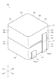
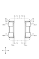
- FIG. 1 is a perspective view showing an example of an inductor assembly according to a first embodiment of the present invention
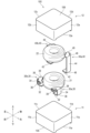
- FIG. 2 is an exploded perspective view of the inductor assembly according to the first embodiment.
- FIG. 2 is an exploded view of the inductor assembly according to the first embodiment, showing a perspective view from below.
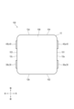
- FIG. 2 is a top view of the inductor assembly according to the first embodiment.
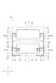
- FIG. 2 is a front view of the inductor assembly according to the first embodiment.
- FIG. 2 is a right side view of the inductor assembly according to the first embodiment.
- FIG. 2 is a bottom view of the inductor assembly according to the first embodiment.
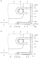
- Fig. 8(a) is an enlarged view of an example of the second terminal in Fig. 5.
- Fig. 8(b) is an enlarged view of another example of the second terminal in Fig. 5.
- the various components of the inductor assembly of the present invention do not need to be independent entities, and it is permitted that multiple components are formed as a single member, that one component is formed from multiple members, that one component is part of another component, or that part of one component overlaps with part of another component, etc.
- the manufacturing method of the inductor assembly of the present invention may be described using a number of steps described in a sequential order, but the order of the steps does not limit the order or timing of performing the steps. Therefore, when implementing the manufacturing method, the order of the steps may be changed to the extent that does not interfere with the content, and some or all of the timing of performing the steps may overlap with each other.
- the front-rear, left-right, top-bottom directions are defined as shown in the drawings. However, this is defined for convenience in order to easily explain the relative relationships between components, and does not limit the directions during manufacture or use of the product embodying the present invention.
- the top-bottom direction is the vertical direction with respect to the mounting board when the inductor assembly is mounted on the mounting board.
- the lower side (lower side) in the top-bottom direction refers to the mounting board side of the inductor assembly when the inductor assembly is mounted on the mounting board.
- the upper side is the opposite side of the lower side in the top-bottom direction.
- the top-bottom direction may or may not coincide with the vertical direction.
- the front-rear direction and the left-right direction may be collectively referred to as the lateral direction.
- the lateral direction may be the horizontal direction, but it does not have to be the horizontal direction.
- the term "flat surface” as used herein means a shape that is physically formed with a flat surface as a goal, and it is not necessarily required that the surface be a geometrically perfect flat surface.
- FIG. 1 is a perspective view showing an example of an inductor assembly 100 according to a first embodiment of the present invention.
- the inductor assembly 100 has a first core (first core 11) and a second core (second core 12).
- the first core contains a first coil (first coil 21).
- the second core contains a second coil (second coil 22).
- the second core is a core different from the first core.
- the second core is disposed on the first core.
- the inductor assembly 100 has a plurality of side surfaces 101 to 104.
- the plurality of side surfaces 101 to 104 in the inductor assembly include side surfaces 11a to 11d of the first core 11 and side surfaces 12a to 12d of the second core 12, respectively.
- the pair of first terminals 30 (30a, 30b) are electrically connected to the first coil 21.
- Each of the pair of first terminals 30 protrudes from a side surface (side surface 11a or side surface 11c) of the first core 11.
- Each of the pair of first terminals 30 has a mounting portion 32 and a standing portion 34.
- the mounting portion 32 is disposed along the lower surface 105 of the inductor assembly 100.
- the standing portion 34 stands upright relative to the mounting portion 32.
- the pair of second terminals 40 (40a, 40b) are electrically connected to the second coil 22.
- Each of the pair of second terminals 40 protrudes from a side surface (side surface 12a or side surface 12c) of the second core 12.
- Each of the pair of second terminals 40 has a mounting portion 42 and a standing portion 44.
- the mounting portion 42 is aligned along the lower surface 105 of the inductor assembly 100, and the standing portion 44 stands relative to the mounting portion 42.
- the rising portion 34 of one first terminal 30a and the rising portion 44 of one second terminal 40a are formed on a first side surface 101 of the inductor assembly 100.
- the pair of first terminals 30a, 30b and the pair of second terminals 40a, 40b are not formed on a second side surface 102 different from the first side surface 101 of the inductor.
- Patent Document 2 discloses an inductor assembly in which two cores (stainless alloy powder blocks (3)) are arranged side by side. The base (5) covers the upper surfaces of the two cores.
- the base (5) is useful for adsorbing the inductor assembly to a mounter when mounting the inductor assembly on a mounting board.
- the base (5) is also useful for integrating the two cores.
- the first core 11 and the second core 12 are arranged in the vertical direction.
- the upper surface 106 of the inductor assembly 100 is the upper surface of the second core 12 and has a predetermined area. Therefore, the upper surface 106 of the inductor assembly of this embodiment can be adsorbed by the mounter.
- the second terminal 40 extending from the upper second core 12 is fitted into the terminal recess 11e below the first core 11. The second core 12 and the first core 11 are combined and integrated by the second terminal 40.
- the inductor assembly 100 is an electronic component including two or more inductors.
- An inductor is an element having at least one coil and at least one core.
- An electronic component is incorporated into a part of an electronic circuit to form a part of an electric device.
- the inductor assembly 100 in this embodiment includes two or more inductors and does not include other elements (transformer, antenna, etc.). Although the inductor assembly 100 in this embodiment includes two inductors, the inductor assembly 100 may include three or more inductors. In addition, it is preferable that two or more inductors are integrated in the inductor assembly 100.
- two or more inductors are integrated means that the inductors are configured to be connected to each other so as not to be separated.
- the first core 11 (first inductor) and the second core 12 (second inductor) are connected by fitting the second terminal 40 into a terminal recess 11e formed on the lower surface 105 of the first core 11 as described later.
- the two inductors may be held by other members.
- the two inductors may be configured not to be separated by a mechanical structure.
- the two inductors may be configured to be bonded with an adhesive or the like so as not to be separated.
- the fact that the two inductors are integrated does not include the fact that the two inductors are bonded to the mounting board and do not separate from each other any further.
- the inductor assembly 100 has a first core 11 and a second core 12.
- the first core 11 is a core in a first inductor
- the second core 12 is a core in a second inductor.
- the core is a magnetic member made of a magnetic material. Examples of the magnetic material include ferrite.
- the core surrounds a coil described later and enters the coil radially inside, so that the core forms a closed loop as a whole. More specifically, the core of this embodiment is integrally formed by placing the coil and terminals (first terminal 30 and second terminal 40) in a mold and pouring a resin containing a magnetic material such as ferrite into the mold.
- the first inductor and the second inductor in the inductor assembly 100 of this embodiment are each a molded coil.
- the core may be configured as a plurality of separate members.
- the core has a flat, approximately rectangular parallelepiped shape.
- the shape of the bottom surface of the core is approximately square.
- the bottom surface of the first core 11 and the bottom surface of the second core 12 have approximately the same shape and dimensions.
- the second core 12 is placed on the first core 11 so that they overlap each other in a plan view.
- the first core 11 and the second core 12, which are approximately rectangular parallelepiped shaped, are arranged in the vertical direction, so that the inductor assembly 100 has an approximately rectangular parallelepiped shape.
- the upper surface of the first core 11 and the second core 12 are bonded by an adhesive (not shown). This prevents the first core 11 and the second core 12 from being misaligned.
- the adhesive may or may not be disposed between a terminal recess 12e (described later) of the second core 12 and the upper surface of the first core 11.
- the first core 11 and the second core 12 may simply be in contact (abutment) without being bonded by an adhesive.
- An engagement portion that engages the first core 11 and the second core 12 with each other may be provided to fix the relative positional relationship between the first core 11 and the second core 12.
- a recess or a protrusion may be provided on the upper surface of the first core 11 or the lower surface of the second core 12, respectively, and the recess and the protrusion may be engaged with each other.
- the inductor assembly 100, the first core 11, and the second core 12 may not be substantially rectangular parallelepiped in shape.
- the inductor assembly 100, the first core 11, and the second core 12 may be prisms whose bottom surfaces are polygonal other than rectangular.
- the bottom surface of each core of this embodiment is formed with a terminal recess 11e, 12e.
- the terminal recess 11e, 12e is a bottomed recess recessed upward from the bottom surface of the core.
- the terminal recess 11e, 12e is open downward and to the side (to the right or left in this embodiment). As shown in FIG. 5 , the ceiling surfaces of the terminal recesses 11 e and 12 e (the bottom surfaces of the terminal recesses 11 e and 12 e which are recessed upward and have a bottom) are inclined upward toward the inside of the inductor assembly 100 . As shown in FIG. 1, the first core 11 and the second core 12 each have a plurality of side surfaces. The first core 11 has a plurality of side surfaces 11a, 11b, 11c, and 11d. The second core 12 has a plurality of side surfaces 12a, 12b, 12c, and 12d.
- One of the side surfaces of the first core 11 is arranged so as to continue to one of the side surfaces of the second core 12.
- “arranged so that the surfaces continue to each other” means that the sides of the ends of the surfaces are arranged close to each other and are arranged on approximately the same plane.
- the surfaces may be partially separated from each other.
- one of the side surfaces 11a to 11d of the first core 11 and one of the side surfaces 12a to 12d of the second core 12 each form one of the side surfaces 101 to 104 of the inductor assembly 100.
- the side surface 11a of the first core 11 and the side surface 12a of the second core 12 form a first side surface 101 of the inductor assembly 100.
- the side surface 11b of the first core 11 and the side surface 12b of the second core 12 form a second side surface 102 of the inductor assembly 100.
- the side surface 11c of the first core 11 and the side surface 12c of the second core 12 form a third side surface 103 of the inductor assembly 100.
- the side surface 11d of the first core 11 and the side surface 12d of the second core 12 form a fourth side surface 104 of the inductor assembly 100.
- the inductor assembly 100 has a first coil 21 and a second coil 22 as coils.
- the first coil 21 is a coil in the first inductor
- the second coil 22 is a coil in the second inductor.
- the coil is formed by winding a coil wire.
- the coil wire is wound with the winding axis in the up-down direction, but this is not limited to this.
- the coil wire may be wound with the winding axis in the left-right direction or the front-back direction.
- the coil wire is made of a conductive material (e.g., a metal such as copper).
- the coil wire may be a round wire with a circular cross section, or a flat wire with a flat cross section (e.g., a quadrilateral or ellipse).
- Both ends of the coil wire are drawn out from the winding part of the coil.
- the ends of the coil wire may be drawn out from the winding part near the center in the thickness direction (vertical direction) of the winding part of the coil, or may be drawn out from the winding part at the upper or lower side in the thickness direction.
- both ends of the coil wire may be drawn out from the winding part at the same height (position in the vertical direction) or may be drawn out from the winding part at different heights. For example, both ends may be drawn out from the winding part near the center in the thickness direction of the winding part.
- one end may be drawn out from the winding part at the upper side in the thickness direction of the winding part, and the other end may be drawn out from the winding part at the lower side in the thickness direction.
- both ends of the coil wire are pulled out from the winding portion at two positions on either side of the winding portion, but the present invention is not limited to this and both ends of the coil wire may be pulled out from any positions.
- the end of the coil wire is electrically connected to a terminal (first terminal 30 or second terminal 40).
- a terminal first terminal 30 or second terminal 40
- the end of the coil wire forming the first coil 21 is electrically connected to the first terminal 30, and the end of the coil wire forming the second coil 22 is electrically connected to the second terminal 40.
- the end of the terminal inserted into the core is bent into a U-shape.
- the end of the terminal holds the end of the coil wire and sandwiches the end of the coil wire in the vertical direction.
- the end of the coil wire and the end of the terminal are joined by a method such as laser welding or resistance welding.
- the mode of electrical connection between the coil wire and the terminal is not limited to direct contact as described above.
- the coil wire and the terminal may be electrically connected via a separate member.
- the end of the coil wire may be wound around a winding terminal that is a separate member from the terminal, and the winding terminal and the terminal may be connected to each other, so that the coil wire and the terminal are electrically connected via the winding terminal.
- the coil wire and the terminal may also be integrally formed from the same member.
- the terminals are input/output terminals, and each inductor is connected to other electronic components or electric devices via the terminals.
- the terminal is made of a conductive material, such as a metal such as copper, and the terminal of this embodiment is formed by bending a plate-shaped conductive material.
- the terminals of this embodiment have embedded portions 39, 49, standing portions 34, 44 and mounting portions 32, .
- the embedded portion 39 is embedded in the first core 11 or the second core 12.
- the embedded portions 39, 49 are parts of the terminal embedded inside the core. In other words, a part of the terminal continuing from the embedded portion 39, 49 protrudes laterally (towards either the left or right direction) from the core.
- the embedded portion 39 is the end of the terminal that is conductive with the coil wire, and is also the base end. One end of the terminal that is conductive with the coil wire is called the base end, and the other end opposite to the one end is called the tip.
- the entire terminal may be disposed outside the core, and the terminal may not have the embedded portion 39, 49.
- the mounting portions 32 and 42 are parts of the terminals including a mounting surface that is grounded to the mounting board.
- the inductor assembly 100 is mounted by joining the mounting portions 32 and 42 to the mounting board by soldering or the like.
- the mounting portions 32 and 42 and the mounting surface are aligned with the lower surface 105 (the lower surface of the first core 11) of the inductor assembly.
- the mounting portions 32 and 42 and the mounting surface are aligned with the lower surface 105 of the inductor assembly 100 means that the mounting portions 32 and 42 and the mounting surface are substantially parallel to the lower surface 105 of the inductor assembly 100.
- the terminals are bent inward at the first bent portions 36 and 46, and the mounting portions 32 and 42 and the mounting surface are aligned close to the lower surface 105 of the inductor assembly 100.
- the mounting portions 32 and 42 are aligned with the ceiling surface of the terminal recess 11e. That is, the mounting portions 32 and 42 are substantially parallel to the ceiling surface of the terminal recess 11e.
- the inclination angle of the ceiling surface of the terminal recess 11e is different from the inclination angle of the mounting portions 32, 42 and are not completely parallel.
- the terminals may be bent outward at the first bent portions 36, 46, and the mounting portion 32 and the mounting surface may be disposed to the side of the inductor assembly 100 and along the lower surface 105 of the inductor assembly 100. 5 and 7, the mounting portions 32, 42 are disposed in the terminal recess 11e of the first core 11. In this embodiment, the mounting portions 32 of the first terminals 30 and the mounting portions 42 of the second terminals 40 that are arranged laterally are both disposed in one terminal recess 11e.
- one or more terminal recesses 11e may be formed in the bottom surface of the core in a number corresponding to the number of terminals, and one or more mounting portions 32, 42 of the terminals may be disposed in each terminal recess 11e.
- the rising portions 34, 44 are parts of the terminals that rise relative to the mounting portions 32, 42.
- the rising portions 34, 44 are located between the embedded portion (base end) and the mounting portion (tip end).
- the rising portions 34, 44 rising relative to the mounting portions 32, 42 means that the rising portions 34, 44 extend so as to cross the mounting portions 32, 42.
- the extending direction of the rising portions 34, 44 includes more directional components perpendicular to the extending direction of the mounting portions 32, 42 than the extending direction components of the mounting portions 32, 42. Even more preferably, the extending direction of the rising portions 34, 44 is approximately in the vertical direction.
- the rising portions 34, 44 are disposed along the side surfaces 101 to 104 of the inductor assembly 100.
- the rising portions 34, 44 may be in contact (abutment or pressure contact) with the side surfaces 101 to 104 of the inductor assembly 100, or may be spaced apart.
- the standing portions 34, 44 of each terminal are disposed laterally outward from the center of the inductor assembly 100 in the lateral direction (front-back direction) when viewed facing the plate surface (main surface) of the standing portions 34, 44 (when viewed in the left-right direction). This fixes the relative positional relationship between the first core 11 and the second core 12.
- the first core 11 is prevented from being misaligned with respect to the second core 12 so as to rotate about the vertical direction as a rotation axis.
- the upright portions 34, 44 have a substantially linear shape extending in the vertical direction. As shown in FIG.
- the upper part of the standing part 44 of the second terminal 40 may be curved toward the core (first core 11 and second core 12) (so as to approach the side surfaces 11a, 11c of the first core 11 and the side surfaces 12a, 12c of the second core 12 shown in FIG. 1). That is, the upper part of the standing part 44 of the second terminal 40 may be recessed toward the inside. This allows the second terminal 40 to hold the first core 11 and the second core 12 well.
- a part of the standing part 44 is in close contact with the side surface of the core (the side surfaces 11a, 11c of the first core 11 or the side surfaces 12a, 12c of the second core 12) without any gap.
- the entire standing part 44 may be separated from the side surface of the core.
- the upper part of the standing portion 44 of the second terminal 40 is a part of the second terminal 40 that is arranged above the first terminal 30 (particularly the second bent portion 38 of the first terminal 30).
- the upper part of the standing portion 44 of the second terminal 40 is a part of the second terminal 40 that is along the lower part of the side surfaces 12a, 12c (see FIG. 1) of the second core 12 and the upper part of the side surfaces 11a, 11c (see FIG. 1) of the first core 11.
- the lower part of the second terminal 40 (a part along the lower part of the side surfaces 11a, 11c of the first core 11) and the first terminal 30 may have a substantially linear shape or a curved shape closer to a linear shape. That is, the upper part of the standing portion 44 of the second terminal 40 may be curved more than the lower parts of the first terminal 30 and the second terminal 40.
- the curved shape of the second terminal 40 is exaggerated in FIG. 5 for convenience.
- the inductor assembly 100 may have a shape closer to a straight line than the curved shape shown.
- the second terminal 40 is bent at a substantially right angle at the second bent portion 48.
- the second terminal 40 may be bent at the second bent portion 48 so as to bulge slightly outward.
- the first terminal 30 and the second terminal 40 may have a generally linear shape as a whole.
- the terminals are bent at first bent portions 36, 46 so that the mounting portions 32, 42 are disposed below the inductor assembly 100.
- the first bent portions 36, 46 are located between the standing portions 34, 44 and the mounting portions 32, 42. That is, in this embodiment, the terminals are bent inward from the standing portions 34, 44 to the mounting portions 32, 42.
- the inward direction refers to the direction toward the inside of the inductor assembly 100.
- the first bent portions 36, 46 are bent in a curved shape. Instead of this embodiment, the first bent portions 36, 46 may be bent in an angular shape.
- the first bent portions 36, 46 are bent in a shape that follows the corner formed by the side surfaces 101, 103 and the lower surface 105 of the inductor assembly 100.
- the term "terminal is bent” includes not only a terminal that is bent to form a corner, but also a terminal that is curved in an arc and does not have a clear corner.
- the first bent portion 36, 46 is a part of the terminal having a larger curvature than the standing portion 34, 44 or the mounting portion 32, 42. Since the standing portion 34, 44 and the mounting portion 32, 42 are substantially linear, the portion of the terminal having a curved shape between the standing portion 34, 44 and the mounting portion 32, 42 is the first bent portion 36, 46.
- Each of the terminals is bent at the second bent portion 38, 48.
- the second bent portion 38, 48 is located between the embedded portion 39, 49 and the standing portion 34, 44. That is, in this embodiment, the terminal is bent downward from the embedded portion 39, 49 to the standing portion 34, 44.
- the second bent portion 38, 48 is bent in a curved shape.
- the second bent portion 38, 48 may be bent in an angular shape.
- the terminal is bent immediately after protruding from the core (first core 11 or second core 12) to form the second bent portion 38, 48.
- the second bent portions 38, 48 are parts of the terminal having a greater curvature than the standing portions 34, 44 or the embedded portions 39, 49. Since the standing portions 34, 44 are substantially linear, the second bent portions 38, 48 are the parts of the terminal that protrude from the core and have a curved shape between the standing portions 34, 44 and the base end of the terminal that is outside the core.
- the standing portion 34 of one first terminal 30a and the standing portion 44 of one second terminal 40a are formed on the first side surface 101 (on the same side surface).
- the standing portions 34, 44 being formed on the first side surface 101 means that the standing portions 34, 44 are arranged extending on the surface of the first side surface 101.
- the standing portions 34, 44 may be arranged on the first side surface 101 in contact (abutting or pressing) with the first side surface 101, or may be arranged on the first side surface 101 apart from the first side surface 101.
- the standing portions 34, 44 are formed on the surface of the inductor assembly 100 facing laterally.
- the side surfaces 101 to 104 along which the standing portions 34, 44 of the inductor assembly 100 are located are flat surfaces.
- a groove extending in the vertical direction may be formed in the side surfaces 101-104 of the inductor assembly 100, and at least a part of the standing portions 34, 44 may be embedded in the groove. That is, the standing portions 34, 44 may be formed on the bottom surface of the groove.
- the bottom surface of the groove is also part of the side surfaces 101-104 of the inductor assembly 100. 6, the rising portion 34 of the first terminal 30a and the rising portion 44 of the second terminal 40a are arranged along each other.
- the first terminal 30a and the second terminal 40a extend in substantially the same direction (up-down direction). Moreover, the first terminal 30a and the second terminal 40a are arranged side-by-side in the front-rear direction.
- the pair of first terminals 30a, 30b and the pair of second terminals 40a, 40b are not formed on a second side surface 102, which is one of the sides 101 to 104 of the inductor assembly 100 different from the first side surface 101. That is, the pair of first terminals 30a, 30b and the pair of second terminals 40a, 40b are not disposed on the second side surface 102.
- the second side 102 when viewed facing the second side surface 102, the entire second side surface 102 is exposed from the pair of first terminals 30a, 30b and the pair of second terminals 40a, 40b.
- the second side 102 is a side adjacent to the side 101, but is not limited thereto.
- the second side 102 may be a side not adjacent to the side 101.
- the second side surface 102 is a side surface facing the side surface 101 or a side surface adjacent to the side surface 101.
- the second side surface 102 is a side surface facing the first side surface 101 at 180 degrees, a side surface facing the first side surface 101 at 120 degrees, or a side surface adjacent to the first side surface 101.
- the second side surface 102 is a side surface facing the first side surface 101 at 180 degrees or a side surface facing the first side surface 101 at 90 degrees. This allows the inductor assembly 100 to be disposed in close proximity to other components disposed in the front, back, left, right, and right directions.
- the third side surface 103 is one of the side surfaces of the inductor assembly 100.
- the third side surface 103 faces the first side surface 101.
- the pair of first terminals 30a, 30b and the pair of second terminals 40a, 40b are not formed on the fourth side surface 104.
- the fourth side surface 104 is one of the side surfaces of the inductor assembly 100.
- the fourth side surface 104 faces the second side surface 102. This makes it possible to place other components closely on the opposing fourth side surface 104 in addition to the second side surface 102, thereby enabling the mounting board to be used in a more space-saving manner.
- first side surface 101 and the third side surface 103 are opposed to each other at an angle of 180 degrees, and the second side surface 102 and the fourth side surface 104 are also opposed to each other at an angle of 180 degrees.
- first side surface 101 and the third side surface 103 may be opposed to each other at an angle of 90 degrees, and the second side surface 102 and the fourth side surface 104 may also be opposed to each other at an angle of 90 degrees. That is, in the inductor assembly 100 having a quadrilateral bottom surface and four side surfaces, the first side surface 101 and the third side surface 103 may be adjacent side surfaces, and the second side surface 102 and the fourth side surface 104 may also be adjacent side surfaces.
- the standing portion 34 of the other first terminal 30b and the standing portion 44 of the other second terminal 40b may be formed on the first side surface 101, and the pair of first terminals 30a, 30b and the pair of second terminals 40a, 40b may not be formed on the third side surface 103 and the fourth side surface 104.
- all of the two standing portions 34, 34 of the pair of first terminals 30a, 30b and the two standing portions 44, 44 of the pair of second terminals 40a, 40b may be formed on the first side surface 101.
- the first terminals 30a, 30b and the second terminals 40a, 40b are arranged side by side in a predetermined arrangement direction (front-rear direction) on each of the first side surface 101 and the third side surface 103.
- the first terminal 30a and the other first terminal 30b are arranged on the same side (front side) in the arrangement direction (front-rear direction) with respect to the second terminal 40a or the other second terminal 40b.
- the first terminal 30a is arranged on the front side in the front-rear direction with respect to the second terminal 40a
- the other first terminal 30b is also arranged on the front side in the front-rear direction with respect to the other second terminal 40b.
- the first terminal 30 and the second terminal 40 may have different shapes, for example, as described later, and the heights of the mounting parts 32, 42 may differ slightly between the first terminal 30 and the second terminal 40. That is, the difference in height between the mounting parts 32, 32 of the pair of first terminals 30a, 30b and the mounting parts 42, 42 of the pair of second terminals 40a, 40b may be greater than the difference in height between the mounting parts 32, 32 of the pair of first terminals 30a, 30b, or the difference in height between the mounting parts 42, 42 of the pair of second terminals 40a, 40b.
- the grounding of each terminal to the mounting board is improved compared to the case where the first terminal 30a is arranged in front of the second terminal 40a and the first terminal 30b is arranged behind the second terminal 40b. Even if there is a large difference in height between the mounting portion 32 of the first terminals 30a, 30b and the mounting portion 42 of the second terminals 40a, 40b, the inductor assembly 100 can be tilted slightly forward or backward to allow the four terminals to be well grounded to the mounting board.
- the predetermined arrangement direction in which the first terminal 30 and the second terminal 40 are arranged laterally is the horizontal direction, and in particular, the direction along the first side surface 101 or the third side surface 103 (the side surface along which the first terminal 30 and the second terminal 40 are arranged).
- the predetermined arrangement direction of the first terminal 30 and the second terminal 40 arranged laterally with the first terminal 30 may be simply referred to as the arrangement direction.
- first terminal 30a and the other first terminal 30b are each arranged on the same side as one second terminal 40a or the other second terminal 40b, this means that when viewed from a specified direction (for example, when viewed in a plan view), the pair of first terminals 30a, 30b are arranged on the same side (front side) of the pair of second terminals 40a, 40b.
- the pair of first terminals 30a, 30b or the pair of second terminals 40a, 40b face each other. More specifically, the first terminals 30a, 30b or the second terminals 40a, 40b at least partially (in the present embodiment, substantially entirely) overlap each other when viewed from the side (viewed from the left-right direction).
- the central distance L1 is equal to or greater than the edge distance L2 (the sum of the first edge distance L2a and the second edge distance L2b).
- the edge distance L2 is the sum of the first edge distance L2a and the second edge distance L2b.
- the insulation distance between the second terminal 40 of the front inductor assembly 100 and the first terminal 30 of the rear inductor assembly 100 is maintained, while the insulation distance between the first terminal 30 and the second terminal 40 in each inductor assembly 100 (insulation distance within inductor assembly) is also maintained.
- the distance between the inductor assemblies includes the edge distance L2 and the width of the gap between the inductor assemblies 100, which will be described later. Therefore, by making the center distance L1 equal to or greater than L2, the distance between the inductor assemblies and the distance within the inductor assembly can be made substantially the same.
- the center distance L1 is the distance between the first terminals 30a, 30b and the second terminals 40a, 40b arranged side by side in the arrangement direction on the first side surface 101 or the third side surface 103. Specifically, the center distance L1 is the shortest distance in the lateral direction (front-rear direction) between the side end face of the first terminal 30a and the side end face of the second terminal 40a on the first side surface 101, or between the side end face of the first terminal 30b and the side end face of the second terminal 40b on the third side surface 103.
- the first edge distance L2a is the distance between the first end 107a of the first side surface 101 or the third side surface 103 and the first terminals 30a, 30b.
- the first end 107a is the end 107 of the first side surface 101 or the third side surface 103 in the arrangement direction, and is the end 107 of the first side surface 101 or the third side surface 103 close to the first terminals 30a, 30b.
- the end 107 is an edge in the front-rear direction of the first side surface 101 or the third side surface 103.
- the end 107 of the first side surface 101 is the side that is the boundary between the first side surface 101 and the second side surface 102, and the side that is the boundary between the first side surface 101 and the fourth side surface 104.
- the end 107 in the third side surface 103 is the side which is the boundary between the third side surface 103 and the second side surface 102, and the side which is the boundary between the third side surface 103 and the fourth side surface 104.
- the first end 107a in the first side surface 101 is the side which is the boundary between the first side surface 101 and the second side surface 102
- the first end 107a in the third side surface 103 is the side which is the boundary between the third side surface 103 and the second side surface 102.
- the distance between the first end 107a and the first terminals 30a, 30b is the shortest distance in the lateral direction (front-rear direction) between the first end 107a and the side end surfaces of the first terminals 30a, 30b.
- the second edge distance L2b is the distance between the second end 107b of the first side surface 101 or the third side surface 103 and the second terminals 40a, 40b.
- the second end 107b is the end 107 of the first side surface 101 or the third side surface 103 in the arrangement direction, and is the end 107 of the first side surface 101 or the third side surface 103 that is close to the second terminal.
- the second end 107b of the first side surface 101 is the side that is the boundary between the first side surface 101 and the fourth side surface 104
- the second end 107b of the third side surface 103 is the side that is the boundary between the third side surface 103 and the fourth side surface 104.
- the distance between the second end 107b and the second terminals 40a, 40b is the shortest distance along the lateral direction (front-rear direction) between the first end 107a and the side end surface of the second terminals 40a, 40b.
- the difference between the center distance L1 and the edge distance L2 is preferably smaller than the width dimension (the dimension in the lateral direction, particularly the front-rear direction) of the first terminal 30 or the second terminal 40. This ensures that the edge distance L2 is sufficient to ensure the insulation distance between adjacent inductor assemblies 100.
- the first edge distance L2a and the second edge distance L2b are equal to each other.
- the first edge distance L2a and the second edge distance L2b being equal to each other means that the first edge distance L2a is half or more of the second edge distance L2b and is equal to or less than twice the second edge distance L2b.
- the center distance L1 and the edge distance L2 may be equal to each other.
- center distance L1 and the edge distance L2 being equal to each other means that the center distance L1 is equal to or more than half the edge distance L2 and equal to or less than twice the edge distance L2.
- the center distance L1 may be smaller than the edge distance L2.
- the tip 42a of the mounting portion 42 of the second terminals 40a, 40b is disposed further inward of the inductor assembly 100 than the tip 32a of the mounting portion 32 of the first terminals 30a, 30b arranged side by side with the second terminals 40a, 40b.
- the first terminal 30 and the second terminal 40 are illustrated in Fig. 7 to further emphasize this configuration. That is, a tip distance L3, which will be described later, is illustrated larger than it actually is.
- the second terminal 40 extends from the second core 12 and is bent so as to embrace the first core 11, and holds the first core 11 together with the second core 12.
- the tip 42a of the second terminal 40 is disposed closer to the inside of the inductor assembly 100 than the tip 32a of the first terminal 30, so that the second terminal 40 can hold the first core 11 more satisfactorily.
- the second terminal 40 extends to a position higher than the first terminal 30, the load on the joint surface between the mounting portion 42 of the second terminal 40 and the mounting substrate is likely to be greater than the load on the joint surface between the mounting portion 32 of the first terminal 30 and the mounting substrate. If the tip 42a of the second terminal 40 is positioned further inward in a plan view, the ground surface between the second terminal 40 and the mounting substrate becomes larger. As a result, the second terminal 40 is more firmly joined to the mounting substrate, and the durability of the joint surface between the second terminal 40 and the mounting substrate against loads is improved.
- the tip 32a, 42a of the mounting portion 32, 42 is an end of the mounting portion 32, 42 opposite the side continuing to the upright portion 34, 44.
- the tip 32a, 42a of the mounting portion 32, 42 is an end on the inside of the inductor assembly 100 in the mounting portion 32, 42 when viewed in a plan view.
- the inside of the inductor assembly 100 when viewed from a specific direction is the direction from the outer edge of the inductor assembly 100 toward the center of the inductor assembly 100 when the inductor assembly 100 is viewed from the specific direction.
- the tip 42a of one second terminal 40a is disposed to the left of the tip 32a of one first terminal 30a.
- the tip 42a of the other second terminal 40b is disposed to the right of the tip 32a of the other first terminal 30b.
- the area of the mounting portion 42 of one second terminal 40a is larger than the area of the mounting portion 32 of one first terminal 30a.
- the area of the mounting portion 42 of the other second terminal 40b is larger than the area of the mounting portion 32 of the other first terminal 30b.
- the area of the mounting portions 32, 42 may be the area of the mounting portions 32, 42 when facing the mounting portions 32, 42, or may be the area of the mounting portions 32, 42 when viewed from below.
- the tip 42a of the second terminal 40 is preferably disposed inside the inductor assembly 100 from the tip 32a of the first terminal 30 by a length equal to or greater than the thickness dimension of the first terminal 30 or the second terminal 40. That is, the distance (tip distance L3) between the tip 42a of the second terminal 40 and the tip 32a of the first terminal 30 in the extension direction (left-right direction) of the mounting parts 32, 42 is preferably equal to or greater than the thickness dimension of the first terminal 30 or the second terminal 40 (particularly the mounting parts 32, 42). This allows the area of the mounting part 42 of the second terminal 40 to be sufficiently large.
- the tip 32a of the first terminal 30 may be disposed further inside the inductor assembly 100. That is, the tip 42a of the second terminal 40 may be disposed inside the inductor assembly 100 from the tip 32a of the first terminal 30 by a length equal to or less than the thickness dimension of the first terminal 30 or the second terminal 40. That is, the tip distance L3 may be the same as or smaller than the thickness dimension of the first terminal 30 or the second terminal 40 .
- the second terminal 40 is bent at two points (bending points 46a, 46b) in the first bent portion 46.
- the crack is likely to stop at the bending points 46a, 46b and their vicinity.
- the bonding between the second terminal 40 and the solder is improved. Note that, for convenience, in Fig. 8(a) and Fig. 8(b), the bending shape at the first bending portion 46 of the second terminal 40 is exaggerated compared to the actual shape. In reality, the bending shape at the first bending portion 46 of the second terminal 40 may be closer to the bending shape at the first bending portion 36 of the first terminal 30.
- the bending points 46a and 46b are the centers of particularly steeply bent portions in the first bent portion 46. That is, there are two portions (portions that bend more steeply than other portions) that have a smaller radius of curvature than other portions (portions in the vicinity of the bending points 46a and 46b, such as the intermediate portion 46c) in the first bent portion 46 of the second terminal 40.
- the bending centers of the two portions or portions including the vicinity of the centers are the bending points 46a and 46b.
- the two bending points 46a, 46b are spaced apart from each other.
- An intermediate portion 46c sandwiched between the spaced apart bending points 46a, 46b is either linear or has a larger curved shape than the bending points 46a, 46b and their vicinity.
- the radius of curvature of the second terminal 40 at the bending point 46b on the tip side is smaller than the radius of curvature of the second terminal 40 at the bending point 46a on the base side. That is, the second terminal 40 is bent more steeply at the bending point 46b on the tip side than at the bending point 46a on the base side.
- This allows a larger mounting surface, which is a flat surface, in the mounting portion 42 to be secured. As a result, the bonding between the mounting portion 42 and the mounting board is improved.
- the radius of curvature of the second terminal 40 at the bending point 46b on the tip side may be larger than the radius of curvature of the second terminal 40 at the bending point 46a on the base side.
- the second terminal 40 may be bent into a curved shape larger at the bending point 46b on the tip side than at the bending point 46a on the base side. This allows the stress on the second terminal 40 applied at the bending point 46a on the tip side to be well alleviated.
- the bending angle of the second terminal 40 at the bending point 46b on the tip side is larger than the bending angle of the second terminal 40 at the bending point 46a on the base side. That is, the minimum angle between the approximate extension direction of the intermediate portion 46c and the extension direction of the mounting portion 42 is smaller than the minimum angle between the approximate extension direction of the intermediate portion 46c and the standing portion 34. With this configuration, the intermediate portion 46c is inclined at an angle of less than 45 degrees with respect to the horizontal.
- the intermediate portion 46c is disposed closer to the mounting substrate, so that the bonding between the intermediate portion 46c and the mounting substrate is improved, and the inductor assembly 100 is more properly fixed to the mounting substrate.
- the first terminal 30 is bent at one location at the first bent portion 36.
- the first terminal 30 may be bent at two or more locations at the first bent portion 36.
- the first bent portion 46 of the second terminal 40 is closer to the first core 11 than the first bent portion 36 of the first terminal 30. More specifically, when viewed in the arrangement direction (front-rear direction) of the first terminal 30 and the second terminal 40, the middle portion 46c is closer to the first core 11 than the bending center of the first bent portion 36 of the first terminal 30. As a result, the second terminal 40 is bent at the first bent portion 46 so as to be closer to the first core 11. As a result, the second terminal 40 can hold the first core 11 better.
- the second terminal 40 does not have two or more bending points 46a, 46b and is curved more than the first terminal 30, the bending center of the first bent portion 46 of the second terminal 40 is closer to the first core 11 than the bending center of the first terminal 30.
- the radius of curvature of the first bent portion 46 of the second terminal 40 may be larger than the radius of curvature of the first bent portion 36 of the first terminal 30 arranged side by side with the second terminal 40.
- the bent shape of the first terminal 30 or the second terminal 40 as described above may be formed by applying different magnitudes of force to each terminal or by applying stress to different parts of each terminal. Since the second terminal 40 is not bent as sharply as the first terminal 30, the stress applied to the second terminal 40 can be more effectively alleviated. Therefore, the second terminal 40 is more firmly fixed to the mounting substrate.
- a larger space is created between the mounting substrate and the first bent portion 46 of the second terminal 40, which has a larger radius of curvature, compared to the space between the first terminal 30 and the mounting substrate. Therefore, more solder can be accumulated between the second terminal 40 and the mounting substrate, and the second terminal 40 and the mounting substrate can be more firmly joined. This allows the second terminal 40, which is more susceptible to load than the first terminal 30, to be more firmly fixed to the mounting substrate.
- the second terminal 40 may be bent at the first bent portion 46 into a circular arc shape, or may be bent into a curved shape with a non-constant radius of curvature, such as an elliptical arc shape.
- the radius of curvature of the first bent portion 46 of the second terminal 40 being larger than the radius of curvature of the first bent portion 36 of the first terminal 30 means, for example, that the maximum value of the radius of curvature of the first bent portion 46 of the second terminal 40 is larger than the radius of curvature of the first bent portion 36 of the first terminal 30.
- the radius of curvature at the tip or base end of the first bent portion 46 of the second terminal 40 may be larger than the radius of curvature at the tip or base end of the first bent portion 36 of the first terminal 30.
- the distance between the base end and the tip of the first bent portion 46 of the second terminal 40 (the distance between the base end and the tip on a straight line connecting the base end and the tip) may be larger than the distance between the base end and the tip of the first bent portion 36 of the first terminal 30.
- the radius of curvature at the tip end of the first bent portion 46 of the second terminal 40 is larger than the radius of curvature at the base end of the first bent portion 46. This allows the first bent portion 46 of the second terminal 40 to be disposed so as to be closer to the mounting board, thereby improving the bonding between the first bent portion 46 and the mounting board.
- the angle formed between the standing portion 44 and the mounting portion 42 at the first bent portion 46 of the second terminal 40 is smaller than the angle formed between the standing portion 34 and the mounting portion 32 at the first bent portion 36 of the first terminal 30 arranged laterally next to the second terminal 40.
- the mounting portion 42 of the second terminal 40 may be inclined at a larger inclination angle relative to the lateral direction (or relative to the lower surface 105 of the inductor assembly 100) than the mounting portion 32 of the first terminal 30.
- the inclination angle of the mounting portions 32, 42 relative to the lateral direction refers to the minimum angle formed between the lateral direction and the mounting portions 32, 42.
- the angle formed between the standing portion 44 and the mounting portion 42 at the first bent portion 46 of the second terminal 40 may be greater than the angle formed between the standing portion 34 and the mounting portion 32 at the first bent portion 36 of the first terminal 30 arranged horizontally to the second terminal 40.
- the tip 42a of the second terminal 40 is disposed above the tip 32a of the first terminal 30. More specifically, the tip 42a of the second terminal 40 is closer to the first core 11 (particularly the ceiling surface of the terminal recess 11e) than the tip 32a of the first terminal 30. That is, the inclination angle of the mounting portion 42 of the second terminal 40 with respect to the horizontal direction is larger than the inclination angle of the ceiling surface of the terminal recess 11e with respect to the horizontal direction. Also, as described above, the inclination angle of the mounting portion 42 of the second terminal 40 with respect to the horizontal direction is larger than the inclination angle of the mounting portion 32 of the first terminal 30 with respect to the horizontal direction.
- the inductor assembly 100 has the above-mentioned configuration in a natural state before the inductor assembly 100 is mounted on a mounting board. It is not necessary for the first terminal 30 and the second terminal 40 to have the above-mentioned configuration when the inductor assembly 100 is mounted on a mounting board.
- at least the tips 32a, 42a (or tips including the vicinity of the tips 32a, 42a) of the first terminal 30 and the second terminal 40 are disposed inside the terminal recess 11e. In other words, the tips 32a, 42a or tips of the first terminal 30 and the second terminal 40 are disposed above the lower surface 105 (lowest surface) of the first core 11.
- the tip 32a or tip of the first terminal 30, or the tip 42a or tip of the second terminal 40 may protrude downward from the lower surface 105 (lowest surface) of the inductor assembly 100.
- the lowest point of the first bent portion 46 of the second terminal 40 is disposed lower than the lowest point of the first bent portion 36 of the first terminal 30.
- the first bent portion 46 of the second terminal 40 is disposed so as to be closer to the mounting board than the first bent portion 36 of the first terminal 30. Note that it is sufficient for the inductor assembly 100 to have the above-mentioned configuration in a natural state before the inductor assembly 100 is mounted on a mounting board.
- first terminal 30 and the second terminal 40 it is not necessary for the first terminal 30 and the second terminal 40 to have the above-mentioned configuration when the inductor assembly 100 is mounted on a mounting board.
- at least a part of the first bent portion 36 of the first terminal 30 and at least a part of the first bent portion 46 of the second terminal 40 are disposed to protrude downward from the lower surface 105 (lowest surface) of the inductor assembly 100.
- the lowermost portion of the first bent portion 36 of the first terminal 30 or the lowermost portion of the first bent portion 46 of the second terminal 40 may be at the same height as the lower surface 105 (lowest surface) of the inductor assembly 100.
- the tip 42a of the mounting portion 42 of the second terminal 40 is in contact with the lower surface 105 of the inductor assembly 100.
- the tip 32a of the mounting portion 32 of the first terminal 30 is spaced from the lower surface 105 of the inductor assembly 100.
- the tip 42a of the second terminal 40 comes into contact with the lower surface of the inductor assembly 100 (the bottom surface of the first core 11), thereby allowing the second terminal 40 to better hold the first core 11 and the second core 12.
- the tip 32a of the first terminal 30 is spaced from the lower surface 105 of the inductor assembly 100, so that the mounting portion 32 of the first terminal 30 has springiness without interfering with the inductor assembly 100. This allows the mounting portion 32 of the first terminal 30 to deform in accordance with the mounting substrate when the inductor assembly 100 is mounted on the mounting substrate, thereby allowing the inductor assembly 100 to be mounted on the mounting substrate well.
- the tip 42a of the second terminal 40 may be pressed against the lower surface 105 of the inductor assembly 100 (the tip 42a may bias the lower surface 105 upward), or may simply abut against the lower surface 105 of the inductor assembly 100.
- the tip 42a of the second terminal 40 may also be fitted inside the first core 11. That is, the tip 42a of the second terminal 40 and its vicinity (the tip portion including the tip 42a) may be disposed within the envelope volume of the first core 11. By having the tip portion of the mounting portion 42 bite into the first core 11, the second terminal 40 can better hold the first core 11.
- the radius of curvature of the second bent portion 48 of the second terminal 40 is smaller than the radius of curvature of the second bent portion 38 of the first terminal 30 that is arranged next to the second terminal 40.
- the second terminal 40 is bent sharply at a right angle in the second bent portion 48 while being substantially in contact with the side surfaces 12a, 12c of the second core 12 (bent so as to be close to and along the side surfaces 12a, 12c of the second core 12).
- the second bent portion 38 of the first terminal 30 protrudes slightly outward from the side surfaces 11a, 11c of the first core 11 and then curves gently toward the side surfaces 11a, 11c.
- the gap between the second bent portion 48 of the second terminal 40 and the side surfaces 12a, 12c of the second core 12 is smaller than the gap between the second bent portion 38 of the first terminal 30 and the side surfaces 11a, 11c of the first core 11.
- the difference between the radius of curvature at the second bent portion 48 of the second terminal 40 and the radius of curvature at the second bent portion 38 of the first terminal 30 is exaggerated for convenience. In reality, the difference may be smaller than the difference shown.
- the second bent portion 38 of the first terminal 30 protrudes further outward from the inductor assembly 100 than the second terminal 40 (particularly the second bent portion 48 thereof), but this is not limited thereto.
- the second bent portion 38 of the first terminal 30 may be located at the same position as the second bent portion 48 of the second terminal 40 in the left-right direction. For example, when bending the first terminal 30 or the second terminal 40 at the second bent portion 38, 48, different magnitudes of force may be applied or stress may be applied to different parts of the terminal to form the bent shape of the first terminal 30 or the second terminal 40 as described above.
- the second bent portion 38 of the first terminal 30 may be bent at a right angle or at an angle exceeding a right angle, while the second bent portion 48 of the second terminal 40 may be bent at an acute angle (so that the standing portion 44 tapers downward).
- the bending angle of the second bent portion 48 is slightly widened to a right angle, and the standing portion 44 can be brought into intimate contact with the side surface of the core.
- the second terminal 40 is better aligned with the second core 12 (especially the part near the second bent portion 48). This enables the second terminal 40 to hold the first core 11 and the second core 12 in a better manner.
- the first terminal 30 and the second terminal 40 may be bent at the second bent portions 38, 48 into a circular arc shape, or may be bent into a curved shape with a non-constant radius of curvature, such as an elliptical arc shape.
- the radius of curvature of the second bent portion 38 of the first terminal 30 is larger than the radius of curvature of the second bent portion 48 of the second terminal 40, for example, means that the maximum value of the radius of curvature of the second bent portion 38 of the first terminal 30 is larger than the radius of curvature of the second bent portion 48 of the second terminal 40.
- the radius of curvature at the tip or base end of the second bent portion 38 of the first terminal 30 may be larger than the radius of curvature at the tip or base end of the second bent portion 48 of the second terminal 40.
- the distance between the base end and the tip of the second bent portion 38 of the first terminal 30 (the distance between the base end and the tip on a straight line connecting the base end and the tip) may be larger than the distance between the base end and the tip of the second bent portion 48 of the second terminal 40.
- the present invention is not limited to the above-described embodiment, but includes various modifications and improvements as long as the object of the present invention is achieved. The following modifications can be combined as appropriate.
- the bending shape of the first bent portion 46 of the second terminal 40 is not limited to the above-mentioned shape.
- the second terminal 40 may be bent at three or more points at the first bent portion 46.
- the second terminal 40 may be bent at the first bent portion 46 so that a part or the entire first bent portion 46 has a wave shape.
- the radius of curvature of the first bent portion 46 may be the radius of curvature of a local curved portion that forms the wave shape, or the radius of curvature of the entire curved shape of the first bent portion 46 ignoring the wave shape may be the radius of curvature of the first bent portion 46.
- the method for forming the bent shape of the terminal described in this embodiment is not limited to the method described in this embodiment.
- the bent shape of the terminal described in this embodiment may be formed using a method other than that described in this embodiment.
- An inductor assembly having a first core with a first coil therein, and a second core different from the first core and containing a second coil therein, the second core is disposed on the first core, the inductor assembly having a plurality of sides; each of the plurality of side surfaces of the inductor assembly includes a side surface of the first core and a side surface of the second core; Each of a pair of first terminals electrically connected to the first coil includes: protruding from a side surface of the first core, a mounting portion that is disposed along a lower surface of the inductor assembly and a rising portion that rises from the mounting portion; Each of a pair of second terminals electrically connected to the second coil includes: protruding from a side surface of the second core, A mounting portion along the lower surface and an upright portion upright relative to the mounting portion, the raised portion of one of the first terminals and the raised portion of one of the second terminals are formed on a first side surface of the inductor
- the other first terminal and the other second terminal are formed on a third side face of the inductor assembly, the third side face being opposed to the first side face;
- the first terminal and the second terminal are arranged side by side in a predetermined arrangement direction, An inductor assembly as described in (2), wherein each of the one first terminal and the other first terminal is arranged on the same side in the arrangement direction relative to the one second terminal or the other second terminal.
- (3-1) An inductor assembly described in (3), in which a pair of first terminals or a pair of second terminals at least partially overlap each other when viewed from the side.
- (4) An inductor assembly as described in (3), wherein the distance between the first terminal and the second terminal arranged horizontally in the arrangement direction on the first side or the third side is the same as or greater than the sum of the distance between the first terminal and an end of the first side or the third side in the arrangement direction that is closest to the first terminal, and the distance between the second terminal and an end of the first side or the third side in the arrangement direction that is closest to the second terminal.
- (5-1) An inductor assembly described in (5), in which the distance between the tip of the second terminal and the tip of the first terminal in the extension direction of the mounting portion is the same as or greater than the thickness dimension of the first terminal or the second terminal.
- (6) The inductor assembly described in (5), wherein the second terminal is bent at two points in the first bend portion.
- (6-1) An inductor assembly described in (6), in which the first bent portion of the second terminal is closer to the first core than the first bent portion of the first terminal.
- (6-2) An inductor assembly described in (6), in which the radius of curvature of the second terminal at the bend point on the tip side of the second terminal is smaller than the radius of curvature of the second terminal at the bend point on the base side of the second terminal.
- Each of the first terminal and the second terminal is bent at a second bent portion located between the upright portion and an embedded portion embedded in the first core or the second core, An inductor assembly described in any one of (3) to (9), wherein the radius of curvature of the second bent portion of the second terminal is smaller than the radius of curvature of the second bent portion of the first terminal adjacent to the second terminal.
- An inductor assembly wherein a tip of the second terminal is positioned higher than a tip of the first terminal.
- An inductor assembly, wherein the second bent portion of the second terminal is positioned lower than the first bent portion of the first terminal.
- An inductor assembly, wherein an upper portion of the standing portion of the second terminal is curved more toward the second core than a lower portion of the standing portion of the first terminal.
Landscapes
- Engineering & Computer Science (AREA)
- Power Engineering (AREA)
- Coils Or Transformers For Communication (AREA)
Abstract
一対の第一端子(30)のそれぞれは、実装部および起立部(34)を有する。実装部はインダクタアッセンブリ(100)の下面(105)に沿う。起立部(34)は当該実装部に対して起立する。一対の第二端子(40)のそれぞれは、実装部および起立部(44)を有する。実装部はインダクタアッセンブリ(100)の下面(105)に沿い、起立部(44)は当該実装部に対して起立する。一の第一端子(30a)の起立部(34)および一の第二端子(40a)の起立部(44)は、インダクタアッセンブリ(100)の第一の側面(101)上に形成されている。一対の第一端子(30)および一対の第二端子(40)は、インダクタにおける第一の側面(101)と異なる第二の側面(102)上に非形成である。
Description
本発明は、インダクタアッセンブリに関する。
インダクタアッセンブリには複数のインダクタを一体化させたものがある。例えば、下記特許文献1には、二つのインダクタを一体化させたデュアルインダクタが開示されている。当該デュアルインダクタにおいて、直方体の第二コア(21)は直方体の第一コア(11)に積層されている。第二コア(21)からは第二端子(22)が第一コア(11)の下面まで延びている。さらに、第二端子(22)は第二凹部(112)に嵌められていることで二つのインダクタが積層されて一体化されている。
特許文献2については後述する。
特許文献2については後述する。
しかしながら、特許文献1におけるデュアルインダクタにおいては、当該デュアルインダクタの四つの側面のそれぞれに第一端子(12)または第二端子(22)が配置されている。このため、複数のデュアルインダクタを横並びに配置する場合、または当該デュアルインダクタを他の部品と横並びに配置する場合、絶縁距離を確保するために複数のデュアルインダクタ同士、またはデュアルインダクタおよび他の部品同士を十分に離間させなければいけない。これにより、より大きな面積の実装基板が必要になるという問題が生じる。
本発明は上述のような課題に鑑みてなされたものであり、実装基板の省スペース化が可能であるインダクタアッセンブリを提供するものである。
本発明のインダクタアッセンブリは、第一のコイルを内方する第一のコア、および第二のコイルを内包して前記第一のコアとは異なる第二のコアを有するインダクタアッセンブリであって、前記第二のコアは前記第一のコアの上に配置されており、前記インダクタアッセンブリは複数の側面を有し、前記インダクタアッセンブリにおける前記複数の側面のそれぞれは前記第一のコアの側面および前記第二のコアの側面を含み、前記第一のコイルと導通する一対の第一端子のそれぞれは、前記第一のコアの側面から突出し、前記インダクタアッセンブリの下面に沿う実装部および当該実装部に対して起立する起立部を有し、前記第二のコイルと導通する一対の第二端子のそれぞれは、前記第二のコアの側面から突出し、前記下面に沿う実装部および当該実装部に対して起立する起立部を有し、一の前記第一端子の前記起立部および一の前記第二端子の前記起立部は前記インダクタアッセンブリの第一の前記側面上に形成されており、前記一対の前記第一端子および前記一対の前記第二端子は、前記インダクタアッセンブリにおける第一の前記側面と異なる第二の前記側面上に非形成であることを特徴とする。
このようなインダクタアッセンブリは、第一端子および第二端子が非形成の第二の側面を有する。
本発明のインダクタアッセンブリによれば、当該インダクタアッセンブリの第二の側面を他のインダクタアッセンブリまたは他の部品(あわせて他の部品等という)に近接させるようにして当該インダクタアッセンブリおよび他の部品等を実装基板上に配置することができる。この場合、第二の側面には第一端子または第二端子が非形成であるため、第二の側面を他の部品等に十分近づけて当該インダクタアッセンブリおよび他の部品等を配置できる。これにより、実装基板の省スペース化が実現できる。
上述した目的、およびその他の目的、特徴および利点は、以下に述べる好適な実施の形態、およびそれに付随する以下の図面によってさらに明らかになる。
本発明のインダクタアッセンブリの各種の構成要素は、個々に独立した存在である必要はなく、複数の構成要素が一個の部材として形成されていること、一つの構成要素が複数の部材で形成されていること、ある構成要素が他の構成要素の一部であること、ある構成要素の一部と他の構成要素の一部とが重複していること、等を許容する。
また、本発明のインダクタアッセンブリの製造方法を、順番に記載された複数の工程を用いて説明する場合があるが、その記載の順番は複数の工程を実行する順番やタイミングを限定するものではない。このため、当該製造方法を実施するときには、その複数の工程の順番は内容的に支障のない範囲で変更することができ、また複数の工程の実行タイミングの一部または全部が互いに重複していてもよい。
また、本発明のインダクタアッセンブリの製造方法を、順番に記載された複数の工程を用いて説明する場合があるが、その記載の順番は複数の工程を実行する順番やタイミングを限定するものではない。このため、当該製造方法を実施するときには、その複数の工程の順番は内容的に支障のない範囲で変更することができ、また複数の工程の実行タイミングの一部または全部が互いに重複していてもよい。
以下、本発明の実施形態を図面に基づいて説明する。尚、各図面において、対応する構成要素には共通の符号を付し、重複する説明は適宜省略する。
なお、本実施の形態では図示するように前後左右上下の方向を規定して説明する。しかし、これは構成要素の相対関係を簡単に説明するために便宜的に規定するものであり、本発明を実施する製品の製造時や使用時の方向を限定するものではない。上下方向は、インダクタアッセンブリを実装基板に実装するときの実装基板に対する垂直方向である。上下方向における下側(下方)とは、インダクタアッセンブリを実装基板に実装したときのインダクタアッセンブリにとっての実装基板側をいう。上側(上方)とは、上下方向における下側の反対側である。上下方向は鉛直方向と一致してもよく、鉛直方向と一致しなくてもよい。前後方向および左右方向をあわせて横方向という場合がある。横方向は水平方向であってもよいが、水平方向と一致しなくてもよい。
また、本発明でいう平面とは、平面を目標として物理的に形成した形状を意味しており、当然ながら幾何学的に完全な平面であることは要しない。
<第一実施形態>
(インダクタアッセンブリ)
図1は、本発明の第一の実施形態にかかるインダクタアッセンブリ100の一例を示す斜視図である。
(インダクタアッセンブリ)
図1は、本発明の第一の実施形態にかかるインダクタアッセンブリ100の一例を示す斜視図である。
はじめに、本実施形態のインダクタアッセンブリ100の概要について説明する。
インダクタアッセンブリ100は、第一のコア(第一コア11)および第二のコア(第二コア12)を有する。第一コアは第一のコイル(第一コイル21)を内包する。第二コアは第二のコイル(第二コイル22)を内包する。第二コアは第一コアとは異なるコアである。第二のコアは第一のコアの上に配置されている。
インダクタアッセンブリ100は複数の側面101~104を有する。インダクタアッセンブリにおける複数の側面101~104のそれぞれは第一コア11の側面11a~11dおよび第二コア12の側面12a~12dを含む。
一対の第一端子30(30a,30b)は第一コイル21と導通する。当該一対の第一端子30のそれぞれは、第一コア11の側面(側面11aまたは側面11c)から突出する。また、当該一対の第一端子30のそれぞれは、実装部32および起立部34を有する。実装部32はインダクタアッセンブリ100の下面105に沿う。起立部34は当該実装部32に対して起立する。
一対の第二端子40(40a,40b)は、第二コイル22と導通する。当該一対の第二端子40のそれぞれは、第二コア12の側面(側面12aまたは側面12c)から突出する。当該一対の第二端子40のそれぞれは、実装部42および起立部44を有する。実装部42はインダクタアッセンブリ100の下面105に沿い、起立部44は当該実装部42に対して起立する。
一の第一端子30aの起立部34および一の第二端子40aの起立部44は、インダクタアッセンブリ100の第一の側面101上に形成されている。一対の第一端子30a,30bおよび一対の第二端子40a,40bは、インダクタにおける第一の側面101と異なる第二の側面102上に非形成である。
第一の側面上に一の第一端子の起立部および一の第二端子の起立部のいずれも形成することにより、本実施形態のインダクタアッセンブリにおいて第二の側面には第一端子および第二端子を非形成とすることができる。これにより、当該インダクタアッセンブリの第二の側面を他のインダクタアッセンブリまたは他の部品(あわせて他の部品等という)に近接させるようにして当該インダクタアッセンブリおよび他の部品等を実装基板上に配置することができる。この場合、第二の側面には第一端子または第二端子が非形成であるため、第二の側面を他の部品等に十分近づけて当該インダクタアッセンブリおよび他の部品等を配置できる。これにより、実装基板の省スペース化が実現できる。
なお、本実施形態のインダクタアッセンブリ100においては、特許文献2におけるベース(5)を不要とできる。特許文献2には二つのコア(ステンレス合金粉末ブロック(3))を横並びに配置したインダクタアッセンブリが開示されている。ベース(5)は当該二つのコアの上面を覆っている。ベース(5)は、インダクタアッセンブリを実装基板に実装するときに当該インダクタアッセンブリをマウンタに吸着させるために有用である。また、ベース(5)は二つのコアを一体化させるために有用である。本実施形態において第一コア11および第二コア12は上下方向に配置されている。また、インダクタアッセンブリ100の上面106は第二コア12の上面であり、所定の面積を有している。このため、本実施形態のインダクタアッセンブリは、上面106をマウンタにより吸着することができる。さらに、本実施形態において上側の第二コア12から延びる第二端子40は、第一コア11の下方の端子凹部11eに嵌合している。第二端子40により、第二コア12および第一コア11は組み合わされて一体となっている。
次に、本実施形態のインダクタアッセンブリ100について詳細に説明する。
インダクタアッセンブリ100とは二つ以上の複数のインダクタを含む電子部品である。インダクタは少なくとも一のコイルおよび少なくとも一のコアを有する一つの要素である。電子部品は、電子回路の一部に組み込まれて電気機器の一部を構成する。本実施形態におけるインダクタアッセンブリ100は二つ以上の複数のインダクタを含み、他の要素(トランス、アンテナ等)を含まない。本実施形態におけるインダクタアッセンブリ100は二つのインダクタを含むが、インダクタアッセンブリ100は三つ以上のインダクタを含んでいてもよい。
また、インダクタアッセンブリ100において二つ以上の複数のインダクタは一体となっていることが好ましい。ここで二つ以上の複数のインダクタが一体となっているとは、インダクタ同士が連結する等して分離しないよう構成されていることをいう。例えば本実施形態では、後述するように第二端子40が第一コア11の下面105に形成された端子凹部11eに嵌まることで第一コア11(第一インダクタ)と第二コア12(第二インダクタ)とは連結している。この他にも二つのインダクタは他の部材によって把持されていてもよい。このように二つのインダクタは機械的な構造により分離しないよう構成されていてもよい。または、二つのインダクタは接着剤等により接着されて分離しないよう構成されていてもよい。但し、二つのインダクタが一体となっていることに、二つのインダクタがそれぞれ実装基板に接合されることで互いにこれ以上分離しないことは含まれない。
インダクタアッセンブリ100はコアとして第一コア11および第二コア12を有する。第一コア11は第一インダクタにおけるコアであり、第二コア12は第二インダクタにおけるコアである。
コアは磁性体材料によって構成される磁性部材である。磁性体材料としては例えばフェライト等が例示される。本実施形態においてコアは後述するコイルを取り囲み、またコイルの径方向の内側に入りこんでいるため、全体として閉ループを構成している。より具体的には、本実施形態のコアは、コイルと端子(第一端子30および第二端子40)とを金型に設置し、金型にフェライト等の磁性材料を含む樹脂を流し込んで一体的に形成されている。すなわち、本実施形態におけるインダクタアッセンブリ100における第一インダクタおよび第二インダクタはそれぞれモールドコイルである。本実施形態に代えて、コアは複数部材に分かれて構成されていてもよい。
本実施形態におけるコアは偏平な略直方体の形状を有する。コアの底面の形状は略正方形である。第一コア11の底面および第二コア12の底面は略同一の形状および寸法を有する。平面視において互いに重複するように第一コア11の上に第二コア12が載置されている。略直方体形状の第一コア11および第二コア12が上下方向に配置されることによりインダクタアッセンブリ100は略直方体の形状を有する。
本実施形態において第一コア11の上面と第二コア12とは図示しない接着剤によって接着されている。これにより第一コア11と第二コア12とがずれることが抑制される。当該接着剤は、第二コア12の後述する端子凹部12eと第一コア11の上面との間に配置されていてもよく、配置されていなくてもよい。本実施形態に代えて、第一コア11と第二コア12とは接着剤によって接着されず単に接触(当接)しているだけでもよい。第一コア11と第二コア12との相対的な位置関係を固定するために第一コア11と第二コア12とが互いに係合する係合部が設けられていてもよい。具体的には、第一コア11の上面または第二コア12の下面に凹部または凸部がそれぞれ設けられて当該凹部と凸部とが係合していてもよい。
本実施形態に代えて、インダクタアッセンブリ100、第一コア11および第二コア12はそれぞれ略直方体形状でなくてもよい。例えばインダクタアッセンブリ100、第一コア11および第二コア12のそれぞれは底面が四角形以外の多角形の柱体でもよい。
図3に図示されるように、本実施形態のコアのそれぞれの底面には、端子凹部11e,12eが形成されている。端子凹部11e,12eはコアの底面から上方へ窪んだ有底の凹部である。端子凹部11e,12eは下方および側方(本実施形態では右方または左方)に開口している。
図5に図示されるように、端子凹部11e,12eの天井面(上方に窪んだ有底の端子凹部11e,12eの底面)は、インダクタアッセンブリ100の内側に向けて上り傾斜している。
図1に図示されるように、第一コア11および第二コア12はそれぞれ複数の側面を有する。第一コア11は複数の側面11a、11b、11c、11dを有する。第二コア12は複数の側面12a、12b、12c、12dを有する。第一コア11の側面の一つは第二コア12の側面の一つに続くように配置されている。ここで面同士が続くように配置されるとは、面同士がその端部の辺同士を近接させておよそ同一平面上に配置されることをいう。面同士が一部離間していてもよい。また、第一コア11の一つの側面11a~11dと第二コア12の一の側面12a~12dはそれぞれインダクタアッセンブリ100の側面101~104の一つを形成する。具体的には、第一コア11の側面11aと第二コア12の側面12aとはインダクタアッセンブリ100の第一の側面101を形成している。同様に、第一コア11の側面11bと第二コア12の側面12bとはインダクタアッセンブリ100の第二の側面102を形成する。第一コア11の側面11cと第二コア12の側面12cとはインダクタアッセンブリ100の第三の側面103を形成する。第一コア11の側面11dと第二コア12の側面12dとはインダクタアッセンブリ100の第四の側面104を形成する。
インダクタアッセンブリ100はコイルとして第一コイル21および第二コイル22を有する。第一コイル21は第一インダクタにおけるコイルであり、第二コイル22は第二インダクタにおけるコイルである。
コイルはコイルワイヤが巻回されて形成される。本実施形態においてコイルワイヤは上下方向を巻軸方向として巻回されているが、これに限られない。コイルワイヤは左右方向または前後方向を巻軸方向として巻回されていてもよい。コイルワイヤは、導電性の材料(例えば銅等の金属)により形成されている。コイルワイヤは断面が円形の丸線であってもよく、断面が偏平形状(例えば四辺形や楕円形)の平線であってもよい。
コイルワイヤの両端部はコイルの巻回部からそれぞれ引き出されている。コイルワイヤの端部はコイルの巻回部の厚さ方向(上下方向)における中央付近で巻回部から引き出されていてもよく、当該方向における上側または下側において巻回部から引き出されていてもよい。また、コイルワイヤの両端部は同じ高さ(上下方向における位置)において巻回部から引き出されていてもよく、異なる高さにおいて巻回部から引き出されていてもよい。例えば、両端部がいずれも巻回部の厚さ方向における中央付近で巻回部から引き出されていてもよい。または一端部が巻回部の厚さ方向における上側で巻回部から引き出されており、他端部の厚さ方向における下側で巻回部から引き出されていてもよい。
また、本実施形態においてコイルワイヤの両端部は巻回部を挟んだ二つの位置でそれぞれ巻回部から引き出されている。これに限らず、コイルワイヤの両端部はどの位置から引き出されていてもよい。
コイルワイヤの端部は端子(第一端子30または第二端子40)と導通している。具体的には、第一コイル21を形成するコイルワイヤの端部は第一端子30と導通しており、第二コイル22を形成するコイルワイヤの端部は第二端子40と導通している。より具体的には、図2および図5に図示されるように、コアに内挿された端子の端部はU字形状に折れ曲がっている。当該端子の端部は、コイルワイヤの端部を把持してコイルワイヤの当該端部を上下方向に挟んでいる。コイルワイヤの端部と端子の端部とは、例えばレーザー溶接または抵抗溶接等の手法により接合されている。コイルワイヤと端子との導通の態様は、このように直接接触することに限られない。コイルワイヤと端子とは別部材を介して導通していてもよい。例えば、コイルワイヤの端部が端子とは別部材の絡げ端子に絡げられており、絡げ端子と端子とが接続することで、コイルワイヤと端子とが絡げ端子を介して電気的に接続していてもよい。また、コイルワイヤと端子とは同一部材により一体的に形成されていてもよい。
本実施形態において端子は入出力端子であり、端子を介して各インダクタは他の電子部品または電気機器等に接続されている。
本実施形態において端子は入出力端子であり、端子を介して各インダクタは他の電子部品または電気機器等に接続されている。
端子は導電性部材で形成される。導電性部材として銅等の金属が例示される。本実施形態の端子は板状の導電性部材を折曲げることで形成されている。
本実施形態の端子は、埋込部39,49、起立部34,44および実装部32,42を有する。
埋込部39は、第一コア11または第二コア12に埋設される。埋込部39,49は、端子のうちコアの内部に埋込まれた一部である。換言すると、埋込部39,49から続く端子の一部はコアから側方に向けて(左右方向のいずれかに向けて)突出している。埋込部39は端子のうちコイルワイヤと導通している側の端部であり、基端部でもある。端子のうちコイルワイヤと導通している一端を基端、当該一端と反対側の他端を先端と呼ぶ。本実施形態に代えて、端子の全部がコアの外部に配置されており、端子が埋込部39,49を有していなくてもよい。
本実施形態の端子は、埋込部39,49、起立部34,44および実装部32,42を有する。
埋込部39は、第一コア11または第二コア12に埋設される。埋込部39,49は、端子のうちコアの内部に埋込まれた一部である。換言すると、埋込部39,49から続く端子の一部はコアから側方に向けて(左右方向のいずれかに向けて)突出している。埋込部39は端子のうちコイルワイヤと導通している側の端部であり、基端部でもある。端子のうちコイルワイヤと導通している一端を基端、当該一端と反対側の他端を先端と呼ぶ。本実施形態に代えて、端子の全部がコアの外部に配置されており、端子が埋込部39,49を有していなくてもよい。
実装部32,42は、端子のうち実装基板に接地する実装面を含む一部である。実装部32,42が実装基板に半田付け等により接合されることでインダクタアッセンブリ100は実装される。実装部32,42および実装面は、インダクタアッセンブリの下面105(第一コア11の下面)に沿う。実装部32,42および実装面がインダクタアッセンブリ100の下面105に沿うとは実装部32,42および実装面がインダクタアッセンブリ100の下面105と略平行であることをいう。本実施形態においては後述するように第一折曲げ部36,46において端子が内向きに折曲げられており、実装部32,42および実装面はインダクタアッセンブリ100の下面105に近接して沿っている。この場合、実装部32,42は端子凹部11eの天井面に沿っている。すなわち、実装部32,42が端子凹部11eの天井面と略平行である。なお、本実施形態においては、後述するように端子凹部11eの天井面の傾斜角度と実装部32,42の傾斜角度とは異なり、完全に平行ではない。本実施形態に代えて、第一折曲げ部36,46において端子が外向きに折曲げられており、実装部32および実装面がインダクタアッセンブリ100の側方に配置されてインダクタアッセンブリ100の下面105に沿っていてもよい。
図5および図7に図示されるように、実装部32,42は第一コア11の端子凹部11e内に配置されている。本実施形態では、横並ぶ第一端子30の実装部32および第二端子40の実装部42のいずれもが一の端子凹部11e内に配置されている。本実施形態に代えて、コアの底面には端子の数に応じた数の一または複数の端子凹部11eが形成されており、各端子凹部11eに一または複数の端子の実装部32,42が配置されていてもよい。
図5および図7に図示されるように、実装部32,42は第一コア11の端子凹部11e内に配置されている。本実施形態では、横並ぶ第一端子30の実装部32および第二端子40の実装部42のいずれもが一の端子凹部11e内に配置されている。本実施形態に代えて、コアの底面には端子の数に応じた数の一または複数の端子凹部11eが形成されており、各端子凹部11eに一または複数の端子の実装部32,42が配置されていてもよい。
起立部34,44は、端子のうち実装部32,42に対して起立する一部である。起立部34,44は埋込部(基端部)と実装部(先端部)との間に位置する。起立部34,44が実装部32,42に対して起立するとは、起立部34,44が実装部32,42に対して交差するように延在することである。より好ましくは起立部34,44の延在方向は実装部32,42の延在方向成分よりも実装部32,42の延在方向に直交する方向成分をより多く含む。さらに好ましくは起立部34,44の延在方向はおよそ上下方向である。起立部34,44はインダクタアッセンブリ100の側面101~104に沿って配置される。起立部34,44はインダクタアッセンブリ100の側面101~104と接触(当接または圧接)していてもよく、離間していてもよい。
また、図6に図示されるように、各端子の起立部34,44は当該起立部34,44の板面(主面)に対向して見たときに(左右方向に見たときに)横方向(前後方向)におけるインダクタアッセンブリ100の中央よりも横方向における外側に配置されている。これにより、第一コア11と第二コア12との相対的な位置関係が固定されている。例えば、第一コア11が第二コア12に対して上下方向を回転軸として回転するようにずれることが抑制される。
起立部34,44は上下方向に沿う略直線状の形状を有する。
図5に図示されるように、第二端子40の起立部44における上部は、コア(第一コア11および第二コア12)に向けて(図1に図示される第一コア11の側面11a,11cおよび第二コア12の側面12a,12cに近接するように)湾曲していてもよい。すなわち、第二端子40の起立部44における上部は、内側に向けて凹んでいてもよい。これによって、第二端子40は第一コア11および第二コア12を良好に保持できる。本実施形態では、起立部44が湾曲した結果、当該起立部44の一部はコアの側面(第一コア11の側面11a,11cまたは第二コア12の側面12a,12c)に隙間なく密着している。これに代えて、起立部44の全体とコアの側面とは離間していてもよい。
ここで第二端子40の起立部44の上部とは、第二端子40のうち第一端子30(特に第一端子30における第二折曲げ部38)よりも上側に配置される一部である。換言すると、第二端子40の起立部44の上部とは、第二端子40のうち第二コア12の側面12a,12c(図1参照)の下部および第一コア11の側面11a,11c(図1参照)の上部に沿う一部である。また、第二端子40の起立部44の上部が湾曲形状を有する一方で、第二端子40における下部(第一コア11の側面11a,11cの下部に沿う一部)および第一端子30は略直線形状を有するか、より直線形状に近い湾曲形状を有していてもよい。すなわち、第二端子40の起立部44の上部は、第一端子30および第二端子40における下部よりも大きく湾曲していてもよい。なお、図5においては第二端子40の湾曲形状を便宜上誇張して図示している。実際のインダクタアッセンブリ100においては図示する湾曲形状よりも直線状に近い形状を有していてもよい。
本実施形態においては、第二折曲げ部48において第二端子40は略直角に折曲げられている。これに代えて、第二折曲げ部48において第二端子40は外方にやや突出して膨らむように折曲げられていてもよい。
上記に代えて、第一端子30および第二端子40は全体として略直線形状を有していてもよい。
図5に図示されるように、端子(第一端子30および第二端子40)は、第一折曲げ部36,46において実装部32,42がインダクタアッセンブリ100の下方に配置されるように折曲げられている。第一折曲げ部36,46は起立部34,44と実装部32,42との間に位置する。すなわち、本実施形態において端子は起立部34,44から実装部32,42にかけて内向きに折曲げられている。内向きとは、インダクタアッセンブリ100の内部に向かう方向である。本実施形態において第一折曲げ部36,46は湾曲形状に折り曲げられている。本実施形態に代えて第一折曲げ部36,46が角状に折曲げられていてもよい。第一折曲げ部36,46は、インダクタアッセンブリ100の側面101,103と下面105とがなす角部に沿う形状で折曲げられている。なお、端子が折曲げられているとは、端子が屈曲していて角部が形成されていることのほか、端子が弧状に湾曲していて明瞭な角部を有さないことも含む。
第一折曲げ部36,46は、端子において起立部34,44または実装部32,42よりも曲率の大きい一部である。起立部34,44および実装部32,42は実質的に略直線形状であるから、端子において起立部34,44と実装部32,42との間で湾曲形状を有する部分は第一折曲げ部36,46である。
端子(第一端子30および第二端子40)のそれぞれは、第二折曲げ部38,48において折曲げられている。第二折曲げ部38,48は埋込部39,49と起立部34,44との間に位置する。すなわち、本実施形態において端子は埋込部39,49から起立部34,44にかけて下向きに折曲げられている。本実施形態において第二折曲げ部38,48は湾曲形状に折り曲げられている。本実施形態に代えて第二折曲げ部38,48が角状に折曲げられていてもよい。本実施形態において端子はコア(第一コア11または第二コア12)から突出してすぐに折曲げられて第二折曲げ部38,48が形成されている。
第二折曲げ部38,48は、端子において起立部34,44または埋込部39,49よりも曲率の大きい一部である。起立部34,44は実質的に略直線形状であるから、コアから突出してコアの外方にある端子の基端部と起立部34,44との間において湾曲形状を有する部分は第二折曲げ部38,48である。
図5に図示されて上述したように、一の第一端子30aの起立部34および一の第二端子40aの起立部44は第一の側面101上に(同一の側面上に)形成されている。ここで、起立部34,44が第一の側面101上に形成されるとは、起立部34,44が第一の側面101の面上に延在して配置されていることをいう。起立部34,44は第一の側面101に接触(当接または圧接)して第一の側面101上に配置されていてもよく、第一の側面101から離間して第一の側面101上に配置されていてもよい。また、起立部34,44がインダクタアッセンブリ100の表面のうち側方を向く面上に形成されている。本実施形態では、インダクタアッセンブリ100における起立部34,44が沿う側面101~104は平坦面である。すなわち、インダクタアッセンブリ100において起立部34,44が沿う側面101~104のうち、起立部34,44に覆われる一部と他の一部とは連なっている。本実施形態に代えて、インダクタアッセンブリ100の側面101~104に上下方向に延在する凹溝が形成されており、当該凹溝に起立部34,44の少なくとも一部が埋設していてもよい。すなわち、起立部34,44は当該凹溝の底面上に形成されていてもよい。当該凹溝の底面もインダクタアッセンブリ100の側面101~104の一部である。
図6に図示されるように、一の第一端子30aの起立部34および一の第二端子40aの起立部44は、互いに沿って配置されている。換言すると、一の第一端子30aおよび一の第二端子40aはいずれも略同一の延在方向(上下方向)に延在している。また、一の第一端子30aおよび一の第二端子40aは前後方向に横並びに配置されている。
一方、第一の側面101とは異なるインダクタアッセンブリ100の側面101~104である第二の側面102には、一対の第一端子30a,30bおよび一対の第二端子40a,40bが非形成である。すなわち、第二の側面102上には一対の第一端子30a,30bおよび一対の第二端子40a,40bが非配置である。換言すると、第二の側面102に対向して見たとき、第二の側面102の全体が一対の第一端子30a,30bおよび一対の第二端子40a,40bから露出している。
本実施形態において第二の側面102は側面101に隣り合う側面であるが、これに限られない。第二の側面102は側面101に隣接しない側面であってもよい。四つの側面101~104を有する本実施形態のインダクタアッセンブリ100において、第二の側面102は側面101と対向する側面または側面101に隣接する側面である。例えばインダクタアッセンブリ100が、底面が正六角形であって六つの側面を有する場合は、第二の側面102は第一の側面101と180度対向する側面、第一の側面101と120度対向する側面または第一の側面101に隣接する側面である。好ましくは、第二の側面102は第一の側面101と180度対向する側面か、第一の側面101と90度対向する側面である。これにより、インダクタアッセンブリ100は前後左右に配置された他の部品等と近接して配置されることができる。
図4に図示されるように、他の第一端子30bおよび他の第二端子40bは、第三の側面103上に形成されている。第三の側面103はインダクタアッセンブリ100の側面の一つである。第三の側面103は第一の側面101と対向する。
一対の第一端子30a,30bおよび一対の第二端子40a,40bは、第四の側面104上に非形成である。第四の側面104はインダクタアッセンブリ100の側面のうちの一つである。第四の側面104は第二の側面102と対向する。
これにより、第二の側面102に加えて対向する第四の側面104にも他の部品等を近接して配置することが可能となり、実装基板をより省スペースに活用できる。
本実施形態において第一の側面101および第三の側面103は180度対向し、第二の側面102および第四の側面104も180度対向している。本実施形態に代えて、第一の側面101および第三の側面103は90度対向していてもよく、第二の側面102および第四の側面104も90度対向していてもよい。すなわち、底面が四辺形で四つの側面を有するインダクタアッセンブリ100において、第一の側面101および第三の側面103は隣り合う側面であってもよく、第二の側面102および第四の側面104も隣り合う側面であってもよい。
さらに本実施形態に代えて、他の第一端子30bの起立部34および他の第二端子40bの起立部44は第一の側面101上に形成されていて、第三の側面103および第四の側面104上に一対の第一端子30a,30bおよび一対の第二端子40a,40bは非形成であってもよい。換言すると、一対の第一端子30a,30bの二つの起立部34,34および一対の第二端子40a,40bの二つの起立部44,44の全てが第一の側面101上に形成されていてもよい。
図4に図示されるように、第一の側面101および第三の側面103のそれぞれにおいて、第一端子30a,30bおよび第二端子40a,40bは所定の並び方向(前後方向)に横並びに配置されている。一の第一端子30aおよび他の第一端子30bのそれぞれは、一の第二端子40aまたは他の第二端子40bに対して当該並び方向(前後方向)における同じ側(前側)に配置されている。つまり、一の第一端子30aは一の第二端子40aに対して前後方向における前側に配置され、他の第一端子30bも他の第二端子40bに対して前後方向における前側に配置されている。
これにより、第一端子30および第二端子40の実装基板への接地が良好となる。第一端子30および第二端子40は、例えば後述するように形状が異なる場合があり、第一端子30と第二端子40との間で実装部32,42の高さが若干異なる場合がある。すなわち、一対の第一端子30a,30bの実装部32,32の高さの差、または一対の第二端子40a,40bの実装部42,42の高さの差よりも第一端子30の実装部32の高さと第二端子40の実装部42の高さとの差が大きい場合がある。第一の側面101上の第一端子30aおよび第三の側面103上の第一端子30bを、当該第一端子30a,30bに横並ぶ第二端子40a,40bの同じ側(前側)に配置すれば、第一端子30aを第二端子40aの前側に配置し、かつ第一端子30bを第二端子40bの後側に配置した場合に比べて、各端子の実装基板への接地が良好となる。仮に第一端子30a,30bの実装部32の高さと第二端子40a,40bの実装部42の高さとに大きな差があった場合でも、インダクタアッセンブリ100が前側または後側に若干傾くことで四つの端子が実装基板に良好に接地できるからである。
これにより、第一端子30および第二端子40の実装基板への接地が良好となる。第一端子30および第二端子40は、例えば後述するように形状が異なる場合があり、第一端子30と第二端子40との間で実装部32,42の高さが若干異なる場合がある。すなわち、一対の第一端子30a,30bの実装部32,32の高さの差、または一対の第二端子40a,40bの実装部42,42の高さの差よりも第一端子30の実装部32の高さと第二端子40の実装部42の高さとの差が大きい場合がある。第一の側面101上の第一端子30aおよび第三の側面103上の第一端子30bを、当該第一端子30a,30bに横並ぶ第二端子40a,40bの同じ側(前側)に配置すれば、第一端子30aを第二端子40aの前側に配置し、かつ第一端子30bを第二端子40bの後側に配置した場合に比べて、各端子の実装基板への接地が良好となる。仮に第一端子30a,30bの実装部32の高さと第二端子40a,40bの実装部42の高さとに大きな差があった場合でも、インダクタアッセンブリ100が前側または後側に若干傾くことで四つの端子が実装基板に良好に接地できるからである。
第一端子30および第二端子40が横並ぶ所定の並び方向とは、横方向であり、特に横方向のうち第一の側面101または第三の側面103(当該第一端子30および第二端子40が沿う側面)に沿う方向である。以下において、第一端子30および当該第一端子30に横並ぶ第二端子40の所定の並び方向を単に並び方向と呼ぶことがある。
一の第一端子30aおよび他の第一端子30bのそれぞれが一の第二端子40aまたは他の第二端子40bに対して同じ側に配置されるとは、所定の方向から見て(例えば平面視して)一対の第一端子30a,30bが一対の第二端子40a,40bの同じ側(前側)に配置されていることをいう。
本実施形態では、一対の第一端子30a,30b同士、または一対の第二端子40a,40b同士は、互いに対向している。より詳細には、側方から見て(左右方向から見て)第一端子30a,30b同士または第二端子40a,40b同士は互いに少なくとも一部(本実施形態においては略全部)が重複している。
一の第一端子30aおよび他の第一端子30bのそれぞれが一の第二端子40aまたは他の第二端子40bに対して同じ側に配置されるとは、所定の方向から見て(例えば平面視して)一対の第一端子30a,30bが一対の第二端子40a,40bの同じ側(前側)に配置されていることをいう。
本実施形態では、一対の第一端子30a,30b同士、または一対の第二端子40a,40b同士は、互いに対向している。より詳細には、側方から見て(左右方向から見て)第一端子30a,30b同士または第二端子40a,40b同士は互いに少なくとも一部(本実施形態においては略全部)が重複している。
図6に図示されるように、第一の側面101または第三の側面103において、中央距離L1は、縁部距離L2(第一縁部距離L2aおよび第二縁部距離L2bの合計)と同じか、それよりも大きい。縁部距離L2とは、第一縁部距離L2aおよび第二縁部距離L2bの合計である。
これにより、二つのインダクタアッセンブリ100を並べて配置する場合に、二つのインダクタアッセンブリ100それぞれの端子の間の絶縁距離が保たれつつ、当該インダクタアッセンブリ100内で横並ぶ第一端子30と第二端子40との絶縁距離を保つことができる。例えば、二つのインダクタアッセンブリ100を前後方向に同じ向きで並べた場合、前側のインダクタアッセンブリ100の第二端子40と後側のインダクタアッセンブリ100の第一端子30との間の絶縁距離(インダクタアッセンブリ間絶縁距離)を保ちつつ、各インダクタアッセンブリ100内の第一端子30および第二端子40の間の絶縁距離(インダクタアッセンブリ内絶縁距離)も保たれる。より詳細には、インダクタアッセンブリ間距離は後述する縁部距離L2およびインダクタアッセンブリ100間の隙間の幅を含む。このため、中央距離L1がL2と同等か、それよりも大きいことで、インダクタアッセンブリ間距離とインダクタアッセンブリ内距離とを略同じにすることができる。
これにより、二つのインダクタアッセンブリ100を並べて配置する場合に、二つのインダクタアッセンブリ100それぞれの端子の間の絶縁距離が保たれつつ、当該インダクタアッセンブリ100内で横並ぶ第一端子30と第二端子40との絶縁距離を保つことができる。例えば、二つのインダクタアッセンブリ100を前後方向に同じ向きで並べた場合、前側のインダクタアッセンブリ100の第二端子40と後側のインダクタアッセンブリ100の第一端子30との間の絶縁距離(インダクタアッセンブリ間絶縁距離)を保ちつつ、各インダクタアッセンブリ100内の第一端子30および第二端子40の間の絶縁距離(インダクタアッセンブリ内絶縁距離)も保たれる。より詳細には、インダクタアッセンブリ間距離は後述する縁部距離L2およびインダクタアッセンブリ100間の隙間の幅を含む。このため、中央距離L1がL2と同等か、それよりも大きいことで、インダクタアッセンブリ間距離とインダクタアッセンブリ内距離とを略同じにすることができる。
中央距離L1とは、第一の側面101または第三の側面103において並び方向に横並ぶ第一端子30a,30bと第二端子40a,40bとの距離である。具体的には、中央距離L1は、第一の側面101上における第一端子30aの側端面と第二端子40aの側端面との間、または第三の側面103上における第一端子30bの側端面と第二端子40bの側端面との間の横方向(前後方向)に沿った最短距離である。
第一縁部距離L2aとは、第一の側面101または第三の側面103の第一端部107aと第一端子30a,30bとの距離である。第一端部107aとは、当該並び方向における第一の側面101または第三の側面103の端部107であり、当該第一の側面101または当該第三の側面103の当該第一端子30a,30bに近接する端部107である。本実施形態において端部107とは、第一の側面101または第三の側面103の前後方向における縁部である。具体的には、第一の側面101における端部107とは、第一の側面101と第二の側面102との境界である辺、および第一の側面101と第四の側面104との境界である辺である。また、第三の側面103における端部107とは、第三の側面103と第二の側面102との境界である辺、および第三の側面103と第四の側面104との境界である辺である。このうち、第一の側面101における第一端部107aは第一の側面101と第二の側面102との境界である辺であり、第三の側面103における第一端部107aは第三の側面103と第二の側面102との境界である辺である。第一端部107aと第一端子30a,30bとの距離とは、第一端部107aと第一端子30a,30bの側端面との間の横方向(前後方向)に沿った最短距離である。
第二縁部距離L2bとは、第一の側面101または第三の側面103の第二端部107bと第二端子40a,40bとの距離である。第二端部107bとは、並び方向における第一の側面101または第三の側面103の端部107であり、第一の側面101または第三の側面103の当該第二端子に近接する端部107である。具体的には、第一の側面101における第二端部107bは第一の側面101と第四の側面104との境界である辺であり、第三の側面103における第二端部107bは第三の側面103と第四の側面104との境界である辺である。第二端部107bと第二端子40a,40bとの距離とは、第一端部107aと第二端子40a,40bの側端面との間の横方向(前後方向)に沿った最短距離である。
中央距離L1と縁部距離L2との差は、第一端子30または第二端子40の幅寸法(横方向、特に前後方向における寸法)よりも小さいことが好ましい。これにより、縁部距離L2が十分に確保されて隣り合うインダクタアッセンブリ100間の絶縁距離が確保される。
また、第一縁部距離L2aおよび第二縁部距離L2bは同等であることが好ましい。第一縁部距離L2aおよび第二縁部距離L2bが同等とは、第一縁部距離L2aは第二縁部距離L2bの半分以上、かつ第二縁部距離L2bの二倍以下であることである。
また、中央距離L1と縁部距離L2とが同等であってもよい。中央距離L1と縁部距離L2とが同等であるとは、中央距離L1が縁部距離L2の半分以上、かつ縁部距離L2の二倍以下であることである。本実施形態に代えて、中央距離L1が縁部距離L2よりも小さくてもよい。
また、第一縁部距離L2aおよび第二縁部距離L2bは同等であることが好ましい。第一縁部距離L2aおよび第二縁部距離L2bが同等とは、第一縁部距離L2aは第二縁部距離L2bの半分以上、かつ第二縁部距離L2bの二倍以下であることである。
また、中央距離L1と縁部距離L2とが同等であってもよい。中央距離L1と縁部距離L2とが同等であるとは、中央距離L1が縁部距離L2の半分以上、かつ縁部距離L2の二倍以下であることである。本実施形態に代えて、中央距離L1が縁部距離L2よりも小さくてもよい。
図7に図示されるように、平面視において、第二端子40a,40bの実装部42の先端42aは、当該第二端子40a,40bに横並ぶ第一端子30a,30bの実装部32の先端32aよりもインダクタアッセンブリ100の内側に配置されている。図7においては、便宜上、この構成をより強調するように第一端子30および第二端子40が図示されている。すなわち、後述する先端距離L3が実際より大きく図示されている。
第二端子40は、第二コア12から延びて第一コア11を抱えるように折曲げられており、第二コア12とともに第一コア11を保持する。上述のように第二端子40の先端42aが第一端子30の先端32aよりもインダクタアッセンブリ100の内側に配置されていることにより、より良好に第二端子40が第一コア11を保持できる。
また、第二端子40は第一端子30よりも高い位置まで延びているから、第二端子40の実装部42と実装基板との接合面に対する負荷は、第一端子30の実装部32と実装基板との接合面に対する負荷よりも大きくなりやすい。第二端子40の先端42aが平面視でより内側に配置されれば、第二端子40と実装基板との接地面が大きくなる。結果、第二端子40をより強固に実装基板に接合し、第二端子40と実装基板との接合面に対する負荷への耐久性が向上する。
実装部32,42の先端32a,42aは、実装部32,42において起立部34,44に続く側と反対側の一端である。換言すると、実装部32,42の先端32a,42aは、平面視したときの実装部32,42におけるインダクタアッセンブリ100の内側の一端である。
所定の方向から見たときのインダクタアッセンブリ100の内側とは、所定の方向からインダクタアッセンブリ100を見たときにおけるインダクタアッセンブリ100の外縁からインダクタアッセンブリ100の中心に向かう方向である。
一の第二端子40aの先端42aは、一の第一端子30aの先端32aよりも、左側に配置されている。また、他の第二端子40bの先端42aは他の第一端子30bの先端32aよりも右側に配置されている。これにより、一の第二端子40aの実装部42の面積は、一の第一端子30aの実装部32の面積よりも大きい。また、他の第二端子40bの実装部42の面積は、他の第一端子30bの実装部32の面積よりも大きい。実装部32,42の面積とは、実装部32,42に対向したときの実装部32,42の面積であってもよく、実装部32,42を下面視したときの面積であってもよい。
また、第二端子40の先端42aは第一端子30の先端32aよりも、第一端子30または第二端子40の厚さ寸法以上の長さ分、インダクタアッセンブリ100の内側に配置されていることが好ましい。すなわち、実装部32,42の延在方向(左右方向)における第二端子40の先端42aと第一端子30の先端32aとの距離(先端距離L3)は、第一端子30または第二端子40(特にその実装部32,42)の厚さ寸法と同じか、それより大きいことが好ましい。これにより、十分に第二端子40の実装部42の面積を大きくすることができる。あるいは、第一端子30の実装部32の面積をより確保するため、第一端子30の先端32aをインダクタアッセンブリ100のより内側に配置してもよい。すなわち、第二端子40の先端42aは第一端子30の先端32aよりも、第一端子30または第二端子40の厚さ寸法以下の長さ分、インダクタアッセンブリ100の内側に配置されていてもよい。すなわち、先端距離L3を第一端子30または第二端子40の厚さ寸法と同じか、それより小さくしてもよい。
図8(a)に図示されるように、第二端子40は、第一折曲げ部46における二箇所(折曲げ点46a,46b)で折曲げられている。
このように、第一折曲げ部46において第二端子40が多段階に折曲げられていることで、第二端子40と実装基板とを接合する半田に亀裂が生じた場合でも当該亀裂が折曲げ点46a,46bおよびその近傍において止まりやすくなる。また、第一折曲げ部46において第二端子40が複数の方向に延在することで、第二端子40と半田との接合が良好となる。なお、図8(a)および図8(b)においては、便宜上、第二端子40の第一折曲げ部46における折曲げ形状は実際よりも誇張されて図示されている。実際には、第二端子40の第一折曲げ部46における折曲げ形状は、第一端子30の第一折曲げ部36における折曲げ形状により近い形状であってもよい。
このように、第一折曲げ部46において第二端子40が多段階に折曲げられていることで、第二端子40と実装基板とを接合する半田に亀裂が生じた場合でも当該亀裂が折曲げ点46a,46bおよびその近傍において止まりやすくなる。また、第一折曲げ部46において第二端子40が複数の方向に延在することで、第二端子40と半田との接合が良好となる。なお、図8(a)および図8(b)においては、便宜上、第二端子40の第一折曲げ部46における折曲げ形状は実際よりも誇張されて図示されている。実際には、第二端子40の第一折曲げ部46における折曲げ形状は、第一端子30の第一折曲げ部36における折曲げ形状により近い形状であってもよい。
折曲げ点46a,46bとは第一折曲げ部46において特に急峻に屈曲している部分の中心である。すなわち、第二端子40の第一折曲げ部46には他の部分(中間部46c等の折曲げ点46a,46bの近傍の一部)よりも曲率半径の小さい一部分(他の部分よりも急峻に屈曲する一部分)が二箇所存在している。当該二箇所の折曲げ中心、または当該中心の近傍を含む部分が折曲げ点46a,46bである。
二つの折曲げ点46a,46bは互いに離間している。互いに離間した折曲げ点46a,46bに挟まれる中間部46cは、折曲げ点46a,46bおよびその近傍に比べて直線状であるか、より大きな湾曲形状を有している。
本実施形態において、先端側の折曲げ点46bにおける第二端子40の曲率半径は、基端側の折曲げ点46aにおける第二端子40の曲率半径よりも小さい。すなわち、第二端子40は先端側の折曲げ点46bにおいて基端側の折曲げ点46aよりも急峻に折曲げられている。これにより、実装部42における平面である実装面をより大きく確保することができる。結果、実装部42と実装基板との接合が良好になる。本実施形態に代えて、先端側の折曲げ点46bにおける第二端子40の曲率半径が基端側の折曲げ点46aにおける第二端子40の曲率半径よりも大きくてもよい。すなわち、第二端子40が先端側の折曲げ点46bにおいて基端側の折曲げ点46aよりも大きな湾曲形状に折曲げられていてもよい。これにより、先端側の折曲げ点46aにおいてかかる第二端子40への応力を良好に緩和することができる。
本実施形態において、先端側の折曲げ点46bにおける第二端子40の曲げ角度は、基端側の折曲げ点46aにおける第二端子40の曲げ角度よりも大きい。すなわち、中間部46cのおおよその延在方向と実装部42の延在方向とのなす最小角度は、中間部46cのおおよその延在方向と起立部34とのなす最小角度よりも小さい。このような構成により、中間部46cは水平に対して45度未満の角度で傾斜している。結果、中間部46cがより実装基板に沿うように配置されるため、中間部46cと実装基板との接合がより良好となり、インダクタアッセンブリ100が実装基板により良好に固定される。
本実施形態において、第一端子30は第一折曲げ部36において一箇所で折曲げられている。本実施形態に代えて、第一端子30は第一折曲げ部36にて二箇所以上で折曲げられていてもよい。
本実施形態において、第二端子40の第一折曲げ部46は第一端子30の第一折曲げ部36よりも第一コア11により近接している。より詳細には、第一端子30および第二端子40の並び方向(前後方向)に見て、中間部46cは第一端子30の第一折曲げ部36の折曲げ中心よりも第一コア11に近接している。これにより、第二端子40は第一折曲げ部46にて第一コア11により沿うように折曲げられている。結果、第二端子40はより良好に第一コア11を保持することができる。なお、後述するように第二端子40が二箇所以上の折曲げ点46a,46bを有しないで第一端子30よりもより大きく湾曲している場合には、第二端子40の第一折曲げ部46の折曲げ中心が第一端子30の折曲げ中心よりも第一コア11に近接している。
本実施形態に代えて、図8(b)に図示されるように、第二端子40の第一折曲げ部46の曲率半径は、当該第二端子40に横並ぶ第一端子30の第一折曲げ部36の曲率半径よりも大きくてもよい。
例えば、第一端子30または第二端子40を第一折曲げ部36,46で折曲げるときに、それぞれに異なる大きさの力を加えることにより、またはそれぞれの端子の異なる一部に応力を与えることにより、上記のように第一端子30または第二端子40の折曲げ形状を形成してもよい。
第一端子30に比べて第二端子40は急峻に折曲げられていないことにより、第二端子40にかかる応力をより良好に緩和することができる。このため、第二端子40が実装基板により堅牢に固定される。また、第一端子30と実装基板との間の空間に比べて、曲率半径の大きい第二端子40の第一折曲げ部46と実装基板との間にはより大きな空間が生じる。このため、第二端子40と実装基板との間にはより多くの半田が溜まることができ、第二端子40と実装基板とはより強固に接合できる。これにより、第一端子30よりも負荷がかかりやすい第二端子40をより強固に実装基板に固定することができる。
第二端子40は第一折曲げ部46において正円の円弧形状に折曲げられていてもよく、楕円の円弧形状等の曲率半径が一定でない湾曲形状に折曲げられていてもよい。
第二端子40の第一折曲げ部46の曲率半径が第一端子30の第一折曲げ部36の曲率半径よりも大きいとは、例えば、第二端子40の第一折曲げ部46の曲率半径の最大値が、第一端子30の第一折曲げ部36の曲率半径よりも大きいことである。または、第二端子40における第一折曲げ部46の先端または基端における曲率半径が、第一端子30における第一折曲げ部36の先端または基端の曲率半径よりも大きくてもよい。あるいは、第二端子40の第一折曲げ部46の基端と先端との間の距離(当該基端と当該先端とを結ぶ直線上における当該基端と当該先端との間の距離)が、第一端子30の第一折曲げ部36の基端と先端との間の距離よりも大きくてもよい。
また、第二端子40の第一折曲げ部46の先端部における曲率半径は、当該第一折曲げ部46の基端部における曲率半径よりも大きいことが好ましい。これにより、第二端子40の第一折曲げ部46は実装基板により沿うように配置されるため、第一折曲げ部46と実装基板との接合をより良好にすることができる。
図8(a)に図示されるように、第二端子40の第一折曲げ部46において起立部44と実装部42とがなす角度は、当該第二端子40に横並ぶ第一端子30の第一折曲げ部36において起立部34と実装部32とがなす角度よりも小さい。換言すると、第二端子40の実装部42は、第一端子30の実装部32よりも横方向に対して(またはインダクタアッセンブリ100の下面105に対して)より大きな傾斜角度で傾斜していてもよい。実装部32,42の横方向に対する傾斜角度とは、横方向と実装部32,42とがなす最小角度をいう。
本実施形態に代えて、第二端子40の第一折曲げ部46において起立部44と実装部42とがなす角度は、当該第二端子40に横並ぶ第一端子30の第一折曲げ部36において起立部34と実装部32とがなす角度よりも大きくてもよい。
本実施形態に代えて、第二端子40の第一折曲げ部46において起立部44と実装部42とがなす角度は、当該第二端子40に横並ぶ第一端子30の第一折曲げ部36において起立部34と実装部32とがなす角度よりも大きくてもよい。
図8(a)または図8(b)に図示されるように、本実施形態では第二端子40の先端42aは第一端子30の先端32aよりも上方に配置されている。より具体的には、第二端子40の先端42aは第一端子30の先端32aよりも第一コア11(特に端子凹部11eの天井面)により近接している。すなわち、横方向に対する第二端子40の実装部42の傾斜角度は、横方向に対する端子凹部11eの天井面の傾斜角度よりも大きい。また、上述したように、横方向に対する第二端子40の実装部42の傾斜角度は横方向に対する第一端子30の実装部32の傾斜角度よりも大きい。これにより、第二端子40は第一コア11をより良好に保持することができる。なお、インダクタアッセンブリ100が実装基板に実装される前の自然状態においてインダクタアッセンブリ100が上記の構成を有していればよい。インダクタアッセンブリ100が実装基板に実装されたときに第一端子30および第二端子40が上述の構成を有する必要はない。
また、本実施形態において、第一端子30および第二端子40のそれぞれの少なくとも先端32a,42a(または、先端32a,42aの近傍を含む先端部)は、端子凹部11e内部に配置されている。換言すれば、第一端子30および第二端子40のそれぞれの先端32a,42aまたは先端部は、第一コア11の下面105(最下面)よりも上方に配置されている。本実施形態に代えて、第一端子30の先端32aもしくは先端部、または第二端子40の先端42aもしくは先端部は、インダクタアッセンブリ100の下面105(最下面)から下方に突出していてもよい。
本実施形態では、第二端子40の第一折曲げ部46の最下点は第一端子30の第一折曲げ部36の最下点よりも下方に配置されている。換言すると、インダクタアッセンブリ100を実装基板に実装しようとするときに第二端子40の第一折曲げ部46は第一端子30の第一折曲げ部36よりも実装基板に近接するように配置されている。なお、インダクタアッセンブリ100が実装基板に実装される前の自然状態においてインダクタアッセンブリ100が上記の構成を有していればよい。インダクタアッセンブリ100が実装基板に実装されたときに第一端子30および第二端子40が上述の構成を有する必要はない。
また、本実施形態において第一端子30の第一折曲げ部36の少なくとも一部および第二端子40の第一折曲げ部46の少なくとも一部は、インダクタアッセンブリ100の下面105(最下面)よりも下方に突出して配置されている。本実施形態に代えて、第一端子30の第一折曲げ部36の最下部または第二端子40の第一折曲げ部46の最下部は、インダクタアッセンブリ100の下面105(最下面)と同高さであってもよい。
第二端子40の実装部42の先端42aは、インダクタアッセンブリ100の下面105に接触している。また、第一端子30の実装部32の先端32aは、インダクタアッセンブリ100の下面105と離間している。
第二端子40の先端42aがインダクタアッセンブリ100の下面(第一コア11の底面)に接触することで、第二端子40は第一コア11および第二コア12をより良好に保持することができる。また、第一端子30の先端32aはインダクタアッセンブリ100の下面105と離間していることで、インダクタアッセンブリ100に干渉することなく第一端子30の実装部32はばね性を有している。これにより、実装基板にインダクタアッセンブリ100を実装するときに第一端子30の実装部32が実装基板にあわせて変形することができるため、インダクタアッセンブリ100を良好に実装基板に実装できる。
第二端子40の先端42aがインダクタアッセンブリ100の下面(第一コア11の底面)に接触することで、第二端子40は第一コア11および第二コア12をより良好に保持することができる。また、第一端子30の先端32aはインダクタアッセンブリ100の下面105と離間していることで、インダクタアッセンブリ100に干渉することなく第一端子30の実装部32はばね性を有している。これにより、実装基板にインダクタアッセンブリ100を実装するときに第一端子30の実装部32が実装基板にあわせて変形することができるため、インダクタアッセンブリ100を良好に実装基板に実装できる。
第二端子40の先端42aはインダクタアッセンブリ100の下面105に対して圧接していてもよく(先端42aが上方に向けて下面105を付勢していてもよく)、インダクタアッセンブリ100の下面105に単に当接していてもよい。また、第二端子40の先端42aは第一コア11の内部に嵌入していてもよい。すなわち、第二端子40の先端42aおよびその近傍(先端42aを含む先端部)は、第一コア11の包絡体積内に配置されていてもよい。実装部42の先端部が第一コア11内に食い込んでいることで、第二端子40は第一コア11をより良好に保持できる。
図5に図示されるように、第二端子40の第二折曲げ部48の曲率半径は、当該第二端子40に横ならぶ第一端子30の第二折曲げ部38の曲率半径よりも小さい。具体的には、第二端子40は第二折曲げ部48において第二コア12の側面12a,12cに実質的に接した状態で直角に鋭く折り曲げられている(第二コア12の側面12a,12cに近接して沿うように折曲げられている)。これに対して、第一端子30の第二折曲げ部38は第一コア11の側面11a,11cから外方にやや突出してから当該側面11a,11cに向かって緩やかに湾曲している。言い換えると、第二端子40の第二折曲げ部48における第二コア12の側面12a,12cとの隙間は、第一端子30の第二折曲げ部38における第一コア11の側面11a,11cとの隙間よりも小さい。なお、図5において、第二端子40の第二折曲げ部48における曲率半径と第一端子30の第二折曲げ部38における曲率半径との差を便宜上大きく表現している。実際には当該差は図示した差よりも小さくてよい。また、図5においては第一端子30の第二折曲げ部38は第二端子40(特にその第二折曲げ部48)よりもインダクタアッセンブリ100の外側に突出しているが、これに限られない。第一端子30の第二折曲げ部38は、左右方向において第二端子40の第二折曲げ部48と同じ位置であってもよい。
例えば、第一端子30または第二端子40を第二折曲げ部38,48で折曲げるときに、異なる大きさの力を加えることにより、または端子の異なる一部に応力を与えることにより、上記のように第一端子30または第二端子40の折曲げ形状を形成してもよい。このほか、第一端子30の第二折曲げ部38は直角または直角を超える角度で折曲げるのに対し、第二端子40の第二折曲げ部48を予め鋭角に(起立部44が下方に向かって内すぼまりになるように)折曲げてもよい。このように鋭角に折曲げた第二端子40をコアの側面に圧装することにより第二折曲げ部48の曲げ角度がやや広がって直角になり、起立部44をコアの側面に密着して沿わせることができる。上述のように、第二端子40が第二折曲げ部48でより急峻に折曲げられていることで、第二端子40は第二コア12(特に第二折曲げ部48近傍の一部)により良好に沿っている。これにより、第二端子40は第一コア11および第二コア12をより良好に保持できる。
第一端子30および第二端子40は、第二折曲げ部38,48において正円の円弧形状に折曲げられていてもよく、楕円の円弧形状等の曲率半径が一定でない湾曲形状に折曲げられていてもよい。
第一端子30の第二折曲げ部38の曲率半径が第二端子40の第二折曲げ部48の曲率半径よりも大きいとは、例えば、第一端子30の第二折曲げ部38の曲率半径の最大値が、第二端子40の第二折曲げ部48の曲率半径よりも大きいことである。または、第一端子30における第二折曲げ部38の先端または基端における曲率半径が、第二端子40における第二折曲げ部48の先端または基端の曲率半径よりも大きくてもよい。あるいは、第一端子30の第二折曲げ部38の基端と先端との間の距離(当該基端と当該先端とを結ぶ直線上における当該基端と当該先端との間の距離)が、第二端子40の第二折曲げ部48の基端と先端との間の距離よりも大きくてもよい。
なお、本発明は上述の実施形態に限定されるものではなく、本発明の目的が達成される限りにおける種々の変形、改良等の態様も含む。
以下の変形例は適宜組み合わせることができる。
第二端子40の第一折曲げ部46における折曲げ形状は上述の形状に限られない。例えば、第二端子40は第一折曲げ部46において三以上の複数の箇所で折曲げられていてもよい。また、第一折曲げ部46の一部または全体が波形状を有するように第二端子40が第一折曲げ部46において折曲げられていてもよい。なお、第二端子40の第一折曲げ部46が波形状を有する場合、当該波形状を形成する局所的な湾曲部分の曲率半径を第一折曲げ部46の曲率半径としてもよく、当該波形状を無視した第一折曲げ部46の全体的な湾曲形状における曲率半径を第一折曲げ部46の曲率半径としてもよい。
また、本実施形態で説明した端子の折曲げ形状等を形成するための方法は本実施形態で説明した方法に限られない。本実施形態で説明した以外の方法を用いて、本実施形態で説明した端子の折曲げ形状等を形成してもよい。
上記実施形態は、以下の技術思想を包含するものである。
(1)第一のコイルを内方する第一のコア、および第二のコイルを内包して前記第一のコアとは異なる第二のコアを有するインダクタアッセンブリであって、
前記第二のコアは前記第一のコアの上に配置されており、
前記インダクタアッセンブリは複数の側面を有し、
前記インダクタアッセンブリにおける前記複数の側面のそれぞれは前記第一のコアの側面および前記第二のコアの側面を含み、
前記第一のコイルと導通する一対の第一端子のそれぞれは、
前記第一のコアの側面から突出し、
前記インダクタアッセンブリの下面に沿う実装部および当該実装部に対して起立する起立部を有し、
前記第二のコイルと導通する一対の第二端子のそれぞれは、
前記第二のコアの側面から突出し、
前記下面に沿う実装部および当該実装部に対して起立する起立部を有し、
一の前記第一端子の前記起立部および一の前記第二端子の前記起立部は前記インダクタアッセンブリの第一の前記側面上に形成されており、
前記一対の前記第一端子および前記一対の前記第二端子は、前記インダクタアッセンブリにおける第一の前記側面と異なる第二の前記側面上に非形成である、インダクタアッセンブリ。
(2)他の前記第一端子および他の前記第二端子は、前記インダクタアッセンブリの前記側面のうち第一の前記側面と対向する第三の前記側面上に形成されており、
前記一対の前記第一端子および前記一対の前記第二端子は、前記インダクタアッセンブリの前記側面のうち第二の前記側面と対向する第四の前記側面上に非形成である、(1)に記載のインダクタアッセンブリ。
(3)第一の前記側面および第三の前記側面のそれぞれにおいて、前記第一端子および前記第二端子は所定の並び方向に横並びに配置されており、
前記一の前記第一端子および前記他の前記第一端子のそれぞれは、前記一の前記第二端子または前記他の前記第二端子に対して前記並び方向における同じ側に配置されている、(2)に記載のインダクタアッセンブリ。
(3-1)側方から見て一対の第一端子同士、または一対の第二端子同士は互いに少なくとも一部が重複している、(3)に記載のインダクタアッセンブリ。
(4)第一の前記側面または第三の前記側面において前記並び方向に横並ぶ前記第一端子と前記第二端子との距離は、前記並び方向における第一の前記側面または第三の前記側面の当該第一端子に近接する端部と当該第一端子との距離、および前記並び方向における第一の前記側面または第三の前記側面の当該第二端子に近接する端部と当該第二端子との距離の合計と同じか、それよりも大きい、(3)に記載のインダクタアッセンブリ。
(4-1)前記第一端子と前記第二端子との前記距離と前記第一端子に近接する前記端部と前記第一端子との前記距離、および前記第二端子に近接する前記端部との前記距離の前記合計との差は、前記第一端子または前記第二端子の幅寸法よりも小さい、(4)に記載のインダクタアッセンブリ。
(5)前記第一端子および前記第二端子は、前記起立部と前記実装部との間に位置する第一折曲げ部において前記実装部が前記インダクタアッセンブリの下方に配置されるように折曲げられており、
平面視において、前記第二端子の前記実装部の先端は、当該第二端子に横並ぶ前記第一端子の前記実装部の先端よりも前記インダクタアッセンブリの内側に配置されている、(3)または(4)に記載のインダクタアッセンブリ。
(5-1)実装部の延在方向における第二端子の先端と第一端子の先端との距離は、第一端子または第二端子の厚さ寸法と同じか、それより大きい、(5)に記載のインダクタアッセンブリ。
(6)前記第二端子は、前記第一折曲げ部における二箇所で折曲げられている、(5)に記載のインダクタアッセンブリ。
(6-1)第二端子の第一折曲げ部は第一端子の第一折曲げ部よりも第一コアにより近接している、(6)に記載のインダクタアッセンブリ。
(6-2)第二端子の先端側の折曲げ点における第二端子の曲率半径は、第二端子の基端側の折曲げ点における第二端子の曲率半径よりも小さい、(6)に記載のインダクタアッセンブリ。
(6-3)先端側の折曲げ点における第二端子の曲げ角度は、基端側の折曲げ点における第二端子の曲げ角度よりも大きい、(6)に記載のインダクタアッセンブリ。
(7)前記第二端子の前記第一折曲げ部の曲率半径は、当該第二端子に横並ぶ前記第一端子の前記第一折曲げ部の曲率半径よりも大きい、(5)に記載のインダクタアッセンブリ。
(7-1)第二端子の第一折曲げ部の先端部における曲率半径は、当該第一折曲げ部の基端部における曲率半径よりも大きい、(7)に記載のインダクタアッセンブリ。
(8)前記第二端子の前記第一折曲げ部において前記起立部と前記実装部とがなす角度は、当該第二端子に横並ぶ前記第一端子の前記第一折曲げ部において前記起立部と前記実装部とがなす角度よりも小さい、(5)から(7)のいずれか一項に記載のインダクタアッセンブリ。
(9)前記第二端子の前記実装部の先端は、前記インダクタアッセンブリの前記下面に接触しており、
前記第一端子の前記実装部の先端は、前記インダクタアッセンブリの前記下面と離間している、(8)に記載のインダクタアッセンブリ。
(9-1)第二端子の先端が、第一コアの内部に嵌入している、(9)に記載のインダクタアッセンブリ。
(10)前記第一端子および前記第二端子のそれぞれは、前記第一のコアまたは前記第二のコアに埋設される埋込部と前記起立部との間に位置する第二折曲げ部において折曲げられており、
前記第二端子の前記第二折曲げ部の曲率半径は、当該第二端子に横ならぶ前記第一端子の前記第二折曲げ部の曲率半径よりも小さい、(3)から(9)のいずれか一項に記載のインダクタアッセンブリ。
(11)第二端子の先端は第一端子の先端よりも上方に配置されている、インダクタアッセンブリ。
(12)第二端子の第二折曲げ部は第一端子の第一折曲げ部よりも下方に配置されている、インダクタアッセンブリ。
(13)第二端子の起立部における上部は、第一端子の起立部における下部よりも第二コアに向けてより大きく湾曲している、インダクタアッセンブリ。
11 第一コア
11a,11b,11c,11d 側面
11e 端子凹部
12 第二コア
12a,12b,12c,12d 側面
12e 端子凹部
21 第一コイル
22 第二コイル
30,30a,30b 第一端子
32 実装部
32a 先端
34 起立部
36 第一折曲げ部
38 第二折曲げ部
39 埋込部
40,40a,40b 第二端子
42 実装部
42a 先端
44 起立部
46 第一折曲げ部
46a,46b 折曲げ点
46c 中間部
48 第二折曲げ部
49 埋込部
100 インダクタアッセンブリ
101 第一の側面
102 第二の側面
103 第三の側面
104 第四の側面
105 下面
106 上面
107 端部
107a 第一端部
107b 第二端部
L1 中央距離
L2 縁部距離
L2a 第一縁部距離
L2b 第二縁部距離
L3 先端距離
Claims (10)
- 第一のコイルを内方する第一のコア、および第二のコイルを内包して前記第一のコアとは異なる第二のコアを有するインダクタアッセンブリであって、
前記第二のコアは前記第一のコアの上に配置されており、
前記インダクタアッセンブリは複数の側面を有し、
前記インダクタアッセンブリにおける前記複数の側面のそれぞれは前記第一のコアの側面および前記第二のコアの側面を含み、
前記第一のコイルと導通する一対の第一端子のそれぞれは、
前記第一のコアの側面から突出し、
前記インダクタアッセンブリの下面に沿う実装部および当該実装部に対して起立する起立部を有し、
前記第二のコイルと導通する一対の第二端子のそれぞれは、
前記第二のコアの側面から突出し、
前記下面に沿う実装部および当該実装部に対して起立する起立部を有し、
一の前記第一端子の前記起立部および一の前記第二端子の前記起立部は前記インダクタアッセンブリの第一の前記側面上に形成されており、
前記一対の前記第一端子および前記一対の前記第二端子は、前記インダクタアッセンブリにおける第一の前記側面と異なる第二の前記側面上に非形成である、インダクタアッセンブリ。 - 他の前記第一端子および他の前記第二端子は、前記インダクタアッセンブリの前記側面のうち第一の前記側面と対向する第三の前記側面上に形成されており、
前記一対の前記第一端子および前記一対の前記第二端子は、前記インダクタアッセンブリの前記側面のうち第二の前記側面と対向する第四の前記側面上に非形成である、請求項1に記載のインダクタアッセンブリ。 - 第一の前記側面および第三の前記側面のそれぞれにおいて、前記第一端子および前記第二端子は所定の並び方向に横並びに配置されており、
前記一の前記第一端子および前記他の前記第一端子のそれぞれは、前記一の前記第二端子または前記他の前記第二端子に対して前記並び方向における同じ側に配置されている、請求項2に記載のインダクタアッセンブリ。 - 第一の前記側面または第三の前記側面において前記並び方向に横並ぶ前記第一端子と前記第二端子との距離は、前記並び方向における第一の前記側面または第三の前記側面の当該第一端子に近接する端部と当該第一端子との距離、および前記並び方向における第一の前記側面または第三の前記側面の当該第二端子に近接する端部と当該第二端子との距離の合計と同じか、それよりも大きい、請求項3に記載のインダクタアッセンブリ。
- 前記第一端子および前記第二端子は、前記起立部と前記実装部との間に位置する第一折曲げ部において前記実装部が前記インダクタアッセンブリの下方に配置されるように折曲げられており、
平面視において、前記第二端子の前記実装部の先端は、当該第二端子に横並ぶ前記第一端子の前記実装部の先端よりも前記インダクタアッセンブリの内側に配置されている、請求項3または4に記載のインダクタアッセンブリ。 - 前記第二端子は、前記第一折曲げ部における二箇所で折曲げられている、請求項5に記載のインダクタアッセンブリ。
- 前記第二端子の前記第一折曲げ部の曲率半径は、当該第二端子に横並ぶ前記第一端子の前記第一折曲げ部の曲率半径よりも大きい、請求項5に記載のインダクタアッセンブリ。
- 前記第二端子の前記第一折曲げ部において前記起立部と前記実装部とがなす角度は、当該第二端子に横並ぶ前記第一端子の前記第一折曲げ部において前記起立部と前記実装部とがなす角度よりも小さい、請求項5から7のいずれか一項に記載のインダクタアッセンブリ。
- 前記第二端子の前記実装部の先端は、前記インダクタアッセンブリの前記下面に接触しており、
前記第一端子の前記実装部の先端は、前記インダクタアッセンブリの前記下面と離間している、請求項8に記載のインダクタアッセンブリ。 - 前記第一端子および前記第二端子のそれぞれは、前記第一のコアまたは前記第二のコアに埋設される埋込部と前記起立部との間に位置する第二折曲げ部において折曲げられており、
前記第二端子の前記第二折曲げ部の曲率半径は、当該第二端子に横ならぶ前記第一端子の前記第二折曲げ部の曲率半径よりも小さい、請求項3から9のいずれか一項に記載のインダクタアッセンブリ。
Priority Applications (2)
| Application Number | Priority Date | Filing Date | Title |
|---|---|---|---|
| PCT/JP2023/030101 WO2025041251A1 (ja) | 2023-08-22 | 2023-08-22 | インダクタアッセンブリ |
| CN202380101404.7A CN121729748A (zh) | 2023-08-22 | 2023-08-22 | 电感器组件 |
Applications Claiming Priority (1)
| Application Number | Priority Date | Filing Date | Title |
|---|---|---|---|
| PCT/JP2023/030101 WO2025041251A1 (ja) | 2023-08-22 | 2023-08-22 | インダクタアッセンブリ |
Publications (1)
| Publication Number | Publication Date |
|---|---|
| WO2025041251A1 true WO2025041251A1 (ja) | 2025-02-27 |
Family
ID=94731877
Family Applications (1)
| Application Number | Title | Priority Date | Filing Date |
|---|---|---|---|
| PCT/JP2023/030101 Pending WO2025041251A1 (ja) | 2023-08-22 | 2023-08-22 | インダクタアッセンブリ |
Country Status (2)
| Country | Link |
|---|---|
| CN (1) | CN121729748A (ja) |
| WO (1) | WO2025041251A1 (ja) |
Citations (3)
| Publication number | Priority date | Publication date | Assignee | Title |
|---|---|---|---|---|
| WO2004055841A1 (ja) * | 2002-12-13 | 2004-07-01 | Matsushita Electric Industrial Co., Ltd. | 多連チョークコイルおよびそれを用いた電子機器 |
| JP2019153650A (ja) * | 2018-03-01 | 2019-09-12 | 株式会社村田製作所 | 表面実装インダクタおよびその製造方法 |
| CN210722692U (zh) * | 2019-12-03 | 2020-06-09 | 重庆美桀电子科技有限公司 | 一种双组电感器 |
-
2023
- 2023-08-22 CN CN202380101404.7A patent/CN121729748A/zh active Pending
- 2023-08-22 WO PCT/JP2023/030101 patent/WO2025041251A1/ja active Pending
Patent Citations (3)
| Publication number | Priority date | Publication date | Assignee | Title |
|---|---|---|---|---|
| WO2004055841A1 (ja) * | 2002-12-13 | 2004-07-01 | Matsushita Electric Industrial Co., Ltd. | 多連チョークコイルおよびそれを用いた電子機器 |
| JP2019153650A (ja) * | 2018-03-01 | 2019-09-12 | 株式会社村田製作所 | 表面実装インダクタおよびその製造方法 |
| CN210722692U (zh) * | 2019-12-03 | 2020-06-09 | 重庆美桀电子科技有限公司 | 一种双组电感器 |
Also Published As
| Publication number | Publication date |
|---|---|
| CN121729748A (zh) | 2026-03-24 |
Similar Documents
| Publication | Publication Date | Title |
|---|---|---|
| US11289262B2 (en) | Electronic component | |
| CN102460612B (zh) | 磁性部件及其制造方法 | |
| US8188824B2 (en) | Surface mount magnetic components and methods of manufacturing the same | |
| KR101555398B1 (ko) | 자기 전기적 장치 | |
| CN102460608B (zh) | 磁性部件及其制造方法 | |
| US20100007453A1 (en) | Surface mount magnetic components and methods of manufacturing the same | |
| CN101170010B (zh) | 薄形化变压器及变压器组件 | |
| JP2009076610A (ja) | 磁性部品 | |
| CN102449709A (zh) | 表面安装磁性装置 | |
| CN1619723A (zh) | 面安装型感应器 | |
| US8878640B2 (en) | Common-mode choke coil | |
| CN103426612B (zh) | 表面安装电感器 | |
| EP3748655B1 (en) | Inductor | |
| WO2025041251A1 (ja) | インダクタアッセンブリ | |
| JPH08153630A (ja) | トランス | |
| TWI447759B (zh) | 表面安裝磁性元件總成 | |
| JP4892961B2 (ja) | コイル部品 | |
| JP2005093564A (ja) | チップコイル | |
| JP3426564B2 (ja) | 表面実装チョークコイル | |
| JP7783761B2 (ja) | コイル装置 | |
| JP3423881B2 (ja) | チップインダクタおよびその製造方法 | |
| CN110400684A (zh) | 线圈装置 | |
| JP3909309B2 (ja) | 3端子型大電流ノイズフィルタ | |
| JP2601406Y2 (ja) | コイル | |
| JP4189920B2 (ja) | 非可逆回路素子及びその製造方法 |
Legal Events
| Date | Code | Title | Description |
|---|---|---|---|
| 121 | Ep: the epo has been informed by wipo that ep was designated in this application |
Ref document number: 23949712 Country of ref document: EP Kind code of ref document: A1 |
|
| ENP | Entry into the national phase |
Ref document number: 2025541205 Country of ref document: JP Kind code of ref document: A |
|
| WWE | Wipo information: entry into national phase |
Ref document number: 2025541205 Country of ref document: JP |