WO2025033232A1 - 半導体レーザ素子 - Google Patents
半導体レーザ素子 Download PDFInfo
- Publication number
- WO2025033232A1 WO2025033232A1 PCT/JP2024/026954 JP2024026954W WO2025033232A1 WO 2025033232 A1 WO2025033232 A1 WO 2025033232A1 JP 2024026954 W JP2024026954 W JP 2024026954W WO 2025033232 A1 WO2025033232 A1 WO 2025033232A1
- Authority
- WO
- WIPO (PCT)
- Prior art keywords
- substrate
- length
- angle
- semiconductor laser
- recessed portion
- Prior art date
- Legal status (The legal status is an assumption and is not a legal conclusion. Google has not performed a legal analysis and makes no representation as to the accuracy of the status listed.)
- Pending
Links
Images









Classifications
-
- H—ELECTRICITY
- H01—ELECTRIC ELEMENTS
- H01S—DEVICES USING THE PROCESS OF LIGHT AMPLIFICATION BY STIMULATED EMISSION OF RADIATION [LASER] TO AMPLIFY OR GENERATE LIGHT; DEVICES USING STIMULATED EMISSION OF ELECTROMAGNETIC RADIATION IN WAVE RANGES OTHER THAN OPTICAL
- H01S5/00—Semiconductor lasers
- H01S5/02—Structural details or components not essential to laser action
-
- H—ELECTRICITY
- H01—ELECTRIC ELEMENTS
- H01S—DEVICES USING THE PROCESS OF LIGHT AMPLIFICATION BY STIMULATED EMISSION OF RADIATION [LASER] TO AMPLIFY OR GENERATE LIGHT; DEVICES USING STIMULATED EMISSION OF ELECTROMAGNETIC RADIATION IN WAVE RANGES OTHER THAN OPTICAL
- H01S5/00—Semiconductor lasers
- H01S5/30—Structure or shape of the active region; Materials used for the active region
- H01S5/34—Structure or shape of the active region; Materials used for the active region comprising quantum well or superlattice structures, e.g. single quantum well [SQW] lasers, multiple quantum well [MQW] lasers or graded index separate confinement heterostructure [GRINSCH] lasers
- H01S5/343—Structure or shape of the active region; Materials used for the active region comprising quantum well or superlattice structures, e.g. single quantum well [SQW] lasers, multiple quantum well [MQW] lasers or graded index separate confinement heterostructure [GRINSCH] lasers in AIIIBV compounds, e.g. AlGaAs-laser, InP-based laser
Definitions
- This disclosure relates to semiconductor laser elements.
- a semiconductor wafer is divided into multiple bar-shaped laser bars, and then separation grooves are formed in the laser bars using laser processing, a diamond cutter, or a dicer, and then the laser bars are cleaved to produce semiconductor laser elements (see, for example, Patent Document 1).
- a semiconductor laser element has an element front surface and an element back surface facing opposite each other, and when viewed from a thickness direction in which the element front surface faces, a first end face and a second end face facing opposite each other in a first direction, and a first side face and a second side face facing opposite each other in a second direction perpendicular to the first direction, and includes an element body that emits laser light from the first end face, a front surface electrode formed on the element front surface, and a back surface electrode formed on the element back surface, and the element body is provided between the first side face and the element front surface and has a recess toward the inside of the element body.
- the first recessed portion includes a first inner side surface facing the same side as the first side surface and a first connection surface connecting the first inner side surface and the first side surface
- the second recessed portion includes a second inner side surface facing the same side as the second side surface and a second connection surface connecting the second inner side surface and the second side surface
- each of the first connection surface and the second connection surface includes an inclined surface inclined at an angle different from that of the first side surface and the second side surface with respect to the element surface.
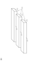
- FIG. 1 is a schematic perspective view of a semiconductor laser device according to the first embodiment.
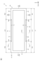
- FIG. 2 is a schematic plan view of the semiconductor laser device of FIG.
- FIG. 3 is a schematic cross-sectional view of the semiconductor laser device taken along line F3-F3 in FIG.
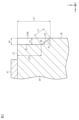
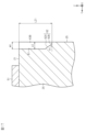
- FIG. 4 is a schematic enlarged cross-sectional view of the first recess and its periphery in the cross-sectional structure of the semiconductor laser device taken along line F4-F4 in FIG.
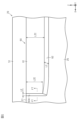
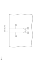
- FIG. 5 is a schematic side view of the first recess and its periphery.
- FIG. 6 is an enlarged view of the first end connection surface and its surroundings in the first recessed portion in FIG.
- FIG. 6 is an enlarged view of the first end connection surface and its surroundings in the first recessed portion in FIG.
- FIG. 7 is a schematic enlarged cross-sectional view of the first end connection surface and its periphery in the cross-sectional structure of the semiconductor laser device taken along line F7-F7 in FIG. 8A to 8C are schematic perspective views illustrating exemplary manufacturing processes for the semiconductor laser device of the first embodiment.
- FIG. 9 is a schematic perspective view showing an exemplary manufacturing process subsequent to FIG.
- FIG. 10 is a schematic perspective view showing an exemplary manufacturing process subsequent to FIG.
- FIG. 11 is a schematic perspective view showing an exemplary manufacturing process subsequent to FIG.
- FIG. 12 is a schematic plan view showing an exemplary manufacturing process subsequent to FIG. FIG.
- FIG. 13 is a schematic enlarged cross-sectional view of the separation groove and its periphery in the cross-sectional structure of the laser bar taken along line F13-F13 in FIG.
- FIG. 14 is a schematic perspective view of the semiconductor laser device according to the second embodiment.
- FIG. 15 is a schematic rear view of the semiconductor laser device of FIG.
- FIG. 16 is a schematic enlarged cross-sectional view of the first recess and its periphery in the cross-sectional structure of the semiconductor laser device taken along line F16-F16 in FIG.
- FIG. 17 is a schematic enlarged cross-sectional view of a first recess and its periphery in a semiconductor laser device according to a modified example.
- FIG. 18 is a side view of the semiconductor laser element of the modified example as viewed from the first end face.
- FIGS. 1 to 7 show the configuration of a semiconductor laser element 10
- FIGS. 8 to 13 show the manufacturing process of the semiconductor laser element 10.
- FIGS. Fig. 1 shows a schematic perspective structure of the semiconductor laser element 10.
- Fig. 2 shows a schematic planar structure of the semiconductor laser element 10.
- Fig. 3 is a cross-sectional structure of the semiconductor laser element 10 taken along line F3-F3 in Fig. 2, showing the internal configuration of the semiconductor laser element 10.
- the term "planar view” used in this disclosure refers to viewing the semiconductor laser element 10 in the Z direction of the mutually orthogonal XYZ axes shown in Fig. 1.
- the X direction is an example of a "first direction”
- the Y direction is an example of a "second direction”.
- the semiconductor laser element 10 is an edge-emitting laser diode, and includes an element body 20, and a front electrode 51 and a rear electrode 52 provided on the element body 20.
- the front electrode 51 constitutes the anode
- the rear electrode 52 constitutes the cathode.
- the element body 20 is formed into a rectangular parallelepiped shape with the Z direction being the thickness direction. Therefore, “plan view” also means viewing from the thickness direction of the element body 20.
- the element body 20 is formed into a rectangle with the X direction being the long side direction and the Y direction being the short side direction in plan view.
- the element body 20 has an element front surface 21 and an element back surface 22 that face opposite each other in the Z direction, a first end surface 23 and a second end surface 24 that face opposite each other in the X direction in a plan view, and a first side surface 25 and a second side surface 26 that face opposite each other in the Y direction in a plan view.
- the thickness direction (Z direction) of the element body 20 can be said to be the direction in which the element front surface 21 faces.
- the first end surface 23, the second end surface 24, the first side surface 25, and the second side surface 26 are located between the element front surface 21 and the element back surface 22 in the Z direction, and connect the element front surface 21 and the element back surface 22.
- the element body 20 is configured to emit light from the first end surface 23.
- the surface electrode 51 is formed on the element surface 21.
- the surface electrode 51 is formed in a rectangular plate shape with the thickness direction in the Z direction.
- the shape of the surface electrode 51 in a plan view is a rectangle with the X direction as the longitudinal direction and the Y direction as the lateral direction.
- the surface electrode 51 is formed to be one size smaller than the element body 20 in a plan view.
- the surface electrode 51 is formed of a laminated structure of multiple electrode films.
- the surface electrode 51 includes a first electrode film and a second electrode film formed on the first electrode film.
- the first electrode film is formed of, for example, a Ti (titanium)/Au (gold) alloy.
- the first electrode film is in contact with the surface 41 (element surface 21) of the semiconductor layer 40.
- the second electrode film is formed by, for example, Au plating.
- the back electrode 52 is formed on the back surface 22 of the element.
- the back electrode 52 is formed in a rectangular plate shape with the thickness direction in the Z direction.
- the shape of the back electrode 52 in a plan view is a rectangle with the X direction as the long side and the Y direction as the short side.
- the back electrode 52 is formed to be one size smaller than the element body 20 in a plan view. In other words, the back electrode 52 is the same size as the front electrode 51.
- the back electrode 52 is composed of a laminated structure of multiple electrode films.
- the back electrode 52 is formed of, for example, an AuGeNi (gold germanium nickel)/Ti/Au alloy.
- the back electrode 52 forms an ohmic contact with the semiconductor substrate 30.
- the element body 20 includes a semiconductor substrate 30 and a semiconductor layer 40 provided on the semiconductor substrate 30 .
- the semiconductor substrate 30 is formed in a rectangular plate shape with its thickness direction aligned in the Z direction.
- the semiconductor substrate 30 is formed in a rectangular shape with its longitudinal direction aligned in the X direction and its lateral direction aligned in the Y direction in a plan view.
- the semiconductor substrate 30 has a substrate front surface 31 and a substrate back surface 32 facing opposite each other in the Z direction, and a first substrate end surface 33, a second substrate end surface 34, a first substrate side surface 35, and a second substrate side surface 36 located between the substrate front surface 31 and the substrate back surface 32 in the Z direction and connecting the substrate front surface 31 and the substrate back surface 32.
- the substrate front surface 31 faces the same side as the element front surface 21, and the substrate back surface 32 faces the same side as the element back surface 22.
- the substrate back surface 32 constitutes the element back surface 22.
- the first substrate end surface 33 and the second substrate end surface 34 constitute both end surfaces in the X direction of the semiconductor substrate 30.
- first substrate end surface 33 and the second substrate end surface 34 face opposite each other in the X direction.
- the first substrate side surface 35 and the second substrate side surface 36 constitute both end surfaces in the Y direction of the semiconductor substrate 30. That is, the first substrate side surface 35 and the second substrate side surface 36 face opposite each other in the Y direction. Therefore, the first substrate end surface 33 faces the same side as the first end surface 23, and the second substrate end surface 34 faces the same side as the second end surface 24.
- the first substrate side surface 35 faces the same side as the first side surface 25, and the second substrate side surface 36 faces the same side as the second side surface 26.
- the first substrate end surface 33 constitutes a part of the first end surface 23 in the Z direction
- the second substrate end surface 34 constitutes a part of the second end surface 24 in the Z direction
- the first substrate side surface 35 constitutes a part of the first side surface 25 in the Z direction
- the second substrate side surface 36 constitutes a part of the second side surface 26 in the Z direction. Note that in FIG. 3, in order to show each component of the semiconductor layer 40, the overall thickness of the semiconductor layer 40 is shown as thick as the thickness of the semiconductor substrate 30, but in reality, the thickness of the semiconductor layer 40 is thinner than the thickness of the semiconductor substrate 30.
- the semiconductor substrate 30 is composed of an n-type semiconductor substrate (n-GaAs substrate) containing, for example, GaAs (gallium arsenide).
- the semiconductor substrate 30 contains at least one of, for example, Si (silicon), Te (tellurium), and Se (selenium) as n-type impurities.
- the angle of each of the first substrate side surface 35 and the second substrate side surface 36 with respect to the substrate surface 31 is 90°.
- the angle of each of the first substrate side surface 35 and the second substrate side surface 36 with respect to the substrate surface 31 being 90° also includes the angle of each of the first substrate side surface 35 and the second substrate side surface 36 with respect to the substrate surface 31 being 85° or more and 95° or less, taking into account the manufacturing error of the semiconductor substrate 30.
- the off-angle of the semiconductor substrate 30 is 0°.
- a just substrate is used for the semiconductor substrate 30.
- the surface orientation of the substrate surface 31 of the semiconductor substrate 30 is a (100) surface.
- the semiconductor layer 40 is formed on the substrate surface 31.
- the semiconductor layer 40 has a surface 41 that constitutes the element surface 21.
- the semiconductor layer 40 is epitaxially grown on the semiconductor substrate 30.
- the semiconductor layer 40 has a semiconductor layer stacking structure in which multiple semiconductor layers are stacked in the Z direction.
- each of the first substrate end face 33, the second substrate end face 34, the first substrate side face 35, and the second substrate side face 36 of the semiconductor substrate 30 is a (110) plane.
- the (110) plane of the semiconductor substrate 30 has a strong cleavage tendency.
- the first substrate end face 33 and the second substrate end face 34 of the semiconductor substrate 30 are composed of planes that are easier to cleave than the first substrate side face 35 and the second substrate side face 36.
- the semiconductor layer 40 includes an active layer 42, an n-side guide layer 43, a p-side guide layer 44, an n-type semiconductor layer 45, and a p-type semiconductor layer 46 as a plurality of semiconductor layers.
- a double heterojunction is formed by disposing the n-side guide layer 43 between the n-type semiconductor layer 45 and the active layer 42, and disposing the p-side guide layer 44 between the active layer 42 and the p-type semiconductor layer 46. Electrons are injected into the active layer 42 from the n-type semiconductor layer 45 via the n-side guide layer 43, and holes are injected from the p-type semiconductor layer 46 via the p-side guide layer 44. These electrons and holes are recombined in the active layer 42, so that laser light is generated in the active layer 42.
- the n-type semiconductor layer 45 includes an n-type cladding layer 45A formed on the semiconductor substrate 30.
- the n-type cladding layer 45A is disposed on the semiconductor substrate 30 side with respect to the active layer 42.
- the n-type cladding layer 45A is formed of a material containing, for example, AlGaAs (aluminum gallium arsenide).
- the n-type cladding layer 45A has a thickness of, for example, 20,000 ⁇ or more and 35,000 ⁇ or less.
- the n-type cladding layer 45A is formed of, for example, an Al x Ga (1-x) As (0 ⁇ x ⁇ 1) layer.
- the p-type semiconductor layer 46 includes a first p-type cladding layer 46A, a first p-type etching stop layer 46B, a second p-type cladding layer 46C, a second p-type etching stop layer 46D, a p-type cap layer 46E, and a p-type contact layer 46F, which are stacked on the p-side guide layer 44.
- both the first p-type cladding layer 46A and the second p-type cladding layer 46C are examples of "p-type cladding layers.”
- the first p-type cladding layer 46A and the second p-type cladding layer 46C are disposed on the opposite side of the active layer 42 to the n-type cladding layer 45A.
- Each of the first p-type cladding layer 46A and the second p-type cladding layer 46C is formed of a material containing, for example, AlGaAs.
- the first p-type cladding layer 46A has a thickness of, for example, 1000 ⁇ or more and 2000 ⁇ or less.
- the second p-type cladding layer 46C has a thickness of, for example, 8000 ⁇ or more and 12000 ⁇ or less.
- the thickness of the second p-type cladding layer 46C is thicker than the thickness of the first p-type cladding layer 46A.
- Each of the first p-type cladding layer 46A and the second p-type cladding layer 46C is formed of, for example, an Al x Ga (1-x) As (0 ⁇ x ⁇ 1) layer.
- the first p-type etching stop layer 46B and the second p-type etching stop layer 46D are each formed of a material containing, for example, InGaP (indium gallium phosphide).
- the thickness of each of the first p-type etching stop layer 46B and the second p-type etching stop layer 46D is thinner than the thickness of each of the first p-type cladding layer 46A and the second p-type cladding layer 46C.
- the first p-type etching stop layer 46B has a thickness of, for example, 50 ⁇ or more and 300 ⁇ or less.
- the second p-type etching stop layer 46D has a thickness of, for example, 50 ⁇ or more and 300 ⁇ or less.
- the p-type cap layer 46E is formed of a material containing, for example, GaAs.
- the thickness of the p-type cap layer 46E is, for example, thicker than the thickness of each of the first p-type etching stop layer 46B and the second p-type etching stop layer 46D, and thinner than the thickness of each of the first p-type cladding layer 46A and the second p-type cladding layer 46C.
- the p-type cap layer 46E has a thickness of, for example, 1000 ⁇ or more and 3000 ⁇ or less.
- the p-type contact layer 46F is a low resistance layer for forming an ohmic contact with the front electrode 51.
- the p-type contact layer 46F is formed as a p-type semiconductor layer, for example, in which Be (beryllium) is implanted as a p-type dopant into GaAs.
- the thickness of the p-type contact layer 46F is thicker than the thicknesses of the first p-type cladding layer 46A, the first p-type etching stop layer 46B, the second p-type cladding layer 46C, the second p-type etching stop layer 46D, and the p-type cap layer 46E.
- the p-type contact layer 46F has a thickness of, for example, 30,000 ⁇ or more and 60,000 ⁇ or less.
- the n-type cladding layer 45A and the first and second p-type cladding layers 46A and 46C are configured to confine carriers (electrons and holes) in the active layer 42 and confine laser light from the active layer 42 between the n-type cladding layer 45A and the first and second p-type cladding layers 46A and 46C.
- the n-type cladding layer 45A is formed as an n-type semiconductor layer in which, for example, Si (silicon) is injected into AlGaAs as an n-type dopant.
- Each of the first and second p-type cladding layers 46A and 46C is formed as a p-type semiconductor layer in which, for example, Be is injected into AlGaAs as a p-type dopant.
- the n-type cladding layer 45A has a larger band gap than the n-side guide layer 43.
- the first p-type cladding layer 46A and the second p-type cladding layer 46C have a larger band gap than the p-side guide layer 44. This enhances the effect of confining carriers in the active layer 42 and the effect of confining laser light from the active layer 42 between the n-type cladding layer 45A and the first p-type cladding layer 46A and the second p-type cladding layer 46C, respectively, thereby realizing a highly efficient semiconductor laser element 10.
- Each of the n-side guide layer 43 and the p-side guide layer 44 is formed of a material containing AlGaAs.
- Each of the n-side guide layer 43 and the p-side guide layer 44 has a thickness of, for example, 200 ⁇ or more and 500 ⁇ or less.
- the n-side guide layer 43 is laminated on the n-type semiconductor layer 45.
- the p-side guide layer 44 is laminated on the active layer 42.
- Each of the n-side guide layer 43 and the p-side guide layer 44 is formed of, for example, an Al x Ga (1-x) As (0 ⁇ x ⁇ 1) layer.
- the active layer 42 has a multiple-quantum well (MQW) structure.
- the active layer 42 is a layer that generates laser light by the recombination of electrons and holes and amplifies the generated laser light.
- the active layer 42 is formed by repeatedly laminating, for example, quantum well layers made of undoped GaAsP layers and barrier layers made of undoped InAlGaAs layers, alternating over multiple periods.
- the ridge portion 47 is formed by removing a portion of each of the second p-type cladding layer 46C, the second p-type etching stop layer 46D, and the p-type cap layer 46E in the p-type semiconductor layer 46.
- the ridge portion 47 is formed in a substantially trapezoidal (mesa) shape in the cross section shown in FIG. 3 by removing a portion of the second p-type cladding layer 46C, the second p-type etching stop layer 46D, and the p-type cap layer 46E by etching.
- a current confinement layer 48 is formed on the side of the ridge portion 47.
- the side of the p-type cap layer 46E, the side of the second p-type etching stop layer 46D, the exposed surface of the second p-type cladding layer 46C, and the exposed surface of the first p-type etching stop layer 46B are covered with the current confinement layer 48.
- the current confinement layer 48 and the exposed surface of the p-type cap layer 46E are covered with the p-type contact layer 46F.
- a Fabry-Perot resonator is formed by the n-side guide layer 43, the active layer 42, and the p-side guide layer 44, with the first end face 23 and the second end face 24 (see FIG. 1 for both) as the resonator end faces. More specifically, the laser light generated in the active layer 42 is amplified by stimulated emission while traveling back and forth between the first end face 23 and the second end face 24. Then, a part of the amplified laser light is emitted as laser light from the first end face 23 and the second end face 24.
- an end face film (not shown) is formed on the first end face 23 and the second end face 24. This end face film may include a reflective film having insulating properties.
- the end face film may include an anti-reflection film (AR coat) having insulating properties.
- AR coat anti-reflection film
- the reflectance of the end face film including the reflective film may be adjusted.
- a reflective film may be formed that is fired so that the first end face 23 mainly emits laser light and the second end face 24 emits almost no laser light.
- FIGS. Fig. 4 is a cross-sectional view of the semiconductor laser device 10 taken along line F4-F4 in Fig. 2, showing an enlarged cross-sectional view of a portion of each of the device surface 21 and the first side surface 25 of the device body 20.
- Fig. 5 shows an enlarged view of a first recessed portion 60, which will be described later.
- Fig. 6 shows an enlarged view of a portion of the first recessed portion 60 in Fig. 5.
- Fig. 7 shows a cross-sectional view of the first recessed portion 60 taken along line F7-F7 in Fig. 6.
- the element body 20 includes a first recessed portion 60 and a second recessed portion 70.
- the first recessed portion 60 is provided between the first side surface 25 and the element surface 21 of the element body 20.
- the first recessed portion 60 is recessed toward the inside of the element body 20.
- the first recessed portion 60 opens in the direction in which the element surface 21 faces and also opens in the direction in which the first side surface 25 faces.
- the second recessed portion 70 is provided between the second side surface 26 and the element surface 21 of the element body 20.
- the second recessed portion 70 is recessed toward the inside of the element body 20.
- the second recessed portion 70 opens in the direction in which the element surface 21 faces and also opens in the direction in which the second side surface 26 faces.
- the first recessed portion 60 and the second recessed portion 70 are provided in a part of the element body 20 closer to the element surface 21, including the element surface 21, in the Z direction.
- the first recess 60 and the second recess 70 are formed from the semiconductor layer 40 to the semiconductor substrate 30. More specifically, the first recess 60 and the second recess 70 are formed throughout the semiconductor layer 40 in the Z direction.
- the first recess 60 and the second recess 70 are formed in a portion of the semiconductor substrate 30 closer to the semiconductor layer 40 in the Z direction.
- the first recessed portion 60 includes a first inner side surface 61 facing the same side as the first side surface 25 , and a first connecting surface 62 connecting the first inner side surface 61 and the first side surface 25 .
- the first inner side surface 61 is formed at a position closer to the second side surface 26 than the first side surface 25 in the Y direction.
- the first inner side surface 61 is connected to the element surface 21.
- the first inner side surface 61 penetrates the semiconductor layer 40 (see FIG. 3 ) in the Z direction.
- the first inner side surface 61 is provided in a part of the semiconductor substrate 30 closer to the semiconductor layer 40 in the Z direction.
- the first inner side surface 61 is a surface parallel to the first side surface 25.
- the first connection surface 62 is formed at a position closer to the element back surface 22 than the first inner surface 61. In other words, the first connection surface 62 is provided closer to the element back surface 22 than the semiconductor layer 40. In other words, the first connection surface 62 is provided on the semiconductor substrate 30 (see FIG. 3).
- the first connection surface 62 is connected to the edge closer to the element back surface 22 of both end edges of the first inner surface 61 in the Z direction. In one example, the first connection surface 62 is connected over the entire edge of the first inner surface 61 in the X direction.
- the first connection surface 62 is formed as an inclined surface that is inclined at an angle different from the first side surface 25 and the second side surface 26 with respect to the element surface 21. More specifically, the first connection surface 62 is inclined toward the first side surface 25 as it moves from the first inner surface 61 toward the element back surface 22 in the Z direction.
- the angle ⁇ 1 of the first connection surface 62 with respect to the element surface 21 is 45° or more and 65° or less.
- the angle ⁇ 1 is 50° or more and 60° or less.
- the length LC in the inclination direction of the first connection surface 62 is shorter than the length LZC of the first inner surface 61 in the Z direction.
- the length LC is shorter than the length LZE in the Z direction at the end of the first inner surface 61 in the X direction (see FIG. 6).
- the length LC is 2 ⁇ m or more and 8 ⁇ m or less.
- the distance W1 between the first side surface 25 and the first inner surface 61 in the direction perpendicular to the first side surface 25 is shorter than the length LX1 of the first recessed portion 60 in the X direction (see FIG. 2).
- the distance W1 is shorter than the length LZ1 of the first recessed portion 60 in the Z direction.
- the distance W1 is shorter than the length LZC of the first inner surface 61 in the Z direction.
- the distance W1 is shorter than the length LC of the first connecting surface 62 in the inclination direction.
- the distance W1 is 1 ⁇ m or more and 5 ⁇ m or less.
- the first connection surface 62 is inclined toward the element surface 21 at both ends in the X direction as it approaches the edge in the X direction.
- the end of the first connection surface 62 in the X direction that is closer to the first end surface 23 (see FIG. 2) is curved toward the element surface 21 as it approaches the edge in the X direction. Therefore, the Z-direction length LZE of both ends of the first inner surface 61 in the X direction is shorter than the Z-direction length LZC of the portion of the first inner surface 61 closer to the center than both ends in the X direction.
- the end of the first connection surface 62 in the X direction that is closer to the second end surface 24 (see FIG. 2) may have the same configuration as the end of the first connection surface 62 in the X direction that is closer to the first end surface 23.
- the first recess 60 includes first end connection surfaces 63A, 63B formed at both ends in the X direction.
- the first end connection surface 63A connects the end of the first inner surface 61 in the X direction that is closer to the first end surface 23 (see FIG. 2) to the first side surface 25.
- the first end connection surface 63B connects the end of the first inner surface 61 in the X direction that is closer to the second end surface 24 (see FIG. 2) to the first side surface 25.
- the first end connection surface 63A connects the element surface 21 and the first connection surface 62 in the Z direction. In one example, the first end connection surface 63A extends along the Z direction. In one example, the first end connection surface 63A is a surface that is perpendicular to the element surface 21.
- the angle ⁇ 2 of the first end connection surface 63A relative to the first inner surface 61 is greater than the angle ⁇ A (see FIG. 4) of the first connection surface 62 relative to the first inner surface 61.
- the angle ⁇ 2 is greater than or equal to 85° and less than or equal to 95°.
- the angle ⁇ 2 is greater than or equal to 87° and less than or equal to 93°.
- the angle ⁇ 2 is greater than or equal to 88° and less than or equal to 92°.
- the angle ⁇ 2 is greater than or equal to 89° and less than or equal to 91°. In the example shown in FIG. 7, the angle ⁇ 2 is 90°.
- the length LE of the first end connection surface 63A between the first inner surface 61 and the first side surface 25 is shorter than the length LC (see Figure 6) of the first connection surface 62 in the inclination direction.
- the length LE is 1 ⁇ m or more and 5 ⁇ m or less.
- the first end connection surface 63B has the same configuration as the first end connection surface 63A. Therefore, the angle of the first end connection surface 63B with respect to the first inner surface 61 is the same as the angle ⁇ 2.
- the length of the first end connection surface 63B between the first inner surface 61 and the first side surface 25 is equal to the length LE.
- the second recessed portion 70 includes a second inner side surface 71 facing the same side as the second side surface 26, and a second connection surface 72 connecting the second inner side surface 71 and the second side surface 26.
- the second connection surface 72 is formed as an inclined surface inclined at an angle different from that of the first side surface 25 and the second side surface 26 with respect to the element surface 21.
- the second recessed portion 70 includes second end connection surfaces 73A, 73B formed at both ends in the X direction.
- the second end connection surface 73A connects the end of the second inner side surface 71 closer to the first end surface 23 to the second side surface 26 among both ends in the X direction.
- the second end connection surface 73B connects the end of the second inner side surface 71 closer to the second end surface 24 to the second side surface 26 among both ends in the X direction.
- the shape and size of the second recess 70 are the same as those of the first recess 60. That is, the angle of the second connection surface 72 with respect to the element surface 21 is the same as the angle ⁇ 1 of the first connection surface 62 with respect to the element surface 21. That is, the angle of the second connection surface 72 with respect to the element surface 21 is 50° or more and 60° or less. Preferably, the angle of the second connection surface 72 with respect to the element surface 21 is 53° or more and 57° or less.
- the distance between the second side surface 26 and the second inner surface 71 in a direction perpendicular to the second side surface 26 (Y direction in the first embodiment) is equal to the distance W1.
- the distance between the second side surface 26 and the second inner surface 71 in a direction perpendicular to the second side surface 26 is 1 ⁇ m or more and 5 ⁇ m or less.
- the angle of the second end connection surfaces 73A, 73B with respect to the second inner surface 71 is equal to the angle ⁇ 2 of the first end connection surface 63A with respect to the first inner surface 61. Therefore, the angle of the second end connection surfaces 73A, 73B with respect to the second inner side surface 71 is larger than the angle of the second connection surface 72 with respect to the second inner side surface 71.
- the angle of the second end connection surfaces 73A, 73B with respect to the second inner side surface 71 may be, for example, 85° or more and 95° or less, for example, 87° or more and 93° or less, for example, 88° or more and 92° or less, or for example, 89° or more and 91° or less.
- the length of the second end connection surfaces 73A, 73B between the second inner side surface 71 and the second side surface 26 is equal to the length LE of the first end connection surface 63A between the first inner side surface 61 and the first side surface 25.
- the length of the second end connection surfaces 73A, 73B between the second inner side surface 71 and the second side surface 26 is shorter than the length of the second connection surface 72 in the inclination direction.
- the length of the second end connection surfaces 73A, 73B between the second inner surface 71 and the second side surface 26 may be, for example, 1 ⁇ m or more and 5 ⁇ m or less.
- the first recess 60 and the second recess 70 are provided partially in the element body 20 in the X direction.
- the element body 20 includes a first region 27 and a second region 28 at both ends in the X direction.
- the first region 27 is formed at both ends in the X direction of the first side surface 25 of the element body 20.
- the second region 28 is formed at both ends in the X direction of the second side surface 26 of the element body 20.
- the first recessed portion 60 is provided between the first regions 27 formed at both ends in the X direction of the element body 20.
- the second recessed portion 70 is provided between the second regions 28 formed at both ends in the X direction of the element body 20.
- one first recessed portion 60 is provided between the first regions 27 formed at both ends in the X direction of the element body 20.
- One second recessed portion 70 is provided between the second regions 28 formed at both ends in the X direction of the element body 20. In this manner, each of the first recess 60 and the second recess 70 is provided in the element body 20 at a position spaced apart from both the first end face 23 and the second end face 24 in the X direction.
- the X-direction lengths LX1, LX2 of the first recess 60 and the second recess 70 are longer than the X-direction length RX1 of the first region 27 and the X-direction length RX2 of the second region 28. Furthermore, each of the lengths LX1, LX2 is longer than the sum of the lengths RX1 and RX2 (RX1+RX2). In other words, the lengths LX1, LX2 are longer than 1/2 the X-direction length LS of the element body 20. Furthermore, in one example, the X-direction length LX1 of the first recess 60 is equal to the X-direction length LX2 of the second recess 70.
- the lengths RX1 in the X direction of the two first regions 27 are equal to each other.
- the lengths RX2 in the X direction of the two second regions 28 are equal to each other.
- the lengths RX1 and RX2 are equal to each other. Note that the lengths RX1 and RX2 can be changed arbitrarily. In one example, the lengths RX1 in the X direction of the two first regions 27 may be different from each other. In one example, the lengths RX2 in the X direction of the two second regions 28 may be different from each other. In one example, the lengths RX1 and RX2 may be different from each other.
- the ratio (LX1/LS) of the X-direction length LX1 of the first recessed portion 60 to the X-direction length LS of the element body 20, and the ratio (LX2/LS) of the X-direction length LX2 of the second recessed portion 70 to the X-direction length LS of the element body 20 are each 5/8 or more and 7/8 or less.
- each of the ratios (LX1/LS) and (LX2/LS) may be 4/6 or more and 5/6 or less.
- the X-direction lengths LX1, LX2 of the first recessed portion 60 and the second recessed portion 70 are approximately 400 ⁇ m.
- the X-direction length RX1 of the first region 27 is approximately 100 ⁇ m.
- the X-direction length RX2 of the second region 28 is approximately 100 ⁇ m. Therefore, the X-direction length LS of the element body 20 is approximately 600 ⁇ m.
- the ratio (LX1/LS) of the X-direction length LX1 of the first recessed portion 60 to the X-direction length LS of the element body 20, and the ratio (LX2/LS) of the X-direction length LX2 of the second recessed portion 70 to the X-direction length LS of the element body 20 are each 2/3.
- the length LZ1 of the first recess 60 in the Z direction is shorter than the length LX1 of the first recess 60 in the X direction.
- the length LZ1 can be defined as the distance between the element surface 21 and the boundary between the first connection surface 62 and the first side surface 25 in the Z direction.
- the boundary between the first connection surface 62 and the first side surface 25 is the portion where the first connection surface 62 and the first side surface 25 are connected in the Z direction.
- the length of the second recess 70 in the Z direction is shorter than the length LX2 of the second recess 70 in the X direction.
- the length of the second recess 70 in the Z direction can be defined by the distance between the element surface 21 and the boundary between the second connection surface 72 and the second side surface 26 in the Z direction.
- the boundary between the second connection surface 72 and the second side surface 26 is the portion where the second connection surface 72 and the second side surface 26 are connected in the Z direction.
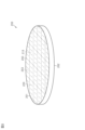
- FIG. 8 shows a schematic perspective structure of a semiconductor wafer 200 .
- the manufacturing method of the semiconductor laser element 10 includes a step of preparing a semiconductor wafer 200.
- the semiconductor wafer 200 is made of GaAs.
- the semiconductor wafer 200 includes a wafer constituting a plurality of semiconductor substrates 30 (see FIG. 1) and a semiconductor layer stacking structure constituting a semiconductor layer 40 (see FIG. 1) on each semiconductor substrate 30.
- the semiconductor wafer 200 includes a wafer front surface 201 and a wafer back surface 202 facing opposite sides to each other in the Z direction.
- the wafer front surface 201 constitutes a (100) surface.
- a plurality of front surface electrodes 51 are formed on the wafer front surface 201.
- a plurality of back surface electrodes 52 are formed on the wafer back surface 202.
- a semiconductor wafer 200 has a plurality of laser bars (LD bars) 210 formed thereon, each of which includes a plurality of individual elements.
- Each laser bar 210 is formed in a rectangular region defined by imaginary cutting lines 203 on the semiconductor wafer 200.
- Each individual element constitutes a semiconductor laser element 10 (see FIG. 1).
- the laser bar 210 includes a plurality of semiconductor laser elements 10. This laser bar 210 may be referred to as a bar-shaped body or a base substrate.
- the manufacturing method of the semiconductor laser element 10 includes a step of dividing the semiconductor wafer 200 along the cutting line 203.
- the semiconductor wafer 200 is scratched along the cutting line 203 using a diamond cutter.
- the semiconductor wafer 200 is divided by applying force to the wafer back surface 202 of the semiconductor wafer 200.
- This step forms a plurality of rod-shaped laser bars 210 having a longitudinal direction and a lateral direction, as shown in FIG. 9.
- FIG. 9 shows a schematic perspective structure of three laser bars 210. Note that the front electrode 51, the back electrode 52, and the separation groove 220 described later are omitted in FIG. 9.
- the laser bars 210 may be formed by cutting out a plate-shaped substrate including a plurality of laser bars 210 from the semiconductor wafer 200 and then cleaving the plate-shaped substrate.
- the cutting out of the plate-shaped substrate may be performed by dicing, scribing, laser processing, or the like.
- each laser bar 210 constitutes the first end surface 23 (second end surface 24) of the semiconductor laser element 10 shown in FIG. 1.
- the lateral side surface 212 of each laser bar 210 constitutes the first side surface 25 (second side surface 26) of the semiconductor laser element 10 shown in FIG. 1.
- FIG. 10 shows a stacked structure of laser bars 210 and separators 230 .
- the method for manufacturing the semiconductor laser element 10 includes a step of alternately stacking a plurality of laser bars 210 and a plurality of separators 230 one by one, and a step of forming an end face film.
- the end face film may include a reflective film having insulating properties.
- the end face film may also include an anti-reflection film (AR coat) having insulating properties.
- the end face film including the reflective film may have an adjusted reflectance.
- a sintered reflective film may be formed so that the side surface 211 constituting the first end face 23 mainly emits laser light, and almost no laser light is emitted from the side surface 211 constituting the second end face 24.
- FIG. 11 shows the perspective structure of one laser bar 210.
- FIG. 12 shows the planar structure of one laser bar.
- FIG. 13 shows a portion of the cross-sectional structure of the laser bar 210 cut along line F13-F13 in FIG. 12.
- the method for manufacturing the semiconductor laser element 10 includes a step of forming a separation groove 220. This step is carried out, for example, before dividing the semiconductor wafer 200 into a plurality of laser bars 210. Note that, when a plate-like substrate including a plurality of laser bars 210 is cut out from the semiconductor wafer 200, the step of forming the separation groove 220 may be carried out before cutting out the plate-like substrate. In other words, the separation groove 220 is formed in the semiconductor wafer 200.
- each separation groove 220 extends along the short side direction of the laser bar 210.
- Each separation groove 220 is provided partially in the short side direction of the laser bar 210.
- each separation groove 220 is provided at intervals from both side surfaces 211 of the laser bar 210.
- the portions between the separation grooves 220 and the side surfaces 211 in the short side direction of the laser bar 210 constitute a first region 27 and a second region 28 (see Figure 2).
- each separation groove 220 is formed from the semiconductor layer 40 (semiconductor layer stacking structure) to the semiconductor wafer 200.
- Each separation groove 220 penetrates the semiconductor layer 40 (semiconductor layer stacking structure) in the Z direction.
- Each separation groove 220 is formed from the wafer surface 201 of the semiconductor wafer 200 to a part in the Z direction.
- Each separation groove 220 is formed by etching. In one example, each separation groove 220 is formed by dry etching.
- the separation groove 220 is a groove that constitutes the first recessed portion 60 and the second recessed portion 70.
- the tip of the separation groove 220 is formed in a tapered shape that tapers toward the tip.
- the separation groove 220 includes a first separation side surface 221 that constitutes the first inner side surface 61, a second separation side surface 222 that constitutes the second inner side surface 71, a first tapered surface 223 that constitutes the inclined surface 62A of the first connecting surface 62, and a second tapered surface 224 that constitutes the inclined surface of the second connecting surface 72.
- the first tapered surface 223 and the second tapered surface 224 are connected to form the tapered shape of the separation groove 220.
- the first tapered surface 223 and the second tapered surface 224 constitute a (111) plane.
- the method for manufacturing the semiconductor laser device 10 includes a step of dividing the laser bar 210 into a plurality of semiconductor laser devices 10 .
- the laser bar 210 is cleaved along the separation grooves 220.
- an external stress is applied to the laser bar 210 with a blade (not shown) in contact with the back surface side of the laser bar 210 along each separation groove 220.
- cracks are generated in the laser bar 210 starting from the tip of each separation groove 220, and the laser bar 210 is divided along each separation groove 220.
- the semiconductor laser device 10 is manufactured.
- the width and depth of the separation grooves may vary.
- the laser bar 210 is cleaved, cracks are generated in the laser bar 210 starting from multiple points in the separation grooves, resulting in wrinkles being formed on the first side surface 25 of the semiconductor laser elements 10.
- mechanical contact of the diamond cutter with the semiconductor wafer 200 may cause the semiconductor wafer 200 to chip away at the portion where the separation groove is to be formed, resulting in chip pieces being scattered off. Such chip pieces may become foreign matter and adhere to the first end face 23 and the second end face 24 of the semiconductor laser element 10 after separation.
- separation grooves for dividing the laser bar 210 into multiple semiconductor laser elements 10 by laser processing instead of using a diamond cutter, the separation grooves and their surroundings will melt due to the heat of the laser. Laser processing may also cause variations in the width and depth of the separation grooves.
- the laser bar 210 is cleaved, cracks will form in the laser bar 210 starting from multiple points in the separation grooves, resulting in wrinkles being formed on the first side surface 25 of the semiconductor laser elements 10.
- a separation groove 220 for dividing the laser bar 210 into a plurality of semiconductor laser elements 10 is formed by dry etching.
- dry etching a first separation side 221 and a second separation side 222 of the separation groove 220 are formed along the surface orientation of the laser bar 210. That is, the first separation side 221 and the second separation side 222 are (110) surfaces.
- the first tapered surface 223 and the second tapered surface 224 are (111) surfaces. Therefore, the depth of the separation groove 220 is unlikely to vary. Therefore, even if the laser bar 210 is cleaved, the formation of wrinkles on the first side 25 of the semiconductor laser element 10 can be suppressed.
- the semiconductor laser element 10 includes an element body 20 having an element front surface 21 and an element back surface 22 facing opposite sides to each other, a first end surface 23 and a second end surface 24 facing opposite sides to each other in the X direction in a plan view, and a first side surface 25 and a second side surface 26 facing opposite sides to each other in the Y direction, and emitting laser light from the first end surface 23, a front surface electrode 51 formed on the element front surface 21, and a back surface electrode 52 formed on the element back surface 22.
- the element body 20 includes a first recessed portion 60 provided between the first side surface 25 and the element front surface 21 and recessed toward the inside of the element body 20, and a second recessed portion 70 provided between the second side surface 26 and the element front surface 21 and recessed toward the inside of the element body 20.
- the first recessed portion 60 includes a first inner side surface 61 facing the same side as the first side surface 25, and a first connection surface 62 connecting the first inner side surface 61 and the first side surface 25.
- the second recess 70 includes a second inner side surface 71 facing the same side as the second side surface 26, and a second connection surface 72 connecting the second inner side surface 71 and the second side surface 26.
- Each of the first connection surface 62 and the second connection surface 72 includes an inclined surface that is inclined at an angle different from that of the first side surface 25 and the second side surface 26 with respect to the element surface 21.
- the first connecting surface 62 and the second connecting surface 72 serving as inclined surfaces can suppress the occurrence of wrinkles on the first side surface 25 and the second side surface 26. Therefore, the quality of the first side surface 25 and the second side surface 26, which become the cleavage surfaces, can be improved.
- the angle ⁇ 1 of the first connecting surface 62 with respect to the element surface 21 and the angle of the second connecting surface 72 with respect to the element surface 21 are each equal to or greater than 50° and equal to or less than 60°.
- This configuration can further suppress the occurrence of wrinkles on the first side surface 25 and the second side surface 26 when the semiconductor laser device 10 is formed by cleaving the laser bar 210. Therefore, the quality of the first side surface 25 and the second side surface 26, which become the cleavage planes, can be improved.
- Each of the first recess 60 and the second recess 70 is provided partially in the element body 20 in the X direction. According to this configuration, the laser bar 210 is less likely to crack when handled, compared to a configuration in which the first recessed portion 60 and the second recessed portion 70 are each provided over the entire element body 20 in the X direction. Therefore, the laser bar 210 can be handled more easily.
- the element body 20 includes a first region 27 in which the first recessed portion 60 is not formed at both ends in the X direction in the portion between the first side surface 25 and the element surface 21, and a second region 28 in which the second recessed portion 70 is not formed at both ends in the X direction in the portion between the second side surface 26 and the element surface 21.
- One first recessed portion 60 is provided between the first regions 27 at both ends in the X direction in the portion between the first side surface 25 and the element surface 21.
- One second recessed portion 70 is provided between the second regions 28 at both ends in the X direction in the portion between the second side surface 26 and the element surface 21.
- the laser bar 210 is less likely to crack when handled compared to when the first recessed portion 60 is provided at the end in the X direction of the portion between the first side surface 25 and the element surface 21, and when the second recessed portion 70 is provided at the end in the X direction of the portion between the second side surface 26 and the element surface 21. Therefore, the laser bar 210 is easier to handle.
- the X-direction length LX1 of the first recessed portion 60 is longer than the X-direction length RX1 of the first region 27.
- the X-direction length LX2 of the second recessed portion 70 is longer than the X-direction length RX2 of the second region 28.
- the X-direction length LX1 of the first recess 60 is shorter than the X-direction length RX1 of the first region 27, and the X-direction length LX2 of the second recess 70 is shorter than the X-direction length RX2 of the second region 28, making it easier to cleave the laser bar 210.
- the ratio (LX1/LS) of the X-direction length LX1 of the first recessed portion 60 to the X-direction length LS of the element body 20, and the ratio (LX2/LS) of the X-direction length LX2 of the second recessed portion 70 to the X-direction length LS of the element body 20 are each 5/8 or more and 7/8 or less.
- This configuration makes it possible to achieve both easier handling of the laser bar 210 by making the laser bar 210 less likely to crack when handling the laser bar 210, and easier cleavage of the laser bar 210.
- the first recessed portion 60 includes first end connection surfaces 63A, 63B formed at both ends in the X direction.
- the second recessed portion 70 includes second end connection surfaces 73A, 73B formed at both ends in the X direction.
- the angle ⁇ 2 of the first end connection surfaces 63A, 63B relative to the first inner surface 61 and the angle of the second end connection surfaces 73A, 73B relative to the second inner surface 71 are each greater than the angle ⁇ A of the first connection surface 62 relative to the first inner surface 61 and the angle of the second connection surface 72 relative to the second inner surface 71.
- the laser bar 210 is less likely to crack when handled compared to when the angle ⁇ 2 of the first end connection surfaces 63A, 63B relative to the first inner side surface 61 and the angle of the second end connection surfaces 73A, 73B relative to the second inner side surface 71 are less than the angle ⁇ A of the first connection surface 62 relative to the first inner side surface 61 and the angle of the second connection surface 72 relative to the second inner side surface 71. Therefore, the laser bar 210 is easier to handle.
- the angle ⁇ 2 of the first end connection surfaces 63A, 63B relative to the first inner surface 61 and the angle of the second end connection surfaces 73A, 73B relative to the second inner surface 71 are each 85° or more and 95° or less.
- the laser bar 210 is less likely to crack when handled compared to when the angle ⁇ 2 of the first end connection surfaces 63A, 63B relative to the first inner surface 61 and the angle of the second end connection surfaces 73A, 73B relative to the second inner surface 71 are each less than 85° or greater than 95°. Therefore, the laser bar 210 is easier to handle.
- the angle ⁇ 2 of the first end connection surfaces 63A, 63B relative to the first inner surface 61 and the angle of the second end connection surfaces 73A, 73B relative to the second inner surface 71 are each 87° or more and 93° or less.
- the laser bar 210 is less likely to crack when handled compared to when the angle ⁇ 2 of the first end connection surfaces 63A, 63B relative to the first inner surface 61 and the angle of the second end connection surfaces 73A, 73B relative to the second inner surface 71 are each less than 87° or greater than 93°. Therefore, the laser bar 210 is easier to handle.
- the angle ⁇ 2 of the first end connection surfaces 63A, 63B relative to the first inner surface 61 and the angle of the second end connection surfaces 73A, 73B relative to the second inner surface 71 are each 88° or more and 92° or less.
- the laser bar 210 is less likely to crack when handled compared to when the angle ⁇ 2 of the first end connection surfaces 63A, 63B relative to the first inner surface 61 and the angle of the second end connection surfaces 73A, 73B relative to the second inner surface 71 are each less than 88° or greater than 92°. Therefore, the laser bar 210 is easier to handle.
- the first recessed portion 60 includes first end connection surfaces 63A, 63B formed at both ends in the X direction.
- the second recessed portion 70 includes second end connection surfaces 73A, 73B formed at both ends in the X direction.
- the length LE of the first end connection surfaces 63A, 63B between the first inner surface 61 and the first side surface 25 and the length of the second end connection surfaces 73A, 73B between the second inner surface 71 and the second side surface 26 are each shorter than the length LC of the first connection surface 62 in the inclination direction and the length of the second connection surface 72 in the inclination direction.
- the laser bar 210 is less likely to crack when handled. Therefore, the laser bar 210 is easier to handle.
- the separation groove 220 that constitutes the first recess 60 and the second recess 70 is formed by removing the semiconductor layer 40 and the semiconductor substrate 30 of the element body 20 using dry etching.
- the width and depth of the separation groove 220 are less likely to vary compared to when the first recess 60 and the second recess 70 are formed using a diamond cutter or laser processing. Therefore, even when the laser bar 210 is cleaved, the formation of wrinkles on the first side surface 25 of the semiconductor laser element 10 can be suppressed.
- the semiconductor laser device 10 of the second embodiment will be described with reference to Figures 14 to 16.
- the semiconductor laser device 10 of the second embodiment differs from the semiconductor laser device 10 of the first embodiment mainly in the positions at which the first recessed portion 60 and the second recessed portion 70 are formed.
- components common to the semiconductor laser device 10 of the first embodiment are denoted by the same reference numerals, and descriptions thereof will be omitted.
- FIG. 14 shows a schematic perspective structure of the semiconductor laser element 10 of the second embodiment.
- FIG. 15 shows a schematic planar structure of the semiconductor laser element 10 of FIG. 14 on the back surface 22 side.
- FIG. 16 shows a cross-sectional structure of the semiconductor laser element 10 cut along line F16-F16 in FIG. 15, and shows an enlarged cross-sectional structure of the first recessed portion 60 and its surroundings.
- the first recess 60 is provided between the first side surface 25 and the rear surface 22 of the element body 20.
- the second recess 70 is provided between the second side surface 26 and the rear surface 22 of the element body 20.
- the first recess 60 and the second recess 70 are recessed toward the inside of the element body 20.
- the first recess 60 and the second recess 70 are provided in the semiconductor substrate 30.
- the first recess 60 and the second recess 70 are not provided in the semiconductor layer 40.
- the first recess 60 includes a first inner surface 61 facing the same side as the first side surface 25 , and a first connecting surface 62 connecting the first inner surface 61 and the first side surface 25 .
- the first inner side surface 61 is connected to the element back surface 22.
- the first inner side surface 61 is formed in a part of the element body 20 closer to the element back surface 22 in the Z direction. More specifically, the first inner side surface 61 is formed in a part of the semiconductor substrate 30 closer to the substrate back surface 32 in the Z direction.
- the first inner side surface 61 is a surface parallel to the first side surface 25.
- the first connection surface 62 is formed at a position closer to the element surface 21 than the first inner surface 61.
- the first connection surface 62 is formed as an inclined surface that is inclined at an angle different from the first side surface 25 and the second side surface 26 with respect to the element back surface 22. More specifically, the first connection surface 62 is inclined toward the first side surface 25 as it moves from the first inner surface 61 toward the element front surface 21 in the Z direction.
- the angle ⁇ 3 of the first connection surface 62 with respect to the element back surface 22 is 50° or more and 60° or less. Preferably, the angle ⁇ 3 is 53° or more and 57° or less.
- the length LC of the first connection surface 62 in the inclination direction is shorter than the length of the first inner surface 61 in the Z direction. This length LC is, for example, the same as the length LC of the first embodiment.
- the distance W1 between the first side surface 25 and the first inner side surface 61 in the direction perpendicular to the first side surface 25 is the same as the distance W1 in the first embodiment (see FIG. 4).
- the distance W1 is 1 ⁇ m or more and 5 ⁇ m or less.
- the first recess 60 includes first end connection surfaces 63A, 63B formed at both ends in the X direction.
- the first end connection surfaces 63A, 63B are connected to the element rear surface 22.
- the shape and size of the first end connection surfaces 63A, 63B in the second embodiment are the same as those in the first embodiment. Therefore, the angle of the first end connection surface 63A relative to the first inner surface 61 is the same as the angle ⁇ 2 shown in FIG. 7. Therefore, the angle of the first end connection surface 63A relative to the first inner surface 61 is larger than the angle ⁇ B of the first connection surface 62 relative to the first inner surface 61.
- the angle of the first end connection surface 63A relative to the first inner surface 61 is 85° or more and 95° or less. In one example, the angle of the first end connection surface 63A relative to the first inner surface 61 is 87° or more and 93° or less. In one example, the angle of the first end connection surface 63A relative to the first inner surface 61 is 88° or more and 92° or less. In one example, the angle of the first end connection surface 63A relative to the first inner surface 61 is 89° or more and 91° or less.
- the first end connection surface 63B has the same configuration as the first end connection surface 63A.
- the second recessed portion 70 includes a second inner side surface 71 facing the same side as the second side surface 26, and a second connection surface 72 connecting the second inner side surface 71 and the second side surface 26.
- the second inner side surface 71 is connected to the element back surface 22.
- the second connection surface 72 is formed as an inclined surface that is inclined at an angle different from the first side surface 25 and the second side surface 26 with respect to the element back surface 22.
- the second recessed portion 70 includes second end connection surfaces 73A, 73B formed at both ends in the X direction. The second end connection surfaces 73A, 73B are connected to the element back surface 22.
- the shape and size of the second recessed portion 70 are the same as those of the first recessed portion 60. That is, the angle of the second connection surface 72 with respect to the element back surface 22 is the same as the angle ⁇ 3 of the first connection surface 62 with respect to the element back surface 22. That is, the angle of the second connection surface 72 with respect to the element back surface 22 is 50° or more and 60° or less. Preferably, the angle of the second connection surface 72 with respect to the element back surface 22 is 53° or more and 57° or less.
- the distance between the second side surface 26 and the second inner side surface 71 in a direction perpendicular to the second side surface 26 (Y direction in the second embodiment) is equal to the distance W1.
- the distance between the second side surface 26 and the second inner side surface 71 in a direction perpendicular to the second side surface 26 is 1 ⁇ m or more and 5 ⁇ m or less.
- the angle of the second end connection surfaces 73A, 73B with respect to the second inner side surface 71 is equal to the angle of the first end connection surface 63A with respect to the first inner side surface 61. Therefore, the angle of the second end connection surfaces 73A, 73B with respect to the second inner side surface 71 is larger than the angle of the second connection surface 72 with respect to the second inner side surface 71.
- the angle of the second end connection surfaces 73A, 73B with respect to the second inner side surface 71 may be, for example, 85° or more and 95° or less, for example, 87° or more and 93° or less, for example, 88° or more and 92° or less, or for example, 89° or more and 91° or less.
- the length of the second end connection surfaces 73A, 73B between the second inner side surface 71 and the second side surface 26 is equal to the length of the first end connection surface 63A between the first inner side surface 61 and the first side surface 25.
- the length of the second end connection surfaces 73A, 73B between the second inner side surface 71 and the second side surface 26 is shorter than the length of the second connection surface 72 in the inclination direction.
- the length of the second end connection surfaces 73A, 73B between the second inner surface 71 and the second side surface 26 may be, for example, 1 ⁇ m or more and 5 ⁇ m or less.
- the semiconductor laser element 10 includes an element body 20 having an element front surface 21 and an element back surface 22 facing opposite sides to each other, a first end surface 23 and a second end surface 24 facing opposite sides to each other in the X direction in a plan view, and a first side surface 25 and a second side surface 26 facing opposite sides to each other in the Y direction, and emitting laser light from the first end surface 23, a front surface electrode 51 formed on the element front surface 21, and a back surface electrode 52 formed on the element back surface 22.
- the element body 20 includes a first recessed portion 60 provided between the first side surface 25 and the element back surface 22 and recessed toward the inside of the element body 20, and a second recessed portion 70 provided between the second side surface 26 and the element back surface 22 and recessed toward the inside of the element body 20.
- the first recessed portion 60 includes a first inner side surface 61 facing the same side as the first side surface 25, and a first connection surface 62 connecting the first inner side surface 61 and the first side surface 25.
- the second recess 70 includes a second inner side surface 71 facing the same side as the second side surface 26, and a second connection surface 72 connecting the second inner side surface 71 and the second side surface 26.
- Each of the first connection surface 62 and the second connection surface 72 includes an inclined surface that is inclined at an angle different from that of the first side surface 25 and the second side surface 26 with respect to the element back surface 22.
- the semiconductor laser element 10 when the semiconductor laser element 10 is formed by cleaving the laser bar 210, the first connecting surface 62 and the second connecting surface 72 serving as inclined surfaces can suppress the occurrence of wrinkles on the first side surface 25 and the second side surface 26. This can improve the quality of the first side surface 25 and the second side surface 26 that become the cleavage surfaces. Furthermore, the semiconductor laser element 10 of the second embodiment can obtain effects equivalent to those of (1-2) to (1-12).
- the angle ⁇ 1 of the first connection surface 62 of the first recessed portion 60 relative to the element surface 21 and the angle of the second connection surface 72 of the second recessed portion 70 relative to the element surface 21 can each be changed arbitrarily.
- the angle ⁇ 1 of the first connection surface 62 relative to the element surface 21 and the angle of the second connection surface 72 relative to the element surface 21 can each be greater than 45° and less than 55°.
- the angle ⁇ 3 of the first connection surface 62 of the first recessed portion 60 relative to the element back surface 22 and the angle of the second connection surface 72 of the second recessed portion 70 relative to the element back surface 22 can each be changed arbitrarily.
- the angle ⁇ 3 of the first connection surface 62 relative to the element back surface 22 and the angle of the second connection surface 72 relative to the element back surface 22 can each be greater than 45° and less than 55°.
- the distance W1 between the first side surface 25 and the first inner surface 61 in a direction perpendicular to the first inner surface 61 of the first recessed portion 60, and the distance between the second side surface 26 and the second inner surface 71 in a direction perpendicular to the second inner surface 71 of the second recessed portion 70 can each be changed arbitrarily.
- the length LC of the first connection surface 62 in the inclined direction and the length of the second connection surface 72 in the inclined direction can each be changed arbitrarily.
- the length LC of the first connection surface 62 in the inclined direction and the length of the second connection surface 72 in the inclined direction can each be smaller than 2 ⁇ m or larger than 8 ⁇ m.
- the first recessed portion 60 and the second recessed portion 70 may be formed over the entire element body 20 in the X direction (first direction).
- the length LX1 in the X direction (first direction) of the first recessed portion 60 and the length LX2 in the X direction (first direction) of the second recessed portion 70 can be arbitrarily changed.
- the length LX1 in the X direction of the first recessed portion 60 may be equal to or less than the length RX1 in the X direction (first direction) of the first region 27 of the element body 20.
- the length LX1 in the X direction of the first recessed portion 60 may be equal to or less than the length RX2 in the X direction (first direction) of the second region 28 of the element body 20.
- the length LX2 in the X direction of the second recessed portion 70 may be equal to or less than the length RX1 in the X direction of the first region 27 of the element body 20.
- the length LX2 in the X direction of the second recessed portion 70 may be equal to or less than the length RX2 in the X direction of the second region 28 of the element body 20.
- the ratio (LX1/LS) of the X-direction length LX1 of the first recessed portion 60 to the X-direction (first direction) length LS of the element body 20, and the ratio (LX2/LS) of the X-direction length LX2 of the second recessed portion 70 to the X-direction length LS of the element body 20 may each be smaller than 5/8 or greater than 7/8.
- first recess 60 may be provided so as to be connected to the first end surface 23 or the second end surface 24 of the element body 20 .
- second recess 70 may be provided so as to be connected to the first end surface 23 or the second end surface 24 of the element body 20 .
- first recessed portions 60 may be provided spaced apart from each other in the X direction (first direction).
- second recessed portions 70 may be provided spaced apart from each other in the X direction (first direction).
- the angle ⁇ 2 of each of the first end connection surfaces 63A, 63B of the first recessed portion 60 relative to the first side surface 25 may be less than 85°. In this case, the angle ⁇ 2 of each of the first end connection surfaces 63A, 63B of the first recessed portion 60 relative to the first side surface 25 may be less than or equal to, for example, the angle ⁇ A of the first connection surface 62 relative to the first inner surface 61.
- the angle of each of the second end connection surfaces 73A, 73B of the second recessed portion 70 relative to the second side surface 26 may be less than 85°. In this case, the angle of each of the second end connection surfaces 73A, 73B of the second recessed portion 70 relative to the second side surface 26 may be less than or equal to the angle of the second connection surface 72 relative to the second inner surface 71, for example.
- the length LE of the first end connection surfaces 63A, 63B between the first inner surface 61 and the first side surface 25 can be changed arbitrarily.
- the length LE of the first end connection surfaces 63A, 63B between the first inner surface 61 and the first side surface 25 may be less than 1 ⁇ m or greater than 5 ⁇ m.
- the length of the second end connection surfaces 73A, 73B between the second inner surface 71 and the second side surface 26 can be changed as desired.
- the length of the second end connection surfaces 73A, 73B between the second inner surface 71 and the second side surface 26 can be less than 1 ⁇ m or greater than 5 ⁇ m.
- the configuration of the first connection surface 62 of the first recessed portion 60 can be changed as desired.
- the first connection surface 62 may include an inclined surface 62A and a flat surface 62B.
- the inclined surface 62A is connected to the first inner side surface 61.
- the inclined surface 62A shown in FIG. 17 has the same configuration as the first connection surface 62 of the first embodiment.
- the first connection surface 62 includes an inclined surface 62A that is inclined at an angle different from the first side surface 25 and the second side surface 26 with respect to the element surface 21.
- the flat surface 62B connects the inclined surface 62A and the first side surface 25.
- the flat surface 62B faces, for example, the same side as the element surface 21.
- the second connection surface 72 of the second recessed portion 70 may include an inclined surface and a flat surface like the first connection surface 62.
- the semiconductor substrate 30 may have an off angle.
- the semiconductor substrate 30 may have an off angle of 10°. More specifically, as shown in FIG. 18, the first substrate side surface 35 and the second substrate side surface 36 of the semiconductor substrate 30 are inclined with respect to a direction (Z direction) perpendicular to the substrate surface 31. The angle ⁇ 4 of each of the first substrate side surface 35 and the second substrate side surface 36 with respect to the direction perpendicular to the substrate surface 31 is 10°.
- the angle ⁇ 4 of each of the first substrate side surface 35 and the second substrate side surface 36 with respect to the direction perpendicular to the substrate surface 31 of 10° also includes the angle of each of the first substrate side surface 35 and the second substrate side surface 36 with respect to the direction perpendicular to the substrate surface 31 being 8° or more and 12° or less, taking into account the manufacturing error of the semiconductor substrate 30.
- the first inner surface 61 of the first recess 60 and the second inner surface 71 of the second recess 70 are inclined with respect to the direction perpendicular to the substrate surface 31 (Z direction).
- the angle of each of the first inner surface 61 and the second inner surface 71 with respect to the direction perpendicular to the substrate surface 31 is the same as angle ⁇ 4.
- the first inner surface 61 is parallel to the first side surface 25, and the second inner surface 71 is parallel to the second side surface 26.
- the angle of the first connection surface 62 with respect to the element surface 21 and the angle of the second connection surface 72 with respect to the element surface 21 are each 30° or more and 40° or less.
- the inclined surface 62A of the first connection surface 62 has the same configuration as the first connection surface 62 in the second embodiment. Therefore, it can be said that the first connection surface 62 includes an inclined surface that is inclined at an angle different from the first side surface 25 and the second side surface 26 with respect to the element back surface 22.
- the flat surface faces, for example, the same side as the element back surface 22.
- the second connection surface 72 of the second recessed portion 70 in the second embodiment may include an inclined surface and a flat surface, similar to the first connection surface 62 in the second embodiment.
- the configuration of the p-type semiconductor layer 46 of the semiconductor layer 40 can be changed as desired.
- the p-type semiconductor layer 46 may be configured to include one p-type cladding layer.
- the p-type semiconductor layer 46 includes one p-type etching stopper layer.
- a and B should be understood to mean “A only, or B only, or both A and B.”
- the term “on” as used in this disclosure includes the meanings of “on” and “above” unless the context clearly indicates otherwise.
- the expression “a first element is disposed on a second element” is intended to mean that in some embodiments, the first element may be in contact with the second element and disposed directly on the second element, while in other embodiments, the first element may be disposed above the second element without contacting the second element.
- the term “on” does not exclude a structure in which another element is formed between the first element and the second element.
- the Z direction used in this disclosure does not necessarily have to be the vertical direction, nor does it have to completely coincide with the vertical direction. Therefore, the various structures according to this disclosure are not limited to the "up” and “down” of the Z direction described in this specification being “up” and “down” in the vertical direction.
- the X direction may be the vertical direction
- the Y direction may be the vertical direction.
- the element body (20) is A first recessed portion (60) provided between the first side surface (25) and the element surface (21) and recessed toward the inside of the element body (20); a second recessed portion (70) provided between the second side surface (26) and the element surface (21) and recessed toward the inside of the element body (20); Including, The first
- Appendix A2 The semiconductor laser element described in Appendix A1, wherein an angle ( ⁇ 1) of the inclined surface of the first connection surface (62) with respect to the element surface (21) and an angle of the inclined surface of the second connection surface (72) with respect to the element surface (21) are each 50° or more and 60° or less.
- Appendix A3 A semiconductor laser element described in Appendix A1 or A2, wherein a distance (W1) between the first side surface (25) and the first inner surface (61) in a direction (Y direction) perpendicular to the first inner surface (61), and a distance between the second side surface (26) and the second inner surface (71) in a direction (Y direction) perpendicular to the second inner surface (71) are each 1 ⁇ m or more and 5 ⁇ m or less.
- Appendix A4 The semiconductor laser element according to any one of Appendices A1 to A3, wherein a length (LC) of the inclined surface of the first connecting surface (62) in the inclined direction and a length of the inclined surface of the second connecting surface (72) in the inclined direction are each 2 ⁇ m or more and 8 ⁇ m or less.
- the element body (20) is a first region (27) in which the first recessed portion (60) is not formed at both ends in the first direction (X direction) of a portion between the first side surface (25) and the element surface (21); a second region (28) in which the second recessed portion (70) is not formed at both ends in the first direction (X direction) of a portion between the second side surface (26) and the element surface (21); Including, The first recessed portion (60) is provided between the first regions (27) at both ends in the first direction (X direction) in a portion between the first side surface (25) and the element surface (21), The semiconductor laser element described in Appendix A5, wherein the second recessed portion (70) is provided between the second regions (28) at both ends in the first direction (X direction) in a portion between the second side surface (26) and the element surface (21).
- Appendix A8 The semiconductor laser element described in Appendix A6, wherein a ratio (LX1/LS) of a length (LX1) in the first direction (X direction) of the first recessed portion (60) to a length (LS) in the first direction (X direction) of the element body (20), and a ratio (LX2/LS) of a length (LX2) in the first direction (X direction) of the second recessed portion (70) to the length (LS) in the first direction (X direction) of the element body (20) are each 5/8 or more and 7/8 or less.
- the first recessed portion (60) includes first end connection surfaces (63A, 63B) formed at both ends in the first direction (X direction),
- the second recessed portion (70) includes second end connection surfaces (73A, 73B) formed at both ends in the first direction (X direction),
- the semiconductor laser element described in any one of Appendices A6 to A8, wherein an angle ( ⁇ 2) of the first end connection surface (63A, 63B) relative to the first inner side surface (61) and an angle of the second end connection surface (73A, 73B) relative to the second inner side surface (71) are each greater than an angle ( ⁇ A) of the inclined surface of the first connection surface (62) relative to the first inner side surface (61) and an angle of the inclined surface of the second connection surface (72) relative to the second inner side surface (71).
- Appendix A10 The semiconductor laser element described in Appendix A9, wherein an angle ( ⁇ 2) of the first end connection surface (63A, 63B) relative to the first inner side surface (61) and an angle of the second end connection surface (73A, 73B) relative to the second inner side surface (71) are 85° or more and 95° or less.
- Appendix A11 The semiconductor laser element described in Appendix A9, wherein an angle ( ⁇ 2) of the first end connection surface (63A, 63B) relative to the first inner side surface (61) and an angle of the second end connection surface (73A, 73B) relative to the second inner side surface (71) are 87° or more and 93° or less.
- Appendix A12 The semiconductor laser element described in Appendix A9, wherein an angle ( ⁇ 2) of the first end connection surface (63A, 63B) relative to the first inner side surface (61) and an angle of the second end connection surface (73A, 73B) relative to the second inner side surface (71) are 88° or more and 92° or less.
- the first recessed portion (60) includes first end connection surfaces (63A, 63B) formed at both ends in the first direction (X direction),
- the second recessed portion (70) includes second end connection surfaces (73A, 73B) formed at both ends in the first direction (X direction),
- a semiconductor laser element described in any one of Appendices A6 to A8, wherein a length (LE) of the first end connection surface (63A, 63B) between the first inner side surface (61) and the first side surface (25) and a length of the second end connection surface (73A, 73B) between the second inner side surface (71) and the second side surface (26) are each shorter than a length (LC) of the first connection surface (62) in the inclination direction of the inclined surface and a length of the second connection surface (72) in the inclination direction of the inclined surface.
- Appendix A14 The semiconductor laser element described in Appendix A13, wherein each of a length of the first end connection surface (63A, 63B) between the first inner surface (61) and the first side surface (25) and a length of the second end connection surface (73A, 73B) between the second inner surface (71) and the second side surface (26) is 1 ⁇ m or more and 5 ⁇ m or less.
- the element body (20) is a semiconductor substrate (30) having a substrate back surface (32) constituting the element back surface (22) and a substrate front surface (31) facing the opposite side to the substrate back surface (32); a semiconductor layer (40) formed on the substrate surface (31), having a surface (41) constituting the element surface (21), and including an active layer (42) that emits the laser light; Including, The semiconductor laser element according to any one of Appendices A1 to A14, wherein the first recess (60) and the second recess (70) are formed from the semiconductor layer (40) to the semiconductor substrate (30).
- the semiconductor layer (40) is an n-type cladding layer (45A) disposed on the semiconductor substrate (30) side with respect to the active layer (42); a p-type cladding layer (46A, 46C) disposed on the opposite side of the active layer (42) to the n-type cladding layer (45A);
- the semiconductor substrate (30) is a first substrate end surface (33) and a second substrate end surface (34) facing opposite directions in the first direction (X direction); A first substrate side surface (35) and a second substrate side surface (36) facing opposite directions in the second direction (Y direction); Including, The semiconductor laser element according to any one of Appendix A15 to A17, wherein an angle of each of the first substrate side surface (35) and the second substrate side surface (36) with respect to the substrate surface (31) is 90°.
- the semiconductor substrate (30) is a first substrate end surface (33) and a second substrate end surface (34) facing opposite directions in the first direction (X direction); A first substrate side surface (35) and a second substrate side surface (36) facing opposite directions in the second direction (Y direction); Including, The first substrate side surface (35) and the second substrate side surface (36) are inclined with respect to a direction (Z direction) perpendicular to the substrate surface (31),
- the semiconductor laser element according to any one of Appendices A15 to A17, wherein the inclination of each of the first substrate side surface (35) and the second substrate side surface (36) with respect to a direction perpendicular to the substrate surface (31) (Z direction) is 10 degrees.
- the element body (20) is A first recessed portion (60) provided between the first side surface (25) and the element back surface (22) and recessed toward the inside of the element body (20); a second recessed portion (70) provided between the second side surface (26) and the element back surface (22) and recessed toward the inside of the element body (20); Including,
- Appendix B2 The semiconductor laser element described in Appendix B1, wherein an angle ( ⁇ 3) of the inclined surface of the first connection surface (62) with respect to the element back surface (22) and an angle of the inclined surface of the second connection surface (72) with respect to the element back surface (22) are each 50° or more and 60° or less.
- Appendix B3 A semiconductor laser element described in Appendix B1 or B2, wherein a distance (W1) between the first side surface (25) and the first inner surface (61) in a direction (Y direction) perpendicular to the first inner surface (61), and a distance between the second side surface (26) and the second inner surface (71) in a direction (Y direction) perpendicular to the second inner surface (71) are each 1 ⁇ m or more and 5 ⁇ m or less.
- Appendix B4 The semiconductor laser element according to any one of Appendices B1 to B3, wherein a length (LC) of the inclined surface of the first connecting surface (62) in the inclined direction and a length of the inclined surface of the second connecting surface (72) in the inclined direction are each 2 ⁇ m or more and 8 ⁇ m or less.
- Appendix B5 The semiconductor laser element according to any one of Appendices B1 to B4, wherein each of the first recessed portion (60) and the second recessed portion (70) is partially provided in the element body (20) in the first direction (X direction).
- the element body (20) is a first region (27) in which the first recessed portion (60) is not formed at both ends in the first direction (X direction) of a portion between the first side surface (25) and the element back surface (22); a second region (28) in which the second recessed portion (70) is not formed at both ends in the first direction (X direction) of a portion between the second side surface (26) and the element back surface (22); Including, The first recessed portion (60) is provided between the first regions (27) at both ends in the first direction (X direction) in a portion between the first side surface (25) and the element back surface (22), The semiconductor laser element described in Appendix B5, wherein the second recessed portion (70) is provided between the second regions (28) at both ends in the first direction (X direction) in a portion between the second side surface (26) and the element back surface (22).
- Appendix B8 The semiconductor laser element described in Appendix B6, wherein a ratio (LX1/LS) of a length (LX1) in the first direction (X direction) of the first recessed portion (60) to a length (LS) in the first direction (X direction) of the element body (20), and a ratio (LX2/LS) of a length (LX2) in the first direction (X direction) of the second recessed portion (70) to the length (LS) in the first direction (X direction) of the element body (20) are each 5/8 or more and 7/8 or less.
- the first recessed portion (60) includes first end connection surfaces (63A, 63B) formed at both ends in the first direction (X direction),
- the second recessed portion (70) includes second end connection surfaces (73A, 73B) formed at both ends in the first direction (X direction),
- Appendix B10 The semiconductor laser element described in Appendix B9, wherein an angle ( ⁇ 2) of the first end connection surface (63A, 63B) relative to the first inner side surface (61) and an angle of the second end connection surface (73A, 73B) relative to the second inner side surface (71) are 85° or more and 95° or less.
- Appendix B11 The semiconductor laser element described in Appendix B9, wherein an angle ( ⁇ 2) of the first end connection surface (63A, 63B) relative to the first inner side surface (61) and an angle of the second end connection surface (73A, 73B) relative to the second inner side surface (71) are 87° or more and 93° or less.
- Appendix B12 The semiconductor laser element described in Appendix B9, wherein an angle ( ⁇ 2) of the first end connection surface (63A, 63B) relative to the first inner side surface (61) and an angle of the second end connection surface (73A, 73B) relative to the second inner side surface (71) are 88° or more and 92° or less.
- the first recessed portion (60) includes first end connection surfaces (63A, 63B) formed at both ends in the first direction (X direction),
- the second recessed portion (70) includes second end connection surfaces (73A, 73B) formed at both ends in the first direction (X direction),
- a semiconductor laser element described in any one of Appendices B6 to B8, wherein a length (LE) of the first end connection surface (63A, 63B) between the first inner side surface (61) and the first side surface (25) and a length of the second end connection surface (73A, 73B) between the second inner side surface (71) and the second side surface (26) are each shorter than a length (LC) of the first connection surface (62) in the inclination direction of the inclined surface and a length of the second connection surface (72) in the inclination direction of the inclined surface.
- Appendix B14 The semiconductor laser element described in Appendix B13, wherein each of a length of the first end connection surface (63A, 63B) between the first inner surface (61) and the first side surface (25) and a length of the second end connection surface (73A, 73B) between the second inner surface (71) and the second side surface (26) is 1 ⁇ m or more and 5 ⁇ m or less.
- the element body (20) is a semiconductor substrate (30) having a substrate back surface (32) constituting the element back surface (22) and a substrate front surface (31) facing the opposite side to the substrate back surface (32); a semiconductor layer (40) formed on the substrate surface (31), having a surface (41) constituting the element surface (21), and including an active layer (42) that emits the laser light; Including, The first recessed portion (60) is formed between the substrate back surface (32) and the first substrate side surface (35), The semiconductor laser element according to any one of Appendices B1 to B14, wherein the second recessed portion (70) is formed between the substrate back surface (32) and the second substrate side surface (36).
- the semiconductor layer (40) is an n-type cladding layer (45A) disposed on the semiconductor substrate (30) side with respect to the active layer (42); a p-type clad layer (46A, 46C) disposed on the opposite side of the n-type clad layer (45A) with respect to the active layer (42);
- the semiconductor substrate (30) is a first substrate end surface (33) and a second substrate end surface (34) facing opposite directions in the first direction (X direction); A first substrate side surface (35) and a second substrate side surface (36) facing opposite each other in the second direction (Y direction); Including, The semiconductor laser element according to any one of Appendix B15 to B17, wherein an angle of each of the first substrate side surface (35) and the second substrate side surface (36) with respect to the substrate surface (31) is 90°.
- the semiconductor substrate (30) is a first substrate end surface (33) and a second substrate end surface (34) facing opposite directions in the first direction (X direction); A first substrate side surface (35) and a second substrate side surface (36) facing opposite each other in the second direction (Y direction); Including, The first substrate side surface (35) and the second substrate side surface (36) are inclined with respect to a direction (Z direction) perpendicular to the substrate surface (31),
- the semiconductor laser element according to any one of Appendices B15 to B17, wherein the inclination of each of the first substrate side surface (35) and the second substrate side surface (36) with respect to a direction perpendicular to the substrate surface (31) (Z direction) is 10 degrees.
- Ridge portion 48 Current confinement layer 51... Surface electrode 52... Back electrode 60... First recessed portion 61... First inner side surface 62... First connection surface 62A... Inclined surface 62B... Flat surface 63A, 63B... First end connection surface 70... Second recessed portion 71... Second inner side surface 72... Second connection surface 73A, 73B... Second end connection surface 200... Semiconductor wafer 201... Wafer surface 202... Wafer back surface 210... Laser bar 211, 212... Side surface 220... Separation groove 221... First separation side surface 222... Second separation side surface 223... First tapered surface 224... Second tapered surface 230... Separator LC... Length in the inclined direction at the first connection surface LE...
- Length of the first end connection surface between the first inner side surface and the first side surface LS: Length in the X direction of the element body
- LZC Length in the Z direction at a portion of the first inner side surface closer to the center than both ends in the X direction
- LZE Length in the Z direction at both ends in the X direction of the first inner side surface
Landscapes
- Physics & Mathematics (AREA)
- Condensed Matter Physics & Semiconductors (AREA)
- General Physics & Mathematics (AREA)
- Electromagnetism (AREA)
- Optics & Photonics (AREA)
- Semiconductor Lasers (AREA)
Abstract
半導体レーザ素子は、第1端面からレーザ光を出射する素子本体を含む。素子本体は、第1側面と素子表面との間に設けられ、素子本体の内部に向けて窪む第1窪み部と、第2側面と素子表面との間に設けられ、素子本体の内部に向けて窪む第2窪み部と、を含む。第1窪み部は、第1側面と同じ側を向く第1内側面と、第1内側面と第1側面とを接続する第1接続面と、を含む。第2窪み部は、第2側面と同じ側を向く第2内側面と、第2内側面と第2側面とを接続する第2接続面と、を含む。第1接続面および第2接続面の各々は、素子表面に対して第1側面および第2側面とは異なる角度で傾斜する傾斜面を含む。
Description
本開示は、半導体レーザ素子に関する。
半導体ウエハからバー状の複数のレーザバーに分割した後、レーザバーに対してレーザ加工、ダイヤモンドカッター、またはダイサーを用いて分離溝を形成したうえで劈開することによってレーザバーから半導体レーザ素子を製造することが開示されている(例えば特許文献1参照)。
[概要]
ところで、レーザ加工、ダイヤモンドカッター、またはダイサーを用いてレーザバーに分離溝が形成された場合、分離溝はその長さ方向に対して分離溝の幅や深さにばらつきが生じる。その結果、レーザバーを劈開すると、レーザバーの劈開面にシワが形成されてしまう。
ところで、レーザ加工、ダイヤモンドカッター、またはダイサーを用いてレーザバーに分離溝が形成された場合、分離溝はその長さ方向に対して分離溝の幅や深さにばらつきが生じる。その結果、レーザバーを劈開すると、レーザバーの劈開面にシワが形成されてしまう。
本開示の一態様の半導体レーザ素子は、互いに反対側を向く素子表面および素子裏面と、前記素子表面が向く厚さ方向から視て、第1方向において互いに反対側を向く第1端面および第2端面と、前記第1方向と直交する第2方向において互いに反対側を向く第1側面および第2側面と、を有し、前記第1端面からレーザ光を出射する素子本体と、前記素子表面に形成された表面電極と、前記素子裏面に形成された裏面電極と、を含み、前記素子本体は、前記第1側面と前記素子表面との間に設けられ、前記素子本体の内部に向けて窪む第1窪み部と、前記第2側面と前記素子表面との間に設けられ、前記素子本体の内部に向けて窪む第2窪み部と、を含み、前記第1窪み部は、前記第1側面と同じ側を向く第1内側面と、前記第1内側面と前記第1側面とを接続する第1接続面と、を含み、前記第2窪み部は、前記第2側面と同じ側を向く第2内側面と、前記第2内側面と前記第2側面とを接続する第2接続面と、を含み、前記第1接続面および前記第2接続面の各々は、前記素子表面に対して前記第1側面および前記第2側面とは異なる角度で傾斜する傾斜面を含む。
[詳細な説明]
以下、添付図面を参照して本開示における半導体レーザ素子のいくつかの実施形態を説明する。なお、説明を簡単かつ明確にするために、図面に示される構成要素は、必ずしも一定の縮尺で描かれていない。また、理解を容易にするために、断面図ではハッチング線が省略されている場合がある。添付の図面は、本開示の実施形態を例示するに過ぎず、本開示を制限するものとみなされるべきではない。
以下、添付図面を参照して本開示における半導体レーザ素子のいくつかの実施形態を説明する。なお、説明を簡単かつ明確にするために、図面に示される構成要素は、必ずしも一定の縮尺で描かれていない。また、理解を容易にするために、断面図ではハッチング線が省略されている場合がある。添付の図面は、本開示の実施形態を例示するに過ぎず、本開示を制限するものとみなされるべきではない。
以下の詳細な記載は、本開示の例示的な実施形態を具体化する装置、システム、および方法を含む。この詳細な記載は本来説明のためのものに過ぎず、本開示の実施形態またはこのような実施形態の適用および使用を限定することを意図しない。
<第1実施形態>
図1~図13を参照して、第1実施形態の半導体レーザ素子10について説明する。
図1~図7は半導体レーザ素子10の構成を示しており、図8~図13は半導体レーザ素子10の製造工程を示している。
図1~図13を参照して、第1実施形態の半導体レーザ素子10について説明する。
図1~図7は半導体レーザ素子10の構成を示しており、図8~図13は半導体レーザ素子10の製造工程を示している。
[半導体レーザ素子の全体構成]
図1~図3を参照して、半導体レーザ素子10の全体構成について説明する。
図1は、半導体レーザ素子10の概略斜視構造を示している。図2は、半導体レーザ素子10の概略平面構造を示している。図3は、図2のF3-F3線で半導体レーザ素子10を切断した断面構造であり、半導体レーザ素子10の内部構成を示している。なお、本開示において使用される「平面視」という用語は、図1に示される互いに直交するXYZ軸のZ方向に半導体レーザ素子10を視ることをいう。また本開示においてX方向は「第1方向」の一例であり、Y方向は「第2方向」の一例である。
図1~図3を参照して、半導体レーザ素子10の全体構成について説明する。
図1は、半導体レーザ素子10の概略斜視構造を示している。図2は、半導体レーザ素子10の概略平面構造を示している。図3は、図2のF3-F3線で半導体レーザ素子10を切断した断面構造であり、半導体レーザ素子10の内部構成を示している。なお、本開示において使用される「平面視」という用語は、図1に示される互いに直交するXYZ軸のZ方向に半導体レーザ素子10を視ることをいう。また本開示においてX方向は「第1方向」の一例であり、Y方向は「第2方向」の一例である。
図1に示すように、半導体レーザ素子10は、端面発光型のレーザダイオードであり、素子本体20と、素子本体20に設けられた表面電極51および裏面電極52と、を含む。一例では、表面電極51がアノードを構成しており、裏面電極52がカソードを構成している。
素子本体20は、Z方向が厚さ方向となる直方体状に形成されている。このため、「平面視」とは素子本体20の厚さ方向から視ることでもある。素子本体20は、平面視においてX方向が長手方向となり、Y方向が短手方向となる長方形に形成されている。
素子本体20は、Z方向において互いに反対側を向く素子表面21および素子裏面22と、平面視でX方向において互いに反対側を向く第1端面23および第2端面24と、平面視でY方向において互いに反対側を向く第1側面25および第2側面26と、を有する。素子本体20の厚さ方向(Z方向)は、素子表面21が向く方向であるといえる。第1端面23、第2端面24、第1側面25、および第2側面26は、素子表面21と素子裏面22とのZ方向の間に位置しており、素子表面21と素子裏面22とを接続している。素子本体20は、第1端面23から光を出射するように構成されている。
表面電極51は、素子表面21に形成されている。表面電極51は、Z方向を厚さ方向とする矩形平板状に形成されている。平面視における表面電極51の形状は、X方向が長手方向となり、Y方向が短手方向となる矩形状である。図1に示す例では、平面視において、表面電極51は、素子本体20よりも1回り小さくなるように形成されている。表面電極51は、複数の電極膜の積層構造によって構成されている。一例では、表面電極51は、第1電極膜と、第1電極膜上に形成された第2電極膜とを含む。第1電極膜は、例えばTi(チタン)/Au(金)合金によって形成されている。第1電極膜は、半導体層40の表面41(素子表面21)に接触している。第2電極膜は、例えばAuめっきによって形成されている。
裏面電極52は、素子裏面22に形成されている。裏面電極52は、Z方向を厚さ方向とする矩形平板状に形成されている。平面視における裏面電極52の形状は、X方向が長手方向となり、Y方向が短手方向となる矩形状である。図1に示す例では、平面視において、裏面電極52は、素子本体20よりも1回り小さくなるように形成されている。つまり、裏面電極52は、表面電極51と同じサイズである。裏面電極52は、複数の電極膜の積層構造によって構成されている。裏面電極52は、例えばAuGeNi(金ゲルマニウムニッケル)/Ti/Au合金によって形成されている。裏面電極52は、半導体基板30とオーミック接触を形成している。
素子本体20は、半導体基板30と、半導体基板30上に設けられた半導体層40と、を含む。
半導体基板30は、Z方向を厚さ方向とする矩形平板状に形成されている。半導体基板30は、平面視においてX方向が長手方向となり、Y方向が短手方向となる長方形に形成されている。
半導体基板30は、Z方向を厚さ方向とする矩形平板状に形成されている。半導体基板30は、平面視においてX方向が長手方向となり、Y方向が短手方向となる長方形に形成されている。
図1および図3に示すように、半導体基板30は、Z方向において互いに反対側を向く基板表面31および基板裏面32と、基板表面31と基板裏面32とのZ方向の間に位置し、基板表面31と基板裏面32とを接続する第1基板端面33、第2基板端面34、第1基板側面35、および第2基板側面36と、を有する。基板表面31は素子表面21と同じ側を向き、基板裏面32は素子裏面22と同じ側を向いている。基板裏面32は素子裏面22を構成している。第1基板端面33および第2基板端面34は半導体基板30のX方向の両端面を構成している。つまり、第1基板端面33および第2基板端面34はX方向において互いに反対側を向いている。第1基板側面35および第2基板側面36は半導体基板30のY方向の両端面を構成している。つまり、第1基板側面35および第2基板側面36はY方向において互いに反対側を向いている。このため、第1基板端面33は第1端面23と同じ側を向き、第2基板端面34は第2端面24と同じ側を向いている。第1基板側面35は第1側面25と同じ側を向き、第2基板側面36は第2側面26と同じ側を向いている。一例では、第1基板端面33は第1端面23のZ方向の一部を構成し、第2基板端面34は第2端面24のZ方向の一部を構成している。第1基板側面35は第1側面25のZ方向の一部を構成し、第2基板側面36は第2側面26のZ方向の一部を構成している。なお、図3では、半導体層40の各構成要素を示すため、半導体層40の全体の厚さを半導体基板30の厚さと同じ程度に厚く示しているが、実際には半導体層40の厚さは半導体基板30の厚さよりも薄い。
半導体基板30は、例えばGaAs(ガリウムヒ素)を含むn型半導体基板(n-GaAs基板)によって構成されている。半導体基板30は、n型不純物として例えばSi(シリコン)、Te(テルル)、およびSe(セレン)の少なくとも1種を含む。第1実施形態では、第1基板側面35および第2基板側面36の各々の基板表面31に対する角度は、90°である。ここで、第1基板側面35および第2基板側面36の各々の基板表面31に対する角度が90°とは、半導体基板30の製造誤差を考慮して、第1基板側面35および第2基板側面36の各々の基板表面31に対する角度が85°以上95°以下であることも含まれる。換言すると、半導体基板30のオフ角は、0°である。つまり、半導体基板30は、ジャスト基板が用いられている。
半導体基板30の基板表面31の面方位は、(100)面である。半導体層40は、基板表面31上に形成されている。半導体層40は、素子表面21を構成する表面41を有する。半導体層40は、半導体基板30に対してエピタキシャル成長されている。半導体層40は、複数の半導体層がZ方向に積層された半導体層積層構造である。
半導体基板30の第1基板端面33、第2基板端面34、第1基板側面35、および第2基板側面36の各々の面方位は(110)面である。半導体基板30がGaAsを含む半導体基板で構成されている場合、半導体基板30の(110)面は強い劈開性を有する。加えて、半導体基板30の第1基板端面33および第2基板端面34は、第1基板側面35および第2基板側面36よりも劈開しやすい面によって構成されている。
図3に示すように、半導体層40は、複数の半導体層として、活性層42、n側ガイド層43、p側ガイド層44、n型半導体層45、およびp型半導体層46を含む。
n側ガイド層43がn型半導体層45と活性層42との間に配置され、p側ガイド層44が活性層42とp型半導体層46との間に配置されていることによって、ダブルヘテロ接合が形成されている。活性層42には、n型半導体層45からn側ガイド層43を介して電子が注入され、p型半導体層46からp側ガイド層44を介して正孔が注入される。これら電子および正孔が活性層42において再結合することによって、活性層42においてレーザ光が発生するように構成されている。
n側ガイド層43がn型半導体層45と活性層42との間に配置され、p側ガイド層44が活性層42とp型半導体層46との間に配置されていることによって、ダブルヘテロ接合が形成されている。活性層42には、n型半導体層45からn側ガイド層43を介して電子が注入され、p型半導体層46からp側ガイド層44を介して正孔が注入される。これら電子および正孔が活性層42において再結合することによって、活性層42においてレーザ光が発生するように構成されている。
n型半導体層45は、半導体基板30上に形成されたn型クラッド層45Aを含む。n型クラッド層45Aは、活性層42に対して半導体基板30側に配置されている。n型クラッド層45Aは、例えばAlGaAs(アルミニウムガリウムヒ素)を含む材料によって形成されている。n型クラッド層45Aは、例えば20000Å以上35000Å以下の厚さを有する。n型クラッド層45Aは、例えばAlxGa(1-x)As(0≦x≦1)層によって形成されている。
p型半導体層46は、p側ガイド層44上に積層された第1p型クラッド層46A、第1p型エッチングストップ層46B、第2p型クラッド層46C、第2p型エッチングストップ層46D、p型キャップ層46E、およびp型コンタクト層46Fを含む。ここで、第1p型クラッド層46Aおよび第2p型クラッド層46Cの双方は「p型クラッド層」の一例である。
第1p型クラッド層46Aおよび第2p型クラッド層46Cは、活性層42に対してn型クラッド層45Aとは反対側に配置されている。第1p型クラッド層46Aおよび第2p型クラッド層46Cの各々は、例えばAlGaAsを含む材料によって形成されている。第1p型クラッド層46Aは、例えば1000Å以上2000Å以下の厚さを有する。第2p型クラッド層46Cは、例えば8000Å以上12000Å以下の厚さを有する。つまり、第2p型クラッド層46Cの厚さは、第1p型クラッド層46Aの厚さよりも厚い。第1p型クラッド層46Aおよび第2p型クラッド層46Cの各々は、例えばAlxGa(1-x)As(0≦x≦1)層によって形成されている。
第1p型エッチングストップ層46Bおよび第2p型エッチングストップ層46Dの各々は、例えばInGaP(インジウムガリウムリン)を含む材料によって形成されている。第1p型エッチングストップ層46Bおよび第2p型エッチングストップ層46Dの各々の厚さは、第1p型クラッド層46Aおよび第2p型クラッド層46Cの各々の厚さよりも薄い。第1p型エッチングストップ層46Bは、例えば50Å以上300Å以下の厚さを有する。第2p型エッチングストップ層46Dは、例えば50Å以上300Å以下の厚さを有する。
p型キャップ層46Eは、例えばGaAsを含む材料によって形成されている。p型キャップ層46Eの厚さは、例えば第1p型エッチングストップ層46Bおよび第2p型エッチングストップ層46Dの各々の厚さよりも厚く、第1p型クラッド層46Aおよび第2p型クラッド層46Cの各々の厚さよりも薄い。p型キャップ層46Eは、例えば1000Å以上3000Å以下の厚さを有する。
p型コンタクト層46Fは、表面電極51とオーミック接触を形成するための低抵抗層である。p型コンタクト層46Fは、例えばGaAsにp型ドーパントとしてのBe(ベリリウム)が注入されたp型半導体層として形成されている。p型コンタクト層46Fの厚さは、第1p型クラッド層46A、第1p型エッチングストップ層46B、第2p型クラッド層46C、第2p型エッチングストップ層46D、およびp型キャップ層46Eの各々の厚さよりも厚い。p型コンタクト層46Fは、例えば30000Å以上60000Å以下の厚さを有する。
n型クラッド層45Aと、第1p型クラッド層46Aおよび第2p型クラッド層46Cとは、活性層42にキャリア(電子および正孔)を閉じ込める効果と、活性層42からのレーザ光をn型クラッド層45Aと第1p型クラッド層46Aおよび第2p型クラッド層46Cとの間に閉じ込める効果とが生じるように構成されている。n型クラッド層45Aは、AlGaAsに例えばn型ドーパントとしてのSi(シリコン)が注入されたn型半導体層として形成されている。第1p型クラッド層46Aおよび第2p型クラッド層46Cの各々は、AlGaAsに例えばp型ドーパントしてBeが注入されたp型半導体層として形成されている。
n型クラッド層45Aは、n側ガイド層43よりも大きいバンドギャップを有する。第1p型クラッド層46Aおよび第2p型クラッド層46Cは、p側ガイド層44よりも大きいバンドギャップを有する。これにより、活性層42にキャリアを閉じ込める効果および活性層42からのレーザ光をn型クラッド層45Aと第1p型クラッド層46Aおよび第2p型クラッド層46Cとの間に閉じ込める効果とをそれぞれ高めることができるため、高効率の半導体レーザ素子10を実現できる。
n側ガイド層43およびp側ガイド層44の各々は、AlGaAsを含む材料によって形成されている。n側ガイド層43およびp側ガイド層44の各々は、例えば200Å以上500Å以下の厚さを有する。n側ガイド層43は、n型半導体層45上に積層されている。p側ガイド層44は、活性層42上に積層されている。n側ガイド層43およびp側ガイド層44の各々は、例えばAlxGa(1-x)As(0≦x≦1)層によって形成されている。
活性層42は、多重量子井戸(MQW:multiple-quantum well)構造を有する。活性層42は、電子と正孔とが再結合することによってレーザ光を発生するとともにその発生したレーザ光を増幅させるための層である。活性層42は、例えばアンドープのGaAsP層によって構成された量子井戸層と、アンドープのInAlGaAs層によって構成された障壁層とを交互に複数周期にわたり繰り返し積層することによって構成されている。
p型半導体層46内における第2p型クラッド層46C、第2p型エッチングストップ層46D、およびp型キャップ層46Eの各々の一部が除去されることによってリッジ部47が形成されている。一例では、第2p型クラッド層46C、第2p型エッチングストップ層46D、およびp型キャップ層46Eの一部がエッチングによって除去されることによって、図3に示す断面において略台形状(メサ形)のリッジ部47が形成される。
リッジ部47の側面には、電流狭窄層48が形成されている。一例では、p型キャップ層46Eの側面、第2p型エッチングストップ層46Dの側面、第2p型クラッド層46Cの露出面、および第1p型エッチングストップ層46Bの露出面は、電流狭窄層48によって覆われている。電流狭窄層48とp型キャップ層46Eの露出面とがp型コンタクト層46Fによって覆われている。
半導体レーザ素子10は、n側ガイド層43、活性層42、およびp側ガイド層44によって第1端面23および第2端面24(ともに図1参照)を共振器端面とするファブリペロー共振器が構成されている。より詳細には、活性層42において発生したレーザ光は、第1端面23および第2端面24との間を往復しながら誘導放出によって増幅される。そして、増幅されたレーザ光の一部が第1端面23および第2端面24からレーザ光として出射される。ここで、第1実施形態では、第1端面23および第2端面24には、端面膜(図示略)が形成されている。この端面膜は、絶縁性を有する反射膜を含んでいてよい。また、端面膜は、絶縁性を有する反射防止膜(ARコート)を含んでいてよい。反射膜を含む端面膜は、反射率が調整されていてよい。一例では、第1端面23が主にレーザ光を出射し、第2端面24から殆どレーザ光が出射しないように焼成された反射膜が形成されてよい。
[半導体レーザ素子の側面構造]
図1~図7を参照して、半導体レーザ素子10の側面構造について説明する。
図4は、図2のF4-F4線で半導体レーザ素子10を切断した断面構造であり、素子本体20の素子表面21および第1側面25の各々の一部を拡大した断面構造を示している。図5は、後述する第1窪み部60を拡大して示している。図6は、図5の第1窪み部60の一部を拡大して示している。図7は、図6のF7-F7線で第1窪み部60を切断した断面構造を示している。
図1~図7を参照して、半導体レーザ素子10の側面構造について説明する。
図4は、図2のF4-F4線で半導体レーザ素子10を切断した断面構造であり、素子本体20の素子表面21および第1側面25の各々の一部を拡大した断面構造を示している。図5は、後述する第1窪み部60を拡大して示している。図6は、図5の第1窪み部60の一部を拡大して示している。図7は、図6のF7-F7線で第1窪み部60を切断した断面構造を示している。
図1および図2に示すように、素子本体20は、第1窪み部60および第2窪み部70を含む。第1窪み部60は、素子本体20の第1側面25と素子表面21との間に設けられている。第1窪み部60は、素子本体20の内部に向けて窪んでいる。第1窪み部60は、素子表面21が向く方向に開口するとともに第1側面25が向く方向に開口している。第2窪み部70は、素子本体20の第2側面26と素子表面21との間に設けられている。第2窪み部70は、素子本体20の内部に向けて窪んでいる。第2窪み部70は、素子表面21が向く方向に開口するとともに第2側面26が向く方向に開口している。第1窪み部60および第2窪み部70は、Z方向において素子本体20の素子表面21を含む素子表面21寄りの一部に設けられている。第1窪み部60および第2窪み部70は、半導体層40から半導体基板30までにわたり形成されている。より詳細には、第1窪み部60および第2窪み部70は、Z方向において半導体層40の全体にわたり形成されている。第1窪み部60および第2窪み部70は、Z方向において半導体基板30のうち半導体層40寄りの一部に形成されている。
第1窪み部60は、第1側面25と同じ側を向く第1内側面61と、第1内側面61と第1側面25とを接続する第1接続面62と、を含む。
第1内側面61は、Y方向において第1側面25よりも第2側面26寄りの位置に形成されている。第1内側面61は、素子表面21と繋がっている。第1内側面61は、Z方向において半導体層40(図3参照)を貫通している。第1内側面61は、Z方向において半導体基板30のうち半導体層40寄りの一部に設けられている。一例では、第1内側面61は、第1側面25と平行な面である。
第1内側面61は、Y方向において第1側面25よりも第2側面26寄りの位置に形成されている。第1内側面61は、素子表面21と繋がっている。第1内側面61は、Z方向において半導体層40(図3参照)を貫通している。第1内側面61は、Z方向において半導体基板30のうち半導体層40寄りの一部に設けられている。一例では、第1内側面61は、第1側面25と平行な面である。
第1接続面62は、第1内側面61に対して素子裏面22寄りの位置に形成されている。つまり、第1接続面62は、半導体層40よりも素子裏面22寄りに設けられている。換言すると、第1接続面62は、半導体基板30(図3参照)に設けられている。第1接続面62は、第1内側面61のZ方向の両端縁のうち素子裏面22に近い方の端縁に接続されている。一例では、第1接続面62は、X方向における第1内側面61の端縁の全体にわたり接続されている。
第1接続面62は、素子表面21に対して第1側面25および第2側面26とは異なる角度で傾斜する傾斜面として形成されている。より詳細には、第1接続面62は、Z方向において第1内側面61から素子裏面22に向かうにつれて第1側面25に向けて傾斜している。
図4に示すように、素子表面21に対する第1接続面62の角度θ1は、45°以上65°以下である。好ましくは、角度θ1は、50°以上60°以下である。第1接続面62における傾斜方向の長さLCは、第1内側面61のZ方向の長さLZCよりも短い。一例では、長さLCは、第1内側面61のうちX方向の端部におけるZ方向の長さLZE(図6参照)よりも短い。一例では、長さLCは、2μm以上8μm以下である。
第1側面25に垂直な方向(第1実施形態ではY方向)における第1側面25と第1内側面61との間の距離W1は、第1窪み部60のX方向の長さLX1(図2参照)よりも短い。一例では、距離W1は、Z方向における第1窪み部60の長さLZ1よりも短い。一例では、距離W1は、第1内側面61のZ方向の長さLZCよりも短い。一例では、距離W1は、第1接続面62における傾斜方向の長さLCよりも短い。図4に示す例では、距離W1は、1μm以上5μm以下である。
図5に示すように、第1接続面62は、X方向の両端部において、X方向の端縁に向かうにつれて素子表面21に向けて傾斜している。図6に示すように、第1接続面62のX方向の両端部のうち第1端面23(図2参照)に近い方の端部は、X方向の端縁に向かうにつれて素子表面21に向けて湾曲している。このため、第1内側面61のX方向の両端部におけるZ方向の長さLZEは、第1内側面61のX方向の両端部よりも中央寄りの部分におけるZ方向の長さLZCよりも短い。なお、第1接続面62のX方向の両端部のうち第2端面24(図2参照)に近い方の端部は、第1接続面62のX方向の両端部のうち第1端面23に近い方の端部と同じ構成であってよい。
図5に示すように、第1窪み部60は、X方向の両端に形成された第1端部接続面63A,63Bを含む。第1端部接続面63Aは、第1内側面61のX方向の両端のうち第1端面23(図2参照)に近い方の端と第1側面25とを接続している。第1端部接続面63Bは、第1内側面61のX方向の両端のうち第2端面24(図2参照)に近い方の端と第1側面25とを接続している。
図6に示すように、第1端部接続面63Aは、素子表面21と第1接続面62とをZ方向に接続している。一例では、第1端部接続面63Aは、Z方向に沿って延びている。一例では、第1端部接続面63Aは、素子表面21と直交する面である。
図7に示すように、第1内側面61に対する第1端部接続面63Aの角度θ2は、第1内側面61に対する第1接続面62の角度θA(図4参照)よりも大きい。一例では、角度θ2は、85°以上95°以下である。一例では、角度θ2は、87°以上93°以下である。一例では、角度θ2は、88°以上92°以下である。一例では、角度θ2は、89°以上91°以下である。図7に示す例では、角度θ2は、90°である。
図6および図7に示すように、第1内側面61と第1側面25との間における第1端部接続面63Aの長さLEは、第1接続面62における傾斜方向の長さLC(図6参照)よりも短い。一例では、長さLEは、1μm以上5μm以下である。
なお、第1端部接続面63Bは、第1端部接続面63Aと同じ構成である。このため、第1内側面61に対する第1端部接続面63Bの角度は、角度θ2と同じである。第1内側面61と第1側面25との間における第1端部接続面63Bの長さは、長さLEと等しい。
図2に示すように、第2窪み部70は、第2側面26と同じ側を向く第2内側面71と、第2内側面71と第2側面26とを接続する第2接続面72と、を含む。第2接続面72は、素子表面21に対して第1側面25および第2側面26とは異なる角度で傾斜する傾斜面として形成されている。第2窪み部70は、X方向の両端に形成された第2端部接続面73A,73Bを含む。第2端部接続面73Aは、第2内側面71のX方向の両端のうち第1端面23に近い方の端と第2側面26とを接続している。第2端部接続面73Bは、第2内側面71のX方向の両端のうち第2端面24に近い方の端と第2側面26とを接続している。
第2窪み部70の形状およびサイズは、第1窪み部60の形状およびサイズと同じである。つまり、素子表面21に対する第2接続面72の角度は、素子表面21に対する第1接続面62の角度θ1と同じである。つまり、素子表面21に対する第2接続面72の角度は、50°以上60°以下である。好ましくは、素子表面21に対する第2接続面72の角度は、53°以上57°以下である。第2側面26に垂直な方向(第1実施形態ではY方向)における第2側面26と第2内側面71との間の距離は、距離W1と等しい。つまり、第2側面26に垂直な方向における第2側面26と第2内側面71との間の距離は、1μm以上5μm以下である。第2内側面71に対する第2端部接続面73A,73Bの角度は、第1内側面61に対する第1端部接続面63Aの角度θ2と等しい。このため、第2内側面71に対する第2端部接続面73A,73Bの角度は、第2内側面71に対する第2接続面72の角度よりも大きい。第2内側面71に対する第2端部接続面73A,73Bの角度は、例えば85°以上95°以下であってよいし、例えば87°以上93°以下であってよいし、例えば88°以上92°以下であってよいし、例えば89°以上91°以下であってよい。また、第2内側面71と第2側面26との間における第2端部接続面73A,73Bの長さは、第1内側面61と第1側面25との間における第1端部接続面63Aの長さLEと等しい。このため、第2内側面71と第2側面26との間における第2端部接続面73A,73Bの長さは、第2接続面72における傾斜方向の長さよりも短い。第2内側面71と第2側面26との間における第2端部接続面73A,73Bの長さは、例えば1μm以上5μm以下であってよい。
図1および図2に示すように、第1窪み部60および第2窪み部70は、X方向において素子本体20に対して部分的に設けられている。
素子本体20は、X方向の両端に第1領域27および第2領域28を含む。第1領域27は、素子本体20の第1側面25のX方向の両端に形成されている。第2領域28は、素子本体20の第2側面26のX方向の両端に形成されている。第1窪み部60は、素子本体20のうちX方向の両端に形成された第1領域27のX方向の間に設けられている。第2窪み部70は、素子本体20のうちX方向の両端に形成された第2領域28のX方向の間に設けられている。図1および図2に示す例では、第1窪み部60は、素子本体20のうちX方向の両端に形成された第1領域27のX方向の間に1つ設けられている。第2窪み部70は、素子本体20のうちX方向の両端に形成された第2領域28のX方向の間に1つ設けられている。このように、第1窪み部60および第2窪み部70の各々は、素子本体20のうちX方向において第1端面23および第2端面24の両方から離隔した位置に設けられている。
素子本体20は、X方向の両端に第1領域27および第2領域28を含む。第1領域27は、素子本体20の第1側面25のX方向の両端に形成されている。第2領域28は、素子本体20の第2側面26のX方向の両端に形成されている。第1窪み部60は、素子本体20のうちX方向の両端に形成された第1領域27のX方向の間に設けられている。第2窪み部70は、素子本体20のうちX方向の両端に形成された第2領域28のX方向の間に設けられている。図1および図2に示す例では、第1窪み部60は、素子本体20のうちX方向の両端に形成された第1領域27のX方向の間に1つ設けられている。第2窪み部70は、素子本体20のうちX方向の両端に形成された第2領域28のX方向の間に1つ設けられている。このように、第1窪み部60および第2窪み部70の各々は、素子本体20のうちX方向において第1端面23および第2端面24の両方から離隔した位置に設けられている。
第1窪み部60および第2窪み部70の各々のX方向の長さLX1,LX2は、第1領域27のX方向の長さRX1および第2領域28のX方向の長さRX2よりも長い。また、長さLX1,LX2の各々は、長さRX1と長さRX2との合計の長さ(RX1+RX2)よりも長い。つまり、長さLX1,LX2は、素子本体20のX方向の長さLSの1/2よりも長い。また一例では、第1窪み部60のX方向の長さLX1は、第2窪み部70のX方向の長さLX2と等しい。
図1および図2の例では、2つの第1領域27のX方向の長さRX1は互いに等しい。2つの第2領域28のX方向の長さRX2は互いに等しい。長さRX1および長さRX2は互いに等しい。なお、長さRX1,RX2は任意に変更可能である。一例では、2つの第1領域27のX方向の長さRX1が互いに異なっていてもよい。一例では、2つの第2領域28のX方向の長さRX2が互いに異なっていてもよい。一例では、長さRX1と長さRX2とが互いに異なっていてもよい。
素子本体20のX方向の長さLSに対する第1窪み部60のX方向の長さLX1の比率(LX1/LS)、および、素子本体20のX方向の長さLSに対する第2窪み部70のX方向の長さLX2の比率(LX2/LS)の各々は、5/8以上7/8以下である。一例では、比率(LX1/LS)および比率(LX2/LS)の各々は、4/6以上5/6以下であってもよい。
図2に示す例では、第1窪み部60および第2窪み部70の各々のX方向の長さLX1,LX2は、400μm程度である。第1領域27のX方向の長さRX1は、100μm程度である。第2領域28のX方向の長さRX2は、100μm程度である。このため、素子本体20のX方向の長さLSは、600μm程度である。したがって、素子本体20のX方向の長さLSに対する第1窪み部60のX方向の長さLX1の比率(LX1/LS)、および、素子本体20のX方向の長さLSに対する第2窪み部70のX方向の長さLX2の比率(LX2/LS)の各々は、2/3である。
Z方向における第1窪み部60の長さLZ1は、第1窪み部60のX方向の長さLX1よりも短い。ここで、長さLZ1は、Z方向において素子表面21と、第1接続面62と第1側面25との境界との間の距離によって定義できる。第1接続面62と第1側面25との境界とは、Z方向において第1接続面62と第1側面25とが接続されている部分である。
Z方向における第2窪み部70の長さは、第2窪み部70のX方向の長さLX2よりも短い。ここで、Z方向における第2窪み部70の長さは、Z方向において素子表面21と、第2接続面72と第2側面26との境界との間の距離によって定義できる。第2接続面72と第2側面26との境界とは、Z方向において第2接続面72と第2側面26とが接続されている部分である。
[半導体レーザ素子の製造方法]
図8~図13を参照して、半導体レーザ素子10の製造方法について説明する。以下では、半導体ウエハ200を分割して複数の半導体レーザ素子10を製造する過程について説明する。
図8~図13を参照して、半導体レーザ素子10の製造方法について説明する。以下では、半導体ウエハ200を分割して複数の半導体レーザ素子10を製造する過程について説明する。
図8は、半導体ウエハ200の概略斜視構造を示している。
図8に示すように、半導体レーザ素子10の製造方法は、半導体ウエハ200を準備する工程を含む。半導体ウエハ200は、GaAsによって構成されている。半導体ウエハ200は、複数の半導体基板30(図1参照)を構成するウエハと、各半導体基板30上の半導体層40(図1参照)を構成する半導体層積層構造と、を含む。半導体ウエハ200は、Z方向において互いに反対側を向くウエハ表面201およびウエハ裏面202を含む。ウエハ表面201は、(100)面を構成している。図示していないが、ウエハ表面201上には、複数の表面電極51(図1参照)が形成されている。また図示していないが、ウエハ裏面202には、複数の裏面電極52(図1参照)が形成されている。
図8に示すように、半導体レーザ素子10の製造方法は、半導体ウエハ200を準備する工程を含む。半導体ウエハ200は、GaAsによって構成されている。半導体ウエハ200は、複数の半導体基板30(図1参照)を構成するウエハと、各半導体基板30上の半導体層40(図1参照)を構成する半導体層積層構造と、を含む。半導体ウエハ200は、Z方向において互いに反対側を向くウエハ表面201およびウエハ裏面202を含む。ウエハ表面201は、(100)面を構成している。図示していないが、ウエハ表面201上には、複数の表面電極51(図1参照)が形成されている。また図示していないが、ウエハ裏面202には、複数の裏面電極52(図1参照)が形成されている。
半導体ウエハ200は、複数の個別素子を含むレーザバー(LDバー)210が複数形成されている。各レーザバー210は、半導体ウエハ200上の仮想的な切断ライン203によって区画された各矩形領域に形成されている。各個別素子は、半導体レーザ素子10(図1参照)を構成する。レーザバー210は、複数の半導体レーザ素子10を含む。このレーザバー210は、バー状体またはベース基板と称されてもよい。
図8に示すように、半導体レーザ素子10の製造方法は、切断ライン203に沿って半導体ウエハ200を分割する工程を含む。一例では、ダイヤモンドカッターを用いて切断ライン203に沿って半導体ウエハ200に傷が付けられる。その後、半導体ウエハ200のウエハ裏面202に力を加えることによって半導体ウエハ200を分割する。この工程によって、図9に示すように、長手方向および短手方向を有する棒状のレーザバー210が複数形成される。図9は、3つのレーザバー210の概略斜視構造を示している。なお、図9では、表面電極51、裏面電極52、および後述する分離溝220を省略している。また、半導体ウエハ200から複数のレーザバー210を含む板状基板を切り出した後、板状基板を劈開することによってレーザバー210を形成してもよい。板状基板の切り出しは、ダイシング、スクライブ、レーザ加工等によって行われてよい。
各レーザバー210の長手方向の側面211は、図1に示す半導体レーザ素子10の第1端面23(第2端面24)を構成している。各レーザバー210の短手方向の側面212は、図1に示す半導体レーザ素子10の第1側面25(第2側面26)を構成している。
図10は、レーザバー210およびセパレータ230の積層構造を示している。
図10に示すように、半導体レーザ素子10の製造方法は、複数のレーザバー210と複数のセパレータ230とを1つずつ交互に積層する工程と、端面膜を形成する工程と、を含む。端面膜は、絶縁性を有する反射膜を含んでいてよい。また、端面膜は、絶縁性を有する反射防止膜(ARコート)を含んでいてよい。反射膜を含む端面膜は、反射率が調整されていてよい。一例では、第1端面23を構成する側面211が主にレーザ光を出射し、第2端面24を構成する側面211から殆どレーザ光が出射しないように焼成された反射膜が形成されてよい。
図10に示すように、半導体レーザ素子10の製造方法は、複数のレーザバー210と複数のセパレータ230とを1つずつ交互に積層する工程と、端面膜を形成する工程と、を含む。端面膜は、絶縁性を有する反射膜を含んでいてよい。また、端面膜は、絶縁性を有する反射防止膜(ARコート)を含んでいてよい。反射膜を含む端面膜は、反射率が調整されていてよい。一例では、第1端面23を構成する側面211が主にレーザ光を出射し、第2端面24を構成する側面211から殆どレーザ光が出射しないように焼成された反射膜が形成されてよい。
図11は、1つのレーザバー210の斜視構造を示している。図12は、1つのレーザバーの平面構造を示している。図13は、図12のF13-F13線でレーザバー210を切断した断面構造の一部を示している。
図11~図13に示すように、半導体レーザ素子10の製造方法は、分離溝220を形成する工程を含む。この工程は、例えば半導体ウエハ200を複数のレーザバー210に分割する前に実施される。なお、複数のレーザバー210を含む板状基板を半導体ウエハ200から切り出す場合には、分離溝220を形成する工程は板状基板を切り出す前に実施されてよい。つまり、分離溝220は、半導体ウエハ200に形成される。
図11および図12に示すように、分離溝220は、レーザバー210の長手方向において互いに離隔して複数設けられている。各分離溝220は、レーザバー210の短手方向に沿って延びている。各分離溝220は、レーザバー210の短手方向において部分的に設けられている。つまり、各分離溝220は、レーザバー210の両側面211から離隔して設けられている。レーザバー210の短手方向における分離溝220と側面211との間の部分は、第1領域27および第2領域28(図2参照)を構成している。
図示していないが、各分離溝220は、半導体層40(半導体層積層構造)から半導体ウエハ200までにわたり形成されている。各分離溝220は、Z方向において半導体層40(半導体層積層構造)を貫通している。各分離溝220は、半導体ウエハ200のウエハ表面201からZ方向の一部までにわたり形成されている。各分離溝220は、エッチングによって形成されている。一例では、各分離溝220は、ドライエッチングによって形成されている。
図13に示すように、分離溝220は、第1窪み部60および第2窪み部70を構成する溝である。分離溝220の先端部は、先端に向かうにつれて先細るテーパ状に形成されている。分離溝220は、第1内側面61を構成する第1分離側面221と、第2内側面71を構成する第2分離側面222と、第1接続面62の傾斜面62Aを構成する第1テーパ面223と、第2接続面72の傾斜面を構成する第2テーパ面224と、を含む。第1実施形態では、第1テーパ面223と第2テーパ面224とが接続されることによって分離溝220のテーパ状が形成されている。第1テーパ面223および第2テーパ面224は、(111)面を構成している。
半導体レーザ素子10の製造方法は、レーザバー210を複数の半導体レーザ素子10に分割する工程を含む。
レーザバー210は、分離溝220に沿って劈開される。一例では、レーザバー210の裏面側から、各分離溝220に沿ってブレード(図示略)が接触された状態で、レーザバー210に対して外部応力が加えられる。これにより、各分離溝220の先端を起点としてレーザバー210に亀裂が発生することによって、レーザバー210が各分離溝220に沿って分割される。以上の工程を経て半導体レーザ素子10が製造される。
レーザバー210は、分離溝220に沿って劈開される。一例では、レーザバー210の裏面側から、各分離溝220に沿ってブレード(図示略)が接触された状態で、レーザバー210に対して外部応力が加えられる。これにより、各分離溝220の先端を起点としてレーザバー210に亀裂が発生することによって、レーザバー210が各分離溝220に沿って分割される。以上の工程を経て半導体レーザ素子10が製造される。
[作用]
第1実施形態の半導体レーザ素子10の効果について説明する。
レーザバー210の劈開によって複数の半導体レーザ素子10が形成される場合、分離溝220の第1テーパ面223および第2テーパ面224が接続された先端を起点としてレーザバー210がその厚さ方向に亀裂が生じる。このため、レーザバー210が劈開されやすくなる。
第1実施形態の半導体レーザ素子10の効果について説明する。
レーザバー210の劈開によって複数の半導体レーザ素子10が形成される場合、分離溝220の第1テーパ面223および第2テーパ面224が接続された先端を起点としてレーザバー210がその厚さ方向に亀裂が生じる。このため、レーザバー210が劈開されやすくなる。
ところで、例えばダイヤモンドカッターを用いてレーザバー210を複数の半導体レーザ素子10に分割するための分離溝を形成する場合、分離溝の幅や深さにばらつきが生じる場合がある。そして、レーザバー210を劈開すると、分離溝の複数の箇所を起点としてレーザバー210に亀裂が生じるため、半導体レーザ素子10の第1側面25にはシワが形成されてしまう。
加えて、半導体ウエハ200に対するダイヤモンドカッターの機械的な接触によって、分離溝を形成する部分の半導体ウエハ200が欠けることによってチップ片として飛散する場合がある。このようなチップ片は、異物として分割後の半導体レーザ素子10の第1端面23および第2端面24に付着するおそれがある。
またダイヤモンドカッターに代えてレーザ加工によってレーザバー210を複数の半導体レーザ素子10に分割するための分離溝を形成する場合、分離溝およびその周辺がレーザの熱によって溶けてしまう。またレーザ加工によっても、分離溝の幅や深さにばらつきが生じる場合がある。そして、レーザバー210を劈開すると、分離溝の複数の箇所を起点としてレーザバー210に亀裂が生じるため、半導体レーザ素子10の第1側面25にはシワが形成されてしまう。
第1実施形態では、ドライエッチングによってレーザバー210を複数の半導体レーザ素子10に分割するための分離溝220が形成される。ドライエッチングではレーザバー210の面方位に沿って分離溝220の第1分離側面221および第2分離側面222が形成される。つまり、第1分離側面221および第2分離側面222は、(110)面となる。また、第1テーパ面223および第2テーパ面224は、(111)面となる。このため、分離溝220の深さのばらつきが生じにくい。したがって、レーザバー210を劈開しても半導体レーザ素子10の第1側面25にシワが形成されることを抑制できる。加えて、ダイヤモンドカッターの機械的な接触がないため、分離溝220を形成する場合に半導体ウエハ200が欠けることが抑制される。このため、半導体ウエハ200からチップ片が発生することを抑制できる。このため、半導体レーザ素子10の第1端面23および第2端面24に対してチップ片(異物)が付着することを抑制できる。
[効果]
第1実施形態の半導体レーザ素子10によれば、以下の効果が得られる。
(1-1)半導体レーザ素子10は、互いに反対側を向く素子表面21および素子裏面22と、平面視においてX方向において互いに反対側を向く第1端面23および第2端面24と、Y方向において互いに反対側を向く第1側面25および第2側面26と、を有し、第1端面23からレーザ光を出射する素子本体20と、素子表面21に形成された表面電極51と、素子裏面22に形成された裏面電極52と、を含む。素子本体20は、第1側面25と素子表面21との間に設けられ、素子本体20の内部に向けて窪む第1窪み部60と、第2側面26と素子表面21との間に設けられ、素子本体20の内部に向けて窪む第2窪み部70と、を含む。第1窪み部60は、第1側面25と同じ側を向く第1内側面61と、第1内側面61と第1側面25とを接続する第1接続面62と、を含む。第2窪み部70は、第2側面26と同じ側を向く第2内側面71と、第2内側面71と第2側面26とを接続する第2接続面72と、を含む。第1接続面62および第2接続面72の各々は、素子表面21に対して第1側面25および第2側面26とは異なる角度で傾斜する傾斜面を含む。
第1実施形態の半導体レーザ素子10によれば、以下の効果が得られる。
(1-1)半導体レーザ素子10は、互いに反対側を向く素子表面21および素子裏面22と、平面視においてX方向において互いに反対側を向く第1端面23および第2端面24と、Y方向において互いに反対側を向く第1側面25および第2側面26と、を有し、第1端面23からレーザ光を出射する素子本体20と、素子表面21に形成された表面電極51と、素子裏面22に形成された裏面電極52と、を含む。素子本体20は、第1側面25と素子表面21との間に設けられ、素子本体20の内部に向けて窪む第1窪み部60と、第2側面26と素子表面21との間に設けられ、素子本体20の内部に向けて窪む第2窪み部70と、を含む。第1窪み部60は、第1側面25と同じ側を向く第1内側面61と、第1内側面61と第1側面25とを接続する第1接続面62と、を含む。第2窪み部70は、第2側面26と同じ側を向く第2内側面71と、第2内側面71と第2側面26とを接続する第2接続面72と、を含む。第1接続面62および第2接続面72の各々は、素子表面21に対して第1側面25および第2側面26とは異なる角度で傾斜する傾斜面を含む。
この構成によれば、レーザバー210の劈開によって半導体レーザ素子10が形成される際に傾斜面としての第1接続面62および第2接続面72によって第1側面25および第2側面26にシワが発生することを抑制できる。したがって、劈開面となる第1側面25および第2側面26の品質の向上を図ることができる。
(1-2)素子表面21に対する第1接続面62の角度θ1、および素子表面21に対する第2接続面72の角度の各々は、50°以上60°以下である。
この構成によれば、レーザバー210の劈開によって半導体レーザ素子10が形成される際に第1側面25および第2側面26にシワが発生することをさらに抑制できる。したがって、劈開面となる第1側面25および第2側面26の品質の向上を図ることができる。
この構成によれば、レーザバー210の劈開によって半導体レーザ素子10が形成される際に第1側面25および第2側面26にシワが発生することをさらに抑制できる。したがって、劈開面となる第1側面25および第2側面26の品質の向上を図ることができる。
(1-3)第1窪み部60および第2窪み部70の各々は、X方向において素子本体20に部分的に設けられている。
この構成によれば、第1窪み部60および第2窪み部70の各々がX方向において素子本体20の全体にわたり設けられている構成と比較して、レーザバー210をハンドリングする際にレーザバー210が割れにくくなる。したがって、レーザバー210をハンドリングしやすくなる。
この構成によれば、第1窪み部60および第2窪み部70の各々がX方向において素子本体20の全体にわたり設けられている構成と比較して、レーザバー210をハンドリングする際にレーザバー210が割れにくくなる。したがって、レーザバー210をハンドリングしやすくなる。
(1-4)素子本体20は、第1側面25と素子表面21との間の部分のうちX方向における両端において第1窪み部60が形成されていない第1領域27と、第2側面26と素子表面21との間の部分のうちX方向における両端において第2窪み部70が形成されていない第2領域28と、を含む。第1窪み部60は、第1側面25と素子表面21との間の部分のうちX方向において両端の第1領域27の間に1つ設けられている。第2窪み部70は、第2側面26と素子表面21との間の部分のうちX方向において両端の第2領域28の間に1つ設けられている。
この構成によれば、第1窪み部60が第1側面25と素子表面21との間の部分のうちX方向の端部に設けられる場合、および第2窪み部70が第2側面26と素子表面21との間の部分のうちX方向の端部に設けられる場合と比較して、レーザバー210をハンドリングする際にレーザバー210が割れにくくなる。したがって、レーザバー210をハンドリングしやすくなる。
(1-5)第1窪み部60のX方向の長さLX1は、第1領域27のX方向の長さRX1よりも長い。第2窪み部70のX方向の長さLX2は、第2領域28のX方向の長さRX2よりも長い。
この構成によれば、第1窪み部60のX方向の長さLX1は、第1領域27のX方向の長さRX1よりも短く、第2窪み部70のX方向の長さLX2は、第2領域28のX方向の長さRX2よりも短い場合と比較して、レーザバー210を劈開しやすくなる。
(1-6)素子本体20のX方向の長さLSに対する第1窪み部60のX方向の長さLX1の比率(LX1/LS)、および、素子本体20のX方向の長さLSに対する第2窪み部70のX方向の長さLX2の比率(LX2/LS)の各々は、5/8以上7/8以下である。
この構成によれば、レーザバー210をハンドリングする際にレーザバー210が割れにくくなることによってレーザバー210をハンドリングしやすくなることと、レーザバー210を劈開しやすくなることとの両立を図ることができる。
(1-7)第1窪み部60は、X方向の両端に形成された第1端部接続面63A,63Bを含む。第2窪み部70は、X方向の両端に形成された第2端部接続面73A,73Bを含む。第1内側面61に対する第1端部接続面63A,63Bの角度θ2および第2内側面71に対する第2端部接続面73A,73Bの角度の各々は、第1内側面61に対する第1接続面62の角度θAおよび第2内側面71に対する第2接続面72の角度よりも大きい。
この構成によれば、第1内側面61に対する第1端部接続面63A,63Bの角度θ2および第2内側面71に対する第2端部接続面73A,73Bの角度の各々が第1内側面61に対する第1接続面62の角度θAおよび第2内側面71に対する第2接続面72の角度以下の場合と比較して、レーザバー210をハンドリングする際にレーザバー210が割れにくくなる。したがって、レーザバー210をハンドリングしやすくなる。
(1-8)第1内側面61に対する第1端部接続面63A,63Bの角度θ2および第2内側面71に対する第2端部接続面73A,73Bの角度の各々は、85°以上95°以下である。
この構成によれば、第1内側面61に対する第1端部接続面63A,63Bの角度θ2および第2内側面71に対する第2端部接続面73A,73Bの角度の各々が85°未満または95°よりも大きい場合と比較して、レーザバー210をハンドリングする際にレーザバー210が割れにくくなる。したがって、レーザバー210をハンドリングしやすくなる。
(1-9)第1内側面61に対する第1端部接続面63A,63Bの角度θ2および第2内側面71に対する第2端部接続面73A,73Bの角度の各々は、87°以上93°以下である。
この構成によれば、第1内側面61に対する第1端部接続面63A,63Bの角度θ2および第2内側面71に対する第2端部接続面73A,73Bの角度の各々が87°未満または93°よりも大きい場合と比較して、レーザバー210をハンドリングする際にレーザバー210が割れにくくなる。したがって、レーザバー210をハンドリングしやすくなる。
(1-10)第1内側面61に対する第1端部接続面63A,63Bの角度θ2および第2内側面71に対する第2端部接続面73A,73Bの角度の各々は、88°以上92°以下である。
この構成によれば、第1内側面61に対する第1端部接続面63A,63Bの角度θ2および第2内側面71に対する第2端部接続面73A,73Bの角度の各々が88°未満または92°よりも大きい場合と比較して、レーザバー210をハンドリングする際にレーザバー210が割れにくくなる。したがって、レーザバー210をハンドリングしやすくなる。
(1-11)第1窪み部60は、X方向の両端に形成された第1端部接続面63A,63Bを含む。第2窪み部70は、X方向の両端に形成された第2端部接続面73A,73Bを含む。第1内側面61と第1側面25との間における第1端部接続面63A,63Bの長さLEおよび第2内側面71と第2側面26との間における第2端部接続面73A,73Bの長さの各々は、第1接続面62の傾斜方向の長さLCおよび第2接続面72の傾斜方向の長さの各々よりも短い。
この構成によれば、第1内側面61と第1側面25との間における第1端部接続面63A,63Bの長さLEおよび第2内側面71と第2側面26との間における第2端部接続面73A,73Bの長さの各々が第1接続面62の傾斜方向の長さLCおよび第2接続面72の傾斜方向の長さの各々よりも長い構成と比較して、レーザバー210をハンドリングする際にレーザバー210が割れにくくなる。したがって、レーザバー210をハンドリングしやすくなる。
(1-12)第1窪み部60および第2窪み部70を構成する分離溝220は、ドライエッチングを用いて素子本体20の半導体層40および半導体基板30を除去することによって形成されている。
この構成によれば、ダイヤモンドカッターまたはレーザ加工を用いて第1窪み部60および第2窪み部70が形成される場合と比較して、分離溝220の幅や深さのばらつきが生じにくい。したがって、レーザバー210を劈開しても半導体レーザ素子10の第1側面25にシワが形成されることを抑制できる。
<第2実施形態>
図14~図16を参照して、第2実施形態の半導体レーザ素子10について説明する。第2実施形態の半導体レーザ素子10では、第1実施形態の半導体レーザ素子10と比較して、第1窪み部60および第2窪み部70の形成位置が主に異なる。以下では、第1実施形態の半導体レーザ素子10と共通する構成要素には同一符号を付し、その説明を省略する。
図14~図16を参照して、第2実施形態の半導体レーザ素子10について説明する。第2実施形態の半導体レーザ素子10では、第1実施形態の半導体レーザ素子10と比較して、第1窪み部60および第2窪み部70の形成位置が主に異なる。以下では、第1実施形態の半導体レーザ素子10と共通する構成要素には同一符号を付し、その説明を省略する。
図14は、第2実施形態の半導体レーザ素子10の概略斜視構造を示している。図15は、図14の半導体レーザ素子10の素子裏面22側の概略平面構造を示している。図16は、図15のF16-F16線で半導体レーザ素子10を切断した断面構造であって、第1窪み部60およびその周辺の断面構造を拡大して示している。
図14に示すように、第1窪み部60は、素子本体20の第1側面25と素子裏面22との間に設けられている。第2窪み部70は、素子本体20の第2側面26と素子裏面22との間に設けられている。第1窪み部60および第2窪み部70は、素子本体20の内部に向けて窪んでいる。第1窪み部60および第2窪み部70は、半導体基板30に設けられている。一方、第1実施形態とは異なり、第1窪み部60および第2窪み部70の各々は、半導体層40に設けられていない。
図15に示すように、第1窪み部60は、第1側面25と同じ側を向く第1内側面61と、第1内側面61と第1側面25とを接続する第1接続面62と、を含む。
第1内側面61は、素子裏面22と繋がっている。第1内側面61は、Z方向において素子本体20のうち素子裏面22寄りの一部に形成されている。より詳細には、第1内側面61は、Z方向において半導体基板30のうち基板裏面32寄りの一部に形成されている。一例では、第1内側面61は、第1側面25と平行な面である。
第1内側面61は、素子裏面22と繋がっている。第1内側面61は、Z方向において素子本体20のうち素子裏面22寄りの一部に形成されている。より詳細には、第1内側面61は、Z方向において半導体基板30のうち基板裏面32寄りの一部に形成されている。一例では、第1内側面61は、第1側面25と平行な面である。
図14に示すように、第1接続面62は、第1内側面61に対して素子表面21寄りの位置に形成されている。第1接続面62は、素子裏面22に対して第1側面25および第2側面26とは異なる角度で傾斜する傾斜面として形成されている。より詳細には、第1接続面62は、Z方向において第1内側面61から素子表面21に向かうにつれて第1側面25に向けて傾斜している。図16に示すように、素子裏面22に対する第1接続面62の角度θ3は、50°以上60°以下である。好ましくは、角度θ3は、53°以上57°以下である。第1接続面62における傾斜方向の長さLCは、第1内側面61のZ方向の長さよりも短い。この長さLCは、例えば第1実施形態の長さLCと同じである。
第1側面25に垂直な方向(第2実施形態ではY方向)における第1側面25と第1内側面61との間の距離W1は、第1実施形態の距離W1(図4参照)と同じである。図16に示す例では、距離W1は、1μm以上5μm以下である。
図15に示すように、第1窪み部60は、X方向の両端に形成された第1端部接続面63A,63Bを含む。第1端部接続面63A,63Bは、素子裏面22と繋がっている。第2実施形態の第1端部接続面63A,63Bの形状およびサイズは、第1実施形態と同様である。このため、第1内側面61に対する第1端部接続面63Aの角度は、図7に示す角度θ2と同じである。このため、第1内側面61に対する第1端部接続面63Aの角度は、第1内側面61に対する第1接続面62の角度θBよりも大きい。一例では、第1内側面61に対する第1端部接続面63Aの角度は、85°以上95°以下である。一例では、第1内側面61に対する第1端部接続面63Aの角度は、87°以上93°以下である。一例では、第1内側面61に対する第1端部接続面63Aの角度は、88°以上92°以下である。一例では、第1内側面61に対する第1端部接続面63Aの角度は、89°以上91°以下である。なお、第1端部接続面63Bは、第1端部接続面63Aと同じ構成である。
第2窪み部70は、第2側面26と同じ側を向く第2内側面71と、第2内側面71と第2側面26とを接続する第2接続面72と、を含む。第2内側面71は、素子裏面22と繋がっている。第2接続面72は、素子裏面22に対して第1側面25および第2側面26とは異なる角度で傾斜する傾斜面として形成されている。第2窪み部70は、X方向の両端に形成された第2端部接続面73A,73Bを含む。第2端部接続面73A,73Bは、素子裏面22と繋がっている。
第2窪み部70の形状およびサイズは、第1窪み部60の形状およびサイズと同じである。つまり、素子裏面22に対する第2接続面72の角度は、素子裏面22に対する第1接続面62の角度θ3と同じである。つまり、素子裏面22に対する第2接続面72の角度は、50°以上60°以下である。好ましくは、素子裏面22に対する第2接続面72の角度は、53°以上57°以下である。第2側面26に垂直な方向(第2実施形態ではY方向)における第2側面26と第2内側面71との間の距離は、距離W1と等しい。つまり、第2側面26に垂直な方向における第2側面26と第2内側面71との間の距離は、1μm以上5μm以下である。第2内側面71に対する第2端部接続面73A,73Bの角度は、第1内側面61に対する第1端部接続面63Aの角度と等しい。このため、第2内側面71に対する第2端部接続面73A,73Bの角度は、第2内側面71に対する第2接続面72の角度よりも大きい。第2内側面71に対する第2端部接続面73A,73Bの角度は、例えば85°以上95°以下であってよいし、例えば87°以上93°以下であってよいし、例えば88°以上92°以下であってよいし、例えば89°以上91°以下であってよい。また、第2内側面71と第2側面26との間における第2端部接続面73A,73Bの長さは、第1内側面61と第1側面25との間における第1端部接続面63Aの長さと等しい。このため、第2内側面71と第2側面26との間における第2端部接続面73A,73Bの長さは、第2接続面72における傾斜方向の長さよりも短い。第2内側面71と第2側面26との間における第2端部接続面73A,73Bの長さは、例えば1μm以上5μm以下であってよい。
[効果]
第2実施形態の半導体レーザ素子10によれば、以下の効果が得られる。
(2-1)半導体レーザ素子10は、互いに反対側を向く素子表面21および素子裏面22と、平面視においてX方向において互いに反対側を向く第1端面23および第2端面24と、Y方向において互いに反対側を向く第1側面25および第2側面26と、を有し、第1端面23からレーザ光を出射する素子本体20と、素子表面21に形成された表面電極51と、素子裏面22に形成された裏面電極52と、を含む。素子本体20は、第1側面25と素子裏面22との間に設けられ、素子本体20の内部に向けて窪む第1窪み部60と、第2側面26と素子裏面22との間に設けられ、素子本体20の内部に向けて窪む第2窪み部70と、を含む。第1窪み部60は、第1側面25と同じ側を向く第1内側面61と、第1内側面61と第1側面25とを接続する第1接続面62と、を含む。第2窪み部70は、第2側面26と同じ側を向く第2内側面71と、第2内側面71と第2側面26とを接続する第2接続面72と、を含む。第1接続面62および第2接続面72の各々は、素子裏面22に対して第1側面25および第2側面26とは異なる角度で傾斜する傾斜面を含む。
第2実施形態の半導体レーザ素子10によれば、以下の効果が得られる。
(2-1)半導体レーザ素子10は、互いに反対側を向く素子表面21および素子裏面22と、平面視においてX方向において互いに反対側を向く第1端面23および第2端面24と、Y方向において互いに反対側を向く第1側面25および第2側面26と、を有し、第1端面23からレーザ光を出射する素子本体20と、素子表面21に形成された表面電極51と、素子裏面22に形成された裏面電極52と、を含む。素子本体20は、第1側面25と素子裏面22との間に設けられ、素子本体20の内部に向けて窪む第1窪み部60と、第2側面26と素子裏面22との間に設けられ、素子本体20の内部に向けて窪む第2窪み部70と、を含む。第1窪み部60は、第1側面25と同じ側を向く第1内側面61と、第1内側面61と第1側面25とを接続する第1接続面62と、を含む。第2窪み部70は、第2側面26と同じ側を向く第2内側面71と、第2内側面71と第2側面26とを接続する第2接続面72と、を含む。第1接続面62および第2接続面72の各々は、素子裏面22に対して第1側面25および第2側面26とは異なる角度で傾斜する傾斜面を含む。
この構成によれば、レーザバー210の劈開によって半導体レーザ素子10が形成される際に傾斜面としての第1接続面62および第2接続面72によって第1側面25および第2側面26にシワが発生することを抑制できる。したがって、劈開面となる第1側面25および第2側面26の品質の向上を図ることができる。また、第2実施形態の半導体レーザ素子10は、(1-2)~(1-12)に準じた効果が得られる。
<変更例>
上記各実施形態は例えば以下のように変更することができる。上記各実施形態と以下の各変更例は、技術的な矛盾が生じない限り、互いに組み合わせることができる。なお、以下の変更例において、上記各実施形態と共通する部分については、上記各実施形態と同一符号を付し、その説明を省略する。
上記各実施形態は例えば以下のように変更することができる。上記各実施形態と以下の各変更例は、技術的な矛盾が生じない限り、互いに組み合わせることができる。なお、以下の変更例において、上記各実施形態と共通する部分については、上記各実施形態と同一符号を付し、その説明を省略する。
・第1実施形態において、素子表面21に対する第1窪み部60の第1接続面62の角度θ1、および素子表面21に対する第2窪み部70の第2接続面72の角度の各々は任意に変更可能である。一例では、素子表面21に対する第1接続面62の角度θ1、および素子表面21に対する第2接続面72の角度の各々は45°よりも大きく55°よりも小さくてもよい。
・第2実施形態において、素子裏面22に対する第1窪み部60の第1接続面62の角度θ3、および素子裏面22に対する第2窪み部70の第2接続面72の角度の各々は任意に変更可能である。一例では、素子裏面22に対する第1接続面62の角度θ3、および素子裏面22に対する第2接続面72の角度の各々は45°よりも大きく55°よりも小さくてもよい。
・各実施形態において、第1窪み部60の第1内側面61に垂直な方向における第1側面25と第1内側面61との間の距離W1、および第2窪み部70の第2内側面71に垂直な方向における第2側面26と第2内側面71との間の距離の各々は、任意に変更可能である。
・各実施形態において、第1接続面62における傾斜方向の長さLC、および第2接続面72における傾斜方向の長さのそれぞれは任意に変更可能である。一例では、第1接続面62における傾斜方向の長さLC、および第2接続面72における傾斜方向の長さの各々は、2μmよりも小さくてもよいし、8μmよりも大きくてもよい。
・各実施形態において、第1窪み部60および第2窪み部70は、X方向(第1方向)において素子本体20の全体にわたり形成されていてもよい。
・各実施形態において、第1窪み部60のX方向(第1方向)の長さLX1および第2窪み部70のX方向(第1方向)の長さLX2は任意に変更可能である。一例では、第1窪み部60のX方向の長さLX1は、素子本体20の第1領域27のX方向(第1方向)の長さRX1以下であってもよい。一例では、第1窪み部60のX方向の長さLX1は、素子本体20の第2領域28のX方向(第1方向)の長さRX2以下であってもよい。一例では、第2窪み部70のX方向の長さLX2は、素子本体20の第1領域27のX方向の長さRX1以下であってもよい。一例では、第2窪み部70のX方向の長さLX2は、素子本体20の第2領域28のX方向の長さRX2以下であってもよい。
・各実施形態において、第1窪み部60のX方向(第1方向)の長さLX1および第2窪み部70のX方向(第1方向)の長さLX2は任意に変更可能である。一例では、第1窪み部60のX方向の長さLX1は、素子本体20の第1領域27のX方向(第1方向)の長さRX1以下であってもよい。一例では、第1窪み部60のX方向の長さLX1は、素子本体20の第2領域28のX方向(第1方向)の長さRX2以下であってもよい。一例では、第2窪み部70のX方向の長さLX2は、素子本体20の第1領域27のX方向の長さRX1以下であってもよい。一例では、第2窪み部70のX方向の長さLX2は、素子本体20の第2領域28のX方向の長さRX2以下であってもよい。
また、素子本体20のX方向(第1方向)の長さLSに対する第1窪み部60のX方向の長さLX1の比率(LX1/LS)、および、素子本体20のX方向の長さLSに対する第2窪み部70のX方向の長さLX2の比率(LX2/LS)の各々は、5/8よりも小さくてもよいし、7/8よりも大きくてもよい。
・各実施形態において、第1窪み部60は、素子本体20の第1端面23または第2端面24と繋がるように設けられていてもよい。
・各実施形態において、第2窪み部70は、素子本体20の第1端面23または第2端面24と繋がるように設けられていてもよい。
・各実施形態において、第2窪み部70は、素子本体20の第1端面23または第2端面24と繋がるように設けられていてもよい。
・各実施形態において、第1窪み部60は、X方向(第1方向)において互いに離隔して複数設けられていてもよい。
・各実施形態において、第2窪み部70は、X方向(第1方向)において互いに離隔して複数設けられていてもよい。
・各実施形態において、第2窪み部70は、X方向(第1方向)において互いに離隔して複数設けられていてもよい。
・各実施形態において、第1側面25に対する第1窪み部60の第1端部接続面63A,63Bの角度θ2の各々は、85°未満であってもよい。この場合、第1側面25に対する第1窪み部60の第1端部接続面63A,63Bの角度θ2の各々は、例えば第1内側面61に対する第1接続面62の角度θA以下であってもよい。
・各実施形態において、第2側面26に対する第2窪み部70の第2端部接続面73A,73Bの角度の各々は、85°未満であってもよい。この場合、第2側面26に対する第2窪み部70の第2端部接続面73A,73Bの角度の各々は、例えば第2内側面71に対する第2接続面72の角度以下であってもよい。
・各実施形態において、第1内側面61と第1側面25との間における第1端部接続面63A,63Bの長さLEは、任意に変更可能である。一例では、第1内側面61と第1側面25との間における第1端部接続面63A,63Bの長さLEは、1μm未満であってもよいし、5μmよりも大きくてもよい。
・各実施形態において、第2内側面71と第2側面26との間における第2端部接続面73A,73Bの長さは、任意に変更可能である。一例は、第2内側面71と第2側面26との間における第2端部接続面73A,73Bの長さは、1μm未満であってもよいし、5μmよりも大きくてもよい。
・各実施形態において、第1窪み部60の第1接続面62の構成は任意に変更可能である。一例では、図17に示すように、第1接続面62は、傾斜面62Aおよび平坦面62Bを含んでいてもよい。傾斜面62Aは、第1内側面61に接続されている。図17に示す傾斜面62Aは、第1実施形態の第1接続面62と同じ構成である。つまり、第1接続面62は、素子表面21に対して第1側面25および第2側面26とは異なる角度で傾斜する傾斜面62Aを含むといえる。平坦面62Bは、傾斜面62Aと第1側面25とを接続している。平坦面62Bは、例えば素子表面21と同じ側を向いている。なお、第2窪み部70の第2接続面72は、第1接続面62と同様に傾斜面および平坦面を含んでいてもよい。
・各実施形態において、半導体基板30は、オフ角を有していてよい。一例では、半導体基板30は、10°のオフ角を有していてよい。より詳細には、図18に示すように、半導体基板30の第1基板側面35および第2基板側面36は、基板表面31と直交する方向(Z方向)に対して傾斜している。そして、第1基板側面35および第2基板側面36の各々の基板表面31と直交する方向に対する角度θ4は、10°である。ここで、第1基板側面35および第2基板側面36の各々の基板表面31と直交する方向に対する角度θ4が10°とは、半導体基板30の製造誤差を考慮して、第1基板側面35および第2基板側面36の各々の基板表面31と直交する方向に対する角度が8°以上12°以下であることも含まれる。
図18に示す例では、第1窪み部60の第1内側面61および第2窪み部70の第2内側面71は、基板表面31と直交する方向(Z方向)に対して傾斜している。そして、第1内側面61および第2内側面71の各々の基板表面31と直交する方向に対する角度は、角度θ4と同じである。つまり、第1内側面61は第1側面25と平行であり、第2内側面71は第2側面26と平行である。この場合、素子表面21に対する第1接続面62の角度、および素子表面21に対する第2接続面72の角度の各々は、30°以上40°以下である。
また、第2実施形態においては、第1接続面62の傾斜面62Aは、第2実施形態の第1接続面62と同じ構成である。このため、第1接続面62は、素子裏面22に対して第1側面25および第2側面26とは異なる角度で傾斜する傾斜面を含むといえる。平坦面は、例えば素子裏面22と同じ側を向いている。なお、第2実施形態の第2窪み部70の第2接続面72は、第2実施形態の第1接続面62と同様に傾斜面および平坦面を含んでいてもよい。
・各実施形態において、半導体層40のp型半導体層46の構成は任意に変更可能である。一例では、p型半導体層46は、1つのp型クラッド層を含む構成であってもよい。この場合、p型半導体層46は、1つのp型エッチングストッパ層を含む。
本明細書に記載の様々な例のうち1つまたは複数を、技術的に矛盾しない範囲で組み合わせることができる。
本開示における「第1」、「第2」、「第3」等の用語は、単に対象物を区別するために用いられており、対象物を順位づけするものではない。
本開示における「第1」、「第2」、「第3」等の用語は、単に対象物を区別するために用いられており、対象物を順位づけするものではない。
本明細書において、「AおよびBのうち少なくとも1つ」とは、「Aのみ、または、Bのみ、またはAおよびBの両方」を意味するものとして理解されるべきである。
本開示で使用される「~上に」という用語は、文脈によって明らかにそうでないことが示されない限り、「~上に」と「~の上方に」の意味を含む。したがって、例えば「第1要素が第2要素上に配置される」という表現は、或る実施形態では第1要素が第2要素に接触して第2要素上に直接配置され得るが、他の実施形態では第1要素が第2要素に接触することなく第2要素の上方に配置され得ることが意図される。すなわち、「~上に」という用語は、第1要素と第2要素との間に他の要素が形成される構造を排除しない。
本開示で使用される「~上に」という用語は、文脈によって明らかにそうでないことが示されない限り、「~上に」と「~の上方に」の意味を含む。したがって、例えば「第1要素が第2要素上に配置される」という表現は、或る実施形態では第1要素が第2要素に接触して第2要素上に直接配置され得るが、他の実施形態では第1要素が第2要素に接触することなく第2要素の上方に配置され得ることが意図される。すなわち、「~上に」という用語は、第1要素と第2要素との間に他の要素が形成される構造を排除しない。
本開示で使用されるZ方向は必ずしも鉛直方向である必要はなく、鉛直方向に完全に一致している必要もない。したがって、本開示による種々の構造は、本明細書で説明されるZ方向の「上」および「下」が鉛直方向の「上」および「下」であることに限定されない。例えばX方向が鉛直方向であってもよく、またはY方向が鉛直方向であってもよい。
<付記>
本開示から把握できる技術的思想を以下に記載する。なお、限定する意図ではなく理解の補助のため、付記に記載される構成要素には、上記実施形態中の対応する構成要素の参照符号が付されている。参照符号は、理解の補助のために例として示すものであり、各付記に記載された構成要素は、参照符号で示される構成要素に限定されるべきではない。
本開示から把握できる技術的思想を以下に記載する。なお、限定する意図ではなく理解の補助のため、付記に記載される構成要素には、上記実施形態中の対応する構成要素の参照符号が付されている。参照符号は、理解の補助のために例として示すものであり、各付記に記載された構成要素は、参照符号で示される構成要素に限定されるべきではない。
[付記A1]
互いに反対側を向く素子表面(21)および素子裏面(22)と、前記素子表面(21)が向く厚さ方向(Z方向)から視て、第1方向(X方向)において互いに反対側を向く第1端面(23)および第2端面(24)と、前記第1方向(X方向)と直交する第2方向(Y方向)において互いに反対側を向く第1側面(25)および第2側面(26)と、を有し、前記第1端面(23)からレーザ光を出射する素子本体(20)と、
前記素子表面(21)に形成された表面電極(51)と、
前記素子裏面(22)に形成された裏面電極(52)と、
を含み、
前記素子本体(20)は、
前記第1側面(25)と前記素子表面(21)との間に設けられ、前記素子本体(20)の内部に向けて窪む第1窪み部(60)と、
前記第2側面(26)と前記素子表面(21)との間に設けられ、前記素子本体(20)の内部に向けて窪む第2窪み部(70)と、
を含み、
前記第1窪み部(60)は、前記第1側面(25)と同じ側を向く第1内側面(61)と、前記第1内側面(61)と前記第1側面(25)とを接続する第1接続面(62)と、を含み、
前記第2窪み部(70)は、前記第2側面(26)と同じ側を向く第2内側面(71)と、前記第2内側面(71)と前記第2側面(26)とを接続する第2接続面(72)と、を含み、
前記第1接続面(62)および前記第2接続面(72)の各々は、前記素子表面(21)に対して前記第1側面(25)および前記第2側面(26)とは異なる角度で傾斜する傾斜面を含む
半導体レーザ素子(10)。
互いに反対側を向く素子表面(21)および素子裏面(22)と、前記素子表面(21)が向く厚さ方向(Z方向)から視て、第1方向(X方向)において互いに反対側を向く第1端面(23)および第2端面(24)と、前記第1方向(X方向)と直交する第2方向(Y方向)において互いに反対側を向く第1側面(25)および第2側面(26)と、を有し、前記第1端面(23)からレーザ光を出射する素子本体(20)と、
前記素子表面(21)に形成された表面電極(51)と、
前記素子裏面(22)に形成された裏面電極(52)と、
を含み、
前記素子本体(20)は、
前記第1側面(25)と前記素子表面(21)との間に設けられ、前記素子本体(20)の内部に向けて窪む第1窪み部(60)と、
前記第2側面(26)と前記素子表面(21)との間に設けられ、前記素子本体(20)の内部に向けて窪む第2窪み部(70)と、
を含み、
前記第1窪み部(60)は、前記第1側面(25)と同じ側を向く第1内側面(61)と、前記第1内側面(61)と前記第1側面(25)とを接続する第1接続面(62)と、を含み、
前記第2窪み部(70)は、前記第2側面(26)と同じ側を向く第2内側面(71)と、前記第2内側面(71)と前記第2側面(26)とを接続する第2接続面(72)と、を含み、
前記第1接続面(62)および前記第2接続面(72)の各々は、前記素子表面(21)に対して前記第1側面(25)および前記第2側面(26)とは異なる角度で傾斜する傾斜面を含む
半導体レーザ素子(10)。
[付記A2]
前記素子表面(21)に対する前記第1接続面(62)の前記傾斜面の角度(θ1)、および前記素子表面(21)に対する前記第2接続面(72)の前記傾斜面の角度の各々は、50°以上60°以下である
付記A1に記載の半導体レーザ素子。
前記素子表面(21)に対する前記第1接続面(62)の前記傾斜面の角度(θ1)、および前記素子表面(21)に対する前記第2接続面(72)の前記傾斜面の角度の各々は、50°以上60°以下である
付記A1に記載の半導体レーザ素子。
[付記A3]
前記第1内側面(61)に垂直な方向(Y方向)における前記第1側面(25)と前記第1内側面(61)との間の距離(W1)、および前記第2内側面(71)に垂直な方向(Y方向)における前記第2側面(26)と前記第2内側面(71)との間の距離の各々は、1μm以上5μm以下である
付記A1またはA2に記載の半導体レーザ素子。
前記第1内側面(61)に垂直な方向(Y方向)における前記第1側面(25)と前記第1内側面(61)との間の距離(W1)、および前記第2内側面(71)に垂直な方向(Y方向)における前記第2側面(26)と前記第2内側面(71)との間の距離の各々は、1μm以上5μm以下である
付記A1またはA2に記載の半導体レーザ素子。
[付記A4]
前記第1接続面(62)の前記傾斜面における傾斜方向の長さ(LC)および前記第2接続面(72)の前記傾斜面における傾斜方向の長さの各々は、2μm以上8μm以下である
付記A1~A3のいずれか1つに記載の半導体レーザ素子。
前記第1接続面(62)の前記傾斜面における傾斜方向の長さ(LC)および前記第2接続面(72)の前記傾斜面における傾斜方向の長さの各々は、2μm以上8μm以下である
付記A1~A3のいずれか1つに記載の半導体レーザ素子。
[付記A5]
前記第1窪み部(60)および前記第2窪み部(70)の各々は、前記第1方向(X方向)において前記素子本体(20)に部分的に設けられている
付記A1~A4のいずれか1つに記載の半導体レーザ素子。
前記第1窪み部(60)および前記第2窪み部(70)の各々は、前記第1方向(X方向)において前記素子本体(20)に部分的に設けられている
付記A1~A4のいずれか1つに記載の半導体レーザ素子。
[付記A6]
前記素子本体(20)は、
前記第1側面(25)と前記素子表面(21)との間の部分のうち前記第1方向(X方向)における両端において、前記第1窪み部(60)が形成されていない第1領域(27)と、
前記第2側面(26)と前記素子表面(21)との間の部分のうち前記第1方向(X方向)における両端において、前記第2窪み部(70)が形成されていない第2領域(28)と、
を含み、
前記第1窪み部(60)は、前記第1側面(25)と前記素子表面(21)との間の部分のうち前記第1方向(X方向)における両端の前記第1領域(27)の間に1つ設けられており、
前記第2窪み部(70)は、前記第2側面(26)と前記素子表面(21)との間の部分のうち前記第1方向(X方向)における両端の前記第2領域(28)の間に1つ設けられている
付記A5に記載の半導体レーザ素子。
前記素子本体(20)は、
前記第1側面(25)と前記素子表面(21)との間の部分のうち前記第1方向(X方向)における両端において、前記第1窪み部(60)が形成されていない第1領域(27)と、
前記第2側面(26)と前記素子表面(21)との間の部分のうち前記第1方向(X方向)における両端において、前記第2窪み部(70)が形成されていない第2領域(28)と、
を含み、
前記第1窪み部(60)は、前記第1側面(25)と前記素子表面(21)との間の部分のうち前記第1方向(X方向)における両端の前記第1領域(27)の間に1つ設けられており、
前記第2窪み部(70)は、前記第2側面(26)と前記素子表面(21)との間の部分のうち前記第1方向(X方向)における両端の前記第2領域(28)の間に1つ設けられている
付記A5に記載の半導体レーザ素子。
[付記A7]
前記第1窪み部(60)の前記第1方向(X方向)の長さ(LX1)は、前記第1領域(27)の前記第1方向(X方向)の長さ(RX1)よりも長く、
前記第2窪み部(70)の前記第1方向(X方向)の長さ(LX2)は、前記第2領域(28)の前記第1方向(X方向)の長さ(RX2)よりも長い
付記A6に記載の半導体レーザ素子。
前記第1窪み部(60)の前記第1方向(X方向)の長さ(LX1)は、前記第1領域(27)の前記第1方向(X方向)の長さ(RX1)よりも長く、
前記第2窪み部(70)の前記第1方向(X方向)の長さ(LX2)は、前記第2領域(28)の前記第1方向(X方向)の長さ(RX2)よりも長い
付記A6に記載の半導体レーザ素子。
[付記A8]
前記素子本体(20)の前記第1方向(X方向)の長さ(LS)に対する前記第1窪み部(60)の前記第1方向(X方向)の長さ(LX1)の比率(LX1/LS)、および、前記素子本体(20)の前記第1方向(X方向)の長さ(LS)に対する前記第2窪み部(70)の前記第1方向(X方向)の長さ(LX2)の比率(LX2/LS)の各々は、5/8以上7/8以下である
付記A6に記載の半導体レーザ素子。
前記素子本体(20)の前記第1方向(X方向)の長さ(LS)に対する前記第1窪み部(60)の前記第1方向(X方向)の長さ(LX1)の比率(LX1/LS)、および、前記素子本体(20)の前記第1方向(X方向)の長さ(LS)に対する前記第2窪み部(70)の前記第1方向(X方向)の長さ(LX2)の比率(LX2/LS)の各々は、5/8以上7/8以下である
付記A6に記載の半導体レーザ素子。
[付記A9]
前記第1窪み部(60)は、前記第1方向(X方向)の両端に形成された第1端部接続面(63A,63B)を含み、
前記第2窪み部(70)は、前記第1方向(X方向)の両端に形成された第2端部接続面(73A,73B)を含み、
前記第1内側面(61)に対する前記第1端部接続面(63A,63B)の角度(θ2)および前記第2内側面(71)に対する前記第2端部接続面(73A,73B)の角度の各々は、前記第1内側面(61)に対する前記第1接続面(62)の前記傾斜面の角度(θA)および前記第2内側面(71)に対する前記第2接続面(72)の前記傾斜面の角度の各々よりも大きい
付記A6~A8のいずれか1つに記載の半導体レーザ素子。
前記第1窪み部(60)は、前記第1方向(X方向)の両端に形成された第1端部接続面(63A,63B)を含み、
前記第2窪み部(70)は、前記第1方向(X方向)の両端に形成された第2端部接続面(73A,73B)を含み、
前記第1内側面(61)に対する前記第1端部接続面(63A,63B)の角度(θ2)および前記第2内側面(71)に対する前記第2端部接続面(73A,73B)の角度の各々は、前記第1内側面(61)に対する前記第1接続面(62)の前記傾斜面の角度(θA)および前記第2内側面(71)に対する前記第2接続面(72)の前記傾斜面の角度の各々よりも大きい
付記A6~A8のいずれか1つに記載の半導体レーザ素子。
[付記A10]
前記第1内側面(61)に対する前記第1端部接続面(63A,63B)の角度(θ2)、および前記第2内側面(71)に対する前記第2端部接続面(73A,73B)の角度は、85°以上95°以下である
付記A9に記載の半導体レーザ素子。
前記第1内側面(61)に対する前記第1端部接続面(63A,63B)の角度(θ2)、および前記第2内側面(71)に対する前記第2端部接続面(73A,73B)の角度は、85°以上95°以下である
付記A9に記載の半導体レーザ素子。
[付記A11]
前記第1内側面(61)に対する前記第1端部接続面(63A,63B)の角度(θ2)、および前記第2内側面(71)に対する前記第2端部接続面(73A,73B)の角度は、87°以上93°以下である
付記A9に記載の半導体レーザ素子。
前記第1内側面(61)に対する前記第1端部接続面(63A,63B)の角度(θ2)、および前記第2内側面(71)に対する前記第2端部接続面(73A,73B)の角度は、87°以上93°以下である
付記A9に記載の半導体レーザ素子。
[付記A12]
前記第1内側面(61)に対する前記第1端部接続面(63A,63B)の角度(θ2)、および前記第2内側面(71)に対する前記第2端部接続面(73A,73B)の角度は、88°以上92°以下である
付記A9に記載の半導体レーザ素子。
前記第1内側面(61)に対する前記第1端部接続面(63A,63B)の角度(θ2)、および前記第2内側面(71)に対する前記第2端部接続面(73A,73B)の角度は、88°以上92°以下である
付記A9に記載の半導体レーザ素子。
[付記A13]
前記第1窪み部(60)は、前記第1方向(X方向)の両端に形成された第1端部接続面(63A,63B)を含み、
前記第2窪み部(70)は、前記第1方向(X方向)の両端に形成された第2端部接続面(73A,73B)を含み、
前記第1内側面(61)と前記第1側面(25)との間における前記第1端部接続面(63A,63B)の長さ(LE)および前記第2内側面(71)と前記第2側面(26)との間における前記第2端部接続面(73A,73B)の長さの各々は、前記第1接続面(62)の前記傾斜面における傾斜方向の長さ(LC)および前記第2接続面(72)の前記傾斜面における傾斜方向の長さの各々よりも短い
付記A6~A8のいずれか1つに記載の半導体レーザ素子。
前記第1窪み部(60)は、前記第1方向(X方向)の両端に形成された第1端部接続面(63A,63B)を含み、
前記第2窪み部(70)は、前記第1方向(X方向)の両端に形成された第2端部接続面(73A,73B)を含み、
前記第1内側面(61)と前記第1側面(25)との間における前記第1端部接続面(63A,63B)の長さ(LE)および前記第2内側面(71)と前記第2側面(26)との間における前記第2端部接続面(73A,73B)の長さの各々は、前記第1接続面(62)の前記傾斜面における傾斜方向の長さ(LC)および前記第2接続面(72)の前記傾斜面における傾斜方向の長さの各々よりも短い
付記A6~A8のいずれか1つに記載の半導体レーザ素子。
[付記A14]
前記第1内側面(61)と前記第1側面(25)との間における前記第1端部接続面(63A,63B)の長さおよび前記第2内側面(71)と前記第2側面(26)との間における前記第2端部接続面(73A,73B)の長さの各々は、1μm以上5μm以下である
付記A13に記載の半導体レーザ素子。
前記第1内側面(61)と前記第1側面(25)との間における前記第1端部接続面(63A,63B)の長さおよび前記第2内側面(71)と前記第2側面(26)との間における前記第2端部接続面(73A,73B)の長さの各々は、1μm以上5μm以下である
付記A13に記載の半導体レーザ素子。
[付記A15]
前記素子本体(20)は、
前記素子裏面(22)を構成する基板裏面(32)と、前記基板裏面(32)とは反対側を向く基板表面(31)とを有する半導体基板(30)と、
前記基板表面(31)上に形成され、前記素子表面(21)を構成する表面(41)を有し、前記レーザ光を出射する活性層(42)を含む半導体層(40)と、
を含み、
前記第1窪み部(60)および前記第2窪み部(70)は、前記半導体層(40)から前記半導体基板(30)までにわたり形成されている
付記A1~A14のいずれか1つに記載の半導体レーザ素子。
前記素子本体(20)は、
前記素子裏面(22)を構成する基板裏面(32)と、前記基板裏面(32)とは反対側を向く基板表面(31)とを有する半導体基板(30)と、
前記基板表面(31)上に形成され、前記素子表面(21)を構成する表面(41)を有し、前記レーザ光を出射する活性層(42)を含む半導体層(40)と、
を含み、
前記第1窪み部(60)および前記第2窪み部(70)は、前記半導体層(40)から前記半導体基板(30)までにわたり形成されている
付記A1~A14のいずれか1つに記載の半導体レーザ素子。
[付記A16]
前記半導体層(40)は、
前記活性層(42)に対して前記半導体基板(30)側に配置されたn型クラッド層(45A)と、
前記活性層(42)に対して前記n型クラッド層(45A)とは反対側に配置されたp型クラッド層(46A,46C)と、
を含む
付記A15に記載の半導体レーザ素子。
前記半導体層(40)は、
前記活性層(42)に対して前記半導体基板(30)側に配置されたn型クラッド層(45A)と、
前記活性層(42)に対して前記n型クラッド層(45A)とは反対側に配置されたp型クラッド層(46A,46C)と、
を含む
付記A15に記載の半導体レーザ素子。
[付記A17]
前記半導体基板(30)は、GaAs基板によって構成されている
付記A15またはA16に記載の半導体レーザ素子。
前記半導体基板(30)は、GaAs基板によって構成されている
付記A15またはA16に記載の半導体レーザ素子。
[付記A18]
前記半導体基板(30)は、
前記第1方向(X方向)において互いに反対側を向く第1基板端面(33)および第2基板端面(34)と、
前記第2方向(Y方向)において互いに反対側を向く第1基板側面(35)および第2基板側面(36)と、
を含み、
前記第1基板側面(35)および前記第2基板側面(36)の各々の前記基板表面(31)に対する角度は、90°である
付記A15~A17のいずれか1つに記載の半導体レーザ素子。
前記半導体基板(30)は、
前記第1方向(X方向)において互いに反対側を向く第1基板端面(33)および第2基板端面(34)と、
前記第2方向(Y方向)において互いに反対側を向く第1基板側面(35)および第2基板側面(36)と、
を含み、
前記第1基板側面(35)および前記第2基板側面(36)の各々の前記基板表面(31)に対する角度は、90°である
付記A15~A17のいずれか1つに記載の半導体レーザ素子。
[付記A19]
前記半導体基板(30)は、
前記第1方向(X方向)において互いに反対側を向く第1基板端面(33)および第2基板端面(34)と、
前記第2方向(Y方向)において互いに反対側を向く第1基板側面(35)および第2基板側面(36)と、
を含み、
前記第1基板側面(35)および前記第2基板側面(36)は、前記基板表面(31)と直交する方向(Z方向)に対して傾斜しており、
前記第1基板側面(35)および前記第2基板側面(36)の各々の前記基板表面(31)と直交する方向(Z方向)に対する傾斜は、10°である
付記A15~A17のいずれか1つに記載の半導体レーザ素子。
前記半導体基板(30)は、
前記第1方向(X方向)において互いに反対側を向く第1基板端面(33)および第2基板端面(34)と、
前記第2方向(Y方向)において互いに反対側を向く第1基板側面(35)および第2基板側面(36)と、
を含み、
前記第1基板側面(35)および前記第2基板側面(36)は、前記基板表面(31)と直交する方向(Z方向)に対して傾斜しており、
前記第1基板側面(35)および前記第2基板側面(36)の各々の前記基板表面(31)と直交する方向(Z方向)に対する傾斜は、10°である
付記A15~A17のいずれか1つに記載の半導体レーザ素子。
[付記B1]
互いに反対側を向く素子表面(21)および素子裏面(22)と、前記素子表面(21)が向く厚さ方向(Z方向)から視て、第1方向(X方向)において互いに反対側を向く第1端面(23)および第2端面(24)と、前記第1方向(X方向)と直交する第2方向(Y方向)において互いに反対側を向く第1側面(25)および第2側面(26)と、を有し、前記第1端面(23)からレーザ光を出射する素子本体(20)と、
前記素子表面(21)に形成された表面電極(51)と、
前記素子裏面(22)に形成された裏面電極(52)と、
を含み、
前記素子本体(20)は、
前記第1側面(25)と前記素子裏面(22)との間に設けられ、前記素子本体(20)の内部に向けて窪む第1窪み部(60)と、
前記第2側面(26)と前記素子裏面(22)との間に設けられ、前記素子本体(20)の内部に向けて窪む第2窪み部(70)と、
を含み、
前記第1窪み部(60)は、前記第1側面(25)と同じ側を向く第1内側面(61)と、前記第1内側面(61)と前記第1側面(25)とを接続する第1接続面(62)と、を含み、
前記第2窪み部(70)は、前記第2側面(26)と同じ側を向く第2内側面(71)と、前記第2内側面(71)と前記第2側面(26)とを接続する第2接続面(72)と、を含み、
前記第1接続面(62)および前記第2接続面(72)の各々は、前記素子裏面(22)に対して前記第1側面(25)および前記第2側面(26)とは異なる角度で傾斜する傾斜面を含む
半導体レーザ素子(10)。
互いに反対側を向く素子表面(21)および素子裏面(22)と、前記素子表面(21)が向く厚さ方向(Z方向)から視て、第1方向(X方向)において互いに反対側を向く第1端面(23)および第2端面(24)と、前記第1方向(X方向)と直交する第2方向(Y方向)において互いに反対側を向く第1側面(25)および第2側面(26)と、を有し、前記第1端面(23)からレーザ光を出射する素子本体(20)と、
前記素子表面(21)に形成された表面電極(51)と、
前記素子裏面(22)に形成された裏面電極(52)と、
を含み、
前記素子本体(20)は、
前記第1側面(25)と前記素子裏面(22)との間に設けられ、前記素子本体(20)の内部に向けて窪む第1窪み部(60)と、
前記第2側面(26)と前記素子裏面(22)との間に設けられ、前記素子本体(20)の内部に向けて窪む第2窪み部(70)と、
を含み、
前記第1窪み部(60)は、前記第1側面(25)と同じ側を向く第1内側面(61)と、前記第1内側面(61)と前記第1側面(25)とを接続する第1接続面(62)と、を含み、
前記第2窪み部(70)は、前記第2側面(26)と同じ側を向く第2内側面(71)と、前記第2内側面(71)と前記第2側面(26)とを接続する第2接続面(72)と、を含み、
前記第1接続面(62)および前記第2接続面(72)の各々は、前記素子裏面(22)に対して前記第1側面(25)および前記第2側面(26)とは異なる角度で傾斜する傾斜面を含む
半導体レーザ素子(10)。
[付記B2]
前記素子裏面(22)に対する前記第1接続面(62)の前記傾斜面の角度(θ3)、および前記素子裏面(22)に対する前記第2接続面(72)の前記傾斜面の角度の各々は、50°以上60°以下である
付記B1に記載の半導体レーザ素子。
前記素子裏面(22)に対する前記第1接続面(62)の前記傾斜面の角度(θ3)、および前記素子裏面(22)に対する前記第2接続面(72)の前記傾斜面の角度の各々は、50°以上60°以下である
付記B1に記載の半導体レーザ素子。
[付記B3]
前記第1内側面(61)に垂直な方向(Y方向)における前記第1側面(25)と前記第1内側面(61)との間の距離(W1)、および前記第2内側面(71)に垂直な方向(Y方向)における前記第2側面(26)と前記第2内側面(71)との間の距離の各々は、1μm以上5μm以下である
付記B1またはB2に記載の半導体レーザ素子。
前記第1内側面(61)に垂直な方向(Y方向)における前記第1側面(25)と前記第1内側面(61)との間の距離(W1)、および前記第2内側面(71)に垂直な方向(Y方向)における前記第2側面(26)と前記第2内側面(71)との間の距離の各々は、1μm以上5μm以下である
付記B1またはB2に記載の半導体レーザ素子。
[付記B4]
前記第1接続面(62)の前記傾斜面における傾斜方向の長さ(LC)および前記第2接続面(72)の前記傾斜面における傾斜方向の長さの各々は、2μm以上8μm以下である
付記B1~B3のいずれか1つに記載の半導体レーザ素子。
前記第1接続面(62)の前記傾斜面における傾斜方向の長さ(LC)および前記第2接続面(72)の前記傾斜面における傾斜方向の長さの各々は、2μm以上8μm以下である
付記B1~B3のいずれか1つに記載の半導体レーザ素子。
[付記B5]
前記第1窪み部(60)および前記第2窪み部(70)の各々は、前記第1方向(X方向)において前記素子本体(20)に部分的に設けられている
付記B1~B4のいずれか1つに記載の半導体レーザ素子。
前記第1窪み部(60)および前記第2窪み部(70)の各々は、前記第1方向(X方向)において前記素子本体(20)に部分的に設けられている
付記B1~B4のいずれか1つに記載の半導体レーザ素子。
[付記B6]
前記素子本体(20)は、
前記第1側面(25)と前記素子裏面(22)との間の部分のうち前記第1方向(X方向)における両端において、前記第1窪み部(60)が形成されていない第1領域(27)と、
前記第2側面(26)と前記素子裏面(22)との間の部分のうち前記第1方向(X方向)における両端において、前記第2窪み部(70)が形成されていない第2領域(28)と、
を含み、
前記第1窪み部(60)は、前記第1側面(25)と前記素子裏面(22)との間の部分のうち前記第1方向(X方向)における両端の前記第1領域(27)の間に1つ設けられており、
前記第2窪み部(70)は、前記第2側面(26)と前記素子裏面(22)との間の部分のうち前記第1方向(X方向)における両端の前記第2領域(28)の間に1つ設けられている
付記B5に記載の半導体レーザ素子。
前記素子本体(20)は、
前記第1側面(25)と前記素子裏面(22)との間の部分のうち前記第1方向(X方向)における両端において、前記第1窪み部(60)が形成されていない第1領域(27)と、
前記第2側面(26)と前記素子裏面(22)との間の部分のうち前記第1方向(X方向)における両端において、前記第2窪み部(70)が形成されていない第2領域(28)と、
を含み、
前記第1窪み部(60)は、前記第1側面(25)と前記素子裏面(22)との間の部分のうち前記第1方向(X方向)における両端の前記第1領域(27)の間に1つ設けられており、
前記第2窪み部(70)は、前記第2側面(26)と前記素子裏面(22)との間の部分のうち前記第1方向(X方向)における両端の前記第2領域(28)の間に1つ設けられている
付記B5に記載の半導体レーザ素子。
[付記B7]
前記第1窪み部(60)の前記第1方向(X方向)の長さ(LX1)は、前記第1領域(27)の前記第1方向(X方向)の長さ(RX1)よりも長く、
前記第2窪み部(70)の前記第1方向(X方向)の長さ(LX2)は、前記第2領域(28)の前記第1方向(X方向)の長さ(RX2)よりも長い
付記B6に記載の半導体レーザ素子。
前記第1窪み部(60)の前記第1方向(X方向)の長さ(LX1)は、前記第1領域(27)の前記第1方向(X方向)の長さ(RX1)よりも長く、
前記第2窪み部(70)の前記第1方向(X方向)の長さ(LX2)は、前記第2領域(28)の前記第1方向(X方向)の長さ(RX2)よりも長い
付記B6に記載の半導体レーザ素子。
[付記B8]
前記素子本体(20)の前記第1方向(X方向)の長さ(LS)に対する前記第1窪み部(60)の前記第1方向(X方向)の長さ(LX1)の比率(LX1/LS)、および、前記素子本体(20)の前記第1方向(X方向)の長さ(LS)に対する前記第2窪み部(70)の前記第1方向(X方向)の長さ(LX2)の比率(LX2/LS)の各々は、5/8以上7/8以下である
付記B6に記載の半導体レーザ素子。
前記素子本体(20)の前記第1方向(X方向)の長さ(LS)に対する前記第1窪み部(60)の前記第1方向(X方向)の長さ(LX1)の比率(LX1/LS)、および、前記素子本体(20)の前記第1方向(X方向)の長さ(LS)に対する前記第2窪み部(70)の前記第1方向(X方向)の長さ(LX2)の比率(LX2/LS)の各々は、5/8以上7/8以下である
付記B6に記載の半導体レーザ素子。
[付記B9]
前記第1窪み部(60)は、前記第1方向(X方向)の両端に形成された第1端部接続面(63A,63B)を含み、
前記第2窪み部(70)は、前記第1方向(X方向)の両端に形成された第2端部接続面(73A,73B)を含み、
前記第1内側面(61)に対する前記第1端部接続面(63A,63B)の角度(θ2)および前記第2内側面(71)に対する前記第2端部接続面(73A,73B)の角度の各々は、前記第1内側面(61)に対する前記第1接続面(62)の前記傾斜面の角度(θB)および前記第2内側面(71)に対する前記第2接続面(72)の前記傾斜面の角度の各々よりも大きい
付記B6~B8のいずれか1つに記載の半導体レーザ素子。
前記第1窪み部(60)は、前記第1方向(X方向)の両端に形成された第1端部接続面(63A,63B)を含み、
前記第2窪み部(70)は、前記第1方向(X方向)の両端に形成された第2端部接続面(73A,73B)を含み、
前記第1内側面(61)に対する前記第1端部接続面(63A,63B)の角度(θ2)および前記第2内側面(71)に対する前記第2端部接続面(73A,73B)の角度の各々は、前記第1内側面(61)に対する前記第1接続面(62)の前記傾斜面の角度(θB)および前記第2内側面(71)に対する前記第2接続面(72)の前記傾斜面の角度の各々よりも大きい
付記B6~B8のいずれか1つに記載の半導体レーザ素子。
[付記B10]
前記第1内側面(61)に対する前記第1端部接続面(63A,63B)の角度(θ2)、および前記第2内側面(71)に対する前記第2端部接続面(73A,73B)の角度は、85°以上95°以下である
付記B9に記載の半導体レーザ素子。
前記第1内側面(61)に対する前記第1端部接続面(63A,63B)の角度(θ2)、および前記第2内側面(71)に対する前記第2端部接続面(73A,73B)の角度は、85°以上95°以下である
付記B9に記載の半導体レーザ素子。
[付記B11]
前記第1内側面(61)に対する前記第1端部接続面(63A,63B)の角度(θ2)、および前記第2内側面(71)に対する前記第2端部接続面(73A,73B)の角度は、87°以上93°以下である
付記B9に記載の半導体レーザ素子。
前記第1内側面(61)に対する前記第1端部接続面(63A,63B)の角度(θ2)、および前記第2内側面(71)に対する前記第2端部接続面(73A,73B)の角度は、87°以上93°以下である
付記B9に記載の半導体レーザ素子。
[付記B12]
前記第1内側面(61)に対する前記第1端部接続面(63A,63B)の角度(θ2)、および前記第2内側面(71)に対する前記第2端部接続面(73A,73B)の角度は、88°以上92°以下である
付記B9に記載の半導体レーザ素子。
前記第1内側面(61)に対する前記第1端部接続面(63A,63B)の角度(θ2)、および前記第2内側面(71)に対する前記第2端部接続面(73A,73B)の角度は、88°以上92°以下である
付記B9に記載の半導体レーザ素子。
[付記B13]
前記第1窪み部(60)は、前記第1方向(X方向)の両端に形成された第1端部接続面(63A,63B)を含み、
前記第2窪み部(70)は、前記第1方向(X方向)の両端に形成された第2端部接続面(73A,73B)を含み、
前記第1内側面(61)と前記第1側面(25)との間における前記第1端部接続面(63A,63B)の長さ(LE)および前記第2内側面(71)と前記第2側面(26)との間における前記第2端部接続面(73A,73B)の長さの各々は、前記第1接続面(62)の前記傾斜面における傾斜方向の長さ(LC)および前記第2接続面(72)の前記傾斜面における傾斜方向の長さの各々よりも短い
付記B6~B8のいずれか1つに記載の半導体レーザ素子。
前記第1窪み部(60)は、前記第1方向(X方向)の両端に形成された第1端部接続面(63A,63B)を含み、
前記第2窪み部(70)は、前記第1方向(X方向)の両端に形成された第2端部接続面(73A,73B)を含み、
前記第1内側面(61)と前記第1側面(25)との間における前記第1端部接続面(63A,63B)の長さ(LE)および前記第2内側面(71)と前記第2側面(26)との間における前記第2端部接続面(73A,73B)の長さの各々は、前記第1接続面(62)の前記傾斜面における傾斜方向の長さ(LC)および前記第2接続面(72)の前記傾斜面における傾斜方向の長さの各々よりも短い
付記B6~B8のいずれか1つに記載の半導体レーザ素子。
[付記B14]
前記第1内側面(61)と前記第1側面(25)との間における前記第1端部接続面(63A,63B)の長さおよび前記第2内側面(71)と前記第2側面(26)との間における前記第2端部接続面(73A,73B)の長さの各々は、1μm以上5μm以下である
付記B13に記載の半導体レーザ素子。
前記第1内側面(61)と前記第1側面(25)との間における前記第1端部接続面(63A,63B)の長さおよび前記第2内側面(71)と前記第2側面(26)との間における前記第2端部接続面(73A,73B)の長さの各々は、1μm以上5μm以下である
付記B13に記載の半導体レーザ素子。
[付記B15]
前記素子本体(20)は、
前記素子裏面(22)を構成する基板裏面(32)と、前記基板裏面(32)とは反対側を向く基板表面(31)とを有する半導体基板(30)と、
前記基板表面(31)上に形成され、前記素子表面(21)を構成する表面(41)を有し、前記レーザ光を出射する活性層(42)を含む半導体層(40)と、
を含み、
前記第1窪み部(60)は、前記基板裏面(32)と前記第1基板側面(35)との間に形成されており、
前記第2窪み部(70)は、前記基板裏面(32)と前記第2基板側面(36)との間に形成されている
付記B1~B14のいずれか1つに記載の半導体レーザ素子。
前記素子本体(20)は、
前記素子裏面(22)を構成する基板裏面(32)と、前記基板裏面(32)とは反対側を向く基板表面(31)とを有する半導体基板(30)と、
前記基板表面(31)上に形成され、前記素子表面(21)を構成する表面(41)を有し、前記レーザ光を出射する活性層(42)を含む半導体層(40)と、
を含み、
前記第1窪み部(60)は、前記基板裏面(32)と前記第1基板側面(35)との間に形成されており、
前記第2窪み部(70)は、前記基板裏面(32)と前記第2基板側面(36)との間に形成されている
付記B1~B14のいずれか1つに記載の半導体レーザ素子。
[付記B16]
前記半導体層(40)は、
前記活性層(42)に対して前記半導体基板(30)側に配置されたn型クラッド層(45A)と、
前記活性層(42)に対して前記n型クラッド層と(45A)は反対側に配置されたp型クラッド層(46A,46C)と、
を含む
付記B15に記載の半導体レーザ素子。
前記半導体層(40)は、
前記活性層(42)に対して前記半導体基板(30)側に配置されたn型クラッド層(45A)と、
前記活性層(42)に対して前記n型クラッド層と(45A)は反対側に配置されたp型クラッド層(46A,46C)と、
を含む
付記B15に記載の半導体レーザ素子。
[付記B17]
前記半導体基板(30)は、GaAs基板によって構成されている
付記B15またはB16に記載の半導体レーザ素子。
前記半導体基板(30)は、GaAs基板によって構成されている
付記B15またはB16に記載の半導体レーザ素子。
[付記B18]
前記半導体基板(30)は、
前記第1方向(X方向)において互いに反対側を向く第1基板端面(33)および第2基板端面(34)と、
前記第2方向(Y方向)において互いに反対側を向く第1基板側面(35)および第2基板側面(36)と、
を含み、
前記第1基板側面(35)および前記第2基板側面(36)の各々の前記基板表面(31)に対する角度は、90°である
付記B15~B17のいずれか1つに記載の半導体レーザ素子。
前記半導体基板(30)は、
前記第1方向(X方向)において互いに反対側を向く第1基板端面(33)および第2基板端面(34)と、
前記第2方向(Y方向)において互いに反対側を向く第1基板側面(35)および第2基板側面(36)と、
を含み、
前記第1基板側面(35)および前記第2基板側面(36)の各々の前記基板表面(31)に対する角度は、90°である
付記B15~B17のいずれか1つに記載の半導体レーザ素子。
[付記B19]
前記半導体基板(30)は、
前記第1方向(X方向)において互いに反対側を向く第1基板端面(33)および第2基板端面(34)と、
前記第2方向(Y方向)において互いに反対側を向く第1基板側面(35)および第2基板側面(36)と、
を含み、
前記第1基板側面(35)および前記第2基板側面(36)は、前記基板表面(31)と直交する方向(Z方向)に対して傾斜しており、
前記第1基板側面(35)および前記第2基板側面(36)の各々の前記基板表面(31)と直交する方向(Z方向)に対する傾斜は、10°である
付記B15~B17のいずれか1つに記載の半導体レーザ素子。
前記半導体基板(30)は、
前記第1方向(X方向)において互いに反対側を向く第1基板端面(33)および第2基板端面(34)と、
前記第2方向(Y方向)において互いに反対側を向く第1基板側面(35)および第2基板側面(36)と、
を含み、
前記第1基板側面(35)および前記第2基板側面(36)は、前記基板表面(31)と直交する方向(Z方向)に対して傾斜しており、
前記第1基板側面(35)および前記第2基板側面(36)の各々の前記基板表面(31)と直交する方向(Z方向)に対する傾斜は、10°である
付記B15~B17のいずれか1つに記載の半導体レーザ素子。
以上の説明は単に例示である。本開示の技術を説明する目的のために列挙された構成要素および方法(製造プロセス)以外に、より多くの考えられる組み合わせおよび置換が可能であることを当業者は認識し得る。本開示は、特許請求の範囲を含む本開示の範囲内に含まれる全ての代替、変形、および変更を包含することが意図される。
10…半導体レーザ素子
20…素子本体
21…素子表面
22…素子裏面
23…第1端面
24…第2端面
25…第1側面
26…第2側面
27…第1領域
28…第2領域
30…半導体基板
31…基板表面
32…基板裏面
33…第1基板端面
34…第2基板端面
35…第1基板側面
36…第2基板側面
40…半導体層
41…表面
42…活性層
43…n側ガイド層
44…p側ガイド層
45…n型半導体層
45A…n型クラッド層
46…p型半導体層
46A…第1p型クラッド層
46B…第1p型エッチングストップ層
46C…第2p型クラッド層
46D…第2p型エッチングストップ層
46E…p型キャップ層
46F…p型コンタクト層
47…リッジ部
48…電流狭窄層
51…表面電極
52…裏面電極
60…第1窪み部
61…第1内側面
62…第1接続面
62A…傾斜面
62B…平坦面
63A,63B…第1端部接続面
70…第2窪み部
71…第2内側面
72…第2接続面
73A,73B…第2端部接続面
200…半導体ウエハ
201…ウエハ表面
202…ウエハ裏面
210…レーザバー
211,212…側面
220…分離溝
221…第1分離側面
222…第2分離側面
223…第1テーパ面
224…第2テーパ面
230…セパレータ
LC…第1接続面における傾斜方向の長さ
LE…第1内側面と第1側面との間における第1端部接続面の長さ
LS…素子本体のX方向の長さ
LX1…第1窪み部のX方向の長さ
LX2…第2窪み部のX方向の長さ
LZ1…第1窪み部のZ方向の長さ
LZC…第1内側面のX方向の両端部よりも中央寄りの部分におけるZ方向の長さ
LZE…第1内側面のX方向の両端部におけるZ方向の長さ
RX1…第1領域のX方向の長さ
RX2…第2領域のX方向の長さ
W1…第1側面に垂直な方向における第1側面と第1内側面との間の距離
θ1…素子表面に対する第1接続面の角度
θ2…第1内側面に対する第1端部接続面の角度
θ3…素子裏面に対する第1接続面の角度
θ4…第1基板側面および第2基板側面の各々の基板表面と直交する方向に対する角度
θA…第1内側面に対する第1接続面の角度
θB…第1内側面に対する第1接続面の角度
20…素子本体
21…素子表面
22…素子裏面
23…第1端面
24…第2端面
25…第1側面
26…第2側面
27…第1領域
28…第2領域
30…半導体基板
31…基板表面
32…基板裏面
33…第1基板端面
34…第2基板端面
35…第1基板側面
36…第2基板側面
40…半導体層
41…表面
42…活性層
43…n側ガイド層
44…p側ガイド層
45…n型半導体層
45A…n型クラッド層
46…p型半導体層
46A…第1p型クラッド層
46B…第1p型エッチングストップ層
46C…第2p型クラッド層
46D…第2p型エッチングストップ層
46E…p型キャップ層
46F…p型コンタクト層
47…リッジ部
48…電流狭窄層
51…表面電極
52…裏面電極
60…第1窪み部
61…第1内側面
62…第1接続面
62A…傾斜面
62B…平坦面
63A,63B…第1端部接続面
70…第2窪み部
71…第2内側面
72…第2接続面
73A,73B…第2端部接続面
200…半導体ウエハ
201…ウエハ表面
202…ウエハ裏面
210…レーザバー
211,212…側面
220…分離溝
221…第1分離側面
222…第2分離側面
223…第1テーパ面
224…第2テーパ面
230…セパレータ
LC…第1接続面における傾斜方向の長さ
LE…第1内側面と第1側面との間における第1端部接続面の長さ
LS…素子本体のX方向の長さ
LX1…第1窪み部のX方向の長さ
LX2…第2窪み部のX方向の長さ
LZ1…第1窪み部のZ方向の長さ
LZC…第1内側面のX方向の両端部よりも中央寄りの部分におけるZ方向の長さ
LZE…第1内側面のX方向の両端部におけるZ方向の長さ
RX1…第1領域のX方向の長さ
RX2…第2領域のX方向の長さ
W1…第1側面に垂直な方向における第1側面と第1内側面との間の距離
θ1…素子表面に対する第1接続面の角度
θ2…第1内側面に対する第1端部接続面の角度
θ3…素子裏面に対する第1接続面の角度
θ4…第1基板側面および第2基板側面の各々の基板表面と直交する方向に対する角度
θA…第1内側面に対する第1接続面の角度
θB…第1内側面に対する第1接続面の角度
Claims (19)
- 互いに反対側を向く素子表面および素子裏面と、前記素子表面が向く厚さ方向から視て、第1方向において互いに反対側を向く第1端面および第2端面と、前記第1方向と直交する第2方向において互いに反対側を向く第1側面および第2側面と、を有し、前記第1端面からレーザ光を出射する素子本体と、
前記素子表面に形成された表面電極と、
前記素子裏面に形成された裏面電極と、
を含み、
前記素子本体は、
前記第1側面と前記素子表面との間に設けられ、前記素子本体の内部に向けて窪む第1窪み部と、
前記第2側面と前記素子表面との間に設けられ、前記素子本体の内部に向けて窪む第2窪み部と、
を含み、
前記第1窪み部は、前記第1側面と同じ側を向く第1内側面と、前記第1内側面と前記第1側面とを接続する第1接続面と、を含み、
前記第2窪み部は、前記第2側面と同じ側を向く第2内側面と、前記第2内側面と前記第2側面とを接続する第2接続面と、を含み、
前記第1接続面および前記第2接続面の各々は、前記素子表面に対して前記第1側面および前記第2側面とは異なる角度で傾斜する傾斜面を含む
半導体レーザ素子。 - 前記素子表面に対する前記第1接続面の前記傾斜面の角度、および前記素子表面に対する前記第2接続面の前記傾斜面の角度の各々は、50°以上60°以下である
請求項1に記載の半導体レーザ素子。 - 前記第1内側面に垂直な方向における前記第1側面と前記第1内側面との間の距離、および前記第2内側面に垂直な方向における前記第2側面と前記第2内側面との間の距離の各々は、1μm以上5μm以下である
請求項1または2に記載の半導体レーザ素子。 - 前記第1接続面の前記傾斜面における傾斜方向の長さおよび前記第2接続面の前記傾斜面における傾斜方向の長さの各々は、2μm以上8μm以下である
請求項1~3のいずれか一項に記載の半導体レーザ素子。 - 前記第1窪み部および前記第2窪み部の各々は、前記第1方向において前記素子本体に部分的に設けられている
請求項1~4のいずれか一項に記載の半導体レーザ素子。 - 前記素子本体は、
前記第1側面と前記素子表面との間の部分のうち前記第1方向における両端において、前記第1窪み部が形成されていない第1領域と、
前記第2側面と前記素子表面との間の部分のうち前記第1方向における両端において、前記第2窪み部が形成されていない第2領域と、
を含み、
前記第1窪み部は、前記第1側面と前記素子表面との間の部分のうち前記第1方向における両端の前記第1領域の間に1つ設けられており、
前記第2窪み部は、前記第2側面と前記素子表面との間の部分のうち前記第1方向における両端の前記第2領域の間に1つ設けられている
請求項5に記載の半導体レーザ素子。 - 前記第1窪み部の前記第1方向の長さは、前記第1領域の前記第1方向の長さよりも長く、
前記第2窪み部の前記第1方向の長さは、前記第2領域の前記第1方向の長さよりも長い
請求項6に記載の半導体レーザ素子。 - 前記素子本体の前記第1方向の長さに対する前記第1窪み部の前記第1方向の長さの比率、および、前記素子本体の前記第1方向の長さに対する前記第2窪み部の前記第1方向の長さの比率の各々は、5/8以上7/8以下である
請求項6に記載の半導体レーザ素子。 - 前記第1窪み部は、前記第1方向の両端に形成された第1端部接続面を含み、
前記第2窪み部は、前記第1方向の両端に形成された第2端部接続面を含み、
前記第1内側面に対する前記第1端部接続面の角度および前記第2内側面に対する前記第2端部接続面の角度の各々は、前記第1内側面に対する前記第1接続面の前記傾斜面の角度および前記第2内側面に対する前記第2接続面の前記傾斜面の角度の各々よりも大きい
請求項6~8のいずれか一項に記載の半導体レーザ素子。 - 前記第1内側面に対する前記第1端部接続面の角度、および前記第2内側面に対する前記第2端部接続面の角度は、85°以上95°以下である
請求項9に記載の半導体レーザ素子。 - 前記第1内側面に対する前記第1端部接続面の角度、および前記第2内側面に対する前記第2端部接続面の角度は、87°以上93°以下である
請求項9に記載の半導体レーザ素子。 - 前記第1内側面に対する前記第1端部接続面の角度、および前記第2内側面に対する前記第2端部接続面の角度は、88°以上92°以下である
請求項9に記載の半導体レーザ素子。 - 前記第1窪み部は、前記第1方向の両端に形成された第1端部接続面を含み、
前記第2窪み部は、前記第1方向の両端に形成された第2端部接続面を含み、
前記第1内側面と前記第1側面との間における前記第1端部接続面の長さおよび前記第2内側面と前記第2側面との間における前記第2端部接続面の長さの各々は、前記第1接続面の前記傾斜面における傾斜方向の長さおよび前記第2接続面の前記傾斜面における傾斜方向の長さの各々よりも短い
請求項6~8のいずれか一項に記載の半導体レーザ素子。 - 前記第1内側面と前記第1側面との間における前記第1端部接続面の長さおよび前記第2内側面と前記第2側面との間における前記第2端部接続面の長さの各々は、1μm以上5μm以下である
請求項13に記載の半導体レーザ素子。 - 前記素子本体は、
前記素子裏面を構成する基板裏面と、前記基板裏面とは反対側を向く基板表面とを有する半導体基板と、
前記基板表面上に形成され、前記素子表面を構成する表面を有し、前記レーザ光を出射する活性層を含む半導体層と、
を含み、
前記第1窪み部および前記第2窪み部は、前記半導体層から前記半導体基板までにわたり形成されている
請求項1~14のいずれか一項に記載の半導体レーザ素子。 - 前記半導体層は、
前記活性層に対して前記半導体基板側に配置されたn型クラッド層と、
前記活性層に対して前記n型クラッド層とは反対側に配置されたp型クラッド層と、
を含む
請求項15に記載の半導体レーザ素子。 - 前記半導体基板は、GaAs基板によって構成されている
請求項15または16に記載の半導体レーザ素子。 - 前記半導体基板は、
前記第1方向において互いに反対側を向く第1基板端面および第2基板端面と、
前記第2方向において互いに反対側を向く第1基板側面および第2基板側面と、
を含み、
前記第1基板側面および前記第2基板側面の各々の前記基板表面に対する角度は、90°である
請求項15~17のいずれか一項に記載の半導体レーザ素子。 - 前記半導体基板は、
前記第1方向において互いに反対側を向く第1基板端面および第2基板端面と、
前記第2方向において互いに反対側を向く第1基板側面および第2基板側面と、
を含み、
前記第1基板側面および前記第2基板側面は、前記基板表面と直交する方向に対して傾斜しており、
前記第1基板側面および前記第2基板側面の各々の前記基板表面と直交する方向に対する傾斜は、10°である
請求項15~17のいずれか一項に記載の半導体レーザ素子。
Priority Applications (1)
| Application Number | Priority Date | Filing Date | Title |
|---|---|---|---|
| CN202480050026.9A CN121605552A (zh) | 2023-08-07 | 2024-07-29 | 半导体激光元件 |
Applications Claiming Priority (2)
| Application Number | Priority Date | Filing Date | Title |
|---|---|---|---|
| JP2023128592 | 2023-08-07 | ||
| JP2023-128592 | 2023-08-07 |
Publications (1)
| Publication Number | Publication Date |
|---|---|
| WO2025033232A1 true WO2025033232A1 (ja) | 2025-02-13 |
Family
ID=94533799
Family Applications (1)
| Application Number | Title | Priority Date | Filing Date |
|---|---|---|---|
| PCT/JP2024/026954 Pending WO2025033232A1 (ja) | 2023-08-07 | 2024-07-29 | 半導体レーザ素子 |
Country Status (2)
| Country | Link |
|---|---|
| CN (1) | CN121605552A (ja) |
| WO (1) | WO2025033232A1 (ja) |
Citations (4)
| Publication number | Priority date | Publication date | Assignee | Title |
|---|---|---|---|---|
| JPH08316570A (ja) * | 1995-05-15 | 1996-11-29 | Toshiba Electron Eng Corp | 半導体装置、半導体レーザ素子の製造方法及びレーザダイオードモジュール |
| JPH1027942A (ja) * | 1996-04-04 | 1998-01-27 | Lucent Technol Inc | Iii/v族半導体レーザの製造方法 |
| WO2012084321A1 (de) * | 2010-12-23 | 2012-06-28 | Osram Opto Semiconductors Gmbh | Verfahren zum herstellen einer mehrzahl von laserbarren, laserbarren und laserdiode |
| WO2019026953A1 (ja) * | 2017-08-04 | 2019-02-07 | パナソニックIpマネジメント株式会社 | 半導体発光素子の製造方法及び半導体発光素子 |
-
2024
- 2024-07-29 CN CN202480050026.9A patent/CN121605552A/zh active Pending
- 2024-07-29 WO PCT/JP2024/026954 patent/WO2025033232A1/ja active Pending
Patent Citations (4)
| Publication number | Priority date | Publication date | Assignee | Title |
|---|---|---|---|---|
| JPH08316570A (ja) * | 1995-05-15 | 1996-11-29 | Toshiba Electron Eng Corp | 半導体装置、半導体レーザ素子の製造方法及びレーザダイオードモジュール |
| JPH1027942A (ja) * | 1996-04-04 | 1998-01-27 | Lucent Technol Inc | Iii/v族半導体レーザの製造方法 |
| WO2012084321A1 (de) * | 2010-12-23 | 2012-06-28 | Osram Opto Semiconductors Gmbh | Verfahren zum herstellen einer mehrzahl von laserbarren, laserbarren und laserdiode |
| WO2019026953A1 (ja) * | 2017-08-04 | 2019-02-07 | パナソニックIpマネジメント株式会社 | 半導体発光素子の製造方法及び半導体発光素子 |
Also Published As
| Publication number | Publication date |
|---|---|
| CN121605552A (zh) | 2026-03-03 |
Similar Documents
| Publication | Publication Date | Title |
|---|---|---|
| US8193016B2 (en) | Semiconductor laser device and method of manufacturing the same | |
| US8223814B2 (en) | Semiconductor laser | |
| US20090262771A1 (en) | Semiconductor laser device and method of manufacturing the same | |
| JP5368957B2 (ja) | 半導体レーザチップの製造方法 | |
| JP4671617B2 (ja) | 集積型半導体レーザ素子 | |
| CN104067462B (zh) | 边发射蚀刻端面激光器 | |
| US20090122822A1 (en) | Semiconductor device having trench extending perpendicularly to cleaved plane and manufacturing method of the same | |
| US20100054292A1 (en) | Semiconductor laser device and manufacturing method thereof | |
| JPH06314854A (ja) | 面型発光素子とその製造方法 | |
| CN101656399B (zh) | 多束激光二极管 | |
| US8513683B2 (en) | Optical integrated semiconductor light emitting device | |
| EP3493338B1 (en) | Semiconductor light-emitting element and method for manufacturing semiconductor light-emitting element | |
| JP2002016313A (ja) | 窒化物系半導体レーザ素子およびその製造方法 | |
| WO2025033232A1 (ja) | 半導体レーザ素子 | |
| JP2010050199A (ja) | 半導体レーザ | |
| JP2020088182A (ja) | 半導体レーザアレイ装置 | |
| JP4644955B2 (ja) | 窒化物系半導体素子の作製方法 | |
| US20230335972A1 (en) | Semiconductor laser and semiconductor laser device | |
| JPH08222807A (ja) | 窒化物半導体レーザ素子の光共振面の形成方法 | |
| JP3671663B2 (ja) | 面発光型半導体レーザアレイ | |
| JP2015159193A (ja) | 半導体発光素子およびその製造方法、並びに半導体発光素子用ウエハ | |
| JPH0426159A (ja) | 半導体光集積装置 | |
| WO2023140224A1 (ja) | 半導体レーザ装置及び半導体レーザ素子の製造方法 | |
| JP2010129762A (ja) | 半導体レーザ素子および半導体レーザ装置 | |
| JP2008066447A (ja) | 半導体発光素子およびその製造方法 |
Legal Events
| Date | Code | Title | Description |
|---|---|---|---|
| 121 | Ep: the epo has been informed by wipo that ep was designated in this application |
Ref document number: 24851657 Country of ref document: EP Kind code of ref document: A1 |
|
| ENP | Entry into the national phase |
Ref document number: 2025539300 Country of ref document: JP Kind code of ref document: A |
|
| WWE | Wipo information: entry into national phase |
Ref document number: 2025539300 Country of ref document: JP |