WO2025028110A1 - 絶縁型ac/dcコンバータ - Google Patents
絶縁型ac/dcコンバータ Download PDFInfo
- Publication number
- WO2025028110A1 WO2025028110A1 PCT/JP2024/023674 JP2024023674W WO2025028110A1 WO 2025028110 A1 WO2025028110 A1 WO 2025028110A1 JP 2024023674 W JP2024023674 W JP 2024023674W WO 2025028110 A1 WO2025028110 A1 WO 2025028110A1
- Authority
- WO
- WIPO (PCT)
- Prior art keywords
- period
- semiconductor switch
- operation mode
- capacitor
- circuit
- Prior art date
- Legal status (The legal status is an assumption and is not a legal conclusion. Google has not performed a legal analysis and makes no representation as to the accuracy of the status listed.)
- Pending
Links
Images




Classifications
-
- H—ELECTRICITY
- H02—GENERATION; CONVERSION OR DISTRIBUTION OF ELECTRIC POWER
- H02M—APPARATUS FOR CONVERSION BETWEEN AC AND AC, BETWEEN AC AND DC, OR BETWEEN DC AND DC, AND FOR USE WITH MAINS OR SIMILAR POWER SUPPLY SYSTEMS; CONVERSION OF DC OR AC INPUT POWER INTO SURGE OUTPUT POWER; CONTROL OR REGULATION THEREOF
- H02M3/00—Conversion of DC power input into DC power output
- H02M3/22—Conversion of DC power input into DC power output with intermediate conversion into AC
- H02M3/24—Conversion of DC power input into DC power output with intermediate conversion into AC by static converters
- H02M3/28—Conversion of DC power input into DC power output with intermediate conversion into AC by static converters using discharge tubes with control electrode or semiconductor devices with control electrode to produce the intermediate AC
-
- H—ELECTRICITY
- H02—GENERATION; CONVERSION OR DISTRIBUTION OF ELECTRIC POWER
- H02M—APPARATUS FOR CONVERSION BETWEEN AC AND AC, BETWEEN AC AND DC, OR BETWEEN DC AND DC, AND FOR USE WITH MAINS OR SIMILAR POWER SUPPLY SYSTEMS; CONVERSION OF DC OR AC INPUT POWER INTO SURGE OUTPUT POWER; CONTROL OR REGULATION THEREOF
- H02M7/00—Conversion of AC power input into DC power output; Conversion of DC power input into AC power output
- H02M7/02—Conversion of AC power input into DC power output without possibility of reversal
- H02M7/04—Conversion of AC power input into DC power output without possibility of reversal by static converters
- H02M7/12—Conversion of AC power input into DC power output without possibility of reversal by static converters using discharge tubes with control electrode or semiconductor devices with control electrode
Definitions
- This disclosure relates to an isolated AC/DC converter. More specifically, this disclosure relates to an isolated AC/DC converter having a flying capacitor type multilevel converter circuit.
- Patent Document 1 discloses a load control device including a series circuit of first and second switching elements, a series circuit of second and third capacitors connected in parallel to the series circuit of the first and second switching elements, a high-frequency isolation transformer, and a first resonant capacitor.
- this load control device one end of the primary winding of the high-frequency isolation transformer is connected to the midpoint of the series circuit of the first and second switching elements via the first resonant capacitor.
- the other end of the primary winding of the high-frequency isolation transformer is connected to the midpoint of the series circuit of the second and third capacitors.
- an LLC resonant circuit is formed by a series circuit of a first resonant capacitor and leakage inductance connected between the midpoint of the series circuit of the first and second switching elements and one end of the primary winding of the high-frequency isolation transformer, and the first resonant capacitor connected in parallel to the primary winding of the high-frequency isolation transformer.
- the DC bus voltage is controlled to the desired voltage using PWM control, and at the same time, the output voltage is controlled using PFM control based on the gain characteristics of the LLC resonant circuit, thereby controlling the two control quantities, the DC bus voltage and the output voltage, using different modulation methods.
- the purpose of this disclosure is to provide an isolated AC/DC converter that can improve the power factor with simple control.
- An isolated AC/DC converter includes a first rectifier circuit, a first series circuit, a second series circuit, a third capacitor, an inductor, a transformer, a second rectifier circuit, and a control circuit.
- the first rectifier circuit includes a series circuit of a first diode and a second diode having a cathode connected to the anode of the first diode, and a first end of an AC power supply is connected to a connection point of the first diode and the second diode.
- the first series circuit includes a first semiconductor switch, a second semiconductor switch, a third semiconductor switch, and a fourth semiconductor switch connected in series between the cathode of the first diode and the anode of the second diode, and a second end of the AC power supply is connected to a connection point of the second semiconductor switch and the third semiconductor switch.
- the second series circuit includes a series circuit of a first capacitor and a second capacitor, and is connected in parallel with the first series circuit.
- the third capacitor is connected between the connection point of the first semiconductor switch and the second semiconductor switch and the connection point of the third semiconductor switch and the fourth semiconductor switch.
- the inductor is connected between at least one of the first rectifier circuit and the first series circuit and the AC power source.
- the transformer has a primary winding connected between a connection point of the second semiconductor switch and the third semiconductor switch and a connection point of the first capacitor and the second capacitor.
- the second rectifier circuit is connected to a secondary winding of the transformer and rectifies the current flowing through the secondary winding and outputs the rectified current to a load.
- the control circuit controls each of the first semiconductor switch, the second semiconductor switch, the third semiconductor switch, and the fourth semiconductor switch to an on state or an off state.
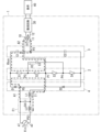
- FIG. 1 is a schematic circuit diagram of an isolated AC/DC converter according to an embodiment of the present disclosure.
- FIG. 2 is a waveform diagram of a current flowing through an inductor provided in the isolated AC/DC converter and a voltage generated in a primary winding of a transformer.
- FIG. 3 is a schematic circuit diagram illustrating a current path in the first operation mode in the isolated AC/DC converter.
- FIG. 4 is a schematic circuit diagram illustrating a current path in the above-mentioned isolated AC/DC converter in a second operation mode.
- FIG. 5 is a schematic circuit diagram illustrating a current path in the above-mentioned isolated AC/DC converter in a third operation mode.
- FIG. 6 is a schematic circuit diagram illustrating a current path in a fourth operation mode in the isolated AC/DC converter.
- an isolated AC/DC converter 1 of this embodiment includes a first rectifier circuit 4, a first series circuit 2, a second series circuit 3, a third capacitor C3, an inductor L1, a transformer 10, a second rectifier circuit 30, and a control circuit 20.
- the second rectifier circuit 30 is abbreviated as "rectifier circuit.”
- the first rectifier circuit 4 includes a series circuit of a first diode D1 and a second diode D2 whose cathode is connected to the anode of the first diode D1.
- the first end a1 of the AC power supply PS1 is connected to a connection point P5 between the first diode D1 and the second diode D2.
- the first series circuit 2 includes a first semiconductor switch S1, a second semiconductor switch S2, a third semiconductor switch S3, and a fourth semiconductor switch S4 connected in series between the cathode of the first diode D1 and the anode of the second diode D2.
- the second end a2 of the AC power supply PS1 is connected to a connection point P1 between the second semiconductor switch S2 and the third semiconductor switch S3.
- the second series circuit 3 includes a series circuit of a first capacitor C1 and a second capacitor C2, and is connected in parallel with the first series circuit 2.
- the third capacitor C3 is connected between the connection point P3 of the first semiconductor switch S1 and the second semiconductor switch S2 and the connection point P4 of the third semiconductor switch S3 and the fourth semiconductor switch S4.
- the inductor L1 is connected between at least one of the first rectifier circuit 4 and the first series circuit 2 and the AC power supply PS1. In the circuit shown in FIG. 1, the inductor L1 is connected between the first series circuit 2 and the AC power supply PS1.
- the transformer 10 has a primary winding 11 connected between a connection point P1 between the second semiconductor switch S2 and the third semiconductor switch S3 and a connection point P2 between the first capacitor C1 and the second capacitor C2.
- the second rectifier circuit 30 is connected to the secondary winding 12 of the transformer 10, rectifies the current flowing through the secondary winding 12, and outputs it to the load 40.
- the control circuit 20 controls each of the first semiconductor switch S1, the second semiconductor switch S2, the third semiconductor switch S3, and the fourth semiconductor switch S4 to an on or off state.
- two circuit elements being connected refers to a state in which the two circuit elements are electrically connected, and is not limited to a state in which the two circuit elements are directly connected, but may include a state in which the two circuit elements are indirectly connected via another circuit element.
- the isolated AC/DC converter 1 may be abbreviated to converter 1
- the first to fourth semiconductor switches S1 to S4 may be abbreviated to first to fourth switches S1 to S4, respectively.
- connection point P1 may be abbreviated to the first connection point
- connection point P2 may be abbreviated to the second connection point.
- the control circuit 20 controls each of the first to fourth switches S1 to S4 to an on or off state, thereby controlling the charging voltage of each of the first to third capacitors C1 to C3. Since a voltage higher than the charging voltage of the first capacitor C1 and the second capacitor C2 is not applied to the first to fourth switches S1 to S4, by controlling the charging voltage of the first capacitor C1 and the second capacitor C2, the voltage applied to the first to fourth switches S1 to S4 can be suppressed, and semiconductor switches with low voltage resistance can be used for the first to fourth switches S1 to S4.
- a current flows through the primary winding 11 of the transformer 10 and power is supplied to the load 40 connected to the secondary winding 12 of the transformer 10 in an operation mode (first operation mode described later) in which the first switch S1 and the second switch S2 are on and the third switch S3 and the fourth switch S4 are off, and an operation mode (fourth operation mode described later) in which the third switch S3 and the fourth switch S4 are on and the first switch S1 and the second switch S2 are off. Therefore, the control circuit 20 can adjust the proportion of the first operation mode and the fourth operation mode within one switching period in which the first to fourth switches S1 to S4 are switched, thereby adjusting the power supplied to the load 40.
- control circuit 20 can adjust the power supplied to load 40 without changing the switching periods of first to fourth switches S1 to S4.
- FIG. 1 is a schematic circuit diagram of a converter 1.
- Converter 1 is an isolated AC/DC converter that converts AC voltage input from an AC power source PS1, such as a commercial AC power source, into DC voltage and supplies it to a load 40.
- an AC power source PS1 such as a commercial AC power source
- the converter 1 includes the first rectifier circuit 4, the first series circuit 2, the second series circuit 3, the third capacitor C3, the inductor L1, the transformer 10, the second rectifier circuit 30, and the control circuit 20.
- the converter 1 also includes a filter circuit F1. Note that the first rectifier circuit 4, the third capacitor C3, and the transformer 10 are as described in "(1) Overview,” and therefore will not be described here.
- the first series circuit 2 includes the first to fourth switches S1 to S4 connected in series between the cathode of the first diode D1 and the anode of the second diode D2.
- the first to fourth switches S1 to S4 are connected between the cathode of the first diode D1 and the anode of the second diode D2 in the order of the first switch S1, the second switch S2, the third switch S3, and the fourth switch S4.
- the first to fourth switches S1 to S4 are, for example, N-channel MOSFETs (Metal-Oxide-Semiconductor Field Effect Transistors).
- Each of the first to fourth switches S1 to S4 is controlled to an on or off state by a control signal input from the control circuit 20 to its gate electrode.
- the second series circuit 3 has a series circuit of a first capacitor C1 and a second capacitor C2, and is connected in parallel with the first series circuit 2.
- the capacitance of the first capacitor C1 and the capacitance of the second capacitor C2 are the same value.
- the circuit constants (e.g., capacitance) of the two circuit elements being the same does not necessarily mean that the circuit constants of the two circuit elements are completely identical, but may also include cases where the difference in the circuit constants of the two circuit elements is small enough to be considered a manufacturing error.
- the voltage of the connection point P2 between the first capacitor C1 and the second capacitor C2 is half the voltage Vbus between both ends of the second series circuit 3.
- the control circuit 20 is primarily configured, for example, as a computer system having one or more processors and memory.
- the functions of the control circuit 20 are realized by the processor of the computer system executing a program recorded in the memory of the computer system.
- the program may be recorded in the memory, or may be provided via a telecommunications line such as the Internet, or may be recorded on a non-transitory recording medium such as a memory card and provided.
- the control circuit 20 receives, for example, the voltage Vbus across the second series circuit 3 including the series circuit of the first capacitor C1 and the second capacitor C2, the charging voltage V3 of the third capacitor C3, and the voltage V1 across the primary winding 11 of the transformer 10 as feedback.
- the control circuit 20 controls the power supplied to the load 40 by controlling each of the first to fourth switches S1 to S4 to an on or off state based on the feedback values of the voltage Vbus, the charging voltage V3, and the voltage V1.
- the filter circuit F1 is an LC filter including a coil L2 whose first end is connected to the second end a2 of the AC power supply PS1, and a capacitor C4 connected between the first end a1 of the AC power supply PS1 and the second end of the coil L2.
- the inductor L1 is connected between the connection point P1 of the second switch S2 and the third switch S3 and the second end a2 of the AC power supply PS1. More specifically, the inductor L1 is connected between the connection point P1 of the second switch S2 and the third switch S3 and the coil L2.
- the pair of input terminals of the second rectifier circuit 30 are connected to both ends of the secondary winding 12 of the transformer 10.
- the second rectifier circuit 30 includes, for example, a diode bridge circuit in which a plurality of diodes are bridge-connected.
- the pair of input terminals of the diode bridge circuit are connected to the secondary winding 12 of the transformer 10.
- the converter 1 further includes, in the stage subsequent to the second rectifier circuit 30, a smoothing circuit that smoothes the pulsating voltage output from the second rectifier circuit 30.
- the DC voltage rectified by the second rectifier circuit 30 and smoothed by the smoothing circuit is supplied to the load 40.
- the control circuit 20 controls each of the first to fourth switches S1 to S4 to an on or off state by outputting a control signal to the gate electrodes of the first to fourth switches S1 to S4.
- the operation modes of the first to fourth switches S1 to S4 include a first operation mode, a second operation mode, a third operation mode, and a fourth operation mode.
- the first operation mode the first switch S1 and the second switch S2 are in an on state, and the third switch S3 and the fourth switch S4 are in an off state.
- the second operation mode the first switch S1 and the third switch S3 are in an on state, and the second switch S2 and the fourth switch S4 are in an off state.
- the second switch S2 and the fourth switch S4 are in an on state, and the first switch S1 and the third switch S3 are in an off state.
- the third switch S3 and the fourth switch S4 are in an on state, and the first switch S1 and the second switch S2 are in an off state.
- the control circuit 20 controls the operation mode to periodically repeat a first period t1 in which the operation mode is the first operation mode, a second period t2 in which the operation mode is the second operation mode or the third operation mode, a third period t3 in which the operation mode is the fourth operation mode, and a fourth period t4 in which the operation mode is the second operation mode or the third operation mode.
- the control circuit 20 controls the time lengths of the first period t1, the second period t2, the third period t3, and the fourth period t4 so that the inductor L1 operates in a discontinuous mode in which the current I1 flowing through the inductor L1 is discontinuous. Specifically, the control circuit 20 controls the time lengths of the first period t1 and the third period to be the same. The control circuit 20 controls the time lengths of the first period t1, the second period t2, the third period t3, and the fourth period t4 so that the voltage Vbus between both ends of the second series circuit 3 is at least twice the peak value of the input voltage Vin input from the AC power supply PS1.
- time lengths of the two operation modes being the same are not limited to the time lengths of the two operation modes being completely the same, and may include a state in which the difference in time length between the two operation modes is within ⁇ a few percent (e.g. ⁇ 10%) of either time length.
- Figs. 2 to 6 explain the current path when the input voltage Vin from AC power supply PS1 is in a positive half cycle in which the first terminal a1 has a higher potential than the second terminal a2.
- FIG. 2 is a waveform diagram of the current I1 flowing through the inductor L1 and the voltage V1 generated in the primary winding 11 of the transformer 10.
- periods t1 to t4 correspond to the first to fourth periods, respectively.
- period T1 indicates the period of one switching cycle of the first to fourth switches S1 to S4, and the switching frequency of the first to fourth switches S1 to S4 is, for example, about 100 kHz.
- FIG. 2 shows the waveform diagram of the current I1 and voltage V1 for one switching cycle.
- FIGS. 3 to 6 are schematic circuit diagrams showing paths through which current flows in the first, second, third, and fourth operating modes, respectively.
- the on/off states of the first to fourth switches S1 to S4 are shown diagrammatically, and the control circuit 20 is omitted.
- the dotted arrows A1 to A6 in FIG. 3 to FIG. 6 indicate paths through which current flows. Note that the following describes the current paths when the input voltage Vin from the AC power supply PS1 is in a positive half cycle in which the first terminal a1 is at a higher potential than the second terminal a2.
- the control circuit 20 controls the first switch S1 and the second switch S2 to an on state, and controls the third switch S3 and the fourth switch S4 to an off state.
- the voltage at the connection point P1 between the second switch S2 and the third switch S3 becomes equal to the voltage Vbus.
- a current flows from the AC power supply PS1 to the first diode D1 to the first switch S1 to the second switch S2 to the inductor L1 to the coil L2 to the AC power supply PS1 (the path indicated by the arrow A1).
- the first capacitor C1 is connected in parallel with the primary winding 11 of the transformer 10, so that the voltage V1 across the primary winding 11 of the transformer 10 is equal to the charging voltage (Vbus/2) of the first capacitor C1 (see FIG. 2).
- a current flows from the first capacitor C1 to the first switch S1 to the second switch S2 to the primary winding 11 to the first capacitor C1 (the path indicated by the arrow A2).
- a second rectifier circuit 30 is connected to the secondary winding 12 of the transformer 10, and the current generated in the secondary winding 12 of the transformer 10 is rectified by the second rectifier circuit 30 and smoothed by the smoothing circuit to generate a DC voltage of a predetermined voltage value, and DC power is supplied to the load 40.
- the control circuit 20 switches the operation mode of the converter 1 from the first operation mode to the second operation mode or the third operation mode.
- the control circuit 20 controls the operation mode in the second period t2 to either the second operation mode or the third operation mode depending on the charging voltage V3 of the third capacitor C3.
- the control circuit 20 controls the operation mode in the second period to the second operation mode.
- the threshold voltage Vth is set to half the voltage Vbus.
- the control circuit 20 controls the operation mode in the second period to the third operation mode.
- FIG. 4 is a schematic circuit diagram showing the current path when operating in the second operating mode.
- the control circuit 20 controls the first switch S1 and the third switch S3 to the on state, and controls the second switch S2 and the fourth switch S4 to the off state.
- the voltage of the connection point P1 of the second switch S2 and the third switch S3 becomes equal to the voltage (Vbus/2) of the connection point P2 of the first capacitor C1 and the second capacitor C2.
- a current flows from the AC power supply PS1 to the first diode D1, the first switch S1, the third capacitor C3, the third switch S3, the inductor L1, the coil L2, and the AC power supply PS1 (the path indicated by the arrow A3).
- the inductor L1 releases the energy stored in the first operating mode and charges the third capacitor C3.
- the voltage applied to the inductor L1 is (Vin-Vbus/2), and since the voltage Vbus is charged to a voltage greater than twice the maximum value of the input voltage Vin, (Vin-Vbus/2) ⁇ 0. Therefore, the current I1 flowing through the inductor L1 gradually decreases at a rate of (Vin-Vbus/2)/L.
- no current flows through the primary winding 11 of the transformer 10, and no power is supplied to the secondary side of the transformer 10.
- FIG. 5 is a schematic circuit diagram showing the current path when operating in the third operating mode.
- the control circuit 20 controls the operating mode to the third operating mode in the second period, the control circuit 20 controls the second switch S2 and the fourth switch S4 to the on state, and controls the first switch S1 and the third switch S3 to the off state.
- the voltage of the connection point P1 of the second switch S2 and the third switch S3 is equal to the voltage (Vbus/2) of the connection point P2 of the first capacitor C1 and the second capacitor C2.
- the third operating mode while the energy stored in inductor L1 remains, a current flows from AC power supply PS1 to first diode D1 to first capacitor C1 to second capacitor C2 to fourth switch S4 to third capacitor C3 to second switch S2 to inductor L1 to coil L2 to AC power supply PS1 (path indicated by arrow A4). At this time, the third capacitor C3 is discharged and the first capacitor C1 and second capacitor C2 are charged.
- the voltage applied to inductor L1 is (Vin-Vbus/2), and since the voltage Vbus is charged to a voltage greater than twice the maximum value of the input voltage Vin, (Vin-Vbus/2) ⁇ 0.
- the current I1 flowing through inductor L1 gradually decreases at a rate of (Vin-Vbus/2)/L.
- no current flows through the primary winding 11 of the transformer 10, and no power is supplied to the secondary side of the transformer 10.
- the control circuit 20 controls the operation mode of the converter 1 to the fourth operation mode during the third period t3.
- the control circuit 20 controls the third switch S3 and the fourth switch S4 to the on state, and controls the first switch S1 and the second switch S2 to the off state.
- the voltage at the connection point P1 between the second switch S2 and the third switch S3 becomes 0.
- a current flows through the path AC power supply PS1 ⁇ first diode D1 ⁇ first capacitor C1 ⁇ second capacitor C2 ⁇ fourth switch S4 ⁇ third switch S3 ⁇ inductor L1 ⁇ coil L2 ⁇ AC power supply PS1 (path indicated by arrow A5), charging the first capacitor C1 and the second capacitor C2.
- the second capacitor C2 is connected in parallel with the primary winding 11 of the transformer 10, and the voltage V1 across the primary winding 11 of the transformer 10 is equal to (-Vbus/2) (see FIG. 2).
- a current flows through the path (path indicated by arrow A6) of the second capacitor C2 ⁇ primary winding 11 ⁇ third switch S3 ⁇ fourth switch S4 ⁇ second capacitor C2, and power is supplied to the secondary side of the transformer 10.
- the voltage applied to inductor L1 is (Vin - Vbus), and since the voltage Vbus is charged to a voltage greater than twice the maximum value of the input voltage Vin, (Vin - Vbus) ⁇ 0. Therefore, the current I1 flowing through inductor L1 gradually decreases at a slope of (Vin - Vbus)/L1 (see Figure 2). Since the control circuit 20 controls the duration of the first period t1 and the duration of the third period t3 to be the same length, in the third period, the voltage Vbus is charged to more than twice the peak value of the input voltage Vin, and the current I1 becomes zero. Then, the current I1 does not flow until it switches back to the first operating mode.
- the control circuit 20 controls the operation mode of the converter 1 to the second operation mode or the third operation mode in the fourth period t4.
- the control circuit 20 controls the operation mode in the fourth period t4 to either the second operation mode or the third operation mode.
- the fourth period t4 no current flows through the inductor L1, and no power is transferred from the primary side to the secondary side of the transformer 10, so the operation mode in the fourth period t4 may be either the second operation mode or the third operation mode.
- the voltage Vbus is charged to more than twice the peak value of the input voltage Vin, and the third capacitor C3 is also charged to the threshold voltage, so that no current I1 flows through the inductor L1 in the fourth period t4.
- no current flows through the primary winding 11 of the transformer 10, and no power is supplied to the secondary side of the transformer 10.
- a fourth period in which the control circuit 20 operates in the second operation mode or the third operation mode is provided between the third period in which the control circuit 20 operates in the fourth operation mode and the first period in which the control circuit 20 operates in the fourth operation mode.
- the control circuit 20 switches the operation mode of the converter 1 from the fourth operation mode to the first operation mode.
- the operation of the first operation mode is as described above.
- the first switch S1 can be switched from the off state to the on state while the current I1 is zero. This reduces the possibility of an inrush current flowing when the first switch S1 is switched from the off state to the on state.
- the fourth period t4 is not essential and may be omitted.
- the control circuit 20 controls the first to fourth switches S1 to S4 so that the first period t1, the second period t2, the third period t3, and the fourth period t4 are repeated periodically in this order, and the voltage Vbus between both ends of the second series circuit 3 and the voltage V1 applied to the primary winding 11 of the transformer 10 can be controlled.
- the converter 1 of this embodiment is a multilevel converter circuit in which the voltage at the connection point between the second switch S2 and the third switch S3 changes to three levels: Vbus, (Vbus/2), and 0.
- the control circuit 20 controls the time lengths of the first period t1, the second period t2, and the third period t3 so that the time lengths of the first period t1 and the third period t3 are the same, and the voltage Vbus between both ends of the second series circuit 3 is at least twice the peak value of the input voltage Vin input from the AC power supply PS1.
- the current I1 becomes zero in the middle of the third period t3, and switching operation can be performed in a discontinuous mode in which the current I1 becomes discontinuous.
- the current I1 flows in a manner roughly proportional to the input voltage Vin from the AC power supply PS1, which has the advantage of improving the power factor.
- the control circuit 20 controls the first to fourth switches S1 to S4 to periodically repeat the first period t1, the second period t2, the third period t3, and the fourth period t4 in this order.
- energy is stored in the inductor L1 during the third period t3 in the fourth operation mode, and the energy stored in the inductor L1 is released during the fourth period t4 and the first period t1 after the third period t3.
- the third capacitor C3 is charged in the third operation mode, and discharged in the second operation mode.
- the converter 1 supplies power to the secondary side of the transformer 10 during the first period t1 and the third period t3, and stops the power supply to the secondary side of the transformer 10 during the second period t2 and the fourth period t4.
- the control circuit 20 controls the power supply to the load 40 by making the duration of the first period t1 and the duration of the third period t3 the same, and adjusting the ratio between the total duration of the first period t1 and the third period t3 and the total duration of the second period t2 and the fourth period t4. The greater the ratio of the duration of the first period t1 and the duration of the third period t3 in one cycle T1 of the switching period, the more the power supplied to the load 40 increases.
- control circuit 20 can adjust the period during which power is supplied to the secondary side of the transformer 10 by adjusting the ratio between the total duration of the first period t1 and the third period t3 and the total duration of the second period t2 and the fourth period t4. Therefore, the control circuit 20 can adjust the power supplied to the load 40 without changing the switching frequencies of the first to fourth switches S1 to S4.
- the converter 1 in the present disclosure includes a computer system.
- the computer system is mainly composed of a processor and a memory as hardware.
- the function of the converter 1 in the present disclosure as the control circuit 20 is realized by the processor executing a program recorded in the memory of the computer system.
- the program may be pre-recorded in the memory of the computer system, may be provided through a telecommunications line, or may be recorded and provided on a non-transitory recording medium such as a memory card, an optical disk, or a hard disk drive that can be read by the computer system.
- the processor of the computer system is composed of one or more electronic circuits including a semiconductor integrated circuit (IC) or a large scale integrated circuit (LSI).
- IC semiconductor integrated circuit
- LSI large scale integrated circuit
- the integrated circuits such as ICs or LSIs referred to here are called different names depending on the degree of integration, and include integrated circuits called system LSIs, VLSIs (Very Large Scale Integration), or ULSIs (Ultra Large Scale Integration).
- a field-programmable gate array (FPGA) that is programmed after the LSI is manufactured, or a logic device that allows the reconfiguration of the connection relationships within the LSI or the reconfiguration of the circuit partitions within the LSI, can also be used as a processor.
- FPGA field-programmable gate array
- Multiple electronic circuits may be integrated into one chip, or may be distributed across multiple chips. Multiple chips may be integrated into one device, or may be distributed across multiple devices.
- the computer system referred to here includes a microcontroller having one or more processors and one or more memories.
- the microcontroller is also composed of one or more electronic circuits including a semiconductor integrated circuit or a large-scale integrated circuit.
- control circuit 20 controls the first to fourth switches S1 to S4 to the on or off state so that the first period t1, the second period t2, the third period t3, and the fourth period t4 are repeated in this order, but the second period t2 and the fourth period t4 are not essential and can be omitted.
- the control circuit 20 may set the fourth period t4 to zero and perform control so that the first period t1, the second period t2, and the third period t3 are repeated periodically, thereby shortening the switching period.
- the control circuit 20 can omit the second period t2 because no current flows through the inductor L1 during the second period t2 and no energy is transferred to the secondary side of the transformer 10. Therefore, the control circuit 20 may set the second period t2 to zero and perform control so that the first period t1, the third period t3, and the fourth period t4 are repeated periodically, thereby shortening the switching period.
- the first to fourth semiconductor switches S1 to S4 are N-channel MOSFETs, but the first to fourth semiconductor switches S1 to S4 may be semiconductor switches such as bipolar transistors or IGBTs (Insulated Gate Bipolar Transistors).
- the inductor L1 is connected between the first series circuit 2 and the AC power supply PS1, but the inductor L1 may be connected between the first rectifier circuit 4 and the AC power supply PS1, that is, between the connection point P5 of the first diode D1 and the second diode D2 and the first end a1 of the AC power supply PS1.
- the inductor L1 may be connected between the first series circuit 2 and the AC power supply PS1, and between the first rectifier circuit 4 and the AC power supply PS1.
- the converter 1 includes a filter circuit F1 such as an LC filter, but the circuit configuration of the filter circuit F1 can be changed as appropriate. Also, the filter circuit F1 is not an essential component of the converter 1, and can be omitted as appropriate.
- the second rectifier circuit 30 including a diode bridge circuit is connected to the secondary side of the transformer 10, but the configuration of the second rectifier circuit 30 can be changed as appropriate, and may be a full-bridge type converter circuit, etc.
- the isolated AC/DC converter (1) of the first aspect includes a first rectifier circuit (4), a first series circuit (2), a second series circuit (3), a third capacitor (C3), an inductor (L1), a transformer (10), a second rectifier circuit (30), and a control circuit (20).
- the first rectifier circuit (4) includes a series circuit of a first diode (D1) and a second diode (D2) having a cathode connected to the anode of the first diode (D1), and a first end (a1) of an AC power supply (PS1) is connected to the connection point of the first diode (D1) and the second diode (D2).
- the first series circuit (2) includes a first semiconductor switch (S1), a second semiconductor switch (S2), a third semiconductor switch (S3), and a fourth semiconductor switch (S4) connected in series between the cathode of the first diode (D1) and the anode of the second diode (D2), and a second end (a2) of the AC power supply (PS1) is connected to a connection point between the second semiconductor switch (S2) and the third semiconductor switch (S3).
- the second series circuit (3) includes a series circuit of a first capacitor (C1) and a second capacitor (C2), and is connected in parallel with the first series circuit (2).
- the third capacitor (C3) is connected between the connection point of the first semiconductor switch (S1) and the second semiconductor switch (S2) and the connection point of the third semiconductor switch (S3) and the fourth semiconductor switch (S4).
- the inductor (L1) is connected between at least one of the first rectifier circuit (4) and the first series circuit (2) and the AC power supply (PS1).
- the transformer (10) has a primary winding (11) connected between the connection point of the second semiconductor switch (S2) and the third semiconductor switch (S3) and the connection point of the first capacitor (C1) and the second capacitor (C2).
- the second rectifier circuit (30) is connected to the secondary winding (12) of the transformer (10) and rectifies the current flowing through the secondary winding (12) and outputs it to the load (40).
- the control circuit (20) controls each of the first semiconductor switch (S1), the second semiconductor switch (S2), the third semiconductor switch (S3), and the fourth semiconductor switch (S4) to an on state or an off state.
- a current flows through the primary winding (11) of the transformer (10), and power is supplied to the load (40) connected to the secondary winding (12) of the transformer (10).
- a current flows through the primary winding (11) of the transformer (10), and power is supplied to the load (40) connected to the secondary winding (12) of the transformer (10).
- control circuit (20) can adjust the ratio of the first operation mode and the fourth operation mode within one switching period in which the first to fourth semiconductor switches (S1 to S4) are switched, thereby adjusting the power supplied to the load (40). Furthermore, since a current roughly proportional to the input voltage from the AC power supply (PS1) flows through the inductor (L1), an isolated AC/DC converter (1) capable of improving the power factor can be realized with simple control.
- the capacitance of the first capacitor (C1) is the same as the capacitance of the second capacitor (C2).
- the voltage at the connection point between the first capacitor (C1) and the second capacitor (C2) can be set to half the voltage (Vbus) between both ends of the second series circuit (3).
- the operation modes of the first to fourth semiconductor switches (S1 to S4) include a first operation mode, a second operation mode, a third operation mode, and a fourth operation mode.
- the first operation mode the first semiconductor switch (S1) and the second semiconductor switch (S2) are in an on state, and the third semiconductor switch (S3) and the fourth semiconductor switch (S4) are in an off state.
- the second operation mode the first semiconductor switch (S1) and the third semiconductor switch (S3) are in an on state, and the second semiconductor switch (S2) and the fourth semiconductor switch (S4) are in an off state.
- the second semiconductor switch (S2) and the fourth semiconductor switch (S4) are in an on state, and the first semiconductor switch (S1) and the third semiconductor switch (S3) are in an off state.
- the fourth operation mode the third semiconductor switch (S3) and the fourth semiconductor switch (S4) are in an ON state, and the first semiconductor switch (S1) and the second semiconductor switch (S2) are in an OFF state.
- the control circuit (20) controls so as to periodically repeat a first period in which the operation mode is the first operation mode, a second period in which the operation mode is the second operation mode or the fourth operation mode, a third period in which the operation mode is the third operation mode, and a fourth period in which the operation mode is the second operation mode or the third operation mode.
- control circuit (20) controls the operation mode to either the second operation mode or the fourth operation mode in accordance with the charging voltage of the third capacitor (C3) during each of the second and fourth periods.
- control circuit (20) can control the operation mode during each of the second and fourth periods to either a second operation mode in which the third capacitor (C3) is charged or a third operation mode in which the third capacitor (C3) is discharged, depending on the charging voltage of the third capacitor (C3).
- control circuit (20) controls the time lengths of the first, second, third, and fourth periods so as to operate in a discontinuous mode in which the current flowing through the inductor (L1) is discontinuous.
- This method makes it possible to suppress the inrush current that occurs during switching.
- control circuit (20) controls the time length of the first period to be the same as the time length of the third period, and controls the time lengths of the first period, second period, third period, and fourth period so that the voltage between both ends of the second series circuit (3) is at least twice the peak value of the input voltage input from the AC power supply (PS1).
- the control circuit (20) controls the converter so that in a positive half cycle in which the first terminal (a1) of the AC power supply (PS1) is at a higher potential than the second terminal (a2), the fourth period is set to zero, and the first period, the second period, and the third period are periodically repeated.
- the control circuit (20) controls the converter so that the second period is set to zero, and the first period, the third period, and the fourth period are periodically repeated.
- control circuit (20) controls the duration of the first period and the duration of the third period to be the same duration.
- the control circuit (20) controls the power supplied to the load (40) by adjusting the ratio between the total duration of the first period and the third period and the total duration of the second period and the fourth period.
- the control circuit (20) can control the power supply to the load (40) by adjusting the ratio between the total time length of the first and third periods during which the control circuit (20) operates in the first and fourth operating modes, respectively, and the total time length of the second and fourth periods during which the control circuit (20) operates in the second or third operating mode.
- the second rectifier circuit (30) includes a diode bridge circuit.
- the second rectifier circuit (30) is configured as a diode bridge circuit that does not require control, so the configuration of the control circuit (20) can be simplified.
- the configurations according to the second to ninth aspects are not essential for the isolated AC/DC converter (1) and may be omitted as appropriate.
Landscapes
- Engineering & Computer Science (AREA)
- Power Engineering (AREA)
- Dc-Dc Converters (AREA)
Priority Applications (2)
| Application Number | Priority Date | Filing Date | Title |
|---|---|---|---|
| CN202480046552.8A CN121488397A (zh) | 2023-07-28 | 2024-06-28 | 隔离式ac/dc转换器 |
| JP2025537751A JPWO2025028110A1 (https=) | 2023-07-28 | 2024-06-28 |
Applications Claiming Priority (2)
| Application Number | Priority Date | Filing Date | Title |
|---|---|---|---|
| JP2023-123804 | 2023-07-28 | ||
| JP2023123804 | 2023-07-28 |
Publications (1)
| Publication Number | Publication Date |
|---|---|
| WO2025028110A1 true WO2025028110A1 (ja) | 2025-02-06 |
Family
ID=94394403
Family Applications (1)
| Application Number | Title | Priority Date | Filing Date |
|---|---|---|---|
| PCT/JP2024/023674 Pending WO2025028110A1 (ja) | 2023-07-28 | 2024-06-28 | 絶縁型ac/dcコンバータ |
Country Status (3)
| Country | Link |
|---|---|
| JP (1) | JPWO2025028110A1 (https=) |
| CN (1) | CN121488397A (https=) |
| WO (1) | WO2025028110A1 (https=) |
Citations (4)
| Publication number | Priority date | Publication date | Assignee | Title |
|---|---|---|---|---|
| JP2015027169A (ja) * | 2013-07-26 | 2015-02-05 | 新電元工業株式会社 | 絶縁型マルチレベルコンバータ |
| WO2016031061A1 (ja) * | 2014-08-29 | 2016-03-03 | 新電元工業株式会社 | 力率改善コンバータ、及び、力率改善コンバータを備えた電源装置 |
| JP2019097300A (ja) * | 2017-11-22 | 2019-06-20 | 富士電機株式会社 | 3レベル電力変換装置 |
| WO2022023527A1 (en) * | 2020-07-30 | 2022-02-03 | Prodrive Technologies Innovation Services B.V. | Multi-level bidirectional electrical ac/dc converter |
-
2024
- 2024-06-28 WO PCT/JP2024/023674 patent/WO2025028110A1/ja active Pending
- 2024-06-28 JP JP2025537751A patent/JPWO2025028110A1/ja active Pending
- 2024-06-28 CN CN202480046552.8A patent/CN121488397A/zh active Pending
Patent Citations (4)
| Publication number | Priority date | Publication date | Assignee | Title |
|---|---|---|---|---|
| JP2015027169A (ja) * | 2013-07-26 | 2015-02-05 | 新電元工業株式会社 | 絶縁型マルチレベルコンバータ |
| WO2016031061A1 (ja) * | 2014-08-29 | 2016-03-03 | 新電元工業株式会社 | 力率改善コンバータ、及び、力率改善コンバータを備えた電源装置 |
| JP2019097300A (ja) * | 2017-11-22 | 2019-06-20 | 富士電機株式会社 | 3レベル電力変換装置 |
| WO2022023527A1 (en) * | 2020-07-30 | 2022-02-03 | Prodrive Technologies Innovation Services B.V. | Multi-level bidirectional electrical ac/dc converter |
Also Published As
| Publication number | Publication date |
|---|---|
| CN121488397A (zh) | 2026-02-06 |
| JPWO2025028110A1 (https=) | 2025-02-06 |
Similar Documents
| Publication | Publication Date | Title |
|---|---|---|
| US8837174B2 (en) | Switching power-supply apparatus including switching elements having a low threshold voltage | |
| JP3861220B2 (ja) | Dc−dcコンバータ | |
| KR20040020862A (ko) | 탭핑된-인덕터 점감 변환기 | |
| TWI849969B (zh) | 轉換裝置 | |
| JP2010516223A (ja) | スナバを有する電力コンバータ | |
| JP2018098998A (ja) | 絶縁同期整流型dc/dcコンバータ、同期整流コントローラ、電源アダプタおよび電子機器 | |
| JP2011526478A (ja) | 共振型電力コンバータ | |
| CN102239628A (zh) | 用于减少来自环振荡的emi的切换功率转换器及其控制方法 | |
| US11973440B2 (en) | Isolated DC/DC converter with secondary-side full bridge diode rectifier and asymmetrical auxiliary capacitor | |
| JP4166219B2 (ja) | 複共振dc−dcコンバータ | |
| TW202107809A (zh) | 切換式電力轉換器、及一次側控制器及其控制方法 | |
| US7688044B2 (en) | Device for transforming and stabilizing a primary AC voltage for supplying an electric load | |
| US20060279968A1 (en) | DC/AC converter circuit and DC/AC conversion method | |
| WO2025028110A1 (ja) | 絶縁型ac/dcコンバータ | |
| WO2025028108A1 (ja) | 絶縁型ac/dcコンバータ | |
| JP3354454B2 (ja) | スイッチング電源装置 | |
| WO2023127464A1 (ja) | 電力変換システム | |
| JP7543296B2 (ja) | スイッチング制御回路及びスイッチング電源装置 | |
| JPH01218352A (ja) | スイッチング電源回路 | |
| TW202406291A (zh) | 高效率之電源供應器 | |
| CN211670785U (zh) | Llc谐振电路的控制装置及直流-直流转换器 | |
| KR102076577B1 (ko) | 양방향 직류-직류 컨버터 | |
| CN113014101A (zh) | Llc谐振电路的控制装置和方法及直流-直流转换器 | |
| TWI831624B (zh) | 電力轉換系統 | |
| JP3235711B2 (ja) | スイッチング電源 |
Legal Events
| Date | Code | Title | Description |
|---|---|---|---|
| 121 | Ep: the epo has been informed by wipo that ep was designated in this application |
Ref document number: 24848769 Country of ref document: EP Kind code of ref document: A1 |
|
| WWE | Wipo information: entry into national phase |
Ref document number: 2501008659 Country of ref document: TH |
|
| ENP | Entry into the national phase |
Ref document number: 2025537751 Country of ref document: JP Kind code of ref document: A |
|
| WWE | Wipo information: entry into national phase |
Ref document number: 2025537751 Country of ref document: JP |
|
| NENP | Non-entry into the national phase |
Ref country code: DE |