WO2025027977A1 - 電界効果トランジスタ - Google Patents
電界効果トランジスタ Download PDFInfo
- Publication number
- WO2025027977A1 WO2025027977A1 PCT/JP2024/018533 JP2024018533W WO2025027977A1 WO 2025027977 A1 WO2025027977 A1 WO 2025027977A1 JP 2024018533 W JP2024018533 W JP 2024018533W WO 2025027977 A1 WO2025027977 A1 WO 2025027977A1
- Authority
- WO
- WIPO (PCT)
- Prior art keywords
- layer
- contact
- layers
- semiconductor substrate
- inter
- Prior art date
- Legal status (The legal status is an assumption and is not a legal conclusion. Google has not performed a legal analysis and makes no representation as to the accuracy of the status listed.)
- Pending
Links
Images




Classifications
-
- H—ELECTRICITY
- H10—SEMICONDUCTOR DEVICES; ELECTRIC SOLID-STATE DEVICES NOT OTHERWISE PROVIDED FOR
- H10D—INORGANIC ELECTRIC SEMICONDUCTOR DEVICES
- H10D30/00—Field-effect transistors [FET]
- H10D30/60—Insulated-gate field-effect transistors [IGFET]
- H10D30/64—Double-diffused metal-oxide semiconductor [DMOS] FETs
- H10D30/66—Vertical DMOS [VDMOS] FETs
Definitions
- the technology disclosed in this specification relates to field effect transistors.
- the field effect transistor disclosed in JP 2001-267570 A has a trench-type gate electrode.
- This field effect transistor also has a p-type deep layer (also called the electric field shield region below the base region) that extends downward from a p-type body layer (also called the base region).
- the deep layer extends to a position lower than the bottom end of the trench.
- a p-type contact layer that connects the body layer and the source electrode is provided on top of the deep layer. The contact layer is provided to stabilize the potential of the body layer.
- the deep layer is provided to reduce the electric field strength of the gate insulating film in the trench.
- the field effect transistor disclosed in this specification includes a semiconductor substrate made of a compound semiconductor and having a plurality of trenches on its upper surface, a plurality of gate electrodes each disposed in a corresponding one of the trenches and insulated from the semiconductor substrate by a gate insulating film, and a source electrode in contact with the upper surface of the semiconductor substrate.
- the semiconductor substrate includes a plurality of n-type source layers, a plurality of p-type contact layers, a p-type body layer, an n-type drift layer, and a plurality of p-type deep layers.
- Each semiconductor region located between the plurality of trenches in the semiconductor substrate is an inter-trench region.
- Each of the source layers is disposed in the corresponding inter-trench region, is in contact with the source electrode, and is in contact with the corresponding gate insulating film.
- Each of the contact layers is disposed in the corresponding inter-trench region, and is in contact with the source electrode.
- a plurality of the contact layers are provided in each of the inter-trench regions. When the semiconductor substrate is viewed from above, the plurality of contact layers are disposed in each of the inter-trench regions with a gap therebetween in a specific direction parallel to the plurality of trenches.
- the body layer has a lower p-type impurity concentration than each of the contact layers, is distributed across the multiple inter-trench regions, is disposed below each of the source layers and each of the contact layers, and is in contact with the gate insulating film.
- the drift layer is distributed across the lower regions of the multiple inter-trench regions, is in contact with the body layer from below in each of the inter-trench regions, and is in contact with the gate insulating film.
- Each of the deep layers extends from the body layer to a position lower than the lower end of each of the trenches.
- the multiple deep layers are arranged in each of the inter-trench regions with gaps in the specific direction. In each of the inter-trench regions, each of the gaps of the contact layer is disposed above the corresponding deep layer. In each of the inter-trench regions, each of the gaps of the deep layer is disposed below the corresponding contact layer.
- the gap of the contact layer is located above the deep layer, and the gap of the deep layer is located below the contact layer. This reduces the area where the contact layer and deep layer overlap in the vertical direction. As a result, the resistance of the path from the drift layer through the deep layer, body layer, and contact layer to the source electrode (i.e., the path through which the recovery current flows) is high. Therefore, with this field effect transistor, the recovery current can be suppressed.
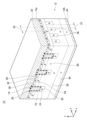
- FIG. 13 is an xz cross-sectional view of a switching element at a position not including a deep layer.
- FIG. 13 is an xz cross-sectional view of a switching element at a position including a deep layer.
- FIG. 13 is a yz cross-sectional view of the switching element at a position that does not include a trench.
- FIG. 2 is a plan view of the upper surface of a semiconductor substrate. 4 is a graph showing impurity concentration distributions in a contact region, a body region, and a source region. 6 is a graph showing the drain current and drain voltage during recovery operation. 13 is a graph showing the relationship between depth D and surge voltage.
- FIG. 6 is a plan view of a switching element according to a first modified example, corresponding to FIG. 5 .
- 13 is a graph showing the relationship between width W and the reduction rate of surge voltage.
- FIG. 7 is a plan view of a switching element according to a second modified example, corresponding to FIG. 5 .
- FIG. 7 is a plan view of a switching element according to a third modified example, the plan view corresponding to FIG. 5 .
- FIG. 10 is a plan view of a switching element according to a fourth modified example, corresponding to FIG. 5 .
- FIG. 13 is a plan view of a switching element according to a fifth modified example, corresponding to FIG. 5 .
- each of the deep layers may intersect with each of the trenches.
- This configuration further reduces the electric field strength of the gate insulating film.
- the contact layers and the deep layers do not need to overlap when the semiconductor substrate is viewed from above.
- the width of the gap in the contact layer can be made wider than the width of the deep layer, and the width of the gap in the deep layer can be made wider than the width of the contact layer.
- This configuration allows recovery current to be suppressed more effectively.
- the gap of the deep layer in each inter-trench region, may have a first gap that overlaps with the contact layer when the semiconductor substrate is viewed from above, and a second gap that does not overlap with the contact layer when the semiconductor substrate is viewed from above.
- the lower end of each of the contact layers may be located at the same position as or higher than the lower end of each of the source layers in the thickness direction of the semiconductor substrate.
- This configuration can suppress depletion of the contact layer, so the recovery current can be suppressed more effectively.
- the MOSFET 10 metal-oxide-semiconductor field effect transistor
- the MOSFET 10 has a semiconductor substrate 12.
- the thickness direction of the semiconductor substrate 12 is referred to as the z-direction
- one direction parallel to the upper surface 12a of the semiconductor substrate 12 is referred to as the x-direction
- the direction perpendicular to the x-direction and z-direction is referred to as the y-direction.
- the semiconductor substrate 12 is made of silicon carbide (i.e., SiC).
- the semiconductor substrate 12 may be made of other compound semiconductors such as gallium nitride and gallium oxide.
- a plurality of trenches 14 are provided on the upper surface 12a of the semiconductor substrate 12. As shown in FIG. 5, the plurality of trenches 14 extend long along the y-direction on the upper surface 12a. The plurality of trenches 14 are arranged at intervals in the x-direction.
- each semiconductor region within the range sandwiched between the trenches 14 is referred to as an inter-trench region 50.
- each trench 14 is covered with a gate insulating film 16.
- a gate electrode 18 is disposed within each trench 14. Each gate electrode 18 is insulated from the semiconductor substrate 12 by the gate insulating film 16. The upper surface of each gate electrode 18 is covered with an interlayer insulating film 20.
- a source electrode 22 is provided on the upper part of the semiconductor substrate 12. The source electrode 22 covers each interlayer insulating film 20. The source electrode 22 is insulated from the gate electrode 18 by the interlayer insulating film 20. The source electrode 22 is in contact with the upper surface 12a of the semiconductor substrate 12 at a position where the interlayer insulating film 20 is not present.
- a drain electrode 24 is disposed on the lower part of the semiconductor substrate 12. The drain electrode 24 is in contact with the entire lower surface 12b of the semiconductor substrate 12.
- the semiconductor substrate 12 has a plurality of source layers 30, a plurality of contact layers 32, a body layer 34, a plurality of deep layers 36, a plurality of trench sublayers 35, a drift layer 38, and a drain layer 40.
- Each contact layer 32 is a p-type layer having a high p-type impurity concentration. As shown in Figures 1, 2, 4, and 5, each contact layer 32 is disposed in an inter-trench region 50. Each contact layer 32 is disposed in a range including the upper surface 12a of the semiconductor substrate 12. A plurality of contact layers 32 are provided in each inter-trench region 50. Each contact layer 32 is disposed in a position that does not contact the trench 14. In each inter-trench region 50, a plurality of contact layers 32 are arranged at intervals along the y direction (i.e., the direction parallel to the trench 14 on the upper surface 12a). In the following, the region between the contact layers 32 in the y direction is referred to as a gap portion 33. Each contact layer 32 is in ohmic contact with the source electrode 22.
- Each source layer 30 is an n-type layer having a high n-type impurity concentration. As shown in FIGS. 1 to 5, each source layer 30 is disposed in the inter-trench region 50. Each source layer 30 is disposed in a range including the upper surface 12a of the semiconductor substrate 12, where the contact layer 32 is not disposed. That is, each source layer 30 is disposed in a region adjacent to the trench 14 and in the gap portion 33. The source layer 30 contacts the side surface of the contact layer 32. Each source layer 30 is in ohmic contact with the source electrode 22. Each source layer 30 contacts the gate insulating film 16 at the top of the side surface of the trench 14. Each source layer 30 faces the gate electrode 18 via the gate insulating film 16.
- the body layer 34 is a p-type layer having a lower p-type impurity concentration than the contact layer 32. As shown in FIGS. 1 to 3, the body layer 34 is distributed across multiple inter-trench regions 50. The body layer 34 is disposed below the multiple source layers 30 and the multiple contact layers 32. The body layer 34 contacts the multiple source layers 30 and the multiple contact layers 32 from below. The body layer 34 contacts the gate insulating film 16 on the side of the trench 14 located below the source layer 30. The body layer 34 faces the gate electrode 18 via the gate insulating film 16.
- each deep layer 36 is a p-type layer protruding downward from the lower surface of the body layer 34.
- Each deep layer 36 extends from the lower surface of the body layer 34 to a position lower than the lower end of each trench 14.
- each deep layer 36 extends long in the x direction and intersects with the trench 14 at an angle of about 90 degrees. That is, each deep layer 36 is distributed across multiple inter-trench regions 50.
- the multiple deep layers 36 are arranged at intervals in the y direction.
- the region between the deep layers 36 in the y direction is referred to as an interval portion 37.
- each deep layer 36 contacts the gate insulating film 16 on the side of the trench 14 located below the body layer 34.
- Each deep layer 36 faces the gate electrode 18 via the gate insulating film 16.
- each trench lower layer 35 is a p-type layer disposed at the bottom of the corresponding trench 14.
- Each trench lower layer 35 extends long along the longitudinal direction (i.e., the y direction) of the corresponding trench 14 and intersects with each deep layer 36.
- Each trench lower layer 35 contacts the gate insulating film 16 at the bottom surface of the corresponding trench 14.
- the drift layer 38 is an n-type layer having a lower n-type impurity concentration than the source layer 30.
- the drift layer 38 is distributed across the lower portions of the multiple inter-trench regions 50.
- the drift layer 38 contacts the multiple deep layers 36 and the multiple trench lower layers 35 from below.
- the drift layer 38 is distributed up to each gap 37 between the multiple deep layers 36. In each gap 37, the drift layer 38 contacts the side surfaces of the multiple deep layers 36 and the side surfaces of the multiple trench lower layers 35.
- the drift layer 38 extends through each gap 37 into each inter-trench region 50.
- the drift layer 38 contacts the body layer 34 from below.
- the drift layer 38 contacts the gate insulating film 16. That is, the drift layer 38 contacts the gate insulating film 16 on the side of the trench 14 located below the body layer 34.
- the drain layer 40 is an n-type layer having a higher n-type impurity concentration than the drift layer 38.
- the drain layer 40 is in contact with the drift layer 38 from below.
- the drain layer 40 is disposed in an area including the lower surface 12b of the semiconductor substrate 12.
- the drain layer 40 is in ohmic contact with the drain electrode 24.
- Figure 5 shows the positional relationship between the contact layer 32 and the deep layer 36 when the semiconductor substrate 12 is viewed from above.
- each of the gaps 33 of the contact layer 32 is disposed above the corresponding deep layer 36.
- each of the gaps 37 of the deep layer 36 is disposed below the corresponding contact layer 32.
- Each contact layer 32 is disposed at a position that does not overlap with the deep layer 36 when the semiconductor substrate 12 is viewed from above.
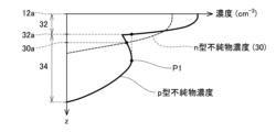
- FIG. 6 shows the impurity concentration distribution in the z direction in the source layer 30, the contact layer 32, and the body layer 34.
- the lower end 30a of the source layer 30 is defined as the position where the n-type impurity concentration and the p-type impurity concentration are the same.
- the body layer 34 i.e., the p-type region below the source layer 30
- the p-type impurity concentration is distributed in a normal distribution having a peak value P1.
- the contact layer 32 is defined as a p-type layer having a p-type impurity concentration higher than the peak value P1.
- the lower end 32a of the contact layer 32 is defined as a position having the same p-type impurity concentration as the peak value P1. As shown in FIG. 6, the lower end 32a of the contact layer 32 is located above the lower end 30a of the source layer 30.
- the MOSFET 10 When a potential equal to or higher than the gate threshold is applied to each gate electrode 18, a channel is formed in the body layer 34 near the gate insulating film 16. The channel connects the source layer 30 and the drift layer 38.
- the potential of the drain electrode 24 is higher than the potential of the source electrode 22, electrons flow from the source layer 30 to the drain layer 40 via the channel and the drift layer 38. That is, the MOSFET 10 is turned on.
- the potential of each gate electrode 18 is lowered to a value lower than the gate threshold, the channel disappears and the flow of electrons stops. That is, the MOSFET 10 is turned off.
- a depletion layer extends from the body layer 34 to the drift layer 38.
- a depletion layer also extends from the deep layer 36 and the trench lower layer 35 to the drift layer 38.
- the depletion layer extending from the deep layer 36 and the trench lower layer 35 promotes depletion in the semiconductor region around the lower end of the trench 14. This prevents electric field concentration on the gate insulating film 16.
- a potential higher than that of the drain electrode 24 may be applied to the source electrode 22.
- a diode formed by a pn junction at the interface between the p-type layer i.e., a p-type layer formed by the body layer 34, the trench lower layer 35, and the deep layer 36
- the drift layer 38 is turned on. That is, holes flow from the p-type layer to the drift layer 38, and electrons flow from the drift layer 38 to the p-type layer.
- FIG. 7 shows the change in the drain-source voltage Vds and the drain current Ids during the recovery operation.
- a depletion layer develops from the pn junction at the interface between the p-type layer and the drift layer 38 into the drift layer, and holes in the drift layer 38 are discharged to the source electrode 22 via the p-type layer.
- a recovery current IR flows as shown in FIG. 7.
- a surge voltage Vak occurs between the source electrode 22 and the drain electrode 24.
- the deep layer 36 protrudes toward the drift layer 38, holes are likely to flow from the drift layer 38 into the deep layer 36 during recovery operation. Therefore, as shown by the arrow 100 in FIG.
- holes are discharged from the drift layer 38 to the source electrode 22 through the deep layer 36, the body layer 34, and the contact layer 32.
- the contact layer 32 does not exist above the deep layer 36, holes that pass through the deep layer 36 move laterally in the body layer 34 and then flow to the contact layer 32. Therefore, the resistance of the path through which the holes flow is high. Therefore, the recovery current IR is suppressed, and the surge voltage Vak is suppressed.
- the depletion layer also extends from the pn junction into the p-type layer. Holes discharged from the depleted p-type layer to the source electrode 22 also constitute the recovery current.
- the depletion layer extends from the pn junction toward the upper side. When the depletion layer reaches the lower end 30a of the source layer 30, the depletion layer stops extending upward.
- the lower end 32a of the contact layer 32 is located above the lower end 30a of the source layer 30, so that the depletion layer is prevented from extending into the contact layer 32. Therefore, the high concentration of holes in the contact layer 32 is prevented from being discharged to the source electrode 22 as a recovery current.
- FIG. 8 shows the relationship between the depth D of the contact layer 32 and the surge voltage Vak.
- the depth D refers to the relative position in the z direction of the lower end 32a of the contact layer 32 with respect to the lower end 30a of the source layer 30.
- a positive depth D means that the lower end 32a of the contact layer 32 is located higher than the lower end 30a of the source layer 30.
- the greater the depth D i.e., the higher the lower end 32a of the contact layer 32 is located), the more the surge voltage Vak is suppressed.
- the MOSFET 10 of the embodiment can suppress the recovery current.
- the lower end 32a of the contact layer 32 is located above the lower end 30a of the source layer 30.
- the lower end 32a of the contact layer 32 may be located at the same position as the lower end 30a of the source layer 30.
- the depth D may be zero. As shown in FIG. 8, even when the depth D is zero, the surge voltage Vak is suppressed compared to when the depth D is negative.
- the contact layer 32 does not exist on the deep layer 36.
- a part 32x of the contact layer 32 may be disposed on the deep layer 36. That is, when the semiconductor substrate 12 is viewed from above, the part 32x of the contact layer 32 may overlap the deep layer 36.
- FIG. 10 shows the relationship between the width W (see FIG. 9) of the overlapping part of the contact layer 32 and the deep layer 36 and the reduction rate of the surge voltage Vak.
- a negative width W means that the contact layer 32 and the deep layer 36 do not overlap.
- the width Wd means the width of the deep layer 36 in the y direction (see FIG. 9).
- the surge voltage Vak decreases as the width W decreases from 1/2Wd.
- the spacing portion 33 is disposed above the deep layer 36, so that the resistance of the recovery current path can be increased and the recovery current can be suppressed.
- a contact layer 32 was provided for each gap 37 of the deep layer 36.
- the source layer 30 is provided in the entire area where the contact layer 32 is not present in the surface layer portion near the upper surface 12a.
- the distribution range of the source layer 30 may be narrower.
- Figures 12 and 13 show an example in which the distribution range of the source layer 30 is narrower than that of Figure 5.
- the hatched region R indicates an area on the upper surface 12a where neither the contact layer 32 nor the source layer 30 is arranged.
- region R the body layer 34 is in contact with the source electrode 22 on the upper surface 12a.
- the source layer 30 is provided only in the area adjacent to the trench 14.
- the body layer 34 i.e., region R
- the source layer 30 is provided in the area adjacent to the end of the contact layer 32 in the x direction, and the source layer 30 is provided in the other area.
- each deep layer 36 extends long in the x direction when the semiconductor substrate 12 is viewed from above.
- each deep layer 36 may be provided distributed in the x direction when the semiconductor substrate 12 is viewed from above.
- the deep layers 36 are provided distributed in the x direction so that the deep layers 36 are present in each inter-trench region 50. Within each inter-trench region 50, the deep layers 36 are arranged at intervals in the y direction. The configuration in FIG. 14 can also suppress the recovery current.
- (Configuration 1) A field effect transistor, A semiconductor substrate made of a compound semiconductor and having a plurality of trenches on an upper surface thereof; a plurality of gate electrodes each disposed in a corresponding one of the trenches and insulated from the semiconductor substrate by a gate insulating film; a source electrode in contact with an upper surface of the semiconductor substrate; having the semiconductor substrate has a plurality of n-type source layers, a plurality of p-type contact layers, a p-type body layer, an n-type drift layer, and a plurality of p-type deep layers; Each semiconductor region located between the plurality of trenches in the semiconductor substrate is an inter-trench region; Each of the source layers is disposed in a corresponding one of the inter-trench regions, contacts the source electrode, and contacts a corresponding one of the gate insulating films; Each of the contact layers is disposed in a corresponding one of the inter-trench regions and contacts the source electrode; A plurality of n-type source layers, a p
- Field effect transistor (Configuration 2) 2. The field effect transistor of claim 1, wherein each of said deep layers intersects each of said trenches when viewed from above said semiconductor substrate. (Configuration 3) 3. The field effect transistor according to claim 1, wherein the contact layers and the deep layers do not overlap each other when viewed from above the semiconductor substrate. (Configuration 4) A field effect transistor according to any one of configurations 1 to 3, wherein in each inter-trench region, the gap of the deep layer has a first gap that overlaps with the contact layer when the semiconductor substrate is viewed from above, and a second gap that does not overlap with the contact layer when the semiconductor substrate is viewed from above. (Configuration 5) 5. The field effect transistor according to any one of configurations 1 to 4, wherein, in the thickness direction of the semiconductor substrate, the lower ends of the contact layers are located at the same position as or higher than the lower ends of the source layers.
Landscapes
- Electrodes Of Semiconductors (AREA)
- Insulated Gate Type Field-Effect Transistor (AREA)
Priority Applications (1)
| Application Number | Priority Date | Filing Date | Title |
|---|---|---|---|
| CN202480041184.8A CN121549072A (zh) | 2023-07-31 | 2024-05-20 | 场效应晶体管 |
Applications Claiming Priority (2)
| Application Number | Priority Date | Filing Date | Title |
|---|---|---|---|
| JP2023124922A JP2025021163A (ja) | 2023-07-31 | 2023-07-31 | 電界効果トランジスタ |
| JP2023-124922 | 2023-07-31 |
Related Child Applications (1)
| Application Number | Title | Priority Date | Filing Date |
|---|---|---|---|
| US19/424,818 Continuation US20260129956A1 (en) | 2023-07-31 | 2025-12-18 | Field-effect transistor |
Publications (1)
| Publication Number | Publication Date |
|---|---|
| WO2025027977A1 true WO2025027977A1 (ja) | 2025-02-06 |
Family
ID=94395044
Family Applications (1)
| Application Number | Title | Priority Date | Filing Date |
|---|---|---|---|
| PCT/JP2024/018533 Pending WO2025027977A1 (ja) | 2023-07-31 | 2024-05-20 | 電界効果トランジスタ |
Country Status (3)
| Country | Link |
|---|---|
| JP (1) | JP2025021163A (https=) |
| CN (1) | CN121549072A (https=) |
| WO (1) | WO2025027977A1 (https=) |
Citations (5)
| Publication number | Priority date | Publication date | Assignee | Title |
|---|---|---|---|---|
| JP2001267570A (ja) | 2000-03-15 | 2001-09-28 | Mitsubishi Electric Corp | 半導体装置及び半導体装置製造方法 |
| JP2014045223A (ja) * | 2011-04-12 | 2014-03-13 | Denso Corp | 半導体装置の製造方法 |
| WO2020202430A1 (ja) * | 2019-04-01 | 2020-10-08 | 三菱電機株式会社 | 半導体装置 |
| JP7169459B2 (ja) * | 2019-10-11 | 2022-11-10 | 株式会社デンソー | スイッチング素子 |
| JP2023005786A (ja) * | 2021-06-29 | 2023-01-18 | 株式会社豊田中央研究所 | 半導体装置 |
-
2023
- 2023-07-31 JP JP2023124922A patent/JP2025021163A/ja active Pending
-
2024
- 2024-05-20 CN CN202480041184.8A patent/CN121549072A/zh active Pending
- 2024-05-20 WO PCT/JP2024/018533 patent/WO2025027977A1/ja active Pending
Patent Citations (5)
| Publication number | Priority date | Publication date | Assignee | Title |
|---|---|---|---|---|
| JP2001267570A (ja) | 2000-03-15 | 2001-09-28 | Mitsubishi Electric Corp | 半導体装置及び半導体装置製造方法 |
| JP2014045223A (ja) * | 2011-04-12 | 2014-03-13 | Denso Corp | 半導体装置の製造方法 |
| WO2020202430A1 (ja) * | 2019-04-01 | 2020-10-08 | 三菱電機株式会社 | 半導体装置 |
| JP7169459B2 (ja) * | 2019-10-11 | 2022-11-10 | 株式会社デンソー | スイッチング素子 |
| JP2023005786A (ja) * | 2021-06-29 | 2023-01-18 | 株式会社豊田中央研究所 | 半導体装置 |
Also Published As
| Publication number | Publication date |
|---|---|
| CN121549072A (zh) | 2026-02-17 |
| JP2025021163A (ja) | 2025-02-13 |
Similar Documents
| Publication | Publication Date | Title |
|---|---|---|
| JP7537377B2 (ja) | 電界効果トランジスタとその製造方法 | |
| US9093493B2 (en) | Wide bandgap insulated gate semiconductor device | |
| US10276654B2 (en) | Semiconductor device with parallel PN structures | |
| JP2019087611A (ja) | スイッチング素子とその製造方法 | |
| US20230369484A1 (en) | Field effect transistor | |
| CN115706166B (zh) | 场效应晶体管及其制造方法 | |
| JP7600848B2 (ja) | 半導体装置 | |
| US11264451B2 (en) | Semiconductor device exhibiting soft recovery characteristics | |
| WO2021100206A1 (ja) | スイッチング素子 | |
| US20240321951A1 (en) | Field effect transistor | |
| JP2024107477A (ja) | 電界効果トランジスタ | |
| US20230299144A1 (en) | Silicon carbide semiconductor device | |
| WO2025027977A1 (ja) | 電界効果トランジスタ | |
| WO2024042814A1 (ja) | 電界効果トランジスタ | |
| JP7560344B2 (ja) | 半導体装置 | |
| US20260129956A1 (en) | Field-effect transistor | |
| JP2024072452A (ja) | 半導体装置 | |
| JP7827117B2 (ja) | 半導体装置 | |
| US20250301724A1 (en) | Switching element | |
| US20240313107A1 (en) | Semiconductor device | |
| US20250107187A1 (en) | Switching element | |
| WO2025248712A1 (ja) | スイッチング素子 | |
| JP2024085757A (ja) | 半導体装置 | |
| JP2024131786A (ja) | 半導体装置 | |
| WO2024084778A1 (ja) | 半導体装置とその製造方法 |
Legal Events
| Date | Code | Title | Description |
|---|---|---|---|
| WWE | Wipo information: entry into national phase |
Ref document number: 2024848638 Country of ref document: EP |
|
| NENP | Non-entry into the national phase |
Ref country code: DE |