WO2025027927A1 - 圧電振動素子 - Google Patents
圧電振動素子 Download PDFInfo
- Publication number
- WO2025027927A1 WO2025027927A1 PCT/JP2024/010616 JP2024010616W WO2025027927A1 WO 2025027927 A1 WO2025027927 A1 WO 2025027927A1 JP 2024010616 W JP2024010616 W JP 2024010616W WO 2025027927 A1 WO2025027927 A1 WO 2025027927A1
- Authority
- WO
- WIPO (PCT)
- Prior art keywords
- excitation electrode
- electrode
- dle
- thickness
- dwe
- Prior art date
- Legal status (The legal status is an assumption and is not a legal conclusion. Google has not performed a legal analysis and makes no representation as to the accuracy of the status listed.)
- Pending
Links
Images


Classifications
-
- H—ELECTRICITY
- H03—ELECTRONIC CIRCUITRY
- H03H—IMPEDANCE NETWORKS, e.g. RESONANT CIRCUITS; RESONATORS
- H03H9/00—Networks comprising electromechanical or electro-acoustic elements; Electromechanical resonators
- H03H9/15—Constructional features of resonators consisting of piezoelectric or electrostrictive material
- H03H9/17—Constructional features of resonators consisting of piezoelectric or electrostrictive material having a single resonator
- H03H9/19—Constructional features of resonators consisting of piezoelectric or electrostrictive material having a single resonator consisting of quartz
-
- H—ELECTRICITY
- H03—ELECTRONIC CIRCUITRY
- H03H—IMPEDANCE NETWORKS, e.g. RESONANT CIRCUITS; RESONATORS
- H03H9/00—Networks comprising electromechanical or electro-acoustic elements; Electromechanical resonators
- H03H9/02—Details
- H03H9/02007—Details of bulk acoustic wave devices
- H03H9/02157—Dimensional parameters, e.g. ratio between two dimension parameters, length, width or thickness
-
- H—ELECTRICITY
- H03—ELECTRONIC CIRCUITRY
- H03H—IMPEDANCE NETWORKS, e.g. RESONANT CIRCUITS; RESONATORS
- H03H9/00—Networks comprising electromechanical or electro-acoustic elements; Electromechanical resonators
- H03H9/02—Details
- H03H9/05—Holders or supports
- H03H9/10—Mounting in enclosures
- H03H9/1007—Mounting in enclosures for bulk acoustic wave [BAW] devices
- H03H9/1014—Mounting in enclosures for bulk acoustic wave [BAW] devices the enclosure being defined by a frame built on a substrate and a cap, the frame having no mechanical contact with the BAW device
- H03H9/1021—Mounting in enclosures for bulk acoustic wave [BAW] devices the enclosure being defined by a frame built on a substrate and a cap, the frame having no mechanical contact with the BAW device the BAW device being of the cantilever type
-
- H—ELECTRICITY
- H03—ELECTRONIC CIRCUITRY
- H03H—IMPEDANCE NETWORKS, e.g. RESONANT CIRCUITS; RESONATORS
- H03H9/00—Networks comprising electromechanical or electro-acoustic elements; Electromechanical resonators
- H03H9/02—Details
- H03H9/05—Holders or supports
- H03H9/10—Mounting in enclosures
- H03H9/1007—Mounting in enclosures for bulk acoustic wave [BAW] devices
- H03H9/1035—Mounting in enclosures for bulk acoustic wave [BAW] devices the enclosure being defined by two sealing substrates sandwiching the piezoelectric layer of the BAW device
-
- H—ELECTRICITY
- H03—ELECTRONIC CIRCUITRY
- H03H—IMPEDANCE NETWORKS, e.g. RESONANT CIRCUITS; RESONATORS
- H03H9/00—Networks comprising electromechanical or electro-acoustic elements; Electromechanical resonators
- H03H9/02—Details
- H03H9/125—Driving means, e.g. electrodes, coils
- H03H9/13—Driving means, e.g. electrodes, coils for networks consisting of piezoelectric or electrostrictive materials
- H03H9/131—Driving means, e.g. electrodes, coils for networks consisting of piezoelectric or electrostrictive materials consisting of a multilayered structure
-
- H—ELECTRICITY
- H03—ELECTRONIC CIRCUITRY
- H03H—IMPEDANCE NETWORKS, e.g. RESONANT CIRCUITS; RESONATORS
- H03H9/00—Networks comprising electromechanical or electro-acoustic elements; Electromechanical resonators
- H03H9/02—Details
- H03H9/125—Driving means, e.g. electrodes, coils
- H03H9/13—Driving means, e.g. electrodes, coils for networks consisting of piezoelectric or electrostrictive materials
- H03H9/132—Driving means, e.g. electrodes, coils for networks consisting of piezoelectric or electrostrictive materials characterized by a particular shape
-
- H—ELECTRICITY
- H03—ELECTRONIC CIRCUITRY
- H03H—IMPEDANCE NETWORKS, e.g. RESONANT CIRCUITS; RESONATORS
- H03H9/00—Networks comprising electromechanical or electro-acoustic elements; Electromechanical resonators
- H03H9/15—Constructional features of resonators consisting of piezoelectric or electrostrictive material
- H03H9/17—Constructional features of resonators consisting of piezoelectric or electrostrictive material having a single resonator
- H03H9/177—Constructional features of resonators consisting of piezoelectric or electrostrictive material having a single resonator of the energy-trap type
Definitions
- the present invention relates to a piezoelectric vibration element.
- Piezoelectric vibration elements are used as timing devices, sensors, oscillators, etc. in various electronic devices such as mobile communication terminals, communication base stations, and home appliances.
- a piezoelectric vibration element comprises a piezoelectric piece having a pair of main surfaces, and a pair of excitation electrodes provided on the pair of main surfaces of the piezoelectric piece.
- Patent Document 1 discloses a vibration element that includes a substrate that vibrates with thickness-shear vibration and includes a first main surface and a second main surface that are in a front-back relationship, a first excitation electrode provided on the first main surface, and a second excitation electrode provided on the second main surface that is larger than the first excitation electrode in a planar view, and the first excitation electrode is disposed so as to be contained within the outer edge of the second excitation electrode in a planar view.
- the present invention was made in consideration of these circumstances, and aims to provide a piezoelectric vibration element that can improve the electromechanical coupling coefficient.
- a piezoelectric vibration element comprises a piezoelectric piece having a first main surface and a second main surface opposite the first main surface, a first excitation electrode provided on the first main surface, and a second excitation electrode provided on the second main surface, in which, in a plan view in the opposing direction in which the first main surface and the second main surface face each other, the area of the second excitation electrode is larger than the area of the first excitation electrode, a portion of the second excitation electrode overlaps with the entirety of the first excitation electrode, and the thickness of the second excitation electrode along the opposing direction is larger than the thickness of the first excitation electrode along the opposing direction.
- a piezoelectric vibration element includes a piezoelectric piece having a first main surface and a second main surface facing the first main surface, a first excitation electrode provided on the first main surface, a second excitation electrode provided on the second main surface, and an insulating film laminated on the second excitation electrode, in which, in a plan view in the opposing direction in which the first main surface and the second main surface face each other, the area of the laminate consisting of the second excitation electrode and the insulating film is larger than the area of the first excitation electrode, and a part of the laminate overlaps with the entire first excitation electrode, and the sum of the thickness of the second excitation electrode and the thickness of the insulating film along the opposing direction is larger than the thickness of the first excitation electrode along the opposing direction.
- the present invention provides a piezoelectric vibration element that can improve the electromechanical coupling coefficient.
- FIG. 2 is an exploded perspective view of the crystal resonator according to the first embodiment.
- FIG. 2 is a plan view of a vibration section according to the first embodiment.
- 3 is a cross-sectional view of a vibration section according to the first embodiment.
- FIG. 6 is a graph showing a simulation result based on the first embodiment.
- 11 is a cross-sectional view showing a state in which a positional deviation occurs in a first excitation electrode.
- FIG. 6 is a graph showing a simulation result based on the first embodiment.
- 6 is a graph showing a simulation result based on the first embodiment.
- 6 is a graph showing a simulation result based on the first embodiment.
- 6 is a graph showing a simulation result based on the first embodiment.
- 6 is a graph showing a simulation result based on the first embodiment.
- 6 is a graph showing a simulation result based on the first embodiment.
- FIG. 11 is a plan view of a vibration section according to a second embodiment.
- FIG. 11 is a cross-sectional view of a vibration section according to a second embodiment.
- FIG. 11 is a perspective view showing a configuration of a vibration section according to a third embodiment.
- 13A and 13B are diagrams illustrating vibration distribution of a vibration section according to the third embodiment.
- 13 is a graph showing a simulation result based on the third embodiment.
- 13 is a graph showing a simulation result based on the third embodiment.
- FIG. 13 is a perspective view showing a configuration of a vibration section according to a fourth embodiment.
- FIG. 13 is a diagram showing a vibration distribution of a vibration section according to a fourth embodiment;
- FIG. 13 is a cross-sectional view of a vibration part according to a fifth embodiment.
- FIG. 13 is a cross-sectional view of a vibration part according to a sixth embodiment.
- FIG. 23 is a cross-sectional view of a vibration part according to the seventh embodiment.
- FIG. 23 is a cross-sectional view of a vibration part according to the eighth embodiment.
- an orthogonal coordinate system consisting of the X-axis, Y'-axis, and Z'-axis may be conveniently attached to each drawing.
- the X-axis, Y'-axis, and Z'-axis correspond to each other in each drawing.
- the X-axis, Y'-axis, and Z'-axis each correspond to the crystallographic axes of the quartz piece 11, which will be described later.
- the X-axis corresponds to the electrical axis (polarity axis) of the quartz
- the Y-axis corresponds to the mechanical axis of the quartz
- the Z-axis corresponds to the optical axis of the quartz.
- the Y'-axis and Z'-axis are axes obtained by rotating the Y-axis and Z-axis counterclockwise around the X-axis by ⁇ degrees when viewed from the positive direction of the X-axis.
- the direction parallel to the X-axis is referred to as the "X-axis direction”
- the direction parallel to the Y'-axis is referred to as the “Y'-axis direction”
- the direction parallel to the Z'-axis is referred to as the "Z'-axis direction”.
- the directions of the tips of the arrows on the X-axis, Y'-axis, and Z'-axis are referred to as "positive” or "+ (plus)”
- the directions opposite the arrows are referred to as "negative” or "- (minus)”.
- the +Y'-axis direction is described as the upward direction
- the -Y'-axis direction is described as the downward direction
- the up-down orientation of the quartz crystal vibrating element 10 and the quartz crystal vibrator 1 is not limited to this.
- the plane specified by the X-axis and Z'-axis is referred to as the Z'X plane, and the same applies to the planes specified by the other axes.
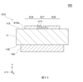
- Fig. 1 is an exploded perspective view of the quartz crystal resonator according to the first embodiment.
- Fig. 2 is a plan view of the vibration part according to the first embodiment.
- Fig. 3 is a cross-sectional view of the vibration part according to the first embodiment. Note that Fig. 3 is a cross-sectional view taken along line III-III of the vibration part shown in Fig. 2.
- the quartz crystal resonator 1 comprises a quartz crystal resonator element 10, a bottom cover 20, a top cover 30, a bottom joint 40, and a top joint 50.
- the bottom cover 20, the quartz crystal resonator element 10, and the top cover 30 are arranged in this order with a gap in between in the Y'-axis direction.
- the Y'-axis direction in which the bottom cover 20, the quartz crystal resonator element 10, and the top cover 30 are stacked is referred to as the "thickness direction.”
- the Y'-axis direction is an example of the "opposition direction.”
- the crystal unit 1 is used, for example, as a component of a temperature compensated crystal oscillator (TCXO), a voltage controlled crystal oscillator (VCXO), or an oven controlled crystal oscillator (OCXO).
- TCXO temperature compensated crystal oscillator
- VCXO voltage controlled crystal oscillator
- OCXO oven controlled crystal oscillator
- the quartz crystal vibration element 10 is an electromechanical energy conversion element that converts electrical energy into mechanical energy and vice versa through the piezoelectric effect. As shown in FIG. 1, the quartz crystal vibration element 10 has a vibration part 110, a holding part 120, and a support arm 130.
- the vibration part 110 is excited at a predetermined frequency based on the applied alternating voltage.
- the vibration part 110 is held in a vibration space between the lower cover 20 and the upper cover 30 so that it can vibrate.
- the main vibration of the vibration part 110 is a thickness shear vibration mode.
- the shape of the vibration part 110 when the XZ' plane is viewed in a plane (hereinafter simply referred to as "planar view") (hereinafter referred to as "planar shape”) is a rectangle having a pair of short sides 111, 112 and a pair of long sides 113, 114.
- the pair of short sides 111, 112 extend along the Z' axis direction and face each other in the X axis direction.
- the pair of long sides 113, 114 extend along the X axis direction and face each other outward in the Z' axis direction.
- the main vibration of the vibrating part is not limited to thickness-slip vibration mode, and may be, for example, thickness-extension vibration mode, expansion vibration mode, length vibration mode, or bending vibration mode.
- the planar shape of the vibrating part is not limited to rectangular, and may be, for example, square, polygonal, circular, elliptical, or a combination of these.
- the holding portion 120 is a portion for holding the vibration portion 110.
- the holding portion 120 together with the lower cover 20, the upper cover 30, the lower joint portion 40, and the upper joint portion 50, form a vibration space for the vibration portion 110.
- the holding portion 120 is spaced apart from the vibration portion 110 and is provided in a frame shape surrounding the vibration portion 110.
- the holding portion 120 has frame portions 121A, 121B, 121C, and 121D.
- the frame portions 121A, 121B, 121C, and 121D are each a part of a substantially rectangular frame surrounding the vibration portion 110. As shown in FIG. 1 and FIG. 2, the frame portion 121A is spaced apart from the short side 111 of the vibration portion 110 in the X-axis direction and extends parallel to the short side 111 along the Z'-axis direction. The frame portion 121B is spaced apart from the short side 112 of the vibration portion 110 in the X-axis direction and extends parallel to the short side 112 along the Z'-axis direction. The frame portion 121C is spaced apart from the long side 113 of the vibration portion 110 in the Z'-axis direction and extends parallel to the long side 113 along the X-axis direction. The frame portion 121D is spaced apart from the long side 114 of the vibration portion 110 in the Z'-axis direction and extends parallel to the long side 114 along the X-axis direction.
- Both ends of frame portion 121C are connected to one end of frame portion 121A and one end of frame portion 121B, respectively. Both ends of frame portion 121D are connected to the other end of frame portion 121A and the other end of frame portion 121B, respectively.
- Frame portion 121A and frame portion 121B face each other in the X-axis direction, sandwiching vibration portion 110 therebetween.
- Frame portion 121C and frame portion 121D face each other in the Z'-axis direction, sandwiching vibration portion 110 therebetween.
- the holding portion need only be provided around at least a portion of the periphery of the vibrating portion, and is not limited to a frame-like shape.
- the holding portion may be provided in the shape of a rail having two parallel frame portions.
- the support arm 130 supports the vibration part 110 and allows the holding part 120 to hold the vibration part 110.
- the support arm 130 connects the vibration part 110 and the holding part 120. As shown in Figures 1 and 2, the support arm 130 connects the end of the vibration part 110 on the short side 112 side to the frame part 121B of the holding part 120.
- the support arm 130 extends along the X-axis.
- the bottom cover 20 faces the vibration part 110, the holding part 120, and the support arm 130 of the quartz crystal vibration element 10 with a gap in the Y'-axis direction.
- the bottom cover 20 is provided in a flat plate shape. As shown in FIG. 1, when viewed in a plan view, the bottom cover 20 has a pair of long sides that extend along the X-axis direction and face each other in the Z'-axis direction, and a pair of short sides that extend along the Z'-axis direction and face each other in the Z-axis direction.
- the pair of long sides and the pair of short sides of the bottom cover 20 are connected by sides that are inclined relative to the pair of long sides and the pair of short sides. In other words, notches are formed in the four corners of the bottom cover 20 when viewed in a plan view.
- the top cover 30 faces the vibration part 110, the holding part 120, and the support arm 130 of the quartz crystal vibration element 10 at a distance in the Y'-axis direction on the opposite side to the bottom cover 20.
- the top cover 30 is provided in a flat plate shape. As shown in FIG. 1, when viewed in a plan view, the top cover 30 has a pair of long sides that extend along the X-axis direction and face each other in the Z'-axis direction, and a pair of short sides that extend along the Z'-axis direction and face each other in the Z-axis direction.
- the planar shape of the top cover 30 is rectangular.
- the lower joint 40 and the upper joint 50 are provided in a frame shape along the holding portion 120 of the quartz vibration element 10.
- the lower joint 40 joins the holding portion 120 of the quartz vibration element 10 to the end of the lower cover 20.
- the upper joint 50 joins the holding portion 120 of the quartz vibration element 10 to the end of the upper cover 30.
- the lower joint 40 and the upper joint 50 are provided by an organic adhesive containing, for example, an epoxy-based, vinyl-based, acrylic-based, urethane-based, or silicone-based resin.
- the material of the lower joint and the upper joint is not limited to organic adhesives, and may be inorganic adhesives such as silicon-based adhesives containing water glass, calcium-based adhesives containing cement, etc.
- the material of the lower joint and the upper joint may be low-melting glass (e.g., lead borate-based or tin phosphate-based).
- the material of the lower joint and the upper joint may be gold (Au), tin (Sn), copper (Cu), titanium (Ti), aluminum (Al), germanium (Ge), silicon (Si), or a eutectic alloy containing at least one of these.
- the quartz crystal vibration element 10 includes a quartz crystal blank 11, a first excitation electrode 14a, a second excitation electrode 14b, a first extraction electrode 15a, a second extraction electrode 15b, a first connection electrode 16a, and a second connection electrode 16b.
- the quartz piece 11 is a type of piezoelectric piece made of a piezoelectric material that vibrates in response to an applied voltage.
- the quartz piece 11 is provided continuously across the vibrating part 110, the holding part 120, and the support arm 130. In the XZ' plane direction, the quartz piece 11 extends over almost the entire area of each of the vibrating part 110, the holding part 120, and the support arm 130.
- the quartz piece 11 is a thin quartz crystal with the XZ' plane as its main surface.
- the quartz crystal piece 11 is, for example, an AT-cut quartz crystal piece. That is, the counterclockwise rotation angle ⁇ of the Z'-axis and Y'-axis from the Z-axis and Y-axis when viewed from the positive side of the X-axis is 35 degrees 15 minutes ⁇ 1 minute 30 seconds.
- the quartz crystal vibration element 10 using the AT-cut quartz crystal piece 11 has high frequency stability over a wide temperature range.
- the cut angle of the quartz piece is not limited to the above.
- the rotation angle of the Y'-axis and Z'-axis in the AT-cut quartz piece 11 may be tilted in the range of -5 degrees or more or +15 degrees or less from 35 degrees 15 minutes.
- the cut angle of the quartz piece may also be a different cut other than the AT cut, such as a BT cut, a GT cut, or an SC cut.
- the planar shape of the quartz piece 11 in the vibrating part 110 is a rectangle with a long side along the X-axis direction and a short side along the Z'-axis direction.
- the quartz piece 11 has an upper surface 11A provided on the upper cover 30 side and a lower surface 11B provided on the lower cover 20 side.
- the upper surface 11A and the lower surface 11B correspond to an example of a pair of main surfaces of the quartz piece 11 that face each other in the Y'-axis direction.
- the planar shape of the vibrating part of the quartz piece is not limited to the above.
- the planar shape of the vibrating part of the quartz piece may be a rectangle having a long side extending in the Z'-axis direction and a short side extending in the X-axis direction, or a rectangle having a short side extending in the Z'-axis direction and a long side extending in the X-axis direction.
- the planar shape of the vibrating part of the quartz piece may be a polygon, a circle, an ellipse, or a combination of these.
- the vibrating part of the quartz piece is not limited to a flat plate shape.
- the vibrating part of the quartz piece may have a mesa structure or an inverted mesa structure with unevenness on at least one of the upper and lower surfaces.
- the vibrating part of the quartz piece may have a convex structure in which the amount of change in thickness changes continuously, or a bevel structure in which the amount of change in thickness changes discontinuously.
- the first excitation electrode 14a and the second excitation electrode 14b apply an alternating voltage to the crystal piece 11 of the vibrating part 110 to excite the vibrating part 110.
- the first excitation electrode 14a is provided on the upper surface 11A of the crystal piece 11 in the vibrating part 110
- the second excitation electrode 14b is provided on the lower surface 11b of the crystal piece 11 in the vibrating part 110.
- the first excitation electrode 14a and the second excitation electrode 14b face each other in the Y'-axis direction with the crystal piece 11 in between.
- the area of the second excitation electrode 14b is larger than the area of the first excitation electrode 14a, and a part of the second excitation electrode 14b overlaps with the entirety of the first excitation electrode 14a.
- the first excitation electrode 14a and the second excitation electrode 14b are provided in the center of the vibration part 110, and the center of the first excitation electrode 14a overlaps with the center of the second excitation electrode 14b.
- the positions of the first excitation electrode and the second excitation electrode are not limited to the center of the vibration section. In a plan view, the first excitation electrode and the second excitation electrode may be provided outward from the center of the vibration section. Furthermore, the positions of the centers of the first excitation electrode and the second excitation electrode are not limited to overlapping positions. In a plan view, the center of the first excitation electrode may be separated from the center of the second excitation electrode.
- the planar shape of the first excitation electrode 14a is a rectangle having short sides extending in the Z'-axis direction and long sides extending in the X-axis direction.
- the planar shape of the second excitation electrode 14b is similar to that of the first excitation electrode 14a.
- the first excitation electrode 14a and the second excitation electrode 14b have short sides parallel to the short sides of the vibration part 110 and short sides parallel to the long sides of the vibration part 110.
- the first excitation electrode 14a and the second excitation electrode 14b have a thickness in the Y'-axis direction, and the thickness of the second excitation electrode 14b is greater than the thickness of the first excitation electrode 14a.
- the planar shapes of the first excitation electrode and the second excitation electrode are not limited to the above.
- the planar shapes of the first excitation electrode and the second excitation electrode may be rectangular with short sides extending in the X-axis direction.
- the planar shapes of the first excitation electrode and the second excitation electrode may be square, polygonal, circular, elliptical, or a combination of these.
- the planar shape of the first excitation electrode is not limited to being the same as the planar shape of the second excitation electrode, and the planar shapes of the first excitation electrode and the second excitation electrode may be different from each other.
- the first extraction electrode 15a electrically connects the first excitation electrode 14a and the first connection electrode 16a. As shown in FIG. 1, the first extraction electrode 15a extracted from the first excitation electrode 14a extends over the upper surface of the vibration part 110, the support arm 130, and the frame part 121B of the holding part 120, as well as the side of the holding part 120, and is electrically connected to the first connection electrode 16a provided on the lower surface of the holding part 120.
- the second extraction electrode 15b extracted from the second excitation electrode 14b extends over the lower surface, side and upper surface of the vibration part 110, the support arm 130, the upper surface of the frame parts 121B and 121D of the holding part 120, as well as the side of the holding part 120, and is electrically connected to the second connection electrode 16b provided on the lower surface of the holding part 120.
- the first connection electrode 16a electrically connects the first excitation electrode 14a to an external terminal
- the second connection electrode 16b electrically connects the second excitation electrode 14b to an external terminal.
- the first connection electrode 16a is provided on the underside (the surface on the lower cover 20 side) of the crystal piece 11 at the corner of the holding portion 120 where the frame portion 121B and the frame portion 121C are connected.
- the second connection electrode 16b is provided on the underside of the crystal piece 11 at the corner of the holding portion 120 where the frame portion 121A and the frame portion 121D are connected.
- the first excitation electrode 14a, the first extraction electrode 15a, and the first connection electrode 16a are integrally provided.
- These electrodes of the quartz crystal vibration element 10 have a single-layer structure made of an aluminum layer, for example.
- the electrodes of the quartz crystal vibration element 10 may have a multi-layer structure in which a base layer and a surface layer are laminated in this order.
- the base layer is a chromium (Cr) layer that has good adhesion to the quartz crystal blank 11, and the surface layer is a gold (Au) layer that has good chemical stability.
- the electrodes of the quartz crystal vibration element 10 may contain silver (Ag), copper (Cu), titanium (Ti), molybdenum (Mo), or an aluminum-copper alloy (AlCu).
- the bottom cover 20 has a crystal blank 21, power terminals ST1 and ST2, and dummy terminals DT1 and DT2.
- the crystal blank 21 is a flat substrate that overlaps with almost the entire crystal vibration element 10 in a planar view.
- the crystal blank 21 is formed of a crystal crystal with the same cut angle as the crystal blank 11 of the crystal vibration element 10. This can reduce thermal stress caused by differences in thermal expansion coefficients and differences in the directions of thermal expansion and contraction between the crystal vibration element 10 and the bottom cover 20. This can suppress fluctuations in the frequency of the crystal vibration element 10.
- the crystal blank 21 has an upper surface 21A provided on the crystal vibration element 10 side and a lower surface 21B provided on the opposite side to the upper surface 21A.
- the crystal blank 21 When viewed in a planar view, the crystal blank 21 has a long side extending along the X-axis direction and a short side extending along the Z'-axis direction.
- the side surface connecting the upper surface 21A and the lower surface 21B of the quartz crystal piece 21 overlaps with the outer side surface of the holding portion 120 of the quartz crystal vibrating element 10.
- a notch is formed at the corner where the short side and long side of the quartz crystal piece 21 connect.
- the area of the quartz crystal piece 21 in a plan view is smaller than the area of the quartz crystal piece 31 in a plan view, described below, by the amount of this notch.
- the shape of the side surface formed by the notch at the corner of the quartz crystal piece 21 is, for example, planar. However, the shape of the side surface formed by the notch at the corner of the quartz crystal piece 21 is not limited to this, and may be a curved surface that is part of a cylinder or a rectangular prism.
- the power terminals ST1, ST2 and the dummy terminals DT1, DT2 are provided on the lower surface 21B of the crystal blank 21.
- the power terminals ST1, ST2 and the dummy terminals DT1, DT2 correspond to an example of an external terminal of the crystal resonator 1.
- the power terminals ST1, ST2 are for applying a drive signal (drive voltage) to the crystal resonator 1.
- the power terminal ST1 is electrically connected to the first connection electrode 16a through a notch in the corner of the crystal blank 21 and a side electrode provided on the outer surface of the lower joint 40.
- the power terminal ST2 is electrically connected to the second connection electrode 16b through a notch in the corner of the crystal blank 21 and a side electrode provided on the outer surface of the lower joint 40.
- the dummy terminals DT1, DT2 are for balancing electrical characteristics such as electrostatic capacitance and mechanical strength between the power terminals ST1, ST2.
- the dummy terminals DT1, DT2 are so-called floating electrodes that are not electrically connected to the crystal resonator element 10.
- At least one of the dummy terminals DT1 and DT2 may be a ground electrode that electrically grounds a portion of the crystal unit 1.
- the top cover 30 has a quartz crystal piece 31.
- the quartz crystal piece 31 is a flat substrate that overlaps with almost the entire quartz crystal vibration element 10 in a planar view.
- the quartz crystal piece 31 is formed of a quartz crystal with the same cut angle as the quartz crystal piece 11 of the quartz crystal vibration element 10. This can reduce thermal stress caused by differences in thermal expansion coefficients and differences in the directions of thermal expansion and contraction between the quartz crystal vibration element 10 and the top cover 30. This can suppress fluctuations in the frequency of the quartz crystal vibration element 10.
- the quartz crystal piece 31 has a lower surface 31B provided on the quartz crystal vibration element 10 side and an upper surface 31A provided on the opposite side to the lower surface 31B.
- the quartz crystal piece 31 When viewed in a planar view, the quartz crystal piece 31 is rectangular with long sides extending along the X-axis direction and short sides extending along the Z'-axis direction. Also, when viewed in a planar view, the side surface connecting the upper surface 31A and the lower surface 31B of the quartz crystal piece 31 overlaps with the outer side surface of the holding portion 120 in the quartz crystal vibration element 10.
- the cut angle of the quartz crystal piece on the lower and upper covers is not particularly limited and may be different from the cut angle of the quartz crystal piece on the quartz crystal resonator element.
- the lower and upper covers may have a glass substrate, a silicon substrate, a ceramic substrate, or a metal substrate instead of a quartz crystal piece.
- the first excitation electrode 14a has outer edges 71, 72, 73, and 74.
- the outer edge 71 is an edge of one side extending along the Z'-axis on the negative X-axis side among the four edges of the first excitation electrode 14a when viewed in a plane.
- the outer edge 72 is an edge of one side extending along the Z'-axis on the positive X-axis side
- the outer edge 73 is an edge of one side extending along the X-axis on the positive Z'-axis side
- the outer edge 74 is an edge of one side extending along the X-axis on the negative Z'-axis side.
- the outer edge 71 is located on the frame 121A side
- the outer edge 72 is located on the frame 121B side
- the outer edge 73 is located on the frame 121C side
- the outer edge 74 is located on the frame 121D side.
- the second excitation electrode 14b has outer edges 81, 82, 83, and 84.
- the outer edge 81 is an edge of one side that extends along the Z'-axis on the negative X-axis side among the four edges of the second excitation electrode 14b when viewed in a plane.
- the outer edge 82 is an edge of one side that extends along the Z'-axis on the positive X-axis side
- the outer edge 83 is an edge of one side that extends along the X-axis on the positive Z'-axis side
- the outer edge 84 is an edge of one side that extends along the X-axis on the negative Z'-axis side.
- the outer edge 81 is located on the frame 121A side
- the outer edge 82 is located on the frame 121B side
- the outer edge 83 is located on the frame 121C side
- the outer edge 84 is located on the frame 121D side.
- outer edge portion 81 is adjacent to outer edge portion 71 of outer edge portions 71, 72, 73, and 74
- outer edge portion 82 is adjacent to outer edge portion 72 of outer edge portions 71, 72, 73, and 74
- outer edge portion 83 is adjacent to outer edge portion 73 of outer edge portions 71, 72, 73, and 74
- outer edge portion 84 is adjacent to outer edge portion 74 of outer edge portions 71, 72, 73, and 74.
- outer edge portion 71 and outer edge portion 81 are arranged parallel to each other
- outer edge portion 72 and outer edge portion 82 are arranged parallel to each other
- outer edge portion 73 and outer edge portion 83 are arranged parallel to each other
- outer edge portion 74 and outer edge portion 84 are arranged parallel to each other.
- the dimension of the vibration part 110 along the X-axis direction is length Lq
- the dimension of the vibration part 110 along the Z'-axis direction is length Wq.
- the dimension of the first excitation electrode 14a along the X-axis direction is length Le
- the dimension of the first excitation electrode 14a along the Z'-axis direction is length We.
- the dimension of the second excitation electrode 14b along the X-axis direction is length Le2
- the dimension of the second excitation electrode 14b along the Z'-axis direction is length We2.
- the length Lq is specified, for example, as the distance along the X-axis direction between the short sides 111 and 112 at a specified position.
- the specified position is, for example, on a line that passes through the center of the vibration unit 110 in a planar view and extends along the X-axis direction.
- the length Lq may be specified as the average or maximum value of the distance along the X-axis direction between the short sides 111 and 112.
- the length Wq is specified, for example, as the distance along the Z'-axis direction between the long sides 113 and 114 at a specified position.
- the specified position is, for example, on a line that passes through the center of the vibration unit 110 in a planar view and extends along the Z'-axis direction.
- the length Wq may be specified as the average or maximum value of the distance along the Z'-axis direction between the long sides 113 and 114.
- the length Le is specified as the distance along the X-axis direction between the outer edge portion 71 and the outer edge portion 72 at a predetermined position (e.g., on a straight line passing through the center of the first excitation electrode 14a and extending along the X-axis direction), or the average value or maximum value of the distance along the X-axis direction between the outer edge portion 71 and the outer edge portion 72.
- the length We is specified as the distance along the Z'-axis direction between the outer edge portion 73 and the outer edge portion 74 at a predetermined position (e.g., on a straight line passing through the center of the first excitation electrode 14a and extending along the Z'-axis direction), or the average value or maximum value of the distance along the Z'-axis direction between the outer edge portion 73 and the outer edge portion 74.
- the length Le2 is specified as the distance along the X-axis direction between the outer edge portion 81 and the outer edge portion 82 at a predetermined position (e.g., on a straight line passing through the center of the second excitation electrode 14b and extending along the X-axis direction), or the average value or maximum value of the distance along the X-axis direction between the outer edge portion 81 and the outer edge portion 82.
- the length We2 is determined as the distance along the Z'-axis direction between the outer edge portion 83 and the outer edge portion 84 at a predetermined position (e.g., on a straight line passing through the center of the second excitation electrode 14b and extending along the Z'-axis direction), or the average or maximum value of the distance along the Z'-axis direction between the outer edge portion 83 and the outer edge portion 84.
- the length Le and the length Le2 are specified by the same method. That is, if the length Le is specified as the distance along the X-axis direction between the outer edge 71 and the outer edge 72 at a predetermined position, the length Le2 is specified as the distance along the X-axis direction between the outer edge 81 and the outer edge 82 at a predetermined position. If the length Le is specified as the average value of the distance along the X-axis direction between the outer edge 71 and the outer edge 72, the length Le2 is specified as the average value of the distance along the X-axis direction between the outer edge 81 and the outer edge 82.
- the length Le is specified as the maximum value of the distance along the X-axis direction between the outer edge 71 and the outer edge 72
- the length Le2 is specified as the maximum value of the distance along the X-axis direction between the outer edge 81 and the outer edge 82.
- the planar shape of the vibration part 110 is a rectangle with its longitudinal direction in the X-axis direction, so the length Lq is greater than the length Wq (Wq ⁇ Lq).
- the planar shapes of the first excitation electrode 14a and the second excitation electrode 14b are also similarly rectangular, so the length Le is greater than the length We (We ⁇ Le) and the length Le2 is greater than the length We2 (We2 ⁇ Le2).
- All of the outer edge portions 81, 82, 83, and 84 of the second excitation electrode 14b are located inside the short sides 111, 112 and long sides 113, 114 of the vibration part 110, so the length Lq is greater than the length Le2 (Le2 ⁇ Lq) and the length Wq is greater than the length We2 (We2 ⁇ Wq).
- the length Le2 is greater than the length Le (Le ⁇ Le2), and the length We2 is greater than the length We (We ⁇ We2).
- Le ⁇ Le2 ⁇ Lq and We ⁇ We2 ⁇ Wq hold.
- the distance along the X-axis direction between outer edge 71 and outer edge 81 is length dLe1
- the distance along the X-axis direction between outer edge 72 and outer edge 82 is length dLe2
- the distance along the Z'-axis direction between outer edge 73 and outer edge 83 is length dWe1
- the distance along the Z'-axis direction between outer edge 74 and outer edge 84 is length dWe2.
- the length dLe1 is specified, for example, as the distance along the X-axis direction between the outer edge portion 71 and the outer edge portion 81 at a predetermined position.
- the predetermined position is, for example, in a plan view, on a straight line that passes through the center of the first excitation electrode 14a or the second excitation electrode 14b and extends along the X-axis direction.
- the length dLe1 may be specified as the average or maximum value of the distance along the X-axis direction between the outer edge portion 71 and the outer edge portion 81.
- the length dWe1 is specified, for example, as the distance along the Z'-axis direction between the outer edge portion 73 and the outer edge portion 83 at a predetermined position.
- the predetermined position is, for example, in a plan view, on a straight line that passes through the center of the first excitation electrode 14a or the second excitation electrode 14b and extends along the Z'-axis direction.
- the length dWe1 may be specified as the average or maximum value of the distance along the Z'-axis direction between the outer edge portion 73 and the outer edge portion 83.
- the length dLe2 is specified as the average or maximum value of the distance along the X-axis direction between the outer edge portion 72 and the outer edge portion 82 at a predetermined position (e.g., on a straight line passing through the center of the first excitation electrode 14a or the second excitation electrode 14b and extending along the X-axis direction), or the distance along the X-axis direction between the outer edge portion 72 and the outer edge portion 82.
- the length dWe2 is specified as the average or maximum value of the distance along the Z'-axis direction between the outer edge portion 74 and the outer edge portion 84 at a predetermined position (e.g., on a straight line passing through the center of the first excitation electrode 14a or the second excitation electrode 14b and extending along the Z'-axis direction), or the distance along the Z'-axis direction between the outer edge portion 74 and the outer edge portion 84.
- the relationship between lengths dLe1 and dLe2 is not limited to the above, and may satisfy the relationship 0 ⁇ dLe1 ⁇ dLe2 or 0 ⁇ dLe2 ⁇ dLe1.
- the thickness of the crystal blank 11 in the vibrating portion 110 is Tq
- the thickness of the first excitation electrode 14a is Te
- the thickness of the second excitation electrode 14b is Te2.
- the thickness Tq is specified, for example, as the distance along the Y'-axis direction between the upper surface 11A and the lower surface 11B at a predetermined position.
- the predetermined position is, for example, on a straight line that passes through the center of the area where the first excitation electrode 14a and the second excitation electrode 14b face each other and extends along the Y'-axis direction.
- the thickness Tq may be specified as the average or maximum value of the distance along the Y'-axis direction between the upper surface 11A and the lower surface 11B in the area where the first excitation electrode 14a and the second excitation electrode 14b face each other.
- the thickness Te is specified as the average or maximum value of the distance along the Y'-axis direction between the upper and lower surfaces of the first excitation electrode 14a at a predetermined position (e.g., on a straight line passing through the center of the area where the first excitation electrode 14a and the second excitation electrode 14b face each other) or the distance along the Y'-axis direction between the upper and lower surfaces of the first excitation electrode 14a in the area where the first excitation electrode 14a and the second excitation electrode 14b face each other.
- the thickness Te2 is specified as the average or maximum value of the distance along the Y'-axis direction between the upper and lower surfaces of the second excitation electrode 14b at a predetermined position (e.g., on a straight line passing through the center of the area where the first excitation electrode 14a and the second excitation electrode 14b face each other) or the distance along the Y'-axis direction between the upper and lower surfaces of the second excitation electrode 14b in the area where the first excitation electrode 14a and the second excitation electrode 14b face each other.
- Thickness Tq is greater than thickness Te2, which is greater than thickness Te.
- Te ⁇ Te2 ⁇ Tq holds.
- Te+Te2 ⁇ Tq holds.
- FIG. 4 is a graph showing the simulation results based on the first embodiment.
- the horizontal axis shows dLe or dWe ( ⁇ m)
- the vertical axis shows the electromechanical coupling coefficient k (%).
- the values of dLe and dWe on the horizontal axis in the graph in Figure 4 show the values of the variables in each case.
- the values of the variables shown on the horizontal axis of the graph will be expressed as "[dLe, dWe]".
- the electromechanical coupling coefficient k improves when 0 ⁇ [dLe, dWe], that is, when the area of the thicker second excitation electrode 14b of the first excitation electrode 14a and the second excitation electrode 14b becomes larger than the area of the thinner first excitation electrode 14a. From 0 ⁇ m to 10 ⁇ m, the electromechanical coupling coefficient k improves as [dLe, dWe] increases.
- the electromechanical coupling coefficient k remains approximately constant even if [dLe, dWe] changes.
- the electromechanical coupling coefficient k when dWe is a variable are approximately the same.
- Figure 5 is a cross-sectional view of the first excitation electrode when it is misaligned.
- Figure 6 is a graph showing the results of a simulation based on the first embodiment.
- the graph in FIG. 6 shows the change in the electromechanical coupling coefficient k when the center of the first excitation electrode 14a is displaced by ⁇ m in the X-axis and Z'-axis directions from the center of the second excitation electrode 14b in a plan view.
- the horizontal axis represents dLe and dWe ( ⁇ m)
- the vertical axis represents the electromechanical coupling coefficient k (%).
- the magnitude of the "positional deviation" in the graph in FIG. 6 corresponds to " ⁇ " shown in FIG. 5.
- the values of dLe and dWe on the horizontal axis of the graph are expressed as "[dLe, dWe]".
- the electromechanical coupling coefficient k decreases as dLe and dWe become smaller.
- the relationships dLe/2 ⁇ and dWe/2 ⁇ hold, and the first excitation electrode 14a protrudes outside the second excitation electrode 14b in a planar view.
- the relationships ⁇ dLe/2 and ⁇ dWe/2 ⁇ hold, and the entire first excitation electrode 14a overlaps a part of the second excitation electrode 14b.
- the allowable range of misalignment of the first excitation electrode 14a with respect to the second excitation electrode 14b is 1/2 or less of dLe and dWe.
- the misalignment of the first excitation electrode 14a with respect to the second excitation electrode 14b is assumed to be a maximum of 5 ⁇ m, it is desirable that dLe and dWe are 10 ⁇ m or more.
- the positional misalignment of the first excitation electrode 14a relative to the second excitation electrode 14b is expected to be a maximum of 2.5 ⁇ m, it is desirable for dLe and dWe to be 5 ⁇ m or greater.
- FIG. 7 is a graph showing the results of a simulation based on the first embodiment.
- FIG. 8 is a graph showing the results of a simulation based on the first embodiment.
- the horizontal axis shows Te2 ( ⁇ m)
- the horizontal axis shows Te2 ( ⁇ m)
- the vertical axis shows the electromechanical coupling coefficient k (%).
- the change in the electromechanical coupling coefficient k relative to the change in Te2 is small, and the electromechanical coupling coefficient k is approximately constant.
- the electromechanical coupling coefficient k (%) is improved. Furthermore, in the range of 0.10 ⁇ m ⁇ Te2 ⁇ 0.20 ⁇ m (2 ⁇ Te2/Te ⁇ 4) where the electromechanical coupling coefficient k (%) is stable, the fluctuation of the electromechanical coupling coefficient k (%) can be suppressed even if Te2 ( ⁇ m) is varied to adjust the frequency.
- FIG. 9 is a graph showing the results of a simulation based on the first embodiment.
- the horizontal axis shows the ratio Te2/Tq of the thickness Te2 of the second excitation electrode 14b to the thickness Tq of the quartz crystal piece 11, and the vertical axis shows the electromechanical coupling coefficient k (%).
- ⁇ (kg/m 3 ) is the average density of the first excitation electrode 14 a and the second excitation electrode 14 b.
- the density of the first excitation electrode 14 a is ⁇ 1
- the density of the second excitation electrode 14 b is ⁇ 2
- the volume of the portion of the first excitation electrode 14 a facing the second excitation electrode 14 b is V1
- the volume of the portion of the second excitation electrode 14 b facing the first excitation electrode 14 a is V2
- ⁇ ( ⁇ 1 ⁇ V1+ ⁇ 2 ⁇ V2)/(V1+V2)
- the density of the material is set to ⁇ .
- the material of the first excitation electrode 14a and the second excitation electrode 14b is aluminum, so ⁇ was set to 2,699 (kg/m 3 ), which is the density of aluminum.
- the electromechanical coupling coefficient k (%) is maximum when Te2/Tq is approximately 0.13.
- the Te2/Tq at which the electromechanical coupling coefficient k (%) is maximum is defined as the "optimum Te2/Tq.”
- Fig. 10 is a graph showing the results of a simulation based on the first embodiment.
- the optimal Te2/Tq shown in Fig. 9 is plotted with Te and ⁇ as variables.
- the horizontal axis represents ⁇ (kg/m 3 ), and the vertical axis represents the optimal Te2/Tq.
- Te2/Tq increases as the ratio Te/Tq of the thickness Te of the first excitation electrode 14a to the thickness Tq of the crystal blank 11 increases. Furthermore, when Te/Tq is constant, the optimum Te2/Tq decreases as ⁇ (kg/m 3 ) increases.
- Te/Tq 0.02
- b 0.16369.
- Te/Tq 0.05
- b 0.17572.
- Te/Tq 0.10
- b 0.19861.
- Te/Tq 0.15
- b 0.21293.
- FIG. 11 is a graph showing the results of a simulation based on the first embodiment.
- b shown in FIG. 10 is plotted with Te/Tq as a variable.
- the horizontal axis shows Te/Tq
- the vertical axis shows b.
- FIG. 12 is a graph showing the simulation results based on the first embodiment.
- the horizontal axis shows Te2 ( ⁇ m)
- the vertical axis shows the electromechanical coupling coefficient k (%).
- the electromechanical coupling coefficient k(%) is maximum in the range of 0.05 ⁇ m ⁇ Te2 ⁇ 0.20 ⁇ m (1 ⁇ Te2/Te ⁇ 4) when Te2 is 0.10 ⁇ m or more and 0.15 ⁇ m or less (2 ⁇ Te2/Te ⁇ 3). Also, in the range of 0.10 ⁇ m ⁇ Te2 ⁇ 0.20 ⁇ m (2 ⁇ Te2/Te ⁇ 4), the change in the electromechanical coupling coefficient k relative to the change in Te2 is small, and the electromechanical coupling coefficient k(%) is approximately constant.
- the change in the electromechanical coupling coefficient k(%) relative to Te2 shows the same tendency as when both dLe and dWe are greater than 0, even when one of dLe and dWe is 0 and the other is greater than 0.
- Te2 is the same within the range of 0.05 ⁇ m ⁇ Te2 ⁇ 0.20 ⁇ m (1 ⁇ Te2/Te ⁇ 4)
- the electromechanical coupling coefficient k(%) when both dLe and dWe are greater than 0 is improved compared to the electromechanical coupling coefficient k(%) when one of dLe and dWe is 0 and the other is greater than 0.
- FIG. 13 is a graph showing the simulation results based on the first embodiment.
- the horizontal axis shows dLe and dWe ( ⁇ m)
- the vertical axis shows the electromechanical coupling coefficient k (%).
- the values of dLe and dWe on the horizontal axis of the graph are expressed as "[dLe, dWe]".
- the change in the electromechanical coupling coefficient k (%) with respect to the change in dLe and dWe shows the same tendency even if the dimensions of the pair of excitation electrodes and the quartz crystal blank are different.
- FIG. 14 is a graph showing the simulation results based on the first embodiment.
- the horizontal axis shows Te2 ( ⁇ m)
- the vertical axis shows the electromechanical coupling coefficient k (%).
- the change in the electromechanical coupling coefficient k (%) with respect to the change in Te2 shows the same tendency even if the dimensions of the pair of excitation electrodes and the quartz crystal blank are different.
- FIG. 15 is a graph showing the simulation results based on the first embodiment.
- the horizontal axis shows dLe ( ⁇ m) and the vertical axis shows the electromechanical coupling coefficient k (%).
- simulations were performed for two configuration examples in which the shape and area of the overlapping portion of the first excitation electrode and the second excitation electrode are the same, but the shapes of the first excitation electrode and the second excitation electrode are different.
- the planar shape of the first excitation electrode 14a and the second excitation electrode 14b is a square with the same area.
- Each side of the first excitation electrode 14a extends along the X-axis direction and the Z'-axis direction.
- the second excitation electrode 14b is arranged at a 45 degree angle with its center overlapping with the first excitation electrode 14a, and its diagonal extends along the X-axis direction and the Z'-axis direction.
- the shapes of the mutually opposing portions of the first excitation electrode 14a and the second excitation electrode 14b are regular octagonal.
- the length of the first excitation electrode 14a along the X-axis direction is Le
- the length of the second excitation electrode 14b along the X-axis direction is Le2.
- the planar shape of the first excitation electrode 14a and the second excitation electrode 14b is a regular octagon, and their centers overlap.
- the length between the opposing sides of the first excitation electrode 14a is Le
- the length between the opposing sides of the second excitation electrode 14b is Le2.
- the electromechanical coupling coefficient k (%) is improved regardless of the planar shapes of the first excitation electrode 14a and the second excitation electrode 14b.
- the electromechanical coupling coefficient k (%) in the first configuration example is similar to the electromechanical coupling coefficient k (%) in the second configuration example in the range of 0 ⁇ m ⁇ dLe ⁇ 5 ⁇ m, and is smaller than the electromechanical coupling coefficient k (%) in the second configuration example at the same dLe.
- the facing area of the pair of excitation electrodes in the first configuration example is the same as the facing area of the pair of excitation electrodes in the second configuration example, and although dLe > 0 partially in the first configuration example, the electromechanical coupling coefficient k (%) in the first configuration example is not improved as much as the electromechanical coupling coefficient k (%) in the second configuration example with the same dLe.
- the relationship between the areas, rather than the relationship between the partial lengths of the first excitation electrode 14a and the second excitation electrode 14b, is important in improving the electromechanical coupling coefficient k (%).
- FIG. 16 is a graph showing the simulation results based on the first embodiment.
- the horizontal axis shows dLe and dWe ( ⁇ m)
- the vertical axis shows the normalized electromechanical coupling coefficient k (%).
- the values of dLe and dWe on the horizontal axis of the graph are expressed as "[dLe, dWe]".
- the larger Tq is, the larger dLe and dWe are for improving the electromechanical coupling coefficient k (%).
- the minimum dLe and dWe required to maximize the electromechanical coupling coefficient k (%) will be referred to as "minimum [dLe, dWe]."
- FIG. 17 is a graph showing the results of a simulation based on the first embodiment.
- the graph in FIG. 17 plots the relationship between Tq and minimum [dLe, dWe], determined based on the graph in FIG. 16.
- the horizontal axis represents Tq ( ⁇ m)
- the vertical axis represents minimum [dLe, dWe] ( ⁇ m).
- the area of the second excitation electrode 14b is larger than the area of the first excitation electrode 14a, a portion of the second excitation electrode 14b overlaps with the entirety of the first excitation electrode 14a, and the thickness Te2 of the second excitation electrode 14b is larger than the thickness Te of the first excitation electrode 14a.
- the first excitation electrode 14a is the side that is trimmed to adjust the frequency during the manufacturing process, for example.
- the trimming process can make the thickness Te smaller than the thickness Te2. Therefore, the manufacturing process can be simplified because Te ⁇ Te2 can be achieved without providing the first excitation electrode 14a and the second excitation electrode 14b with different thicknesses during film formation.
- the second excitation electrode 14b may be the side that is trimmed to adjust the frequency.
- the frequency adjustment efficiency by the trimming process can be improved compared to the case where the first excitation electrode 14a is trimmed.
- the thickness Te2 is sufficiently larger than the thickness Te, for example in the range of 2 x Te ⁇ Te2 ⁇ 4 x Te, the change in the electromechanical coupling coefficient k (%) is small relative to the change in the thickness Te2, so that even if the thickness Te2 fluctuates due to the trimming process, the decrease in the electromechanical coupling coefficient k (%) can be suppressed.
- all of the outer edge portions 71-74 of the first excitation electrode 14a are located inside the outer edge portions 81-84 of the second excitation electrode 14b.
- the electromechanical coupling coefficient k (%) allows the electromechanical coupling coefficient k (%) to be further improved compared to a configuration in which a portion of the outer edge portions 71-74 of the first excitation electrode 14a overlaps a portion of the outer edge portions 81-84 of the second excitation electrode 14b.
- the change in the electromechanical coupling coefficient k (%) can be reduced with respect to the change in the thickness Te2 of the second excitation electrode 14b, a decrease in the electromechanical coupling coefficient k (%) can be suppressed when the second excitation electrode 14b is trimmed to adjust the frequency.
- Te2/Tq 0.00001 x ⁇ + 0.39 x Te/Tq + 0.16 ⁇ 0.01 holds.
- the electromechanical coupling coefficient k (%) is maximized.
- the area of the first excitation electrode 214a is larger than the area of the second excitation electrode 214b, the length Le of the first excitation electrode 214a is larger than the length Le2 of the second excitation electrode 214b, and the length We of the first excitation electrode 214a is larger than the length We2 of the second excitation electrode 214b.
- the thickness Te of the first excitation electrode 214a is larger than the thickness Te2 of the second excitation electrode 214b.
- the quartz crystal vibrating element 200 further includes an insulating film 241 laminated on the second excitation electrode 214b.
- the material of the insulating film 241 is, for example, silicon oxide such as SiO 2.
- the material of the insulating film 241 is not limited to this, and may be any of inorganic insulators such as silicon nitride, silicon oxynitride, and aluminum oxide, and organic insulators such as polyvinylphenol, polyvinyl alcohol, ether polymer, polyimide, and acrylic resin.
- the insulating film 241 extends over almost the entire area of the vibration part 210.
- the center of the insulating film 241 overlaps with the center of the first excitation electrode 214a and the center of the second excitation electrode 214b. Therefore, the entire outer edge of the second excitation electrode 214b is located inside the outer edge of the first excitation electrode 214a, and the entire outer edge of the insulating film 241 is located outside the outer edge of the first excitation electrode 214a.
- the insulating film 241 is laminated, for example, on the surface of the second excitation electrode 214b opposite the crystal blank 11.
- the thickness of the insulating film 241 is Te3
- Te2 ⁇ Te ⁇ Te3 and the relationship Te ⁇ Te2+Te3 hold.
- the thickness Te3 is specified, for example, as the distance along the Y'-axis direction between the upper and lower surfaces of the insulating film 241 at a predetermined position (for example, on a straight line that passes through the center of the area where the first excitation electrode 214a, the second excitation electrode 214b, and the insulating film 241 overlap and extends along the Y'-axis direction).
- the thickness Te3 may be specified as the average, maximum, or minimum value of the distance along the Y'-axis direction between the upper and lower surfaces of the insulating film 241 in the area where the first excitation electrode 214a, the second excitation electrode 214b, and the insulating film 241 overlap.
- the positions and size relationships of the insulating film 241, the first excitation electrode 214a, and the second excitation electrode 214b are not limited to the above configuration, so long as all of the following conditions are met.
- the first condition is that the insulating film 241 is laminated on the excitation electrode having the smaller area in a planar view of the pair of excitation electrodes.
- the second condition is that the sum of the thickness of the excitation electrode having the smaller area in a planar view of the pair of excitation electrodes and the thickness of the insulating film 241 is greater than the thickness of the excitation electrode having the larger area in a planar view of the pair of excitation electrodes.
- the third condition is that the area of the laminate 240 consisting of the excitation electrode having the smaller area in a planar view of the pair of excitation electrodes and the insulating film 241 is greater than the area of the excitation electrode having the larger area in a planar view of the pair of excitation electrodes.
- the "area of the laminate 240" includes not only the area of the portion where the excitation electrode having the smaller area in a planar view of the pair of excitation electrodes and the insulating film 241 overlap and extend, but also the area of the portion where only one of them extends.
- the fourth condition is that, in a plan view, a portion of the laminate 240 overlaps with the entirety of the excitation electrode of the pair of excitation electrodes that has the larger area in a plan view.
- the configuration example shown in FIG. 18 may be modified so that the relationship Le2 ⁇ Le ⁇ Le3 ⁇ Lq holds. Similarly, it may be modified so that the relationship We2 ⁇ We ⁇ We3 ⁇ Wq holds.
- the configuration example shown in FIG. 18 may be modified so that the center of the insulating film 241 in a planar view is located on the positive X-axis side, the negative X-axis side, the positive Z'-axis side, or the negative Z'-axis side with respect to the center of at least one of the first excitation electrode 214a and the second excitation electrode 214b in a planar view.
- the configuration example shown in FIG. 19 may be modified so that Te2 ⁇ Te3 ⁇ Te ⁇ Te2+Te3 holds, or the relationship Te3 ⁇ Te2 ⁇ Te ⁇ Te2+Te3 holds.
- Te ⁇ Te2 ⁇ Te3 ⁇ Te2+Te3 holds, or the relationship Te ⁇ Te3 ⁇ Te2 ⁇ Te2+Te3 holds, or the relationship Te ⁇ Te3 ⁇ Te2 ⁇ Te2+Te3 holds.
- the configuration example shown in FIG. 19 may be modified so that the insulating film 241 is provided between the crystal blank 11 and the second excitation electrode 214b.
- the crystal vibration element 200 may further include an insulating film laminated on the first excitation electrode 214a. That is, a first insulating film may be laminated on the excitation electrode having a smaller area in a planar view of the pair of excitation electrodes, and a second insulating film may be laminated on the excitation electrode having a larger area in a planar view of the pair of excitation electrodes.
- the sum of the thickness of the excitation electrode having a smaller area and the thickness of the first insulating film is greater than the sum of the thickness of the excitation electrode having a larger area and the thickness of the second insulating film.
- FIG. 20 is a graph showing the simulation results based on the second embodiment.
- the horizontal axis indicates dLe and dWe ( ⁇ m)
- the vertical axis indicates the electromechanical coupling coefficient k (%).
- the values of dLe and dWe on the horizontal axis of the graph are expressed as "[dLe, dWe]”.
- SiO2 in FIG. 20 refers to the insulating film 241. The same applies to the other drawings.
- the electromechanical coupling coefficient k(%) when Te ⁇ Te2 and the insulating film 241 is provided is improved compared to the electromechanical coupling coefficient k(%) when the insulating film 241 is not provided.
- the electromechanical coupling coefficient k(%) when Te2 ⁇ Te and the insulating film 241 is provided is further improved compared to the electromechanical coupling coefficient k(%) when Te ⁇ Te2 and the insulating film 241 is provided.
- the electromechanical coupling coefficient k(%) when the insulating film 241 is laminated on the thinner excitation electrode of the pair of excitation electrodes is improved compared to the electromechanical coupling coefficient k(%) when the insulating film 241 is laminated on the thicker excitation electrode of the pair of excitation electrodes.
- the electromechanical coupling coefficient k(%) in the range of 0 ⁇ [dLe, dWe] is improved compared to the electromechanical coupling coefficient k(%) in the range of [dLe, dWe] ⁇ 0.
- the electromechanical coupling coefficient k(%) is improved when Le2 ⁇ Le and We2 ⁇ We.
- Te ⁇ Te2 the electromechanical coupling coefficient k(%) in the range of 0 ⁇ [dLe, dWe] is improved compared to the electromechanical coupling coefficient k(%) in the range of [dLe, dWe] ⁇ 0.
- Te ⁇ Te2 the electromechanical coupling coefficient k(%) is improved when Le ⁇ Le2 and We ⁇ We2.
- the electromechanical coupling coefficient k (%) when the area of the thicker excitation electrode of the pair of excitation electrodes is larger than the area of the thinner excitation electrode of the pair of excitation electrodes is improved compared to the electromechanical coupling coefficient k (%) when the area of the thicker excitation electrode of the pair of excitation electrodes is smaller than the area of the thinner excitation electrode of the pair of excitation electrodes.
- FIG. 21 is a graph showing the simulation results based on the second embodiment.
- the horizontal axis shows dLe and dWe ( ⁇ m)
- the vertical axis shows the electromechanical coupling coefficient k (%).
- the values of dLe and dWe on the horizontal axis of the graph are expressed as "[dLe, dWe]".
- Figure 21 plots simulation results for the cases where the insulating film 241 is provided on the entire lower surface of the vibration part 210, where the insulating film 241 is provided only on the lower surface of the second excitation electrode 214b, and where the insulating film 241 is not provided.
- the electromechanical coupling coefficient k(%) when the insulating film 241 is provided on the entire lower surface of the vibration part 210 is improved compared to the electromechanical coupling coefficient k(%) when the insulating film 241 is not provided.
- the electromechanical coupling coefficient k(%) when the insulating film 241 is provided only on the lower surface of the second excitation electrode 214b is lower than the electromechanical coupling coefficient k(%) when the insulating film 241 is not provided.
- FIG. 22 is a graph showing the simulation results based on the second embodiment.
- the horizontal axis shows Te3 ( ⁇ m)
- the vertical axis shows the electromechanical coupling coefficient k (%).
- the electromechanical coupling coefficient k (%) when viewed in a plan view, if the entire thinner excitation electrode of a pair of excitation electrodes overlaps a part of the thicker excitation electrode, the electromechanical coupling coefficient k (%) is improved regardless of which excitation electrode the insulating film is provided on. However, when the insulating film is provided on the thinner excitation electrode side, the electromechanical coupling coefficient k (%) is improved more than when the insulating film is provided on the thicker excitation electrode side.
- the change in the electromechanical coupling coefficient k (%) relative to the change in Te3 is small.
- the thinner excitation electrode of a pair of excitation electrodes entirely overlaps with a portion of the thicker excitation electrode, and an insulating film is provided on the side of the thinner excitation electrode, the electromechanical coupling coefficient k (%) is stable relative to the thickness of the insulating film. In other words, even if a trimming process is performed on the insulating film to adjust the frequency in the manufacturing process, the decrease in the electromechanical coupling coefficient k (%) can be suppressed.
- FIG. 23 is a graph showing the simulation results based on the second embodiment.
- the horizontal axis shows dLe and dWe ( ⁇ m)
- the vertical axis shows the electromechanical coupling coefficient k (%).
- the values of dLe and dWe on the horizontal axis of the graph are expressed as "[dLe, dWe]".
- the plot in Fig. 23 shows the same tendency as the plot for "with SiO2" in Fig. 20.
- the change in the electromechanical coupling coefficient k (%) relative to the change in [dLe, dWe] shows the same tendency.
- FIG. 24 is a graph showing the simulation results based on the second embodiment.
- the horizontal axis shows Te3 ( ⁇ m)
- the vertical axis shows the electromechanical coupling coefficient k (%).
- the area of the laminate 240 consisting of the second excitation electrode 214b and the insulating film 241 is larger than that of the first excitation electrode 214a, and a portion of the laminate 240 overlaps with the entire first excitation electrode 214a.
- the sum of the thickness Te2 of the second excitation electrode 214b and the thickness Te3 of the insulating film 241 is larger than the thickness Te of the first excitation electrode 214a.
- the insulating film 241 is laminated on the surface of the second excitation electrode 214b opposite the crystal piece 11.
- the entire outer edge of the second excitation electrode 214b is located inside the outer edge of the first excitation electrode 214a, and the entire outer edge of the insulating film 241 is located outside the outer edge of the first excitation electrode 214a.
- the thickness Te2 of the second excitation electrode 214b is smaller than the thickness Te of the first excitation electrode 214a.
- ⁇ ′ is the average density of the first excitation electrode 214a, the second excitation electrode 214b, and the insulating film 241.
- the electromechanical coupling coefficient k (%) is maximized, as in the first embodiment.
- the material of the first excitation electrode 214a and the second excitation electrode 214b is aluminum, and the material of the insulating film 241 is silicon oxide.
- the density of aluminum and the density of silicon oxide are close to each other, so the calculation of the average density ⁇ ' can be simplified.
- the adhesion between the crystal blank 11 and the insulating film 241 is good, and the adhesion between the crystal blank 11 and the second excitation electrode 214b can be made substantially equivalent to the adhesion between the second excitation electrode 214b and the insulating film 241. This makes it possible to suppress peeling of the insulating film 241 from the crystal blank 11 or the second excitation electrode 214b, and peeling of the second excitation electrode 214b from the crystal blank 11.
- FIG. 25 is a graph showing the simulation results based on the first embodiment. Specifically, it shows the simulation results of the electromechanical coupling coefficient k (%) calculated taking into account the influence of the second extraction electrode 15b.
- the horizontal axis shows the wiring width Wwire ( ⁇ m) of the extraction electrode
- the vertical axis shows the electromechanical coupling coefficient k (%).
- the wiring width of the extraction electrode is the dimension along the Z'-axis direction of the first extraction electrode 15a extending in the X-axis direction.
- the simulation conditions are as follows:
- the first extraction electrode 15a is extracted from the center in the Z'-axis direction of the outer edge of the first excitation electrode 14a on the positive side of the X-axis.
- We2 60 ⁇ m
- the electromechanical coupling coefficient k(%) decreases, and when Wwire is around 10 ⁇ m, the electromechanical coupling coefficient k(%) becomes extremely small.
- the electromechanical coupling coefficient k(%) improves, and when Wwire is around 40 ⁇ m, the electromechanical coupling coefficient k(%) becomes extremely large.
- the reason why the electromechanical coupling coefficient k(%) increases with increasing Wwire in the range of 10 ⁇ m ⁇ Wwire ⁇ 40 ⁇ m is thought to be because the widened first extraction electrode 15a behaves like a part of the first excitation electrode 14a.
- FIG. 26 is a perspective view of the vibration part according to the third embodiment.
- FIG. 27 is a diagram showing the vibration distribution of the vibration part according to the third embodiment. The magnitude of the amplitude is indicated by light and dark, with light areas being areas with large amplitude and dark areas being areas with small amplitude. Note that the second excitation electrode 314b is omitted from FIG. 27.
- the third embodiment is different from the first embodiment in that a notch 314N is formed in the area of the second excitation electrode 314b facing the first extraction electrode 315a, and is otherwise similar to the first embodiment.
- the first extraction electrode 315a extends in the positive X-axis direction from the outer edge of the first excitation electrode 314a on the positive X-axis side, so the notch 314N is provided on the outer edge of the second excitation electrode 314b on the positive X-axis side.
- the notch 314N is a rectangular recess.
- the distance along the X-axis direction between the outer edge of the second excitation electrode 314b and the first excitation electrode 314a at the notch 314N is Ln
- the distance along the Z'-axis direction between the outer edge of the second excitation electrode 314b at the notch 314N and the first extraction electrode 315a is Wn.
- the vibrating region is limited to the region overlapping the first excitation electrode 314a, and vibration in the region overlapping the first extraction electrode 315a is suppressed.
- the cutout portion 314N the effect of the first extraction electrode 315a on the second excitation electrode 314b is suppressed, and the decrease in the electromechanical coupling coefficient k (%) and the Q value is suppressed.
- a notch 314N is formed in the area of the second excitation electrode 314b facing the first extraction electrode 315a.
- a cutout is formed in the region of the larger excitation electrode of the pair of excitation electrodes in the first embodiment that faces the extraction electrode, but a cutout may be formed in the region of the insulating film that faces the extraction electrode in the second embodiment. Even with this configuration, the same effect as in the third embodiment can be obtained. However, since the insulating film is lighter than the material of the excitation electrodes, the vibration containment is good in the region where the first excitation electrode and the second excitation electrode face each other in the second embodiment.
- the decrease in the electromechanical coupling coefficient k (%) and the Q value due to the influence of the extraction electrode in the second embodiment is not as large as the decrease in the electromechanical coupling coefficient k (%) and the Q value due to the influence of the extraction electrode in the first embodiment. Therefore, even if a cutout is formed in the insulating film in the second embodiment, the effect may not be as large as when a cutout is formed in the first embodiment.
- Fig. 28 and Fig. 29 are graphs showing the simulation results based on the third embodiment.
- the horizontal axis shows Wn ( ⁇ m) and the vertical axis shows the electromechanical coupling coefficient k (%).
- We2 60 ⁇ m
- variable Wn variable
- Fig. 30 is a perspective view of the vibration part according to the fourth embodiment.
- Fig. 31 is a diagram showing the vibration distribution of the vibration part according to the fourth embodiment. The magnitude of the amplitude is indicated by light and dark, with light parts being areas with large amplitude and dark parts being areas with small amplitude. Note that in Fig. 31, the second excitation electrode 414b is omitted from the illustration.
- the fourth embodiment differs from the first embodiment in that the center of the second excitation electrode 414b is located on the negative X-axis side relative to the center of the first excitation electrode 414a in a plan view, but is otherwise similar to the first embodiment. Since the first extraction electrode 315a extends in the positive X-axis direction from the outer edge of the first excitation electrode 314a on the positive X-axis side, the center of the second excitation electrode 414b is located in a direction away from the first extraction electrode 415a relative to the center of the first excitation electrode 414a.
- the center of the excitation electrode with the larger area of the pair of excitation electrodes is shifted in a direction away from the extraction electrode electrically connected to the excitation electrode with the smaller area relative to the center of the excitation electrode with the smaller area of the pair of excitation electrodes.
- the distance along the X-axis direction between the outer edge 471 on the negative X-axis side of the first excitation electrode 414a and the outer edge 481 on the negative X-axis side of the second excitation electrode 414b is defined as G1.
- the distance along the X-axis direction between the outer edge 472 on the positive X-axis side of the first excitation electrode 414a and the outer edge 481 on the positive X-axis side of the second excitation electrode 414b is defined as G2.
- the relationship 0 ⁇ G2 ⁇ G1 holds.
- the vibrating region is limited to the region overlapping the first excitation electrode 414a, and vibration in the region overlapping the first extraction electrode 415a is suppressed.
- the center of the second excitation electrode 414b is shifted from the center of the first excitation electrode 414a in a direction away from the first extraction electrode 415a, and the relationship 0 ⁇ G2 ⁇ G1 is satisfied.
- Fig. 32 is a cross-sectional view of a vibrating part according to the fifth embodiment.
- the fifth embodiment differs from the first embodiment in that it further includes a mass-adding film 542, but is otherwise similar to the first embodiment.
- the mass-adding film 542 is provided on the surface of the first excitation electrode 14a opposite the crystal blank 11. When viewed from above, the mass-adding film 542 is provided along the outer edge of the first excitation electrode 14a, outside the center of the first excitation electrode 14a. Also, when viewed from above, the mass-adding film 542 is provided in an area overlapping with the outer edge of the first excitation electrode 14a, or in an area inside the outer edge of the first excitation electrode 14a.
- the material of the mass-adding film 542 is an electrical conductor, and is, for example, the same as the material of the first excitation electrode 14a.
- the position and material of the mass-adding film 542 are not limited to those described above.
- the mass-adding film 542 may be provided at any of the following positions: between the first excitation electrode 14a and the crystal blank 11, on the surface of the second excitation electrode 14b opposite the crystal blank 11, and between the second excitation electrode 14b and the crystal blank 11.
- the material of the mass-adding film 542 may be a metal different from that of the first excitation electrode 14a.
- the mass-adding film 542 reduces the sound velocity by the mass-adding effect. Therefore, the sound velocity in the area where the mass-adding film 542 is provided is smaller than the sound velocity in the area where the mass-adding film 542 is not provided.
- the area where the first excitation electrode 14a and the second excitation electrode 14b face each other has a high sound velocity area 517 provided in the center and a low sound velocity area 518 provided outside the high sound velocity area 517.
- the low sound velocity area 518 is provided, for example, in a circumferentially continuous frame shape, but may be provided in a circumferentially discontinuous frame shape.
- the low sound velocity area 518 may be provided in a strip shape extending from the outer edge portion 71 to the outer edge portion 72, or in a strip shape extending from the outer edge portion 73 to the outer edge portion 74.
- the thickness Te is the average thickness of the laminate consisting of the mass-adding film 542 and the first excitation electrode 14a.
- Fig. 33 is a cross-sectional view of a vibrating part according to the sixth embodiment.
- the sixth embodiment differs from the first embodiment in that multiple holes H are formed in the center of the first excitation electrode 614a in a plan view, but is otherwise similar to the first embodiment.
- the holes H penetrate the first excitation electrode 614a in the Y'-axis direction.
- the multiple holes H increase the sound speed due to the mass reduction effect. Therefore, the sound speed in the area where the multiple holes H are formed is greater than the sound speed in the area where the multiple holes H are not formed.
- the area where the first excitation electrode 14a and the second excitation electrode 14b face each other has a high sound speed area 617 provided in the center and a low sound speed area 618 provided outside the high sound speed area 617.
- the area of the first excitation electrode 614a in a plan view is the area of a region surrounded by the outer edge of the first excitation electrode 614a, and the insides of the multiple holes H are also calculated as part of the area of the first excitation electrode 614a.
- the relationship 0 ⁇ Hr/Tq ⁇ 2.0 holds when the inner diameter of the hole H is Hr.
- the capacitance reduction rate due to the hole H is suppressed to 1% or less, so that the inside of the hole H can also function sufficiently as an excitation electrode. It is more desirable that the relationship 0 ⁇ Hr/Tq ⁇ 1.5 holds, and it is even more desirable that the relationship 0 ⁇ Hr/Tq ⁇ 1.0 holds.
- the capacitance reduction rate can be suppressed to 0.5% or less, and if 0 ⁇ Hr/Tq ⁇ 1.0, the capacitance reduction rate can be suppressed to 0.1% or less.
- the hole H may be formed in the second excitation electrode, or in both the first excitation electrode and the second excitation electrode.
- Fig. 34 is a cross-sectional view of a vibrating part according to the seventh embodiment.
- the seventh embodiment differs from the second embodiment in that it further includes a mass-adding film 542, but is otherwise similar to the second embodiment.
- the region where the first excitation electrode 214a and the second excitation electrode 214b face each other has a high sonic velocity region 717 provided in the center and a low sonic velocity region 718 provided outside the high sonic velocity region 717.
- the mass-adding film 542 is provided from the region overlapping with the outer edge of the second excitation electrode 214b to its inside. Therefore, when viewed in a plan view, the low sonic velocity region 718 is located inside the outer edge of the first excitation electrode 214a.
- Fig. 35 is a cross-sectional view of a vibrating part according to the eighth embodiment.
- the eighth embodiment differs from the second embodiment in that multiple holes H are formed in the center of the first excitation electrode 814a in a plan view, but is otherwise similar to the second embodiment.
- a piezoelectric piece having a first main surface and a second main surface opposite to the first main surface; A first excitation electrode provided on the first main surface; a second excitation electrode provided on the second main surface, In a plan view in a direction in which the first principal surface and the second principal surface face each other, an area of the second excitation electrode is larger than an area of the first excitation electrode, and a part of the second excitation electrode overlaps with the entirety of the first excitation electrode, The thickness of the second excitation electrode along the facing direction is greater than the thickness of the first excitation electrode along the facing direction. Piezoelectric vibration element.
- ⁇ 2> In a plan view in the opposing direction, an entire outer edge portion of the first excitation electrode is located inside an outer edge portion of the second excitation electrode.
- the thickness of the first excitation electrode along the facing direction is Te ( ⁇ m)
- the thickness of the second excitation electrode along the facing direction is Te2 ( ⁇ m)
- the thickness of the piezoelectric piece along the facing direction is Tq ( ⁇ m).
- Te2/Tq 0.00001 ⁇ +0.39 ⁇ Te/Tq+0.16 ⁇ 0.01
- the insulating film is laminated on a surface of the second excitation electrode opposite to the piezoelectric piece.
- ⁇ 6> In a plan view in the opposing direction, The entire outer edge of the second excitation electrode is provided inside the outer edge of the first excitation electrode, the entire outer edge of the insulating film is provided outside the outer edge of the first excitation electrode;
- the thickness of the second excitation electrode along the facing direction is smaller than the thickness of the first excitation electrode along the facing direction.
- the thickness of the first excitation electrode along the opposing direction is Te ( ⁇ m)
- the thickness of the second excitation electrode along the opposing direction is Te2 ( ⁇ m)
- the thickness of the insulating film along the opposing direction is Te3 ( ⁇ m)
- the thickness of the piezoelectric piece along the opposing direction is Tq ( ⁇ m).
- the first excitation electrode and the second excitation electrode are made of aluminum.
- the insulating film is made of silicon oxide.
- a first extraction electrode provided on the first main surface and electrically connected to the first excitation electrode; a second extraction electrode provided on the second main surface and electrically connected to the second excitation electrode;
- a cutout portion is formed in an area of the excitation electrode having a larger area in a plan view in the opposing direction out of the first excitation electrode and the second excitation electrode, the cutout portion being formed in an area facing the extraction electrode which is electrically connected to the excitation electrode having a smaller area in a plan view in the opposing direction out of the first extraction electrode and the second extraction electrode.
- a first extraction electrode provided on the first main surface and electrically connected to the first excitation electrode; a second extraction electrode provided on the second main surface and electrically connected to the second excitation electrode; a center of one of the first excitation electrode and the second excitation electrode, which has a larger area in a planar view in the opposing direction, is shifted in a direction away from the extraction electrode, which is electrically connected to the excitation electrode having a smaller area, of the first extraction electrode and the second extraction electrode, with respect to the center of the excitation electrode having a smaller area in a planar view in the opposing direction.
- the piezoelectric vibration element according to any one of ⁇ 1> to ⁇ 10>.
- a region where the first excitation electrode and the second excitation electrode oppose each other has a high sound velocity region provided in a central portion and a low sound velocity region provided outside the high sound velocity region.
- the piezoelectric vibration element according to any one of ⁇ 1> to ⁇ 11>.
- the first excitation electrode and the second excitation electrode are They are arranged in a rectangular shape with their centers overlapping,
- the insulating film has parallel sides extending in a first direction and parallel sides extending in a second direction intersecting the first direction,
- the distance between adjacent sides in a direction of the first excitation electrode and the second excitation electrode is De ( ⁇ m)
- Tq thickness of the piezoelectric piece along the facing direction
- Tq thickness of the piezoelectric piece along the facing direction
- the main vibration mode is thickness-shear vibration.
- the piezoelectric vibration element according to any one of ⁇ 1> to ⁇ 13>.
- the piezoelectric strip is a quartz crystal strip.
- the cut angle of the quartz crystal piece is AT cut, BT cut or ST cut.
- a quartz crystal resonator having a quartz crystal element as a piezoelectric element has been described as an example, but the piezoelectric resonator is not limited to this.
- piezoelectric pieces suitable for use in the piezoelectric vibrator according to this embodiment include piezoelectric ceramics such as lead zirconate titanate (PZT) and aluminum nitride, and piezoelectric single crystals such as lithium niobate and lithium tantalate, but the present invention is not limited to these and can be selected as appropriate.
- Embodiments of the present invention can be applied as appropriate to any device that performs electromechanical energy conversion using the piezoelectric effect, such as a timing device, sound generator, oscillator, or load sensor, without any particular limitations.
Landscapes
- Physics & Mathematics (AREA)
- Acoustics & Sound (AREA)
- Piezo-Electric Or Mechanical Vibrators, Or Delay Or Filter Circuits (AREA)
Priority Applications (3)
| Application Number | Priority Date | Filing Date | Title |
|---|---|---|---|
| CN202480003774.1A CN119769028A (zh) | 2023-07-31 | 2024-03-18 | 压电振动元件 |
| JP2024562375A JP7691035B1 (ja) | 2023-07-31 | 2024-03-18 | 圧電振動素子 |
| US19/049,138 US20250183872A1 (en) | 2023-07-31 | 2025-02-10 | Piezoelectric vibration element |
Applications Claiming Priority (2)
| Application Number | Priority Date | Filing Date | Title |
|---|---|---|---|
| JP2023-124943 | 2023-07-31 | ||
| JP2023124943 | 2023-07-31 |
Related Child Applications (1)
| Application Number | Title | Priority Date | Filing Date |
|---|---|---|---|
| US19/049,138 Continuation US20250183872A1 (en) | 2023-07-31 | 2025-02-10 | Piezoelectric vibration element |
Publications (1)
| Publication Number | Publication Date |
|---|---|
| WO2025027927A1 true WO2025027927A1 (ja) | 2025-02-06 |
Family
ID=94394983
Family Applications (1)
| Application Number | Title | Priority Date | Filing Date |
|---|---|---|---|
| PCT/JP2024/010616 Pending WO2025027927A1 (ja) | 2023-07-31 | 2024-03-18 | 圧電振動素子 |
Country Status (4)
| Country | Link |
|---|---|
| US (1) | US20250183872A1 (https=) |
| JP (1) | JP7691035B1 (https=) |
| CN (1) | CN119769028A (https=) |
| WO (1) | WO2025027927A1 (https=) |
Citations (5)
| Publication number | Priority date | Publication date | Assignee | Title |
|---|---|---|---|---|
| JP2013207338A (ja) * | 2012-03-27 | 2013-10-07 | Seiko Epson Corp | 振動素子、振動子、電子デバイス、及び電子機器 |
| JP2015065554A (ja) * | 2013-09-25 | 2015-04-09 | 日本電波工業株式会社 | 水晶振動片及び水晶デバイス |
| WO2019054349A1 (ja) * | 2017-09-13 | 2019-03-21 | 株式会社村田製作所 | 水晶振動素子およびその製造方法 |
| WO2021045094A1 (ja) * | 2019-09-04 | 2021-03-11 | 株式会社村田製作所 | 圧電振動子及びその製造方法 |
| JP2022153702A (ja) * | 2021-03-30 | 2022-10-13 | 株式会社大真空 | 圧電フィルタ |
-
2024
- 2024-03-18 JP JP2024562375A patent/JP7691035B1/ja active Active
- 2024-03-18 WO PCT/JP2024/010616 patent/WO2025027927A1/ja active Pending
- 2024-03-18 CN CN202480003774.1A patent/CN119769028A/zh active Pending
-
2025
- 2025-02-10 US US19/049,138 patent/US20250183872A1/en active Pending
Patent Citations (5)
| Publication number | Priority date | Publication date | Assignee | Title |
|---|---|---|---|---|
| JP2013207338A (ja) * | 2012-03-27 | 2013-10-07 | Seiko Epson Corp | 振動素子、振動子、電子デバイス、及び電子機器 |
| JP2015065554A (ja) * | 2013-09-25 | 2015-04-09 | 日本電波工業株式会社 | 水晶振動片及び水晶デバイス |
| WO2019054349A1 (ja) * | 2017-09-13 | 2019-03-21 | 株式会社村田製作所 | 水晶振動素子およびその製造方法 |
| WO2021045094A1 (ja) * | 2019-09-04 | 2021-03-11 | 株式会社村田製作所 | 圧電振動子及びその製造方法 |
| JP2022153702A (ja) * | 2021-03-30 | 2022-10-13 | 株式会社大真空 | 圧電フィルタ |
Also Published As
| Publication number | Publication date |
|---|---|
| JPWO2025027927A1 (https=) | 2025-02-06 |
| JP7691035B1 (ja) | 2025-06-11 |
| US20250183872A1 (en) | 2025-06-05 |
| CN119769028A (zh) | 2025-04-04 |
Similar Documents
| Publication | Publication Date | Title |
|---|---|---|
| JP4281348B2 (ja) | 圧電振動片と圧電振動片を利用した圧電デバイス、ならびに圧電デバイスを利用した携帯電話装置および圧電デバイスを利用した電子機器 | |
| JP2009065270A (ja) | メサ型振動片およびメサ型振動デバイス | |
| JP2000278080A (ja) | 圧電デバイス | |
| JP2012160996A (ja) | 振動片、振動子、発振器及び電子機器 | |
| JP2013062643A (ja) | 振動片、振動子、発振器及び電子機器 | |
| JP7691035B1 (ja) | 圧電振動素子 | |
| JP7465454B2 (ja) | 圧電振動素子、圧電振動子及び電子装置 | |
| JP5413486B2 (ja) | 振動片、振動デバイス、発振器、及び電子機器 | |
| JP2005033294A (ja) | 水晶振動素子 | |
| JP7773705B1 (ja) | 圧電振動素子 | |
| JP7718606B2 (ja) | 圧電振動素子 | |
| JP7665133B2 (ja) | 圧電振動素子 | |
| JP7606679B2 (ja) | 圧電振動素子、圧電振動子及び圧電発振器 | |
| US20250357913A1 (en) | Quartz vibrating element and quartz vibrator including the same | |
| WO2025150245A1 (ja) | 圧電振動子 | |
| JP7800850B2 (ja) | 圧電振動子 | |
| JP7666611B2 (ja) | 圧電振動子 | |
| WO2026078949A1 (ja) | 圧電振動素子 | |
| JP2012147348A (ja) | 振動片、振動子、発振器及び電子機器 | |
| JP2026005960A (ja) | 振動片 | |
| WO2025182135A1 (ja) | 圧電振動子 | |
| WO2021220544A1 (ja) | 圧電振動子及びそれを備える圧電発振器 | |
| WO2025203853A1 (ja) | 荷重センサ | |
| WO2022158028A1 (ja) | 圧電振動子 | |
| JP2012160995A (ja) | 振動片、振動子、発振器及び電子機器 |
Legal Events
| Date | Code | Title | Description |
|---|---|---|---|
| WWE | Wipo information: entry into national phase |
Ref document number: 2024562375 Country of ref document: JP |
|
| WWE | Wipo information: entry into national phase |
Ref document number: 202480003774.1 Country of ref document: CN |
|
| 121 | Ep: the epo has been informed by wipo that ep was designated in this application |
Ref document number: 24848588 Country of ref document: EP Kind code of ref document: A1 |
|
| WWP | Wipo information: published in national office |
Ref document number: 202480003774.1 Country of ref document: CN |
|
| NENP | Non-entry into the national phase |
Ref country code: DE |